

Siemens ILH100 Datasheet
or
ILH100
HERMETIC PHOTOTRANSISTOR
OPTOCOUPLER
FEATURES
• Operating Temperature Range,
–55 ° C to +125 ° C
• Current Transfer Ratio Guaranteed from
–55 ° C to +100 ° C Ambient Temperature Range
• High Current Transfer Ratio at Low Input Current
• Isolation T est V oltage, 3000 VDC
• Base Lead Available for Transistor Biasing
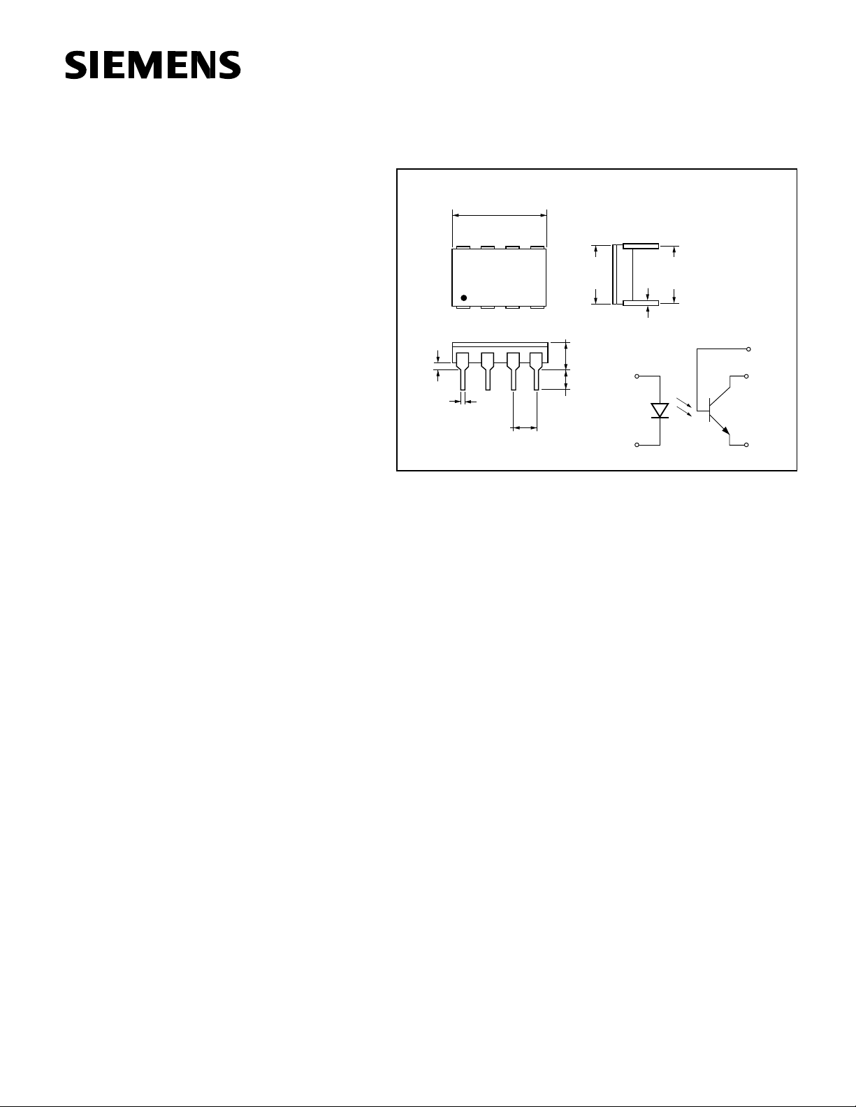
• Standard 8 Pin DIP Package
DESCRIPTION
The ILH100 is designed especially for hi-rel applications requiring optical isolation with high current
transfer ratio and low saturation VCE. Each optocoupler consists of a light emitting diode and a NPN
silicon phototransistor mounted and coupled in an 8
pin hermetically sealed DIP package. The ILH100's
low input current makes it well suited for direct
CMOS to LSTTL/TTL interfaces.
Dimensions in inches (mm)
.390±.005
(9.91±.13)
8 7 6 5
.300
(7.62)
typ.
7
Base
2
3
6
5
Collect
Emitter
.020
(.51)
min.
.018±.002
(.46±.05)
Siemens
XXX XXXX
XXYY
1 2 3 4
.100 ±.010
(2.54±.25)
.150
(3.81)
max.
.125
(3.18)
min.
.320
(8.13)
max.
Anode
Cathode
.010±.002
(.25±.05)
Maximum Ratings
Emitter
Reverse Voltage................................................................................6.0 V
Forward Current ..............................................................................60 mA
Peak Forward Current
(1)
...................................................................... 1 A
Power Dissipation.........................................................................150 mW
Derate Linearly from 25 °
C........................................................1.5 mW/ ° C
Detector
Collector–Emitter Voltage...................................................................70 V
Emitter–Base Voltage...........................................................................7 V
Collector–Base Voltage .....................................................................70 V
Continuous Collector Current..........................................................50 mA
Power Dissipation.........................................................................300 mW
Derate Linearly from 25 °
C........................................................3.0 mW/ ° C
Package
Input–Output Isolation Test V oltage
Storage Temperature Range ..........................................–65 °
(2)
..................................... 3000 VDC
C to +150 ° C
Operating Temperature Range..........................................–55 to +125 °
Junction Temperature......................................................................150 °
Soldering Time at 240 °
C, 1.6 mm from case................................ 10 sec.
Power Dissipation.........................................................................350 mW
Derate Linearly from 25 °
Notes:
1. Values applies for P
2. Measured between pins 1,2,3 and 4 shorted together and pins 5,6,7 and 8
shorted together. T
C........................................................3.5 mW/ ° C
1 ms, PRR£300 pps.
≤
W
=25 ° C and duration=1 second, RH=45%.
A
C
C
5–1

µ
Characteristics
Parameter
(T
=25 ° C, unless otherwise specified)
Α
Symbol Min. Typ. Max. Unit Condition
Emitter
Forward Voltage V
Reverse Breakdown Voltage V
Reverse Current I
Capacitance C
Thermal Resistance R
F
BR
R
J
TH
6VI
1.45 1.7 V I
0.01 10
µ AV
20 pF V
220
° C/W Junction to Lead
Detector
Collector-Emitter Saturation Voltage V
Base-Emitter Voltage V
Collector-Emitter Leakage Current I
CE(sat)
BE
CEO
0.25 0.4 V I
0.65 V I
550nAV
DC Forward Current Gain HFE 250 400 750 V
Saturated DC Forward Gain HFE
Capacitance C
Thermal Resistance R
CE
C
CB
C
EB
TH
(sat)
125 200 325 V
6.8
8.5
11
220
pF
pF
pF
° C/W Junction to Lead
Coupled Characteristics (-55 ° C to 100 ° C)
Saturated Current Transfer Ratio CTR
70 210 250 % I
(sat)
Current Transfer Ratio, Collector-Emitter
CTE
ce
100 300 450 % I
Current Transfer Ratio, Collector-Base
CTR
0.4 0.7 0.9 % I
cb
Isolation and Insulation
Common Mode Rejection Output High CM
Common Mode Rejection Output High CM
Package Capacitance C
Insulation Resistance R
Leakage Current, Input-Output I
IO
H
L
IO
IO
1000 2000 V/ µ sV
1000 2000 V/ µ sV
1.5 pF V
10
11
10
14
10
Ω
µ A Relative Humidity ≤ 50%,
=60 mA
F
=10 µ A
R
=6 V
R
=0 V, f=1 MHz
F
=20 µ A, I
B
=20 µ A
B
=10 V
CE
=10 V, I
CE
=0.4 V, I
CE
V
=5 V, f=1 MHz
CE
=10 mA V
F
=10 mA, V
F
=10 mA, V
F
=500 V
CM
I
=0 mA
F
=500 V
CM
I
=10 mA
F
=0 V, 1 MHz
IO
V
=500 VDC
IO
V
3000 VDC, 5 sec.
IO
CE
B
B
CE
CE
CB
p-p
p-p
=1 mA
=20 µ A
=20 µ A
=0.4 V
=10 V
=9.3 V
, V
CC
, V
CC
=5 V, R
=5 V, R
=1 K Ω ,
L
=1 K Ω ,
L
Typical Switching Speeds (T
Non-Saturated Switching
=25 ° C)
A
Symbol Typ. Max. Unit Test Condition
Delay td 0.8 2
Rise tr 2 5
Storage ts 0.4 1.5
Fall tf 2 5
Propagation-High to Low tpHL 1 3
Propagation-Low to High tpLH 1.5 4
Saturated Switching
(1)
Delay td 0.7 2
Rise tr 1 3
Storage ts 13.5 30
Fall tf 12 30
Propagation-High to Low tpHL 1.4 5
Propagation-Low to High tpLH 15 40
5–2
µ s
µ sV
µ sR
µ sI
µ s 50% of V
µ sR
µ sV
µ sV
µ sR
µ sI
µ sV
sR
=5 V
CC
=75 Ω
L
=10 mA
F
PP
=open
BE
=0.4 V
CE
=0.4 V
CE
=1 K Ω
L
=10 mA
F
=5 V,
CC
V
=1.5 V
TH
=open
BE
ILH100
A
A
C
A
C
A
A
A
C
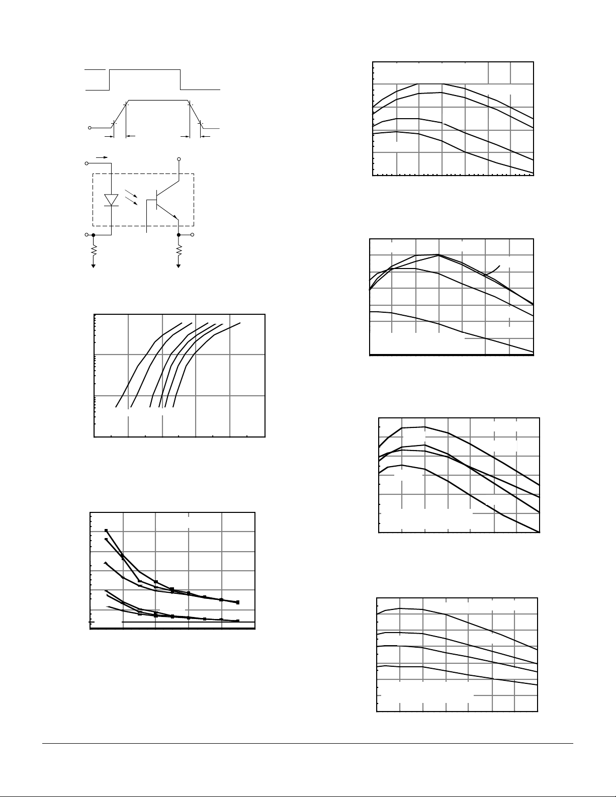
Figure 1. Switching time waveform and test schematic—
I
s
non-saturated test condition
nput
I
V
F
0
OUT
90%
t
r
I
F
100 Ω
Pulse Width=100 µ
Duty Cycle=1 %
10%
t
f
V
CC
V
OUT
R
L
Figure 2. Forward current versus forward voltage and
temperature
100
25°C
125°C
10
Figure 4. Normalized non-saturated current transfer ratio
versus temperature and LED current
1.2
Normalized to: Ta = 25 °
Vce = 10V, IF = 10 mA
1.0
10 m
0.8
1 mA
0.6
0.4
NCTRce - Normalized CTR
0.2
.5 mA
5 m
1251007550250-25-50
Ta - Ambient Temperature - °C
Figure 5. Normalized saturated current transfer ratio
versus temperature and LED current
1.1
1.0
Vce = 10 V
10 m
20 mA
0.9
0.8
0.7
0.6
Normalized to: Ta = 25°
0.5
Vce = 10V, IF = 10 mA
NCTRce - Normalized CTR
0.4
30 mA
60 mA
1251007550250-25-50
Ta - Ambient Temperature - °C
1
-55°C -25°C 0°C
.1
IF - Forward Current - mA
85°C
1.81.61.41.21.00.8
VF - Forward Voltage - V
Figure 3. Peak LED current versus duty factor refresh
rate and temperature
1.2
10KHz
Tj(max) = 150°C
1.0
1KHz
0.8
100 Hz
0.6
10KHz
0.4
1KHz
100Hz
0.2
60 mA
0.0
IF(Pk) - Peak LED Current - A
25°C
125°C
100806040200
DF - Duty Factor - %
Figure 6. Normalized saturated current transfer ratio
versus temperature and LED current
0.8
0.7
5 mA
Vce = 0.4 V
10 mA
0.6
0.5
0.4
Saturated CTR
0.3
NCTRce(sat) - Normalized
0.5 mA
1 mA
Normalized to Ta =25°C
Vce = 10 V, IF = 10 mA
0.2
1251007550250-25-50
Ta - Ambient Temperature - °C
Figure 7. Collector-emitter current versus temperature
and LED current
0.7
0.6
0.5
0.4
10 m
30 mA
Vce = 0.4 V
20 m
0.3
0.2
Saturated CTR
Normalized to: Ta = 25°
0.1
NCTR(sat)- Normalized
Vce = 10 V , IF = 10 mA
0.0
60 m
1251007550250-25-50
Ta - Ambient Temperature - °C
5–3
ILH100
 Loading...