

Siemens ILD755, IL755 Datasheet
.
.
.
.
)
)
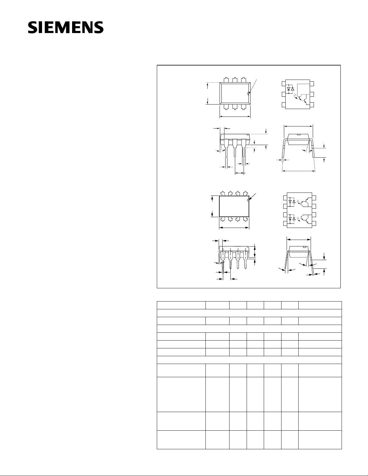
Dimensions in inches (mm)
Single Channel
Dual Channel
=5
FEATURES
• High Current Transfer Ratios, V
IL/ILD755-1: 750% at I
• IL/ILD755-2: 1000% at I
BV
>60 V
CEO
• AC or Polarity Insensitive Inputs
• Built-In Reverse Polarity Input Protection
• Industry Standard DIP Package
• Underwriters Lab File #E52744
• VDE #0884 Available with Option 1
DESCRIPTION
The IL/ILD755 are bidirectional input optically coupled isolators. They consist of two Gallium Arsenide infrared emitting diodes coupled to a silicon
NPN photodarlington per channel.
The IL755 are single channel Darlington optocouplers. The ILD755 has two isolated channels in a
single DIP package.
They are designed for applications requiring detection or monitoring of AC
Maximum Ratings
Emitter (Each Channel)
Continuous Forward Current.........................60 mA
Power Dissipation at 25 °
Derate Linearly from 25 °
Detector (Each Channel)
Collector-Emitter Breakdown Voltage...............60 V
Collector-Base Breakdown Voltage .................60 V
Power Dissipation at 25 °
IL755.......................................................200 mW
ILD755....................................................150 mW
Derate Linearly from 25 °
ILD755...................2.6 mW/ °
Package
Isolation Test V oltage (PK)
(t= 1 sec.)...................7500 VAC
Total Power Dissipation at 25 ° C Ambient
(LED Plus Detector)
IL755.......................................................250 mW
ILD755....................................................400 mW
Derate Linearly from 25 °
IL755...................................................3.3 mW/ °
ILD755................................................5.3 mW/ °
Creepage............................................... 7 mm min.
Clearance...............................................7 mm min.
Storage Temperature....................–55 °
Operating Temperature................–55 °
Lead Soldering Time at 260 °
BIDIRECTIONAL INPUT DARLINGTON OPTOCOUPLER
V
=2 mA
F
=1 mA
F
signals.
C..........................100 mW
C....................1.33 mW/ ° C
C
C
C
CE
CILD7552.0 mW/ ° C
/5300 VA C
PK
RMS
C to +150 ° C
C to +100 ° C
C....................10 sec.
.248 (6.30)
.256 (6.50)
.039
(1.00)
min.
4°
Typ.
.018 (0.45)
.022 (0.55)
255 (6.48)
268 (6.81)
4°
Typ.
018 (.46)
022 (.56)
Electrical Characteristics (T
Symbol Min. Typ. Max. Unit Condition
Emitter
Forward Voltage V
Detector
Package
C
C
DC Current
Transfer Ratio
IL755/ILD755-1
IL755/ILD755-2
Rise Time/Fall Time
IL/ILD755-1 50
Rise Time/Fall Time
IL/ILD755-2 70
5–1
F
BV
BV
I
CEO
V
CEsat
CTR
CEO
CBO
SINGLE CHANNEL
DUAL CHANNEL
Pin One ID.
12
3
4
5
6
.335 (8.50)
.343 (8.70)
.020 (.051) min.
.100 (2.54) Typ.
1
2
34
87
65
.379 (9.63)
.390 (9.91)
.030 (.76)
.045 (1.14)
.100 (2.54) Typ.
=25 ° C)
A
60 75 V I
60 90 V I
750
1000
Anode/
Cathode
Cathode/
Anode
.130 (3.30)
.150 (3.81)
.031 (0.80)
.035 (0.90)
Pin One I.D.
.130 (3.30)
.150 (3.81)
.030 (.76 )
.040 (1.02)
Anode/
Cathode
Cathode/
Anode
Anode/
Cathode
Cathode/
Anode
1.2 1.5 V I
10 100 nA V
1.0 I
NC
3°–9°
1
2
3
.300 (7.62)
18° Typ.
.010 (.25)
.014 (.35)
.300 (7.62)
.347 (8.82)
1
2
3
4
.305 Typ.
(7.75) Typ.
.008 (.20)
.012 (.30)
%
%
µ s
µ s
10°
Typ.
IL755
ILD755
6
Base
Collector
5
Emitter
4
Typ.
.110 (2.79)
.150 (3.81)
Emitter
8
Collector
7
Collector
6
5
Emitter
.115 (2.92
.135 (3.43
= ± 10 mA
F
=1 mA
C
=10 µ A
C
=10 V
CE
= ± 10 mA,
F
I
=10 mA
C
I
= ± 2 mA,
F
V
=5 V
CE
I
= ± 1 mA,
F
V
=5 V
CE
V
=10 V,
CC
R
=100 Ω ,
L
I
=2 mA
F
V
=10 V,
CC
R
=100 Ω ,
L
I
=1mA
F
V
C
V
C
V
A
0
C
V
V
g
C
V
V
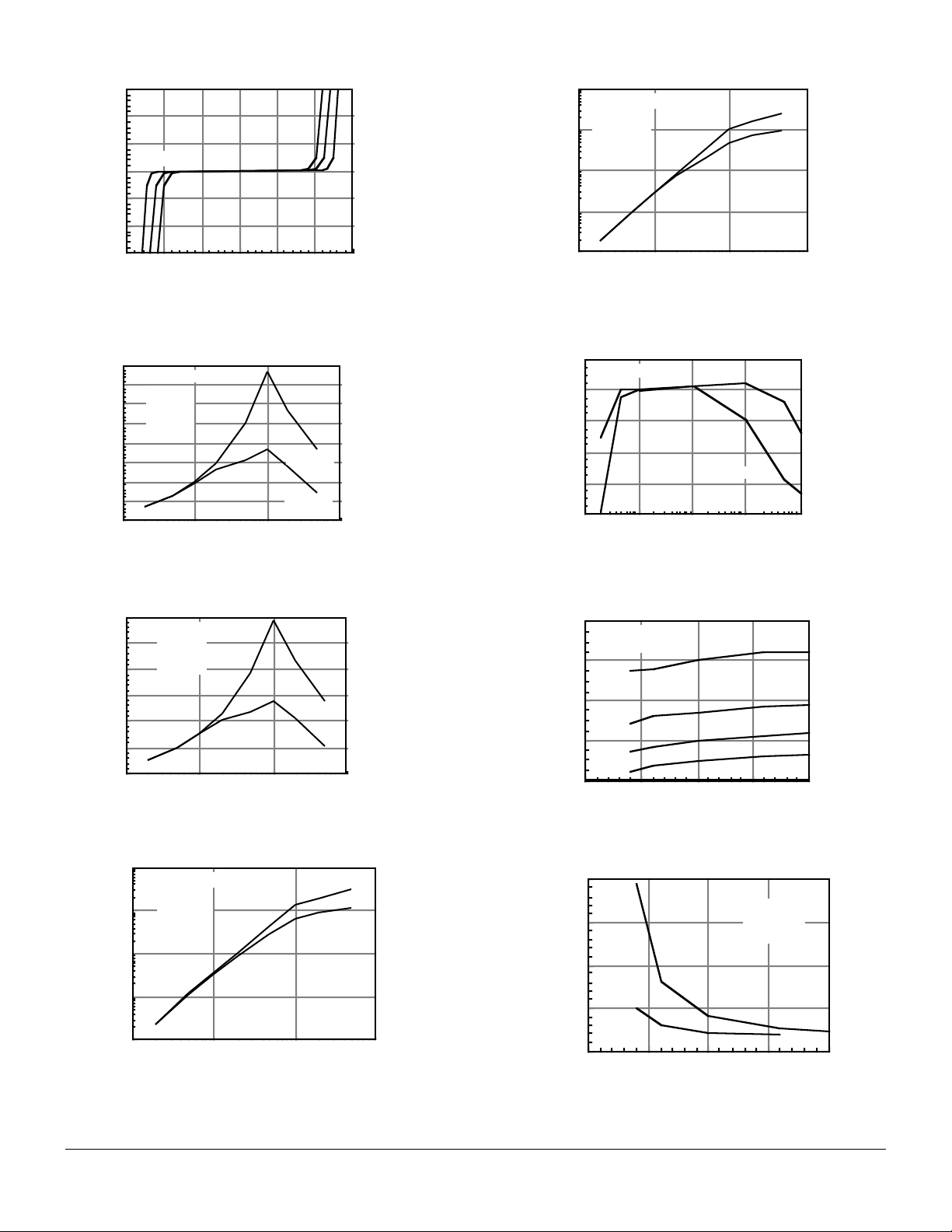
Figure 1. LED forward current versus forward voltage
60
40
20
25°C
0
-20
-40
-60
-1.5 -1.0 -0.5 0.0 0.5 1.0 1.5
IF - LED Forward Current - mA
VF - LED Forward Voltage - V
85°C
–55°C
Figure 2. Normalized non-saturated and saturated
CTRce versus LED current
4.0
Normalized to:
3.5
Ta = 25°
3.0
Vce = 5 V
IF = 1 mA
2.5
2.0
101.1
Vce = 5 V
Vce = 1
100
1.5
1.0
0.5
0.0
NCTRce - Normalized CTRce
IF - LED Current - mA
Figure 5. Normalized non-saturated and saturated
collector-emitter current versus LED current
10
Normalized to:
Ta = 25°C
IF = 10 mA
1
Vce = 5 V
.1
.01
NIce - Normalized Ice
.001
IF - LED Current - mA
Vce = 5
Vce = 1V
101.1
100
Figure 6. Non-saturated and saturated HFE versus
base current
10000
8000
6000
4000
2000
HFE - Forward Transfer Gain
Ta = 25°
0
.01 .1 1 10 100
Ib - Base Current - µA
Vce = 5
Vce = 1 V
Figure 3. Normalized non-saturated and saturated
CTRce versus LED current
3.0
Normalized to:
2.5
2.0
1.5
1.0
0.5
0.0
NCTRce - Normalized CTRce
Ta = 25°
Vce = 5
IF = 2 m
Vce = 5
Vce = 1 V
100101.1
IF - LED Current - mA
Figure 4. Normalized non-saturated and saturated
Ice versus LED current
10
Normalized to:
Ta = 25°
Vce = 5 V
10
IF = 2 mA
1
.1
NIce - Normalized Ice
.01
IF - LED Current - mA
Vce = 5 V
Vce = 1 V
100101.1
Figure 7. Low to high propagation delay versus
collector load resistance and LED current
80
Ta = 25°C, Vcc = 5
Vth = 1.5 V
60
40
Delay - µs
20
0
tpLH - Low/High Propagation
0 5 10 15 20
IF - LED Current - mA
1KΩ
220Ω
470Ω
100Ω
Figure 8. High to low propagation delay versus
collector load resistance and LED current
20
15
1KΩ
10
delay - µs
tpHL - High/Low Propagation
100Ω
5
0
0 5 10 15 20
IF - LED Current - mA
Ta = 25°C
Vcc = 5 V
Vth = 1.5
5–2
IL/ILD755
 Loading...