Siemens ILD621GB, ILD621, ILQ621GB, ILQ621 Datasheet

.
.
)
)
DUAL CHANNEL
QUAD CHANNEL
ILD621/621GB
ILQ621/621GB
MULTI-CHANNEL PHOTOTRANSISTOR
OPTOCOUPLER
FEATURES
• Alternate Source to TLP621-2/-4 and
TLP621GB-2/-4
• Current Transfer Ratio (CTR) at I
= 5 mA
F
ILD/Q621: 50% Min.
ILD/Q621GB: 100% Min.
• Saturated Current Transfer Ratio (CTR
at I
=1 mA
F
SAT
)
ILD/Q621: 60% Typ.
ILD/Q621GB: 30% Min.
• High Collector-Emitter Voltage, BV
CEO
=70 V
• Dual and Quad Packages Feature:
- Reduced Board Space
- Lower Pin and Parts Count
- Better Channel to Channel CTR Match
- Improved Common Mode Rejection
• Field-Effect Stable by TRIOS (TRansparent
IOn Shield)
• Isolation Test Voltage from Double Molded
Package, 5300 VAC
RMS
• Underwriters Lab File #E52744
• VDE 0884 Available with Option 1
Maximum Ratings (Each Channel)
Emitter
Reverse Voltage.................................................6 V
Forward Current ...........................................60 mA
Surge Current .................................................1.5 A
Power Dissipation.......................................100 mW
Derate from 25 °
C ................................1.33 mW/ ° C
Detector
Collector-Emitter Reverse Voltage ...................70 V
Collector Current.......................................... 50 mA
Collector Current (t <1 ms)..........................100 mA
Power Dissipation.......................................150 mW
Derate from 25 °
C ....................................–2 mW/ ° C
Package
Isolation Test V oltage
(t=1 sec.)......................................... 7500 VAC
(t=1 min.).......................................5300 VAC
RMS
Package Dissipation ILD620/GB............... 400 mW
Derate from 25 °
C ...............................5.33 mW/ ° C
Package Dissipation ILQ620/GB ..............500 mW
Derate from 25 °
Creepage............................................... 7 mm min.
Clearance...............................................7 min min.
Isolation Resistance
V
=500 V, T
IO
V
=500 V, T
IO
C ...............................6.67 mW/ ° C
=25 ° C ............................... ≥ 10
A
=100 ° C ............................. ≥ 10
A
12
11
Storage Temperature................... –55 ° C to +150 ° C
Operating Temperature................–55 °
C to +100 ° C
Junction Temperature....................................100 °
Soldering Temperature
(2 mm from case bottom)..........................260 °
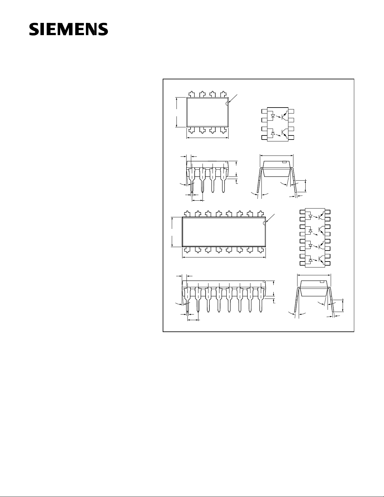
Dimensions in inches (mm)
Pin One I.D.
.100 (2.54)
Typ.
Typ.
12
87
.150 (3.81)
.130 (3.30)
.790 (20.07)
.779 (19.77 )
Cathode
Cathode
.040 (1.02)
.030 (.76 )
Anode
Anode
1
2
3
4
.305 typ.
(7.75) typ.
3°–9°
Pin One I.D.
.150 (3.81)
.130 (3.30)
10°
Typ.
.012 (.30)
.008 (.20)
Cathode
Cathode
Cathode
Cathode
.040 (1.02)
.030 (.76 )
8
7
6
5
Anode
Anode
Anode
Anode
Emitter
Collector
Collector
Emitter
.135 (3.43)
.115 (2.92)
1
2
3
4
5
6
7
8
.305 typ.
(7.75) typ.
10°
Typ.
3°–9°
.012 (.30)
.008 (.20)
.268 (6.81)
.255 (6.48)
4°
Typ.
.022 (.56)
.018 (.46)
268 (6.81)
255 (6.48)
4°
Typ.
.022 (.56)
.018 (.46)
34
65
.390 (9.91)
.379 (9.63)
.045 (1.14)
.030 (.76)
.045 (1.14)
.030 (.76)
.100 (2.54)
DESCRIPTION
The ILD/Q621 and ILD/Q621GB are multi-channel phototransistor optocou-
PK
plers that use GaAs IRLED emitters and high gain NPN silicon phototransistors. These devices are constructed using over/under leadframe optical
coupling and double molded insulation technology. This assembly process
offers a withstand test voltage of 7500 VDC.
The ILD/Q621GB is well suited for CMOS interfacing given the CTR
30% minimum at I
minimum CTR
of 1 mA. High gain linear operation is guaranteed by a
F
of 100% at 5 mA. The ILD/Q621 has a guaranteed CTR
CE
50% minimum at 5 mA. The TRansparent IOn Shield insures stable DC gain
in applications such as power supply feedback circuits, where constant DC
Ω
V
Ω
voltages are present.
IO
C
C
5–1
16
15
14
13
12
11
10
9
Emitter
Collector
Collector
Emitter
Emitter
Collector
Collector
Emitter
.135 (3.43
.115 (2.92
CEsat
CE
of
of

V
I
V
I
Characteristics
Symbol Min. Typ. Max. Unit Condition
Emitter
Forward Voltage V
Reverse Current I
Capacitance C
Thermal Resistance, Junction to Lead R
F
R
O
THJL
Detector
Capacitance C
Collector-Emitter Leakage Current I
Collector-Emitter Leakage Current I
Thermal Resistance, Junction to Lead R
CE
CEO
CEO
THJL
Package T ransfer Characteristics
Channel/Channel CTR Match CTRX/CTRY 1 to 1 3 to 1 I
ILD/Q621
Saturated Current Transfer Ratio CTR
Current Transfer Ratio CTR
Collector-Emitter Saturation Voltage V
CEsat
CE
CEsat
ILD/Q621GB
Saturated Current Transfer Ratio CTR
Current Transfer Ratio (Collector-Emit-
ter)
Collector-Emitter Saturation Voltage V
CTR
CEsat
CEsat
CE
Isolation and Insulation
Common Mode Rejection, Output High CMH 5000 V/ µ sV
Common Mode Rejection, Output Low CML 5000 V/ µ sV
Common Mode Coupling Capacitance C
CM
Package Capacitance CI-O 0.8 pF V
Insulation Resistance R
S
Channel to Channel Insulation 500 VAC
1 1.15 1.3 V I
0.01 10
µ AV
40 pF V
750
° C/W
6.8 pF V
10 100 nA V
250
500
µ
AT
° C/W
60 % I
50 80 600 % I
0.4 V I
30 % I
100 200 600 % I
0.4 V I
0.01 pF
12
10
Ω
F
R
F
CE
CE
A
F
F
F
F
F
F
F
CM
CM
mA
IO
V
IO
=10 mA
=6 V
=0 V, f=1 MHz
=5 V, f=1 MHz
=24 V
=85 ° C, V
=5 mA, V
=1 mA, V
=5 mA, V
=8 mA, I
=1 mA, V
=5 mA, V
=8 mA, I
=50 V
=50 V
CE
CE
CE
CE
=2.4 mA
CE
CE
CE
=0.2 mA
CE
, R
P-P
, R
P-P
=0 V, f=1 MHz
=500 V, T
A
=24 V
=5 V
=0.4 V
=5 V
=0.4 V
=5 V
=1 k Ω , I
L
=1 k Ω , I
L
=25 ° C
=0 mA
F
=10
F
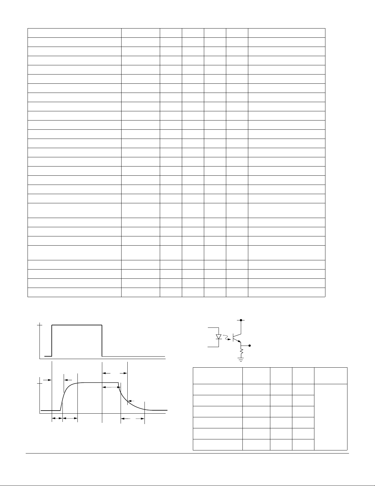
Switching Times
Figure 1. Non-saturated switching timing
F
t
t
0
PLH
t
D
t
R
PHL
t
S
50%
t
F
Figure 2. Non-saturated switching timing
VCC=5
=10 mA
F
V
F=10 KHz,
DF=50 %
Characteristic Symbol Typ. Unit Test
On Time T
Rise Time t
Off Time t
Fall Time t
Propagation H-L t
Propagation L-H t
5–2
O
RL=75 Ω
ON
R
OFF
F
PHL
PLH
3.0
20
2.3
2.0
1.1
2.5
µ sI
µ s
µ s
µ s
µ s
µ s
Condition
=
±
10 mA
F
V
=5 V
CC
R
=75 Ω
L
50% of V
ILD/Q621/GB
PP
 Loading...