

Siemens ILD610 Datasheet
.
.
)
)
r
r
ILD610 SERIES
DUAL PHOTOTRANSISTOR
OPTOCOUPLER
FEATURES
• Dual Version of SFH610 Series
• High Current Transfer Ratios
ILD610-1, 40-80%
ILD610-2, 63-125%
ILD610-3, 100-200%
ILD610-4, 160-320%
• Isolation T est V oltage, 5300 V
•V
•V
0.25 ( ≤ 0.4) V at I
CEsat
=70 V
CEO
RMS
=10 mA, I
F
=2.5 mA
C
• Underwriters Lab File #E52744
V
• VDE #0884 Available with Option 11
DE
DESCRIPTION
The ILD610 Series is a dual channel optocoupler
series for high density applications. Each channel
consists of an optically coupled pair with a Gallium
Arsenide infrared LED and a silicon NPN phototransistor. Signal information, including a DC
level, can be transmitted by the device while maintaining a high degree of electrical isolation between
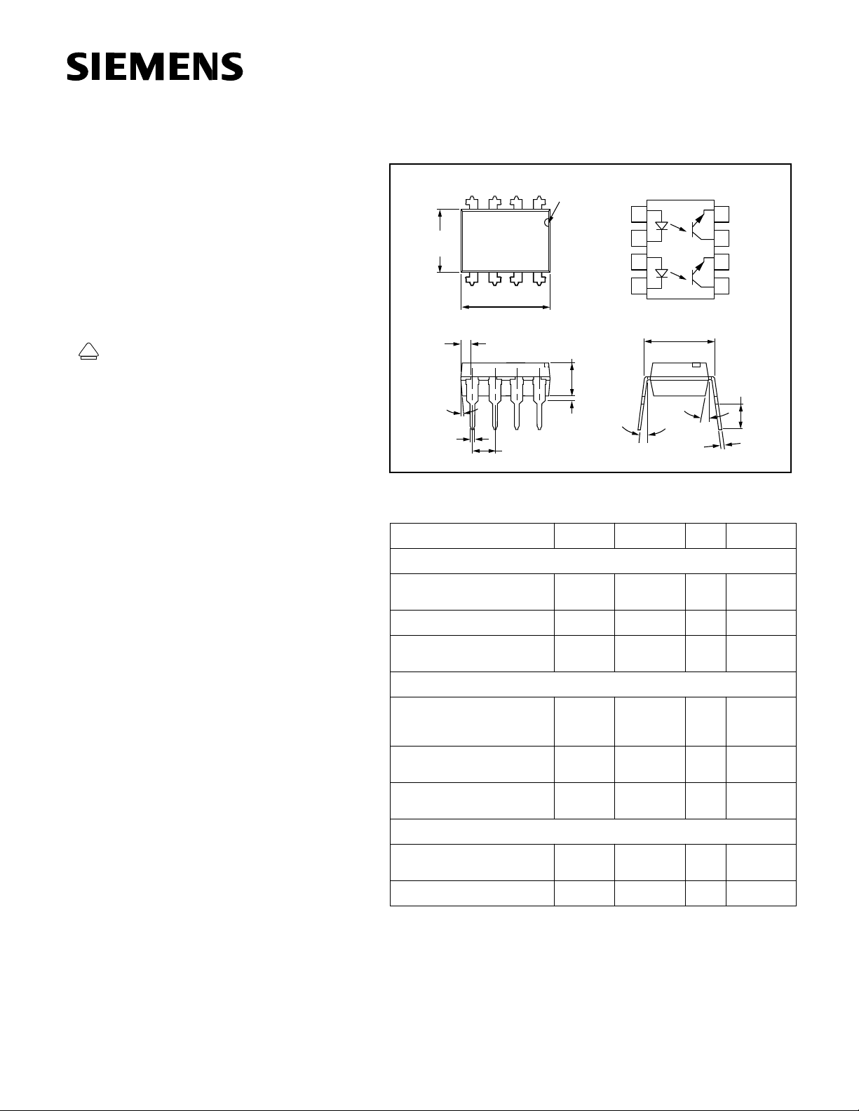
Dimensions in inches (mm)
34
268 (6.81)
255 (6.48)
65
.390 (9.91)
.379 (9.63)
.045 (1.14)
.030 (.76)
4° Typ.
.022 (.56)
.018 (.46)
.100 (2.54) Typ.
Pin One I.D.
12
87
.150 (3.81)
.130 (3.30)
.040 (1.02)
.030 (.76 )
Anode
Cathode
Anode
Cathode
1
2
3
4
.305 Typ.
(7.75) Typ.
10° Typ.
3°–9°
.012 (.30)
.008 (.20)
8
Emitter
7
Collecto
6
Emitter
5
Collecto
.135 (3.43
.115 (2.92
input and output. The ILD610 Series is the dual version of SFH610 Series and uses a repetitive pin-out
Electrical Characteristics (T
configuration instead of the more common alternating pin-out used in most dual couplers.
Maximum Ratings (Each Channel)
Emitter
Emitter
Forward Voltage V
Reverse Voltage.................................................6 V
Surge Forward Current (t £10 ms)...................1.5 A
Reverse Current I
Total Power Dissipation..............................100 mW
Derate Linearly from 25 °
C......................1.3 mW/ ° C
Capacitance C
DC Forward Current......................................60 mA
Detector
Collector-Emitter Voltage..................................70 V
Collector Current ..........................................50 mA
Collector Current (t ≤
1 ms)..........................100 mA
Total Power Dissipation..............................150 mW
Derate Linearly from 25 °
C......................2.0 mW/ ° C
Package
Isolation Test V oltage (t=1 sec.)........5300 VAC
Isolation Resistance
V
=500 V, T
IO
V
=500 V, T
IO
=25 ° C ............................... ≥ 10
A
=100 ° C ............................. ≥ 10
A
RMS
12
11
Ω
Ω
Storage Temperature ...................–55 ° C to +150 ° C
Operating Temperature ...............–55 °
Junction Temperature ...................................100 °
Lead Soldering Time at 260 °
C....................10 sec.
C to +100 ° C
C
Detector
Breakdown Voltage
Collector-Emitter
Emitter-Collector
Collector-Emitter Dark
Current
Capacitance C
Package
Collector-Emitter Saturation
Voltage
Coupling Capacitance C
=25 ° C)
A
Symbol Typ. Unit Condition
R
BV
BV
I
CEO
V
F
O
CEO
CEO
CE
CEsat
C
1.25
( ≤ 1.65)
0.01 (
25 pF V
90 ( ≥ 70)
7.0 ( ≥ 6.0)VV
2 ( ≤ 50) nA V
7pFV
0.25
( ≤ 0.40)
0.35 pF
VI
≤
10) µ AV
VI
=60mA
F
R
R
f=1 MHz
I
C
I
=10 µ A
E
CE
CE
f=1 MHz
=10 mA,
F
I
C
=6V
=0 V,
=10 µ A
=10 V
=5 V,
=2.5 mA
5–1
1,
CTR
I
CTR
I
CEO
=10 mA, V
F
1,
I
=1 mA, V
F
(V
=10 V) 2 ( ≤ 50) 2 ( ≤ 50) 5 ( ≤ 100) 5 ( ≤ 100) nA
CE
=5 V 40-80 63-125 100-200 160-320 %
CE
=5 V 13 min. 22 min. 34 min. 56 min. %
CE
CTR will match within a ratio of 1.7:1
-1 -2 -3 -4
Switching Characteristics
Linear Operation (without saturation)
I
=10 mA, V
F
CC
=5 V, R
-1 -2 -3 -4
Turn on time t
Rise time t
Turn off time t
Fall time t
Switching Operation
(with saturation)
on
r
off
f
3.0 3.2 3.6 4.1
2.0 2.5 2.9 3.3
2.3 2.9 3.4 3.7
2.0 2.6 3.1 3.5
V
CC
=5 V, R
=1 Ω , T ypical
C
-1
I
= 20 mA-2I
F
Turn on time t
Rise time t
Turn off time t
Fall time t
on
r
off
f
3.0 4.3 4.6 6.0
2.0 2.8 3.3 4.6
18 2.9 3.4 25
11 2.6 3.1 15
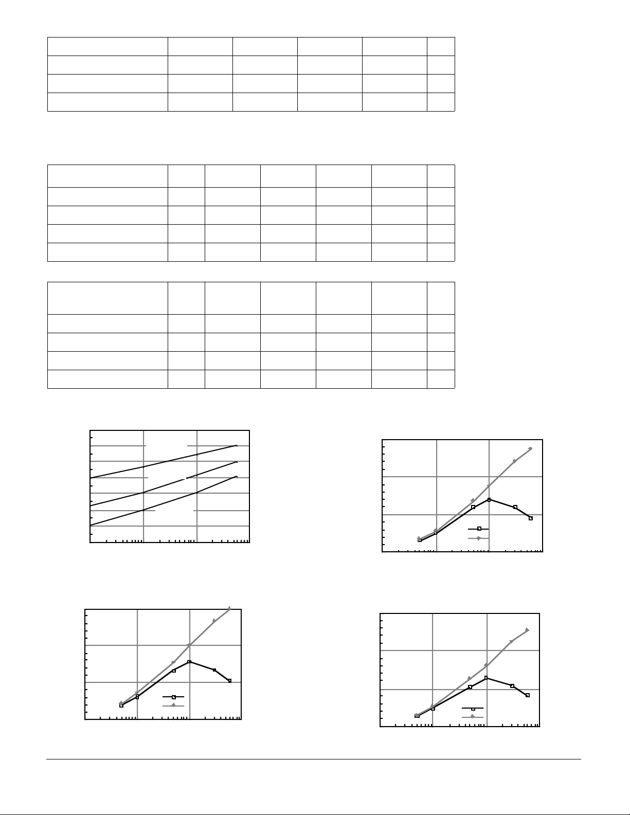
Figure 1. Forward voltage versus forward current
1.4
1.3
Ta = -55°C
1.2
1.1
Ta = 25°C
1.0
0.9
Ta = 85°C
0.8
VF - Forward Voltage - V
0.7
100101.1
IF - Forward Current - mA
Figure 2. Normalized non-saturated and saturated
CTR at T
=25 ° C versus LED current
A
1.5
Normalized to:
Vce = 5V, IF = 10mA
Ta = 25°C
1.0
CTRce(sat) Vce = 0.4V
=75 Ω , T ypical
C
= 10 mA-3I
F
l
= 10 mA-4I
F
µ s
µ s
µ s
µ s
= 5 mA
F
µ s
µ s
µ s
µ s
Figure 3. Normalized non-saturated and saturated
CTR at T
=50 ° C versus LED current
A
1.5
Normalized to:
Vce = 5V, IF = 10mA, Ta = 25°C
CTRce(sat) Vce = 0.4V
1.0
Ta = 50°C
0.5
NCTR - Normalized CTR
0.0
IF - LED Current - mA
NCTR(SAT)
NCTR
100101.1
Figure 4. Normalized non-saturated and saturated
CTR at T
=70 ° C versus LED curent
A
1.5
Normalized to:
Vce = 5V, IF = 10mA
Ta = 25°C
1.0
CTRce(sat) Vce = 0.4V
0.5
NCTR - Normalized CTR
0.0
IF - LED Current - mA
NCTR(SAT)
NCTR
0.5
Ta = 70°C
NCTR(SAT)
NCTR - Normalized CTR
100101.1
0.0
NCTR
100101.1
IF - LED Current - mA
5–2
ILD610
 Loading...