

Siemens IL255 Datasheet
)
)
.
.
F
EATURES
• AC or Polarity Insensitive Inputs
• Continuous Forward Current, 130 mA
• Applications—Telecommunications
– Ring Detection
– Loop Current Detector
• Built-in Reverse Polarity Input Protection
• Improved CTR Symmetry
• Industry Standard DIP Package
• Underwriters Lab File #E52744
V
• VDE Approval #0884 Applied For
DE
DESCRIPTION
The IL255 is a bidirectional input optically coupled isolator consisting of two high current Gallium Arsenide infrared LEDs coupled to a
silicon NPN phototransistor. The IL255 has a
minimum CTR of 20%
This optocoupler is ideal for applications requiring AC signal detection and monitoring.
Maximum Ratings
Emitter
Peak Pulsed Current (1 µ s, 300 pps) ...........3 A
Continuous Forward Current......... 130 mA RMS
Power Dissipation at 25 °
Derate Linearly from 25 °
C....................175 mW
C................ 2.3 mW/ ° C
Detector
Collector-Emitter Breakdown Voltage ........30 V
Emitter-Base Breakdown Voltage ................ 5 V
Collector-Base Breakdown Voltage............70 V
Power Dissipation at 25 °
Derate Linearly from 25 °
C....................200 mW
C................ 2.6 mW/ ° C
Package
Isolation Test Voltage................... 5300 VAC
RMS
Between Emitter and Detector
Refer to Standard Climate
23 °
C/50%RH, DIN 50014
Creepage...........................................min. 7 mm
Clearance..........................................min. 7 mm
Isolation Resistance
V
=500 V, T
IO
V
=500 V, T
IO
=25 ° C........................... ≥ 10
A
=100 ° C......................... ≥ 10
A
12
11
Ω
Ω
Total Dissipation at 25 ° C....................... 250 mW
Derate Linearly from 25 °
Storage Temperature ............. –55 °
Operating Temperature .........–55 °
Lead Soldering Time at 260 °
C................ 3.3 mW/ ° C
C to +150 ° C
C to +100 ° C
C ...............10 sec.
SINGLE CHANNEL
IL255
BIDIRECTIONAL INPUT
OPTOCOUPLER
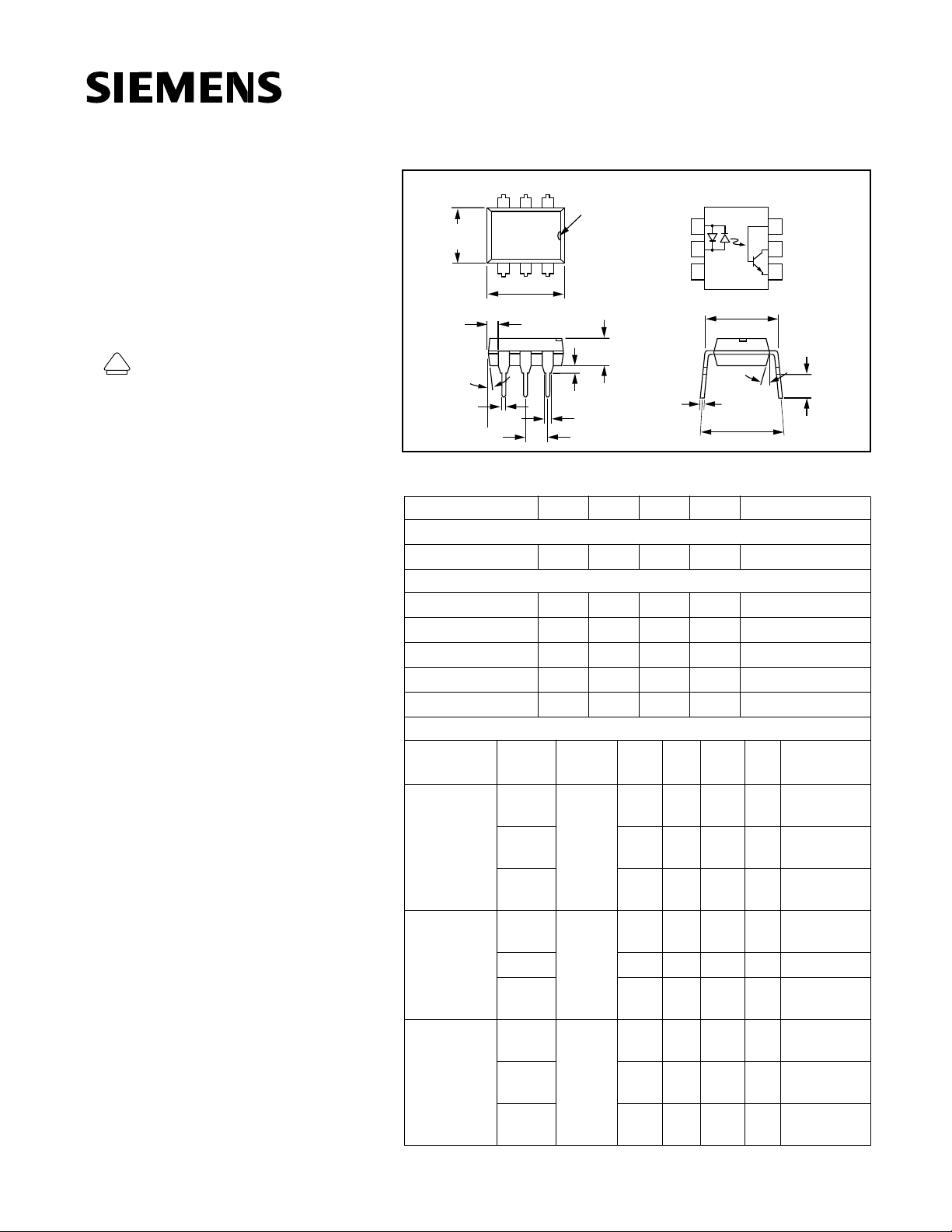
Package Dimensions in Inches (mm)
12
3
.248 (6.30)
.256 (6.50)
4
5
.335 (8.50)
4°
typ.
.343 (8.70)
.039
(1.00)
min.
018 (0.45)
022 (0.55)
Electrical Characteristics (T
Parameter Min. Typ. Max. Unit Test Condition
Emitter
Forward Voltage 1.4 1.7 V I
Detector
BV
CEO
BV
ECO
BV
CBO
BV
EBO
I
CEO
Package
Parameter Device Symbol Min. Typ. Max. Unit
IL255
Current
Transfer
IL255-1 20 80 %
Ratio
IL255-2 50 %
Current
Transfer
Ratio
Symmetry
IL255 0.33 3.0
IL255-1
IL255-2 0.5 1.0 2.0
IL255
Collectoremitter
Saturation
IL255-1 0.1 0.2 V
Voltage
IL255-2 0.4 V
Pin One ID.
6
.130 (3.30)
.150 (3.81)
.020 (.051) min.
.031 (0.80)
.035 (0.90)
.100 (2.54) Typ.
=25 ° C)
A
30 50 V I
710 VI
70 V I
7VI
550nAV
CTR
V
CE
(sat)
Anode/
Anode
NC
1
2
3
.300 (7.62)
18° typ.
.300 (7.62)
.347 (8.82)
typ.
.010 (.25)
.014 (.35)
Cathode
Cathode/
20 %
0.4 V
6
Base
Collector
5
Emitter
4
.110 (2.79
.150 (3.81
= ± 100 mA
F
=10 mA
C
=10 µ A
E
=100 µ A
C
=100 µ A
E
=10 V
CE
Test
Condition
I
= ± 10 mA,
F
V
CE
= ± 100 mA,
I
F
V
CE
= ± 10 mA,
I
F
V
CE
I
= ± 10 mA,
F
V
CE
= ± 10 mA,
I
F
V
CE
= ± 10 mA,
I
F
I
=0.5 mA
C
= ± 100 mA,
I
F
I
=1 mA
C
= ± 16 mA,
I
F
I
=2 mA
C
=10 V
=2 V
=10 V
=10 V
=10 V
JUNE 1995
Figure 1. LED forward current versus
forward voltage
Figure 2. Maximum LED current
versus ambient temperature
Figure 3. Maximum LED power
dissipation
Figure 4. Current transfer ratio versus
LED current and collector-emitter
voltage
Figure 5. Saturated and non-saturated
collector-emitter current versus LED
current
Figure 6. Saturated and non-saturated
collector-emitter current versus LED
current
Figure 7. Collector-emitter current versus LED
collector-emitter voltage
12
10
8
6
4
2
0
Ice–Collector Emitter Current – mA
0 0.2 0.4 0.6 1.0 1.4 1.8 2.2
Vce–Collector Emitter Voltage – V
=8 mA
I
F
I
F
I
F
=7 mA
=6 mA
I
=5 mA
F
=4 mA
I
F
=3 mA
I
F
IF=2 mA
I
=1 mA
F
IL255
2
 Loading...