Siemens BTS933 Datasheet

)
)
HITFETBTS 933
Smart Lowside Power Switch
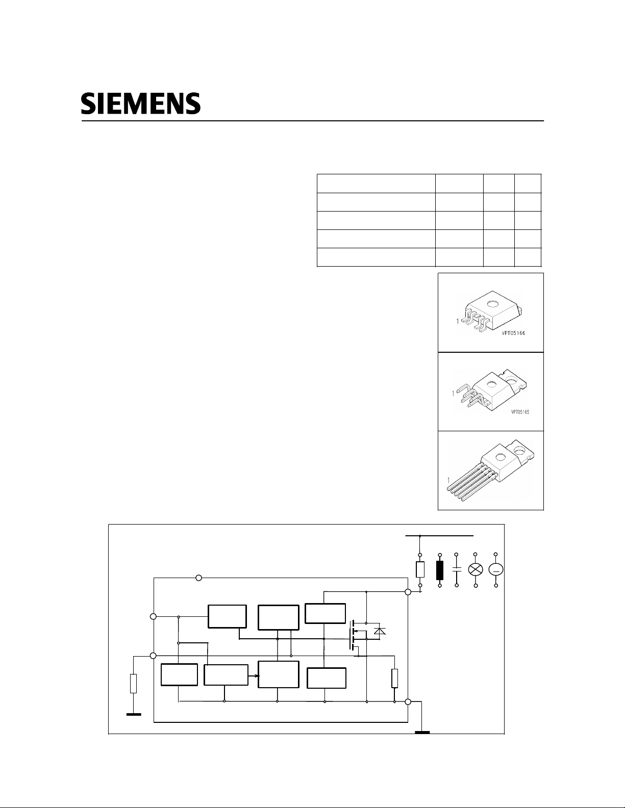
Features
• Logic Level Input
• Input Protection (ESD)
Product Summary
Drain source voltage
On-state resistance
• Thermal Shutdown
• Overload protection
• Short circuit protection
Nominal load current A
Clamping energy mJ
• Overvoltage protection
• Current limitation
• Maximum current adjustable with external resistor
• Current sense
• Status feedback with external input resistor
• Analog driving possible
Application
• All kinds of resistive, inductive and capacitive loads in switching or
linear applications
• µC compatible power switch for 12 V and 24 V DC applications
• Replaces electromechanical relays and discrete circuits
General Description
V
DS
R
DS(on
I
D(lim)
I
D(ISO
E
AS
50
3
7
2000
V60
mΩ
ACurrent limit
N channel vertical power FET in Smart SIPMOS chip on chip technology. Fully protected by embedded protected functions.
V
Drain
Source
HITFET
LOAD
3
5
1
IN
CC
4
R
CC
ESD
Semiconductor Group
2
NC
dv/dt
limitation limitation
Overload
protection
Current
Over-
temperature
protection
Overvoltage
protection
Short circuit
Short circuit
protection
protection
Page 1
bb
+
M
14.07.1998

Maximum Ratings at Tj = 25 °C unless otherwise specified
j
BTS 933
Parameter
Drain source voltage
Drain source voltage for short circuit protection
R
= 0 Ω
CC
R
V
CC
≤ 10V
IN
V
IN
1)
> 10V
without
Continuous input current
-0.2V ≤
V
< -0.2V or
IN
Operating temperature
Storage temperature
Power dissipation
T
= 25 °C
C
Unclamped single pulse inductive energy
I
D(ISO)
= 7 A
Electrostatic discharge voltage (Human Body Model)
according to MIL STD 883D, method 3015.7 and
EOS/ESD assn. standard S5.1 - 1993
Symbol UnitValue
V
DS
V
DS(SC)
60 V
15
50
I
IN
no limit
I
| ≤ 2
|
IN
T
T
P
E
V
stg
tot
AS
ESD
- 55 ... +150
90 W
2000 mJ
3000 V
mA
°C- 40 ... +150
Load dump protection
V
=low or high;
IN
= 400 ms,
t
d
= 400 ms,
t
d
R
= 2 Ω,
I
R
= 2 Ω,
I
V
=13.5 V
A
V
LoadDump
I
=0,5*7A
D
I
= 7A
D
2)
=
V
+
V
A
S
V
LD
90
74
DIN humidity category, DIN 40 040 E
IEC climatic category; DIN IEC 68-1 40/150/56
Thermal resistance
junction - case:
junction - ambient:
SMD version, device on PCB:
1
A sensor holding current of 500 µA has to be guaranted in the case of thermal shutdown (see also page 3)
2
V
Loaddump
3
Device on 50mm*50mm*1.5mm epoxy PCB FR4 with 6cm2 (one layer, 70 µm thick) copper area for Drain connection. PCB is vertical
without blown air.
is setup without the DUT connected to the generator per ISO 7637-1 and DIN 40839
Semiconductor Group
3)
Page 2
R
R
R
thJC
thJA
thJA
1.4 K/W
75
45
14.07.1998

Electrical Characteristics
BTS 933
Parameter
Characteristics
T
= - 40 ...+ 150°C,
j
V
= 32 V,
DS
I
= 1,4 mA
D
T
j
Input current - normal operation,
V
= 10 V
IN
Input current - current limitation mode,
V
= 10 V
IN
Input current - after thermal shutdown,
V
= 10 V
IN
I
= 10 mA
D
= -40...+150 °C,
V
= 0 V
IN
I
<
D
I
D(lim)
I
I
:
=
I
D
=0 A:
D
D(lim)
Input holding current after thermal shutdown
T
= 25 °C
j
T
= 150 °C
j
Symbol UnitValues
60
-Off state drain current
1.3Input threshold voltage
-
60
1000
:
V
DS(AZ)
I
DSS
V
IN(th)
I
IN(1)
I
IN(2)
I
IN(3)
I
IN(H)
500
300
max.typ.min.at Tj=25°C, unless otherwise specified
-Drain source clamp voltage
-
73 V
10 µA
1.7 2.2
30 55 µA
150
2500
-
-
350
4000
-
-
V
On-state resistance
I
= 7 A,
D
I
= 7 A,
D
V
IN
V
IN
= 5 V,
= 5 V,
T
T
On-state resistance
I
= 7 A,
D
I
= 7 A,
D
V
IN
V
V
= 10 V,
= 10 V,
IN
= 10 ,
IN
V
DS
T
= 0.5 V,
Semiconductor Group
= 25 °C
j
= 150 °C
j
T
= 25 °C
j
= 150
j
T
= 85 °C
C
Page 3
R
DS(on)
R
DS(on)
I
D(ISO)
-
-
-
-
7Nominal load current (ISO 10483)
50
90
40
75
-
60
120
50
100
- A
mΩ
mΩ
14.07.1998

Electrical Characteristics
j
BTS 933
Parameter
Symbol Values Unit
at Tj=25°C, unless otherwise specified min. typ. max.
Characteristics
Initial peak short circuit current limit
V
= 10 V,
IN
V
DS
= 12 V
Current limit 1)
V
= 10 V,
IN
T
= -40...+150 °C, without
j
V
= 10 V,
IN
T
= -40...+150 °C,
j
V
DS
V
DS
= 12 V,
= 12 V,
R
CC
t
= 350 µs,
m
R
CC
t
= 350 µs,
m
= 0 Ω
I
D(SCp)
I
D(lim)
- 125 - A
3
60
7
80
12
100
Dynamic Characteristics
Turn-on time
R
= - Ω,
L
V
IN
Turn-off time
R
= - Ω,
L
V
IN
V
to 90%
IN
= 0 to 10 V,
V
to 10%
IN
= 10 to 0 V,
V
V
Slew rate on 70 to 50%
R
= - Ω,
L
V
= 0 to 10 V,
IN
V
Slew rate off 50 to 70%
R
= - Ω,
L
V
= 10 to 0 V,
IN
V
I
D
= 12 V
bb
I
D
= 12 V
bb
V
bb
= 12 V
bb
V
bb
= 12 V
bb
:
:
:
:
t
on
t
off
-dVDS/dt
/dt
DS
off
-
on
-
40 100-
70 170
31-
1 3dV
µs
V/µs
Protection Functions
°CThermal overload trip temperature 165 -150
mJ
-
-
Unclamped single pulse inductive energy
I
= 7 A,
D
I
= 7 A,
D
T
= 25 °C,
j
T
= 150 °C,
j
V
bb
V
= 32 V
= 32 V
bb
T
t
E
AS
2000
450
-
-
Inverse Diode
Inverse diode forward voltage
I
= 5*7A,
F
1
Device switched on into existing short circuit (see diagram Determination of I
might be exceeded for max. 50 µs in case of short circuit occurs while the device is on condition
Semiconductor Group
t
= 300 µs,
m
V
= 0 V
IN
Page 4
V
SD
. Dependant on the application, these values
D(lim)
1.08 -- V
14.07.1998
 Loading...