

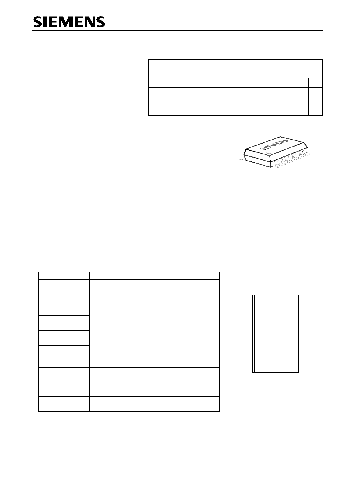
Smart Four Channel Highside Power Switch
O
O
:
l
O
R
ON
Nominal load current
I
L(NOM)
2.9
4.3
6.3
Current limitation
I
101010
Product Summary
Features
•
Overload protection
•
Current limitation
•
Short-circuit protection
•
Thermal shutdown
•
Overvoltage protection
(including load dump)
•
Reverse battery protection
•
Undervoltage and overvoltage shutdown
with auto-restart and hysteresis
•
Open drain diagnostic output
•
Open load detection in ON-state
•
CMOS compatible input
•
Loss of ground and loss of V
•
Electrostatic discharge (ESD) protection
1
)
protection
bb
Application
•
µC compatible power switch with diagnostic feedback
for 12 V DC grounded loads
•
Most suitable for resistive and lamp loads
•
Replaces electromechanical relays and discrete circuits
vervoltage Protection
perating voltage
active channels
n-state resistance
L(SCr)
PROFET® BTS720L1
V
bb(AZ)
V
bb(on)
one
two parallelfour paralle
5.0 ... 24 V
100 50 25
43 V
m
Ω
A
A
General Description
N channel vertical power FET with charge pump, ground referenced CMOS compatible input and diagnostic
feedback, monolithically integrated in Smart SIPMOS technology. Fully protected by embedded protection
functions.
Pin Definitions and Functions
Pin Symbol Function
1,10,
11,12,
15,16,
19,20
3 IN1 Input 1 .. 4, activates channel 1 .. 4 in case of
5 IN2 logic high signal
7 IN3
9 IN4
18 OUT1 Output 1 .. 4, protected high-side power output
17 OUT2 of channel 1 .. 4. Design the wiring for the
14 OUT3 max. short circuit current
13 OUT4
4 ST1/2 Diagnostic feedback 1/2 of channel 1 and
8 ST3/4 Diagnostic feedback 3/4 of channel 3 and
2 GND1/2 Ground 1/2 of chip 1 (channel 1 and channel 2)
6 GND3/4 Ground 3/4 of chip 2 (channel 3 and channel 4)
V
bb
Positive power supply voltage. Design the
wiring for the simultaneous max. short circuit
currents from channel 1 to 4 and also for low
thermal resistance
channel 2, open drain, low on failure
channel 4, open drain, low on failure
Pin configuration
Vbb1
GND1/2 2 19 V
IN1 3 18 OUT1
ST1/2 4 17 OUT2
IN2 5 16 V
GND3/4 6 15 V
IN3 7 14 OUT3
ST3/4 8 13 OUT4
IN4 9 12 V
Vbb10 11 V
•
(top view)
20 V
bb
bb
bb
bb
bb
bb
)
1
With external current limit (e.g. resistor R
connection, reverse load current limited by connected load.
Semiconductor Group Page 1 of 14 26.Feb.96
=150 Ω) in GND connection, resistor in series with ST
GND
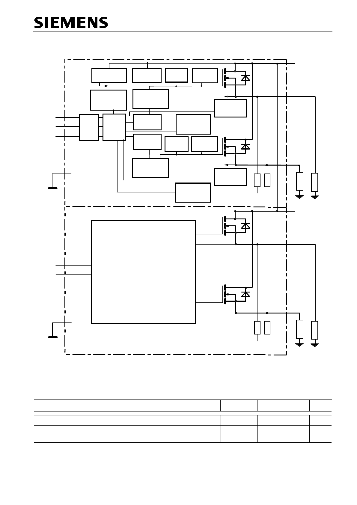
Block diagram
Four Channels; Open Load detection in on state;
Voltage
source
V
Logic
Voltage
sensor
3
IN1
IN2
5
4
ESD
ST1/2
Logic
Overvoltage
protection
Level shifter
Rectifier 1
Charge
pump 1
Charge
pump 2
Current
limit 1
Current
limit 2
Gate 1
protection
Open load
Short to Vbb
detection 1
Gate 2
protection
Temperature
sensor 1
+ V
Channel 1
OUT1
Channel 2
BTS720L1
bb
Leadframe
18
Signal GND
Chip 1
Signal GND
Chip 2
2
7
9
8
6
GND1/2
IN3
IN4
ST3/4
GND3/4
Chip 1
PROFET
Chip 2
Level shifter
Rectifier 2
Open load
Short to Vbb
detection 2
Logic and protection circuit of chip 2
(equivalent to chip 1)
Temperature
sensor 2
OUT2
RR
O1
RR
O3
GND1/2
+ V
Channel 3
OUT3
Channel 4
OUT4
GND3/4
O2
bb
O4
17
Load
Load GND
Leadframe
14
13
Load
Load GND
Leadframe connected to pin 1, 10, 11, 12, 15, 16, 19, 20
Maximum Ratings
at
= 25°C unless otherwise specified
j
T
Parameter Symbol Values Unit
Supply voltage (overvoltage protection see page 4)
Supply voltage for full short circuit protection
T
= -40 ...+150°C
j,start
V
V
bb
bb
43 V
24 V
Semiconductor Group Page 2 26.Feb.96
BTS720L1
Maximum Ratings at
T
= 25°C unless otherwise specified
j
Parameter Symbol Values Unit
Load current (Short-circuit current, see page 5)
)
Load dump protection
)
3
R
= 2 Ω,
I
t
= 200 ms; IN = low or high,
d
each channel loaded with
2
V
LoadDump
R
= 4.7 Ω,
L
=
U
+
V
,
A
U
s
Operating temperature range
Storage temperature range
Power dissipation (DC)
(all channels active)
5
T
T
Electrostatic discharge capability (ESD)
= 13.5 V
A
= 25°C:
a
= 85°C:
a
I
L
V
Load dump
T
j
T
stg
P
tot
V
ESD
self-limited A
)
4
-40 ...+150
60 V
°C
-55 ...+150
3.7
W
1.9
1.0 kV
(Human Body Model)
Input voltage (DC)
Current through input pin (DC)
Current through status pin (DC)
see internal circuit diagram page 8
V
I
I
IN
ST
IN
-10 ... +16 V
±2.0
mA
±5.0
Thermal resistance
junction - soldering point
junction - ambient
5)
5),6)
each channel:
one channel active:
all channels active:
R
R
thjs
thja
15 K/W
41
34
Electrical Characteristics
Parameter and Conditions,
at Tj = 25 °C,
V
= 12 V unless otherwise specified
bb
each of the four channels
Load Switching Capabilities and Characteristics
On-state resistance (Vbb to OUT)
IL = 2 A each channel,
two parallel channels,
four parallel channels,
)
2
Supply voltages higher than V
150 Ω resistor in the GND connection and a 15 kΩ resistor in series with the status pin. A resistor for input
protection is integrated.
3)
R
= internal resistance of the load dump test pulse generator
I
4)
V
Load dump
)
5
Device on 50mm*50mm*1.5mm epoxy PCB FR4 with 6cm
connection. PCB is vertical without blown air. See page 14
)
6
Soldering point: upper side of solder edge of device pin 15. See page 14
is setup without the DUT connected to the generator per ISO 7637-1 and DIN 40839
require an external current limit for the GND and status pins, e.g. with a
bb(AZ)
T
= 25°C:
j
T
= 150°C:
j
T
= 25°C:
j
T
= 25°C:
j
Symbol Values Unit
min typ max
R
ON
--
85
170
100
200
43
22
2
(one layer, 70µm thick) copper area for V
mΩ
50
25
bb
Semiconductor Group Page 3 26.Feb.96

BTS720L1
Parameter and Conditions,
at Tj = 25 °C,
V
= 12 V unless otherwise specified
bb
each of the four channels
Nominal load current one channel active:
two parallel channels active:
four parallel channels active:
Device on PCB5),
T
= 85°C,
a
T
≤ 150°C
j
Output current while GND disconnected or pulled
up; V
Turn-on time
Turn-off time to 10%
R
= 12
L
= 30 V,
bb
Ω
,
V
= 0, see diagram page 9
IN
T
=-40...+150°C
j
to 90%
V
V
OUT
OUT
Slew rate on
10 to 30%
V
OUT
R
= 12
,
L
Ω
,
T
=-40...+150°C:
j
Slew rate off
70 to 40%
V
OUT
,
R
= 12
L
Ω
,
T
=-40...+150°C:
j
Operating Parameters
)
Operating voltage
Undervoltage shutdown
Undervoltage restart
7
T
=-40...+150°C:
j
T
=-40...+150°C:
j
T
=-40...+25°C:
j
T
=+150°C:
j
Undervoltage restart of charge pump
see diagram page 13
T
=-40...+150°C:
j
Undervoltage hysteresis
V
∆
bb(under)
Overvoltage shutdown
Overvoltage restart
Overvoltage hysteresis
Overvoltage protection
I
= 40 mA
bb
Standby current, all channels off
V
= 0
IN
Leakage output current (included in
IN
V
Operating current 9),
I
GND
= 0
=
=
I
GND1/2
V
bb(u rst)
+
I
GND3/4
-
V
V
bb(under)
)
8
= 5V,
IN
,
T
=-40...+150°C:
j
T
=-40...+150°C:
j
T
=-40...+150°C:
j
T
=-40...+150°C:
j
T
T
j
I
)
bb(off)
=-40...+150°C
j
T
one channel on:
=25°C
j
=150°C:
four channels on:
Symbol Values Unit
min typ max
:
:
I
I
t
t
dV/dt
-dV/dt
V
V
V
L(NOM)
L(GNDhigh)
on
off
on
off
bb(on)
bb(under)
bb(u rst)
2.5
3.8
5.9
2.9
4.3
6.3
-- -- 10 mA
80
80
200
200
400
400
0.1 -- 1 V/µs
0.1 -- 1 V/µs
5.0 --
3.5 --
24 V
5.0 V
-- -- 5.0
7.0
V
bb(ucp)
V
∆
bb(under)
V
bb(over)
V
bb(o rst)
V
∆
bb(over)
V
bb(AZ)
I
:
bb(off)
I
L(off)
I
GND
-- 5.6 7.0 V
-- 0.2 -- V
24 --
34 V
23 -- -- V
-- 0.5 -- V
42 47 -- V
--
--
28
44
60
70
-- -- 12
--
--
2
8
-- A
µ
µ
µ
312mA
s
V
A
A
7)
At supply voltage increase up to
8)
)
9
see also
Add
I
ST
V
ON(CL)
, if
in circuit diagram on page 8.
I
> 0
ST
V
= 5.6 V typ without charge pump,
bb
V
OUT
≈
V
- 2 V
bb
Semiconductor Group Page 4 26.Feb.96
BTS720L1
twice the current of one channel
four times the current of one channel
twice the current of one channel
four times the current of one channel
Parameter and Conditions,
at Tj = 25 °C,
V
= 12 V unless otherwise specified
bb
each of the four channels
Protection Functions
Initial peak short circuit current limit,
diagrams, page 11)
each channel,
(see timing
two parallel channels
four parallel channels
Repetitive short circuit current limit,
T
=
T
each channel
j
jt
two parallel channels
four parallel channels
(see timing diagrams, page 11)
Initial short circuit shutdown time
T
T
(see page 10 and timing diagrams on page 11)
Thermal overload trip temperature
Thermal hysteresis
=-40°C:
j
T
=25°C:
j
T
=+150°C:
j
T
=-40°C:
j,start
= 25°C:
j,start
Symbol Values Unit
min typ max
I
L(SCp)
I
L(SCr)
t
off(SC)
T
jt
T
∆
jt
16
12
7
--
--
--
--
--
22
18
11
10
10
10
3.8
28
24
15
--
--
--
----ms
3
150 -- -- °C
-- 10 -- K
A
A
Reverse Battery
)
Reverse battery voltage
Drain-source diode voltage
= - 2.9 A,
L
I
j
T
= +150°C
10
(V
Diagnostic Characteristics
Open load detection current,
each channel,
Open load detection voltage
Internal output pull down
(OUT to GND), V
OUT
= 5 V
)
> V
out
bb
(on-condition)
T
= -40°C:
j
T
= 25°C:
j
T
= +150°C:
j
two parallel channels
four parallel channels
)
11
T
=-40..+150°C:
j
T
=-40..+150°C:
j
-
V
bb
-
V
ON
I
L (OL)
V
OUT(OL)
R
O
-- -- 32 V
-- 610 -- mV
4
800
800
550
--
1450
--
1300
--
1200
mA
234V
41030k
Ω
)
10
Requires a 150 Ω resistor in GND connection. The reverse load current through the intrinsic drain-source
diode has to be limited by the connected load. Note that the power dissipation is higher compared to normal
operating conditions due to the voltage drop across the intrinsic drain-source diode. The temperature
protection is not active during reverse current operation! Input and Status currents have to be limited (see
max. ratings page 3 and circuit page 8).
11)
External pull up resistor required for open load detection in off state.
Semiconductor Group Page 5 26.Feb.96
BTS720L1
Zener limit voltage
ST low voltage
Parameter and Conditions,
at Tj = 25 °C,
V
= 12 V unless otherwise specified
bb
Input and Status Feedback
each of the four channels
)
12
Input resistance
(see circuit page 8)
T
=-40..+150°C:
j
Input turn-on threshold voltage
T
=-40..+150°C:
j
Input turn-off threshold voltage
T
=-40..+150°C:
j
Input threshold hysteresis
Off state input current
T
=-40..+150°C:
j
On state input current
T
=-40..+150°C:
j
V
= 0.4 V:
IN
V
IN
= 5 V:
Delay time for status with open load after switch
off (other channel in off state)
(see timing diagrams, page 12
),
T
=-40..+150°C:
j
Delay time for status with open load after switch
off (other channel in on state)
(see timing diagrams, page 12
),
T
=-40..+150°C:
j
Status invalid after positive input slope
(open load)
T
=-40..+150°C:
j
Status output (open drain)
T
=-40...+150°C,
j
T
=-40...+25°C,
j
T
= +150°C,
j
I
= +1.6 mA:
ST
I
= +1.6 mA:
ST
I
= +1.6 mA:
ST
Symbol Values Unit
min typ max
R
I
V
IN(T+)
V
IN(T-)
V
∆
IN(T)
I
IN(off)
I
IN(on)
t
d(ST OL4)
t
d(ST OL5)
t
d(ST)
V
ST(high)
V
ST(low)
2.5 3.5 6 k
1.7 -- 3.5 V
1.5 -- -- V
-- 0.5 -- V
1--50
20 50 90
100 400 1500
-- 5 20
-- 200 600
5.4
--
--
6.1
--
--
--
0.4
0.6
Ω
A
µ
A
µ
s
µ
s
µ
s
µ
V
12)
If ground resistors R
Semiconductor Group Page 6 26.Feb.96
are used, add the voltage drop across these resistors.
GND

Truth Table
BTS720L1
Channel 1 and 2 Chip 1
Channel 3 and 4
Chip 2
IN1 IN2 OUT1 OUT2 ST1/2
IN3 IN4 OUT3 OUT4 ST3/4
(equivalent to channel 1 and 2)
BTS 720L1
BTS 721L1
Normal operation L
Open load
Channel 1 (3)
Channel 2 (4)
Short circuit to V
bb
Channel 1 (3)
Channel 2 (4)
Overtemperature
both channel
Channel 1 (3)
Channel 2 (4)
L
H
H
L
L
H
L
H
X
L
L
H
L
H
X
L
X
H
L
H
X
X
L
H
L
H
L
H
X
L
L
H
L
H
X
L
L
H
L
H
X
X
X
L
H
L
L
H
H
Z
Z
H
L
H
X
H
H
H
L
H
X
L
L
L
L
L
X
X
L
H
L
H
L
H
X
Z
Z
H
L
H
X
H
H
H
L
L
L
X
X
L
L
H(L
H(L
L
H(L
L
H(L
H
H
H
H
13
H
L
13
H
L
14
H
15
14)
H
15
H
L
L
H
L
H
L
)
)
)
)
)
)
)
)
)
Undervoltage/ Overvoltage X X L L H
L = "Low" Level X = don't care Z = high impedance, potential depends on external circuit
H = "High" Level Status signal valid after the time delay shown in the timing diagrams
Parallel switching of channel 1 and 2 (also channel 3 and 4) is easily possible by connecting the inputs and
outputs in parallel (see truth table). If switching channel 1 to 4 in parallel, the status outputs ST1/2 and ST3/4
have to be configured as a 'Wired OR' function with a single pull-up resistor.
Terms
I
bb
V
bb
V
IN1
I
IN1
3
IN1
I
IN2
5
4
IN2
ST1/2
R
GND1/2
I
ST1/2
V
V
IN2
ST1/2
Leadframe
V
bb
PROFET
Chip 1
GND1/2
2
OUT1
OUT2
I
GND1/2
V
ON1
V
ON2
I
L1
18
I
L2
17
V
IN3
V
OUT2
V
OUT1
I
IN3
7
IN4
9
8
IN3
IN4
ST3/4
R
GND3/4
I
I
ST3/4
V
V
IN4
ST3/4
Leadframe
V
bb
PROFET
Chip 2
GND3/4
6
OUT3
OUT4
I
GND3/4
V
ON3
V
ON4
I
L3
14
I
L4
13
V
OUT3
V
OUT4
Leadframe (Vbb) is connected to pin 1,10,11,12,15,16,19,20
External R
optional; two resistors R
GND
GND1/2
,R
GND3/4
= 150 Ω or a single resistor R
GND
= 75 Ω for
reverse battery protection up to the max. operating voltage.
)
13
With additional external pull up resistor
14)
An external short of output to Vbb in the off state causes an internal current from output to ground. If R
used, an offset voltage at the GND and ST pins will occur and the V
)
15
Low resistance to
V
may be detected by no-load-detection
bb
signal may be errorious.
ST low
GND
is
Semiconductor Group Page 7 26.Feb.96

BTS720L1
I
I
IN1...4
Input circuit (ESD protection),
R
IN
I
ESD-ZD
I
GND
ESD zener diodes are not to be used as voltage clamp at
DC conditions. Operation in this mode may result in a drift of
the zener voltage (increase of up to 1 V).
Status output,
ESD-Zener diode: 6.1 V typ., max 5.0 mA; R
ST1/2 or ST3/4
R
ST(ON)
GND
ESDZD
+5V
ST
ST(ON)
< 380
Ω
at 1.6 mA, ESD zener diodes are not to be used as voltage
clamp at DC conditions. Operation in this mode may result in
a drift of
overvoltage output clamp,
the zener voltage (increase of up to 1 V).
OUT1...4
+V
V
Z
bb
V
ON
OUT
Overvoltage protection of logic part
GND1/2 or GND3/4
+ V
bb
V
Z2
GND
R
GND
,
R
V
= 6.1 V typ., V
Z1
R
= 150
GND
R
I
IN
IN
ST
ST
V
Z1
= 47 V typ., RI = 3.5 kΩ typ.
Z2
Logic
Signal GND
Ω
Reverse battery protection
V
Power GND
R
-
OUT
L
bb
+ 5V
R
ST
R
I
IN
R
GND
= 150 Ω,
ST
= 3.5 kΩ typ
R
I
Logic
GND
R
GND
Signal GND
,
Power
Inverse
Diode
Temperature protection is not active during inverse current
operation.
PROFET
Power GND
clamped to
V
ON
V
ON(CL)
= 47 V typ.
Semiconductor Group Page 8 26.Feb.96

BTS720L1
Open-load detection,
OUT1...4
ON-state diagnostic condition:
I
V
< R
ON
ON
Logic
unit
·
L(OL)
ON
; IN high
Open load
detection
OFF-state diagnostic condition:
V
> 3 V typ.; IN low
OUT
GND disconnect with GND pull up
(channel 1/2 or 3/4)
+ V
bb
V
IN1
V
ON
OUT
V
bb
GND
V
>
IN
> 0, no VST = low signal available.
GND
If V
Due to V
R
EXT
V
-
IN2
V
IN(T+)
IN1
IN2
ST
V
ST
V
bb
OUT1
PROFET
OUT2
GND
V
GND
device stays off
OFF
Logic
unit
Open load
detection
GND disconnect
(channel 1/2 or 3/4)
V
bb
IN1
IN2
ST
V
V
IN1
IN2
V
ST
Signal GND
I
V
bb
PROFET
GND
bb
V
GND
OUT1
OUT2
V
OUT
R
O
In case of IN = high is
no V
= low signal available.
ST
V
OUT
V
V
≈
-
IN
IN(T+)
. Due to V
GND
>
0,
Semiconductor Group Page 9 26.Feb.96

BTS720L1
Typ. on-state resistance
RON = f (Vbb,Tj )
[mOhm]
R
ON
300
250
200
150
100
50
0
0 5 10 15 20 25 30 35
= 2 A, IN = high
; I
L
Tj = 150°C
85°C
25°C
-40°C
Vbb [V]
Typ. standby current
I
= f (Tj )
bb(off)
[µA]
I
bb(off)
60
50
40
30
20
10
0
-50 0 50 100 150 200
; V
bb
= 9...24 V, IN
1...4
= low
Tj [°C]
Typ. open load detection current
I
L(OL)
I
L(OL)
1300
1200
1100
1000
900
800
700
600
500
400
300
200
100
= f (Vbb,Tj );
[mA]
V
< 6
bb
for V
no load detection not specified
IN
= high
-40°C
25°C
85°C
Tj = 150°C
Typ. initial short circuit shutdown time
t
off(SC)
t
off(SC)
4
3.5
3
2.5
2
1.5
1
0.5
= f (T
[msec]
j,start
)
; V
bb
=12 V
0
0 5 10 15 20 25
Vbb [V]
0
-50 0 50 100 150 200
T
[°C]
j,start
Semiconductor Group Page 10 26.Feb.96

BTS720L1
Timing diagrams
Timing diagrams are shown for chip 1 (channel 1/2). For chip 2 (channel 3/4) the diagrams
are valid too. The channels 1 and 2, respectively 3 and 4, are symmetric and consequently
the diagrams are valid for each channel as well as for permuted channels
Figure 1a: V
turn on:
bb
IN1
IN2
V
bb
V
OUT1
V
OUT2
ST open drain
Figure 2a: Switching a lamp:
IN
Figure 3a: Turn on into short circuit:
shut down by overtemperature, restart by cooling
IN1
I
L1
other chan ne l: no r m a l ope ration
I
L(SCp)
I
L(SCr)
t
off(SC)
ST
t
Heating up of the chip may require several milliseconds, depending
on external conditions (t
off(SC)
vs. T
see page 10)
j,start
Figure 3b: Turn on into short circuit:
shut down by overtemperature, restart by cooling
(two parallel switched channels 1 and 2)
t
ST
V
OUT
I
L
t
The initial peak current should be limited by the lamp and not by
the initial short circuit current I
= 18 A typ. of the device.
L(SCp)
IN1/2
I + I
L1 L2
ST1/2
I
L(SCp)
t
off(SC)
I
L(SCr)
t
Semiconductor Group Page 11 26.Feb.96

BTS720L1
Figure 4a: Overtemperature:
T
Reset if
T
<
j
jt
IN
ST
V
OUT
T
J
Figure 5b: Open load: detection in ON-state, turn
on/off to open load
IN1
IN2 channel 2: normal operation
V
OUT1
I
L1
channel 1: open load
t
d(ST)
t
ST
t
d(ST OL4)
t
d(ST)
t
d(ST OL5)
t
Figure 5a: Open load: detection in ON-state, open
load occurs in on-state
IN1
IN2 channel 2: normal operation
V
OUT1
channel 1:
I
L1
open
t
d(ST OL1)
load
normal
t
d(ST OL2)
load
t
d(ST OL1)
open
load
t
d(ST OL2)
ST
Figure 5c: Open load: detection in ON- and OFF-state
(with R
), turn on/off to open load
EXT
IN1
IN2 channel 2: no rm al op eration
V
OUT1
I
L1
ST
channel 1: open load
t
d(ST)
t
d(ST)
t
t
d(ST OL5)
t
t
d(ST OL1)
= 30 µs typ., t
d(ST OL2)
= 20 µs typ
t
d(ST OL5)
impedance
depends on external circuitry because of high
Semiconductor Group Page 12 26.Feb.96

Figure 6a: Undervoltage:
BTS720L1
Figure 7a: Overvoltage:
IN
V
bb
V
bb(u cp)
V
bb(u rst)
V
OUT
V
bb(under)
ST open drain
Figure 6b: Undervoltage restart of charge pump
IN
V
V
bb
OUT
V
ON(CL)
V
bb(over)
V
bb(o rst)
ST
t
t
V
on
off-state
V
bb(u rst)
V
bb(u cp)
V
bb(under)
IN = high, normal load conditions.
Charge pump starts at V
bb(ucp)
= 5.6 V typ.
V
on-state
V
bb(o rst)
bb(over)
V
ON(CL)
off-state
V
bb
Semiconductor Group Page 13 26.Feb.96

Package and Ordering Code
BTS720L1
Standard P-DSO-20-9
BTS720L1 Q67060-S7005-A2
All dimensions in millimetres
1) Does not include plastic or metal protrusions of 0.15 max per side
2) Does not include dambar protrusion of 0.05 max per side
Definition of soldering point with temperature Ts:
upper side of solder edge of device pin 15.
Ordering Code
Pin 15
Printed circuit board (FR4, 1.5mm thick, one layer
70µm, 6cm
max. power dissipation P
I
L(NOM)
2
active heatsink area) as a reference for
, nominal load current
and thermal resistance R
tot
thja
Semiconductor Group Page 14 26.Feb.96
 Loading...