

Siemens BTS707 Datasheet
Smart Two Channel Highside Power Switch
PROFET® BTS 707
Features
•
Overload protection
•
Current limitation
•
Short-circuit protection
•
Thermal shutdown
•
Overvoltage protection
•
Fast demagnetization of inductive loads
•
Reverse battery protection
•
Open drain diagnostic output
•
Open load detection in OFF-state
•
CMOS compatible input
•
Loss of ground and loss of V
•
Electrostatic discharge (ESD) protection
1
)
protection
bb
Product Summary
Overvoltage Protection
Operating voltage
active channels: one two parallel
On-state resistance
Nominal load current
R
ON
I
L(NOM)
V
bb(AZ)
V
bb(on)
65 V
5.8 ... 58 V
250 125
1.9 2.8 A
Application
•
µC compatible power switch with diagnostic feedback
for 12 V and 24 V DC grounded loads
•
Most suitable for inductive loads
•
Replaces electromechanical relays, fuses and discrete circuits
General Description
N channel vertical power FET with charge pump, ground referenced CMOS compatible input and diagnostic
feedback, monolithically integrated in Smart SIPMOS technology. Fully protected by embedded protection
functions.
m
Ω
Pin Definitions and Functions
Pin Symbol Function
1,10,
11,12,
15,16,
19,20
3 IN1 Input 1,2, activates channel 1,2 in case of
7 IN2 logic high signal
17,18 OUT1 Output 1,2, protected high-side power output
13,14 OUT2 of channel 1,2. Design the wiring for the max.
4 ST1 Diagnostic feedback 1,2 of channel 1,2,
8 ST2 open drain, low in on state on failure or high in
2 GND1 Ground 1 of chip 1 (channel 1)
6 GND2 Ground 2 of chip 2 (channel 2)
5,9 N.C. Not Connected
V
bb
Positive power supply voltage. Design the
wiring for the simultaneous max. short circuit
currents from channel 1 to 2 and also for low
thermal resistance
short circuit current
off state on failure
Pin configuration
Vbb1
GND1 2 19 V
IN1 3 18 OUT1
ST1 4 17 OUT1
N.C. 5 16 V
GND2 6 15 V
IN2 7 14 OUT2
ST2 8 13 OUT2
N.C. 9 12 V
Vbb10 11 V
•
(top view)
20 V
bb
bb
bb
bb
bb
bb
)
1
With external current limit (e.g. resistor R
connection, reverse load current limited by connected load.
=150 Ω) in GND connection, resistor in series with ST
GND
Semiconductor Group 1 08.96
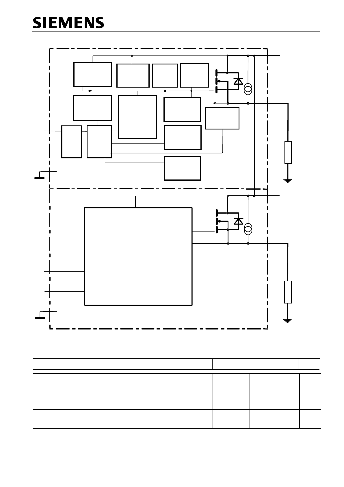
Block diagram
Voltage
source
Voltage
sensor
IN1
3
ESD
ST1
4
V
Logic
Logic
Overvoltage
protection
Charge pump
Level shifter
Rectifier
Current
limit
Limit for
unclamped
ind. loads
Open load
detection
Gate
protection
Temperature
sensor
+ V
bb
OUT1
BTS 707
Leadframe
17,18
Load
SignalGND
Chip 1
SignalGND
Chip 2
1
7
8
6
GND1
IN2
ST2
GND2
Short circuit
detection
Chip 1
Logic and protection circuit of chip 2
(equivalent to chip 1)
Chip 2
PROFET
Leadframe connected to pin 1, 10, 11, 12, 15, 16, 19, 20
+ V
bb
OUT2
Load GND
Leadframe
13,14
Load
Load GND
Maximum Ratings
at
= 25°C unless otherwise specified
j
T
Parameter Symbol Values Unit
Supply voltage (overvoltage protection see page 4)
Supply voltage for full short circuit protection
T
= -40 ...+150°C
j,start
Load current (Short-circuit current, see page 5)
Operating temperature range
Storage temperature range
V
V
I
T
T
bb
bb
L
j
stg
self-limited A
-40 ...+150
-55 ...+150
65 V
40 V
°C
Semiconductor Group 2
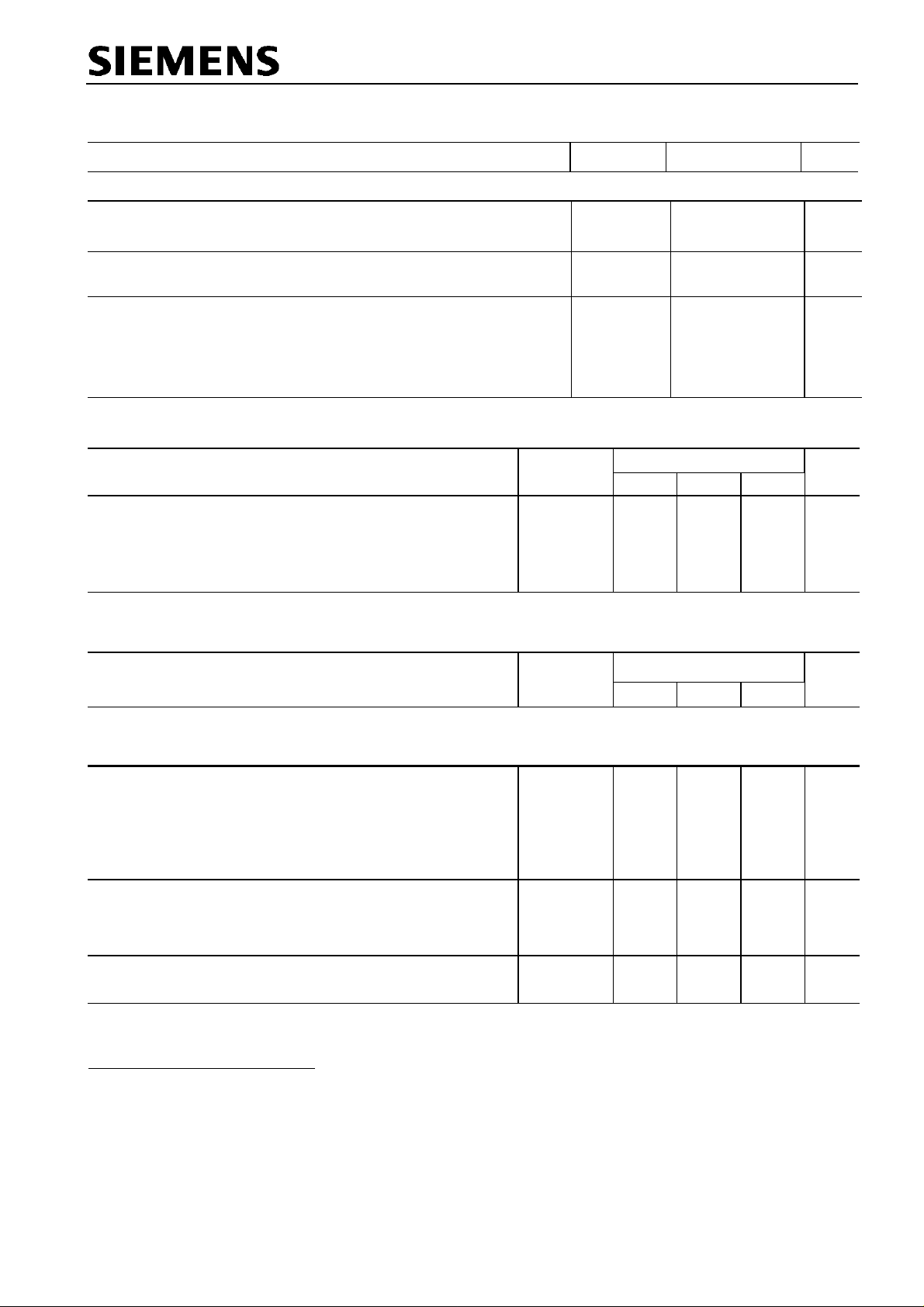
BTS 707
)
at
T
Maximum Ratings
Parameter Symbol Values Unit
= 25°C unless otherwise specified
j
Power dissipation (DC)
(all channels active)
Electrostatic discharge capability (ESD
(Human Body Model) all other pins:
Input voltage (DC)
Current through input pin (DC)
Current through status pin (DC)
see internal circuit diagram page 7
2)
T
= 25°C:
a
T
= 85°C:
a
IN, ST:
P
V
tot
ESD
1.6
1.0
3
W
kV
tbd (>1.0)
V
I
I
IN
IN
ST
-0.5 ... +36 V
±2.0
mA
±5.0
Thermal Characteristics
Parameter and Conditions Symbol Values Unit
min typ max
Thermal resistance
junction - soldering point
junction - ambient
2)
2),3)
each channel:
one channel active:
all channels active:
R
R
thjs
thja
-- -- 18
--
--
45
37
K/W
--
--
Electrical Characteristics
Parameter and Conditions,
at Tj = 25 °C,
V
= 12 V unless otherwise specified
bb
each of the two channels
Symbol Values Unit
Load Switching Capabilities and Characteristics
On-state resistance (Vbb to OUT)
IL = 2 A each channel,
V
= 24 V
bb
two parallel channels,
Nominal load current one channel active:
T
= 25°C:
j
T
= 150°C:
j
T
= 25°C:
j
R
ON
I
L(NOM)
two parallel channels active:
Device on PCB2),
Output current while GND disconnected or pulled
up; V
)
2
Device on 50mm*50mm*1.5mm epoxy PCB FR4 with 6cm
connection. PCB is vertical without blown air. See page 12
)
3
Soldering point: upper side of solder edge of device pin 15. See page 12
= 32 V,
bb
T
= 85°C,
a
V
= 0, see diagram page 8
IN
T
≤ 150°C
j
I
L(GNDhigh)
2
(one layer, 70µm thick) copper area for V
min typ max
--
1.60
2.4
225
400
113
1.9
2.8
250
500
125
-- A
-- -- 1.1 mA
mΩ
bb
Semiconductor Group 3

BTS 707
j
Parameter and Conditions,
at Tj = 25 °C,
Turn-on time
V
= 12 V unless otherwise specified
bb
each of the two channels
to 90%
Turn-off time to 10%
R
= 12
L
V
,
= 20 V
bb
Ω
T
=-40...+150°C
,
j
Slew rate on
10 to 30%
V
OUT
R
= 12
,
L
V
,
= 20 V
bb
T
=-40...+150°C:
j
,
Ω
Slew rate off
70 to 40%
V
OUT
,
R
= 12
L
V
,
= 20 V
bb
T
=-40...+150°C:
j
,
Ω
Operating Parameters
)
Operating voltage
Undervoltage shutdown
Undervoltage restart
4
T
=-40...+150°C:
j
T
=-40...+150°C:
j
T
=-40...+150°C:
j
Undervoltage restart of charge pump
see diagram page 11
T
=-40...+150°C:
j
Undervoltage hysteresis
V
∆
bb(under)
Overvoltage protection
I
= 40 mA
bb
=
V
bb(u rst)
-
V
bb(under)
)
5
T
=-40...+150°C:
j
Standby current, all channels off
V
= 0
IN
Operating current 6),
I
=
I
+
GND
GND1
I
GND2
V
= 5V,
IN
,
=-40...+150°C
T
T
=150°C:
j
one channel on:
two channels on:
V
V
OUT
OUT
Symbol Values Unit
min typ max
:
:
t
on
t
off
dV/dt
-dV/dt
V
bb(on)
V
bb(under)
V
bb(u rst)
V
bb(ucp)
V
∆
bb(under)
V
bb(AZ)
I
bb(off)
on
off
15
20
--
--
80
70
-- -- 6 V/µs
-- -- 7 V/µs
5.8 --
2.7 --
58 V
4.7 V
-- -- 4.9 V
-- 5.6 7.5 V
-- 0.4 -- V
65 70 -- V
--
20 70
--
I
GND
--
--
2.2
4.4
µ
A
µ
----mA
s
Protection Functions
Initial peak short circuit current limit,
diagrams, page 9)
each channel,
two parallel channels
Output clamp (inductive load switch off)
at V
ON(CL)
= Vbb - V
OUT
Thermal overload trip temperature
Thermal hysteresis
4)
At supply voltage increase up to
5)
see also
)
6
Add
)
7
If channels are connected in parallel, output clamp is usually accomplished by the channel with the lowest
V
ON(CL)
V
, if
I
ST
in circuit diagram on page 7.
ON(CL)
> 0
I
ST
(see timing
=-40°C:
j
T
=25°C:
j
T
=+150°C:
j
T
7)
I
V
T
∆T
= 5.6 V typ without charge pump,
V
bb
L(SCp)
ON(CL)
jt
jt
--
--
4.0
--
10
--
twice the current of one channel
59 -- 75 V
150 -- -- °C
-- 10 -- K
≈
V
OUT
V
bb
- 2 V
Semiconductor Group 4
19
A
--
--
 Loading...