

Siemens BTS612N1 Datasheet
Smart Two Channel Highside Power Switch
)
)
)
)
BTS 612 N1
Features
•
Overload protection
•
Current limitation
•
Short circuit protection
•
Thermal shutdown
•
Overvoltage protection (including load dump)
•
Fast demagnetization of inductive loads
•
Reverse battery protection
•
Undervoltage and overvoltage shutdown with
1
)
auto-restart and hysteresis
•
Open drain diagnostic output
•
Open load detection in OFF-state
•
CMOS compatible input
•
Loss of ground and loss of
•
Electrostatic discharge (ESD) protection
V
protection
bb
Application
•
µC compatible power switch with diagnostic
Product Summary
Overvoltage protection
Operating voltage
channels: each
On-state resistance
Load current (ISO)
Current limitation
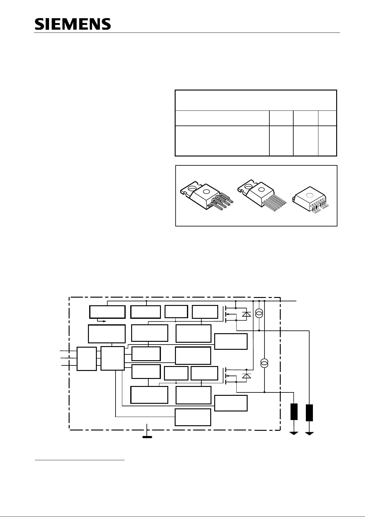
TO-220AB/7
7
1
Standard
Straight leads
R
ON
I
L(ISO
I
L(SCr
V
bb(AZ
V
bb(on
1
43 V
5.0 ... 34 V
both
parallel
200 100
2.3 4.4 A
44A
7
1
SMD
feedback for 12 V and 24 V DC grounded loads
•
All types of resistive, inductive and capacitve loads
•
Replaces electromechanical relays, fuses and discrete circuits
General Description
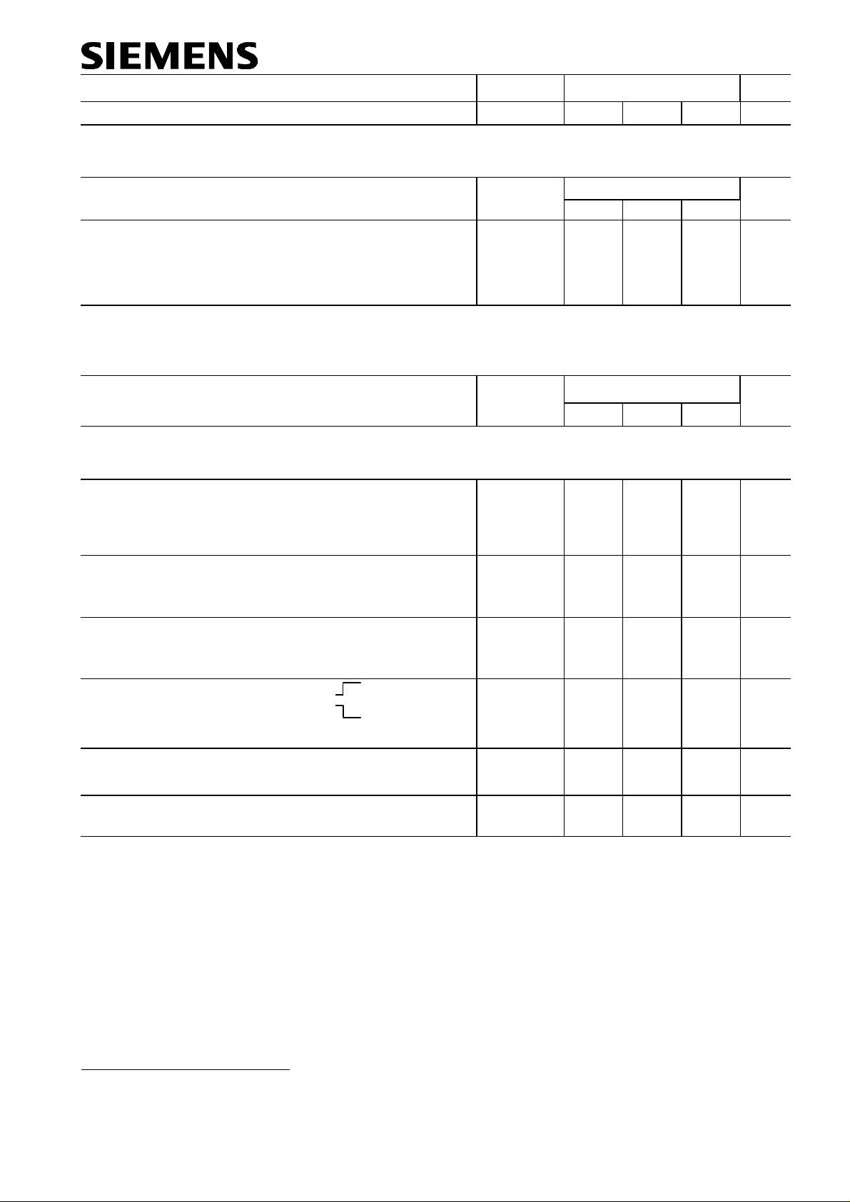
N channel vertical power FET with charge pump, ground referenced CMOS compatible input and diagnostic
feedback, monolithically integrated in Smart SIPMOS technology. Fully protected by embedded protection
functions.
m
Ω
7
Voltage
source
V
Logic
Voltage
sensor
3
IN1
IN2
6
ESD
5
ST
PROFET
Logic
Overvoltage
protection
Level shifter
Rectifier 1
Charge
pump 1
Charge
pump 2
Level shifter
Rectifier 2
GND
2
Current
limit 1
Current
limit 2
Signal GND
)
1
With external current limit (e.g. resistor R
=150 Ω) in GND connection, resistor in series with ST
GND
connection, reverse load current limited by connected load.
Gate 1
protection
Limit for
unclamped
ind. loads 1
Open load
Short to Vbb
detection 1
Gate 2
protection
Limit for
unclamped
ind. loads 2
Open load
Short to Vbb
detection 2
Temperature
sensor 1
Temperature
sensor 2
+ V
OUT1
OUT2
bb
4
1
7
Load
Load GND
Semiconductor Group 1
BTS 612 N1
j,
Parameter and Conditions,
at
T
= 25 °C,
j
V
= 12 V unless otherwise specified
bb
each channel
Symbol Values Unit
min typ max
Pin Symbol Function
1 OUT1 (Load, L) Output 1, protected high-side power output of channel 1
2 GND Logic ground
3 IN1 Input 1, activates channel 1 in case of logical high signal
4V
bb
Positive power supply voltage,
the tab is shorted to this pin
5ST
Diagnostic feedback: open drain, low on failure
6 IN2 Input 2, activates channel 2 in case of logical high signal
7 OUT2 (Load, L) Output 2, protected high-side power output of channel 2
at
T
= 25 °C unless otherwise specified
Maximum Ratings
j
Parameter Symbol Values Unit
Supply voltage (overvoltage protection see page 4)
Supply voltage for full short circuit protection
T
=-40 ...+150°C
j Start
)
Load dump protection
)
3
R
= 2 Ω,
I
R
= 5.3 Ω,
L
2
V
LoadDump
t
= 200 ms, IN= low or high
d
=
U
A
+
V
,
s
U
= 13.5 V
A
Load current (Short circuit current, see page 5)
Operating temperature range
Storage temperature range
Power dissipation (DC), TC ≤ 25 °C
V
bb
V
bb
V
Load dump
I
L
T
j
T
stg
P
tot
43 V
34 V
)
4
60 V
self-limited A
-40 ...+150
°C
-55 ...+150
36 W
Inductive load switch-off energy dissipation, single pulse
V
= 12V,
one channel,
both channels parallel,
see diagrams on page 9
Electrostatic discharge capability (ESD) IN:
(Human Body Model) all other pins:
acc. MIL-STD883D, method 3015.7 and ESD assn. std. S5.1-1993
Input voltage (DC)
Current through input pin (DC)
Current through status pin (DC)
see internal circuit diagrams page 8
T
= 150°C,
start
T
= 150°C const.
C
I
= 2.3 A, Z
L
I
= 4.4 A, Z
L
= 89 mH, 0
L
= 47 mH, 0 Ω: 580
L
Ω
:
E
AS
V
ESD
V
I
I
IN
IN
ST
-10 ... +16 V
290 mJ
1.0
2.0
±
±
2.0
5.0
mA
kV
)
2
Supply voltages higher than V
150 Ω resistor in the GND connection and a 15 kΩ resistor in series with the status pin. A resistor for the
protection of the input is integrated.
3)
R
= internal resistance of the load dump test pulse generator
I
4)
V
Load dump
is setup without the DUT connected to the generator per ISO 7637-1 and DIN 40839
require an external current limit for the GND and status pins, e.g. with a
bb(AZ)
Semiconductor Group 2
BTS 612 N1
Parameter and Conditions,
at
T
= 25 °C,
j
V
= 12 V unless otherwise specified
bb
each channel
Symbol Values Unit
min typ max
Thermal Characteristics
Parameter and Conditions Symbol Values Unit
min typ max
Thermal resistance chip - case, both channels:
each channel:
junction - ambient (free air):
R
R
thJC
thJA
--
--
--
--
--
--
3.5
7.0
75
K/W
SMD version, device on PCB5):37
Electrical Characteristics
Parameter and Conditions,
at
T
= 25 °C,
j
V
= 12 V unless otherwise specified
bb
Load Switching Capabilities and Characteristics
On-state resistance (pin 4 to 1 or 7)
I
= 1.8 A
L
each channel
Nominal load current, ISO Norm (pin 4 to 1 or 7)
V
= 0.5 V,
ON
T
= 85 °C each channel:
C
Output current (pin 1 or 7) while GND disconnected
or GND pulled up,
V
bb
=30 V,
page 9
Turn-on time IN to 90%
Turn-off time IN to 10%
R
= 12
L
T
=-40...+150°C
Ω
,
j
Slew rate on
10 to 30%
V
OUT
R
= 12
,
L
Slew rate off
70 to 40%
V
OUT
,
R
= 12
L
each channel
T
=25 °C:
j
T
=150 °C:
j
both channels parallel:
V
= 0, see diagram
IN
T
=-40...+150°C
Ω
,
j
T
=-40...+150°C
Ω
,
j
V
V
OUT
OUT
Symbol Values Unit
min typ max
R
:
:
I
I
t
t
dV /dt
-dV/dt
ON
L(ISO)
L(GNDhigh)
on
off
on
off
-- 160
1.8
3.5
320
2.3
4.4
200
400
-- -- 10 mA
80
80
200
200
400
400
0.1 -- 1 V/µs
0.1 -- 1 V/µs
m
Ω
--
A
--
µ
s
)
5
Device on 50mm*50mm*1.5mm epoxy PCB FR4 with 6cm
connection. PCB is vertical without blown air.
Semiconductor Group 3
2
(one layer, 70µm thick) copper area for V
bb
BTS 612 N1
j
j
j
Parameter and Conditions,
at
T
= 25 °C,
j
V
= 12 V unless otherwise specified
bb
each channel
Operating Parameters
)
Operating voltage
Undervoltage shutdown
Undervoltage restart
6
T
j
T
j
T
Undervoltage restart of charge pump
see diagram page 12
Undervoltage hysteresis
V
∆
bb(under)
Overvoltage shutdown
Overvoltage restart
Overvoltage hysteresis
Overvoltage protection
I
bb
Standby current (pin 4)
V
IN
Operating current (Pin 2)8),
both channels on,
Operating current (Pin 2)
one channel on,
=
=40 mA
=0
V
bb(u rst)
-
V
bb(under)
)
7
,
V
=5 V
IN
=-40...+150°C,
T
8)
=-40...+150°C:,
T
T
j
T
j
T
j
T
j
T
=-40...+150°C:
=-40...+150°C:
=-40...+25°C:
T
=+150°C:
j
=-40...+150°C:
=-40...+150°C:
=-40...+150°C:
=-40...+150°C:
=-40...+150°C:
j
Symbol Values Unit
min typ max
V
bb(on)
V
bb(under)
V
bb(u rst)
5.0 -- 34 V
3.5 -- 5.0 V
-- -- 5.0
7.0
V
bb(ucp)
V
∆
V
bb(over)
V
bb(o rst)
V
∆
V
bb(AZ)
I
bb(off)
bb(under)
bb(over)
-- 5.6 7.0 V
-- 0.2 -- V
34 -- 43 V
33 -- -- V
-- 0.5 -- V
42 47 -- V
-- 90 150
I
GND
I
GND
-- 0.6 1.2 mA
-- 0.4 0.7 mA
V
A
µ
6)
At supply voltage increase up to
7)
)
8
See also
Add
V
I
, if
ST
in table of protection functions and circuit diagram page 8.
ON(CL)
I
> 0, add
ST
I
IN
, if
V
= 5.6 V typ without charge pump,
bb
V
>5.5 V
IN
Semiconductor Group 4
V
OUT
≈
V
- 2 V
bb
BTS 612 N1
j
j
)
Parameter and Conditions,
at
T
= 25 °C,
j
V
= 12 V unless otherwise specified
bb
each channel
Protection Functions
Initial peak short circuit current limit (pin 4 to 1
or 7)
=-40°C:
T
=25°C:
T
=+150°C:
j
T
Repetitive short circuit shutdown current limit
T
=
T
j
(see timing diagrams, page 11)
jt
Output clamp (inductive load switch off)
at
V
=
V
-
OUT
bb
V
ON(CL)
I
= 40 mA:
L
Thermal overload trip temperature
Thermal hysteresis
)
Reverse battery (pin 4 to 2)
Reverse battery voltage drop
= -1.9 A, each channel
I
L
9
(V
out
> V
bb
)
T
=150 °C:
j
Symbol Values Unit
min typ max
I
L(SCp)
I
L(SCr)
5.5
4.5
2.5
9.5
7.5
4.5
13
11
7
-- 4 -- A
V
ON(CL)
T
jt
∆T
-
V
-V
jt
bb
ON(rev)
41 47 53 V
150 -- -- °C
-- 10 -- K
-- -- 32 V
--
610 --
mV
A
Diagnostic Characteristics
Open load detection current
(included in standby current
I
bb(off
Open load detection voltage
I
)
=-40..150°C:
T
j
L(off)
V
OUT(OL)
-- 30 --
A
µ
234V
)
9
Requires 150 Ω resistor in GND connection. The reverse load current through the intrinsic drain-source
diode has to be limited by the connected load. Note that the power dissipation is higher compared to normal
operating conditions due to the voltage drop across the intrinsic drain-source diode. The temperature
protection is not active during reverse current operation! Input and Status currents have to be limited (see
max. ratings page 2 and circuit page 8).
Semiconductor Group 5
 Loading...