

Siemens BTS555 Datasheet
PROFET® Target Data Sheet BTS555
)
)
)
)
Smart Highside High Current Power Switch
Features
•
Overload protection
•
Current limitation
•
Short circuit protection
•
Overtemperature protection
•
Overvoltage protection (including load dump)
•
Clamp of negative voltage at output
•
Fast deenergizing of inductive loads
•
Low ohmic inverse current operation
•
Reverse battery protection
•
Diagnostic feedback with load current sense
•
Open load detection via current sense
•
Loss of
•
Electrostatic discharge (ESD) protection
V
protection
bb
2)
1)
Product Summary
Overvoltage protection
Output clamp
Operating voltage
On-state resistance
Load current (ISO)
Short circuit current limitation
Current sense ratio
Application
•
Power switch with current sense diagnostic
feedback for 12
•
Most suitable for loads with high inrush current
like lamps and motors; all types of resistive and
inductive loads
•
Replaces electromechanical relays, fuses and discrete circuits
V and 24 V DC grounded loads
V
bb(AZ
V
ON(CL
V
bb(on
R
ON
I
L(ISO
I
L(SCp)
I
L :
TO-218AB/5
1
Straight leads
63 V
42
V
5.0 ... 34 V
2.9
mΩ
132 A
400 A
I
IS
25 000
5
General Description
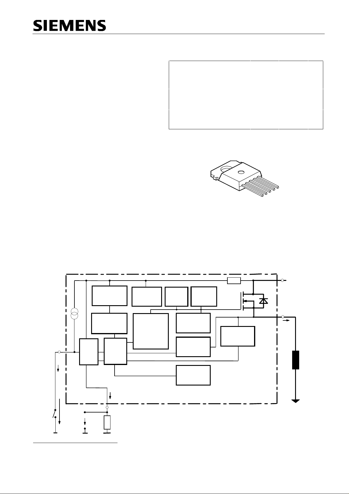
N channel vertical power FET with charge pump, current controlled input and diagnostic feedback with load
current sense, integrated in Smart SIPMOS chip on chip technology. Fully protected by embedded protection
functions.
3 & Tab
+ V
R
Voltage
source
Voltage
sensor
2
IN
ESD
I
IN
V
IN
V
IS
Logic
I
IS
IS
4
R
IS
Overvoltage
protection
Charge pump
Level shifter
Rectifier
Current
limit
Gate
protection
Limit for
unclamped
ind. loads
Output
Voltage
detection
Temperature
sensor
bb
Current
Sense
PROFET
bb
OUT
1, 5
I
L
Load GND
Load
Logic GND
1
) With additional external diode.
2)
Additional external diode required for energized inductive loads (see page 9).
Semiconductor Group Page 1 of 16 1998-Jan-14
Target Data Sheet BTS555
T
T
j,
T
)
)
Pin Symbol Function
1 OUT O
2 IN I Input, activates the power switch in case of short to ground
3V
4ISS
5 OUT O
bb
Output to the load. The pins
especially in high current applications!
Positive power supply voltage, the tab is electrically connected to this pin.
+
In high current applications the tab should be used for the V
instead of this pin
Diagnostic feedback providing a sense current proportional to the load
current; zero current on failure (see Truth Table on page 7)
Output to the load. The pins
especially in high current applications!
4)
.
1 and 5 must be shorted with each other
3)
1 and 5 must be shorted with each other
3)
connection
bb
Maximum Ratings at
T
j = 25 °C unless otherwise specified
Parameter Symbol Values Unit
Supply voltage (overvoltage protection see page 4)
Supply voltage for full short circuit protection,
resistive load or L < tbd µH
=-40 ...+150°C:
j,start
Load current (short circuit current, see page 5)
Load dump protection
5)
R
= 2 Ω,
I
R
= 0.1 Ω,
L
V
LoadDump
t
= 200 ms,
d
=
U
A
+
V
,
s
U
= 13.5 V
A
V
bb
V
bb
I
L
V
Load dump
42 V
34 V
self-limited A
)
6
80 V
IN, IS = open or grounded
Operating temperature range
Storage temperature range
Power dissipation (DC), TC ≤ 25 °C
T
T
P
j
stg
tot
-40 ...+150
-55 ...+150
310 W
°C
Inductive load switch-off energy dissipation, single pulse
V
= 12V,
I= tbd (>=20
page 10
Electrostatic discharge capability (ESD
Human Body Model acc. MIL-STD883D, method 3015.7 and ESD
assn. std. S5.1-1993, C = 100 pF, R = 1.5 kΩ
Current through input pin (DC)
Current through current sense status pin (DC)
see internal circuit diagrams on page 8
start
A, Z
= 150°C,
= 150°C const.,
C
= tbd mH, 0 Ω, see diagrams on
E
V
I
I
AS
ESD
IN
IS
tbd J
2.0 kV
+15 , -250
+15 , -250
mA
3)
Not shorting all outputs will considerably increase the on-state resistance, reduce the peak current
capability and decrease the current sense accuracy
4)
Otherwise add up to 0.5 mΩ (depending on used length of the pin) to the RON if the pin is used instead of
the tab.
5)
R
= internal resistance of the load dump test pulse generator.
I
6)
V
Load dump
is setup without the DUT connected to the generator per ISO 7637-1 and DIN 40839.
Semiconductor Group Page 2 1998-Jan-14
Thermal Characteristics
Symbol
V
T
I
I
I
Target Data Sheet BTS555
Parameter and Conditions
Values Unit
min typ max
Thermal resistance chip - case:
junction - ambient (free air):
R
R
thJC
thJA
-- -- 0.40
--
30 --
K/W
)
7
Electrical Characteristics
Parameter and Conditions Symbol Values Unit
at
T
j = -40 ... +150 °C,
Load Switching Capabilities and Characteristics
On-state resistance (Tab to pins 1,5, see measurement
circuit page 8)
Nominal load current9) (Tab to pins 1,5)
ISO 10483-1/6.7:
Maximum load current in resistive range
(Tab to pins 1,5)
see diagram on page 13
Turn-on time
11)
Turn-off time IIN to 10%
R
= 1 Ω ,
L
Slew rate on
R
= 1 Ω
L
Slew rate off
R
= 1 Ω
L
T
=-40...+150°C
j
11)
11)
V
= 12 V unless otherwise specified
bb
I
V
IN
V
= 0,
I
L
= tbd V8),
bb
V
ON
= tbd (>=20) A,
L
= tbd (>=20) A,
I
= tbd A,
L
I
= tbd A,
L
= 0.5 V,
V
ON
T
c
= 1.8 V,
ON
= 1.8 V,
= 85 °C
T
= 25 °C:
j
T
= 150 °C:
j
T
= 150 °C: tbd tbd
j
T
= 150 °C:
j
10)
= 25 °C:
c
T
= 150 °C:
c
IIN to 90%
(10 to 30%
(70 to 40%
V
V
OUT
OUT
)
)
V
V
OUT
OUT
:
:
R
ON
R
ON(Static)
I
L(ISO)
L(Max)
t
on
t
off
dV/dt
-dV/dt
on
off
min typ max
-- 2.4
4.6
2.9
5.7
mΩ
-- tbd tbd
111 132 -- A
tbd
tbd
130
60
--
--
--
--
--
--
550
240
A
µs
-- 0.8 -- V/µs
-- 0.8 -- V/µs
Inverse Load Current Operation
On-state resistance (Pins 1,5 to pin 3)
V
= 12 V,
bIN
see diagram on page 10
Nominal inverse load current (Pins 1,5 to Tab)
V
= -0.5 V,
ON
Drain-source diode voltage (V
-
=
tbd (>=20) A,
L
7)
Thermal resistance R
8)
Decrease of V
long as V
9)
Not tested, specified by design.
10)
T
is about 105°C under these conditions.
J
11)
See timing diagram on page 14.
I
= - tbd (>=20) A
L
T
= 85 °C
c
below 10 V causes slowly a dynamic increase of RON to a higher value of R
bb
> V
bIN
bIN(u) max
10
> Vbb)
out
= 0,
T
IN
thCH
j = +150°C
case to heatsink (about 0.25 K/W with silicone paste) not included!
, RON increase is less than 10 % per second for TJ < 85 °C.
T
= 25 °C:
j
T
= 150 °C:
j
R
ON(inv)
I
L(inv)
-
V
111 132 -- A
ON
-- 2.4
4.6
2.9
5.7
mΩ
-- tbd -- mV
ON(Static)
. As
Semiconductor Group Page 3 1998-Jan-14

Target Data Sheet BTS555
(
V
V
V
V
t
I
(
)
I
)
V
V
V
)
)
I
V
V
Parameter and Conditions Symbol Values Unit
at
T
j = -40 ... +150 °C,
Operating Parameters
Operating voltage
12
)
Undervoltage shutdown
Undervoltage start of charge pump
see diagram page 15
Overvoltage protection
I
= 15 mA
bb
Standby current
I
= 0
IN
Protection Functions
Short circuit current limit (Tab to pins 1,5)
V
= 12 V, time until shutdown max. 300 µs
ON
Short circuit shutdown delay after input current
positive slope,
min. value valid only if input "off-signal" time exceeds 30 µs
Output clamp
inductive load switch off
Output clamp (inductive load switch off
at
= 40 mA
L
OUT
=
bb
Short circuit shutdown detection voltage
(pin 3 to pins 1,5)
15)
-
ON
ON(CL
V
= 12 V unless otherwise specified
bb
Fehler! Textmarke nicht definiert.,
= 0)
IN
13)
14)
T
T
= 25...+150°C:
j
T
=-40...+25°C:
j
T
T
T
T
=+150°C:
c
>
ON(SC)
L
(e.g. overvoltage
=-40°C:
j
= 150°C:
j
=-40°C:
c
=25°C:
c
= 40 mA:
= 20 A:
L
V
bb(on)
V
bIN(u)
bIN(ucp)
V
bIN(Z)
I
bb(off)
I
L(SCp)
d(SC)
-
V
OUT(CL)
ON(CL)
ON(SC)
min typ max
5.0 -- 34 V
-- 3.5 4.5 V
-- 5 6.5 V
60
62
--
--
-tbd
tbd
--
66
15
25
460
400
280
--
--
25
60
-tbd
tbd
µA
80 -- 300 µs
--
--
15
17
--
--
39 42 46 V
-- 6 -- V
V
A
V
12)
For all voltages 0 ... 34 V the device is fully protected against overtemperature and short circuit.
13)
14)
15)
= V
- V
V
bIN
(typ.) the charge pump is not active and
See also
This output clamp can be "switched off" by using an additional diode at the IS-Pin (see page 8). If the diode
is used, V
bb
see diagram on page 8. When
IN
V
OUT
in circuit diagram on page 9.
ON(CL)
is clamped to Vbb- V
V
at inductive load switch off.
ON(CL)
OUT
V
increases from less than V
bIN
≈
V
- 3 V.
bb
bIN(u)
up to
V
bIN(ucp)
= 5 V
Semiconductor Group Page 4 1998-Jan-14
Target Data Sheet BTS555
V
V
I
)
R
T
j
k
I
I
,
V
V
V
V
I
I
50
I
25
I
10
)
)
Parameter and Conditions Symbol Values Unit
at
T
j = -40 ... +150 °C,
V
= 12 V unless otherwise specified
bb
min typ max
Thermal overload trip temperature
Thermal hysteresis ∆
Reverse Battery
Reverse battery voltage
On-state resistance (Pins 1,5 to pin 3)
= -12V,
bb
IN
= 0,
16)
= - tbd (>=20
L
A,
= 1 kΩ
IS
T
= 25 °C:
j
=
150 °C:
Integrated resistor in Vbb line
Diagnostic Characteristics
Current sense ratio, static on-condition, -40°C:
=
ILIS
<
IS
:
L
IS
- 5 ??? V,
OUT
< 1.5 V
ON
see diagram on page 12
I
= 0 (e.g. during deenergizing of inductive loads):
IN
17)
, 25°C:
> 4.5 V 150°C:
bIN
= 180 A:
L
=
L
=
L
=
L
A:
A:
A:
T
jt
T
-
V
R
ON(rev)
R
bb
k
ILIS
bb
150 -- -- °C
jt
-- 10 -- K
-- -- 16 V
--
2.8
-- 120 --
--
26 530
--
25 430
--
23 520
-40°C:
±4.5%
±8.9%
±15%
±46%
+25°C:
±4.2%
±7.5%
±12%
±36%
0
tbd
0
--
--
--
150°C:
±4.0%
±6.1%
±9.0%
±24%
mΩ
Ω
-- 0 --
Sense current saturation
I
IS,lim
6.5 -- -- mA
Current sense leakage current
I
= 0,
V
IN
V
= 0,
V
IN
Current sense settling time
slope (90% of
I
static)
IS
Current sense settling time
slope (10% of
I
static)
IS
Current sense settling time
current (60% to 90%)
Overvoltage protection
I
= 15 mA
bb
16)
The reverse load current through the intrinsic drain-source diode has to be limited by the connected load
(as it is done with all polarity symmetric loads). Note that under off-conditions (
transistor is not activated. This results in raised power dissipation due to the higher voltage drop across the
intrinsic drain-source diode. The temperature protection is not active during reverse current operation!
Increasing reverse battery voltage capability is simply possible as described on page 9.
17)
If VON is higher, the sense current is no longer proportional to the load current due to sense current
I
saturation, see
18)
Not tested, specified by design.
IS,lim
.
18)
after positive input
I
= 0 / tbd (>=20) A:
L
18)
after negative input
I
= tbd (>=20) / 0 A:
L
18)
after change of load
I
= 15 / tbd (>=20) A:
L
T
= 0,
IS
T
= 25...+150°C:
j
= 0:
IS
I
L
=-40°C:
j
≤ 0:
I
IS(LL)
I
IS(LH)
t
son(IS
t
soff(IS
t
slc(IS)
V
bIS(Z)
--
--
-2
-- tbd 500
-- tbd 500
-- tbd 500
60
62
I
IN
--
66
=
I
= 0) the power
IS
0.5
--
--
--
µA
µs
µs
µs
V
Semiconductor Group Page 5 1998-Jan-14
 Loading...