

Siemens BTS550P Datasheet
PROFET® Preliminary Data Sheet BTS550P
)
Smart Highside High Current Power Switch
Features
•
Overload protection
•
Current limitat ion
•
Short circuit pr otection
•
Overtemperature protection
•
Overvoltage protection (including load dump)
•
Clamp of negative volt age at output
•
Fast deenergizing of induc tive loads
•
Low ohmic inverse current operation
•
Reverse battery pr otection
•
Diagnostic feedback with load current sense
•
Open load detection via c ur r ent sense
•
Loss of
•
Electrostatic discharge (ESD) protection
V
protection
bb
2)
1)
Application
•
Power switch with c ur r ent sense diagnostic
feedback for 12
•
Most suitable f or loads with high inrush current
like lamps and motors; all types of res is tive and
inductive loads
•
Replaces electromechanic al r elay s , fuses and
discrete circuits
V and 24 V DC grounded loads
Product Summary
Overvoltage protection
Output clamp
Operating voltage
On-state resistance
Load current (ISO)
Short circuit current l i m i t ation
Current sense ratio
TO-218AB/5
Straight leads
V
bb(AZ)
V
ON(CL
V
bb(on)
R
ON
I
L(ISO)
I
L(SCp)
I
L :
1
63 V
42
V
5.0 ... 34 V
4.0
mΩ
97 A
180 A
I
IS
21000
5
General Description
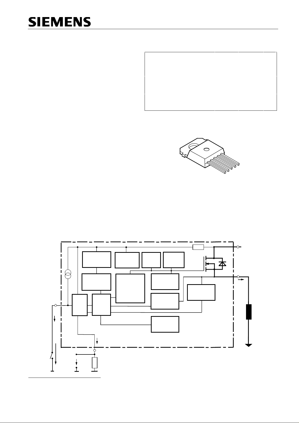
N channel vertical power F E T with charge pump, c ur r ent controlled input and diagnos tic feedback with load
current sense, integrated in Smart S IPMOS chip on chip technology. Fully protected by em bedded pr otection
functions.
3 & Tab
+ V
R
Voltage
source
Voltage
sensor
2
IN
ESD
I
IN
V
IN
V
IS
Logic
I
IS
IS
4
R
IS
Overvoltage
protection
Charge pump
Level shifter
Rectifier
Current
limit
Gate
protection
Limit for
unclamped
ind. loads
Output
Voltage
detection
Temperature
sensor
bb
Current
Sense
PROFET
bb
OUT
1, 5
I
L
Load GND
Load
Logic GND
1
) With additional ext er nal diode.
2)
Additional external diode requir ed for energized inductive loads ( s ee page 8) .
Semiconductor Group Page 1 of 15 1998-Aug-31
Preliminary Data Sheet BTS550P
Pin Symbol Function
1OUTO
2 IN I Input, act iv ates the power switc h in c as e of short to gr ound
3V
4ISS
5OUTO
bb
Output to the load. The pins
especially in high current applic ations!
Positive power supply v oltage, the tab is elec trically connect ed to this pin.
+
In high current applications the tab should be used for the V
4)
instead of this pin
Diagnostic feedback pr ov iding a s ens e c ur r ent proportional to t he load
current; zer o c ur r ent on failure (see Tr uth Table on page 6)
Output to the load. The pins
especially in high current applic ations!
.
1 and 5 must be shorted with each other
3)
1 and 5 must be shorted with each other
3)
connection
bb
Maximum Ratings at
T
j = 25 °C unless otherwise specified
Parameter Symbol Values Unit
Supply voltage (overvoltage protection see page 4)
Supply voltage for full short circuit protection,
T
=-40 ...+150°C:
j,start
Load current (short circuit current, see page 4)
Load dump protection
5)
R
= 2 Ω,
I
R
= 0.54 Ω,
L
V
LoadDump
t
= 200 ms,
d
=
U
A
+
V
s
,
U
= 13.5 V
A
V
bb
V
bb
I
L
V
Load dump
42 V
34 V
self-limited A
)
6
90 V
IN, IS = open or grounded
Operating temperature range
Storage temperature range
Power dissipation (DC), TC ≤ 25 °C
T
T
P
j
stg
tot
-40 ...+150
-55 ...+150
360 W
°C
Inductive load switch-off energy dissipation, single pulse
V
= 12V,
bb
I
= 20 A, ZL = 15 mH, 0 Ω, see diagrams on page 9
L
Electrostatic discharge capability (ESD)
Human Body Model acc. M IL-STD883D, method 3015.7 and ESD
assn. std. S 5.1-1993, C = 100 pF , R = 1.5 kΩ
Current through input pin (DC)
Current through current sense status pin (DC)
see internal circuit diagr am s on page 6 and 7
T
j,start
= 150°C,
T
= 150°C const.,
C
E
V
I
I
AS
ESD
IN
IS
+15 , -250
+15 , -250
3J
4kV
mA
3)
Not shorting all outputs will considerably increas e the on-state r es is tance, reduce the peak c ur r ent
capability and decrease t he c ur r ent sense accuracy
4)
Otherwise add up to 0.5 mΩ (depending on used length of t he pin) to the RON if the pin is used inst ead of
the tab.
5)
R
= internal resis tance of the load dump t es t pulse generator.
I
6)
V
Load dump
is setup without the DUT connected t o the generator per I S O 7637-1 and DIN 40839.
Semiconductor Group Page 2 1998-Aug-31
Preliminary Data Sheet BTS550P
Thermal Characteristics
Parameter and Conditions Symbol Values Unit
min typ max
)
7
Thermal resistance chip - case:
junction - ambient (free air):
R
R
thJC
thJA
-- -- 0.35
--
30 --
K/W
Electrical Characteristics
Parameter and Conditions Symbol Values Unit
at
T
j = -40 ... +150 °C,
Load Switching Capabilities and Characteristics
On-state resistance (Tab to pins 1,5, s ee m eas ur em ent
circuit page 6)
Nominal load current9) (Tab to pins 1, 5)
ISO 10483-1/6.7:
Maximum load current in resistive range
(Tab to pins 1,5)
see diagram on page 12
Turn-on time
Turn-off time IIN to 10%
R
= 1 Ω ,
L
T
=-40...+150°C
j
Slew rate on
R
= 1 Ω ,
L
T
=25°C
j
Slew rate off
R
= 1 Ω ,
L
T
=25°C
j
V
= 12 V unless otherwis e s pec ified
bb
I
= 20 A,
L
V
= 0,
I
V
ON
V
V
I
L
I
ON
OUT
OUT
= 20 A,
L
= 120 A,
= 20 A,
L
T
= 85 °C
c
= 1.8 V,
= 1.8 V,
)
)
T
IN
V
= 6V8),
bb
V
= 0.5 V,
ON
V
11)
IIN to 90%
11)
(10 to 30%
11)
(70 to 40%
min typ max
T
= 25 °C:
j
T
= 150 °C:
j
T
= 150 °C: -- 8
j
T
= 150 °C:
j
10)
T
= 25 °C:
c
= 150 °C:
c
V
OUT
V
OUT
:
:
R
ON
R
ON(Static)
I
L(ISO)
I
L(Max)
t
on
t
off
dV/dt
-dV/dt
on
off
-- 3.3
6.4
-- 9 12
80 97 -- A
350
180
140
40
--
--
--
--
-- 0.45 -- V/µs
-- 0.55 -- V/µs
4.0
7.8
600
150
--
--
mΩ
A
µs
Inverse Load Current Operation
On-state resistance (Pins 1,5 to pin 3)
V
= 12 V,
bIN
see diagram on page 9
Nominal inverse load current (Pins 1,5 to Tab)
V
= -0.5 V,
ON
Drain-source diode voltage (V
I
-
=
20 A,
L
7)
Thermal resist anc e R
8)
Decrease of V
long as V
9)
Not tested, s pec ified by design.
10)
T
is about 105°C under thes e c onditions.
J
11)
See timing diagram on page 13.
I
bIN
IN
I
= - 20 A
L
T
= 85 °C
c
= 0,
below 10 V causes a slowly a dynamic inc r eas e of RON to a higher value of R
bb
> V
bIN(u) max
10
> V
out
T
j = +150°C
case to heatsink ( about 0.25 K/W with silicone paste) not included!
thCH
, RON increase is less than 10 % per s ec ond for TJ < 85 °C.
bb
T
)
T
= 25 °C:
j
= 150 °C:
j
R
ON(inv)
I
L(inv)
-
V
ON
-- 3.3
80 97 -- A
-- 0.8 -- V
6.4
4.0
7.8
ON(Static)
mΩ
. As
Semiconductor Group Page 3 1998-Aug-31

Preliminary Data Sheet BTS550P
I
I
Parameter and Conditions Symbol Values Unit
at
T
j = -40 ... +150 °C,
Operating Parameters
Operating voltage (
Undervoltage shutdown
Undervoltage start of charge pump
see diagram page 14
Overvoltage protection
I
= 15 mA
bb
Standby current
I
= 0
IN
Protection Functions
Short circuit current limit (Tab to pins 1,5)
V
= 12 V, time until shutdown max. 350 µs
ON
Short circuit shutdown delay after input current
positive slope,
min. value valid only if input "off-s ignal" time exceeds 30 µs
Output clamp
(inductive load switch off)
Output clamp (inductive load switch off)
at
V
=
V
bb
I
= 40 mA
L
OUT
Short circuit shutdown detection voltage
(pin 3 to pins 1,5)
Thermal overload trip temperature
Thermal hysteresis
15)
-
V
ON
V
ON(CL)
V
= 12 V unless otherwis e s pec ified
bb
= 0)
13)
14)
8, 12)
T
T
= 25...+150°C:
j
T
=-40...+25°C:
j
V
IN
T
T
T
T
=+150°C:
c
>
V
ON(SC)
L
(e.g. overvoltage)
=-40°C:
j
= 150°C:
j
=-40°C:
c
=25°C:
c
= 40 mA:
= 20 A:
L
V
bb(on)
V
bIN(u)
V
bIN(ucp)
V
bIN(Z)
I
bb(off)
I
L(SCp)
t
d(SC)
-
V
OUT(CL)
V
ON(CL)
V
ON(SC)
T
jt
∆
T
jt
min typ max
5.0 -- 34 V
2.0 3.0 4.5 V
3.5 4.5 6.0 V
60
62
--
--
--
--
120
--
66
15
25
170
180
170
25
50
250
--
--
--
--
V
µA
A
80 -- 350 µs
----16.8
19.0
--
--
V
39 42 46.5 V
-- 6 -- V
150 -- -- °C
-- 10 -- K
12)
If the device is turned on before a V
For the voltage r ange 0..34 V the device is fully protect ed agains t overtemperat ur e and s hor t circuit.
13)
14)
15)
= V
- V
V
bIN
(typ.) t he c har ge pum p is not active and
See also
This output clamp can be "switched off" by using an additional diode at the IS-Pin (see page 7). If the diode
is used, V
bb
see diagram on page 6. When
IN
V
OUT
in circuit diagram on page 7.
ON(CL)
is clamped to Vbb- V
-decrease, the oper ating voltage range is ext ended down to
bb
V
increases from les s than V
bIN
V
≈
V
OUT
at inductive load swit c h off.
ON(CL)
bb
- 3 V.
bIN(u)
up to
V
bIN(ucp)
V
bIN(u)
= 5 V
.
Semiconductor Group Page 4 1998-Aug-31

Preliminary Data Sheet BTS550P
I
T
j
T
j
k
I
I
,
T
j
V
I
T
j
V
V
T
j
V
T
j
I
T
j
T
j
T
j
I
T
j
T
j
12
)
Parameter and Conditions Symbol Values Unit
at
T
j = -40 ... +150 °C,
Reverse Battery
Reverse battery voltage
On-state resistance (Pins 1,5 to pin 3)
V
= -12V,
bb
V
IN
= 0,
V
= 12 V unless otherwis e s pec ified
bb
16)
I
= - 20 A,
L
R
= 1 kΩ
IS
T
j
T
= 25 °C:
j
= 150 °C:
-
V
R
ON(rev)
bb
min typ max
-- -- 32 V
--
3.8
--
4.6
9
mΩ
Integrated resistor in Vbb line
Diagnostic Characteristics
Current sense ratio,
static on-condition,
=
ILIS
ON
IS
bIN
L
< 1.5 V
<
OUT
> 4.0 V
:
IS
17)
- 5 v,
,
see diagram on page 11
IIS=0 by
I
=0 (e.g. during deenergiz ing of inductive loads):
IN
Sense current saturation
Current sense leakage current
Current sense settling time
Overvoltage protection
I
= 15 mA
bb
18)
= 120 A,
L
= 20 A,
L
= 12 A,
L
L
V
= 0,
IN
T
=-40°C:
=25°C:
=150°C:
=-40°C:
=25°C:
=150°C:
=-40°C:
=25°C:
=150°C:
= 6 A,
=-40°C:
=25°C:
T
=150°C:
j
I
= 0,
= 0,
IS
T
=-40°C:
j
V
IS
I
L
IN
V
= 25...+150°C:
j
= 0:
≤ 0:
R
bb
k
ILIS
I
IS,lim
I
IS(LL)
I
IS(LH)
t
s(IS)
V
bIS(Z)
-- 120 --
19 000
19 000
18 400
19 300
19 500
18 500
19 000
19 000
17 500
17 000
17 000
17 000
21 100
20 900
19 600
22 500
21 500
20 500
23 000
22 500
20 000
26 000
23 800
20 000
22 500
22 500
22 000
25 500
24 800
23 000
27 500
26 000
22 000
42 000
33 000
26 000
6.5 -- -- mA
--
--
--
0.5
2
--
-- -- 500
60
62
--
66
--
--
Ω
µA
µs
V
Input
Input and operating current (see diagram page
IN grounded (V
Input current for turn-off
16)
The reverse load curr ent through the intr ins ic dr ain- s our c e diode has to be limited by the c onnec ted load
(as it is done with all polarity symmetric loads). Note that under off-conditions (
transistor is not activated. This results in r ais ed power dis s ipation due to the higher volt age dr op ac r os s the
intrinsic drain-sour c e diode. The temperat ur e pr otection is not ac tive during reverse cur r ent operation!
Increasing reverse battery voltage capability is simply possible as described on page 8.
17)
If VON is higher, the sense c ur r ent is no longer proportional t o the load current due t o s ens e c ur r ent
saturation, s ee
18)
Not tested, s pec ified by design.
19)
We recommend the r es is tance between IN and GND to be less than 0.5
kΩ for turn-off. Consider that when the device is s witched off (I
500
reaches almost V
IN
= 0)
I
IS,lim
bb
19)
.
.
I
IN(on)
I
IN(off)
-- 0.8 1.5 mA
-- -- 80 µA
I
=
I
IN
= 0) the power
IS
kΩ for turn-on and more than
= 0) the voltage between IN and GND
IN
Semiconductor Group Page 5 1998-Aug-31
 Loading...