

Siemens BTS432I2 Datasheet
Smart Highside Power Switch
)
)
)
)
)
PROFET® BTS 432 I2
Features
•
Load dump and reverse battery protection
•
Clamp of negative voltage at output
•
Short-circuit protection
•
Current limitation
•
Thermal shutdown
•
Diagnostic feedback
•
Open load detection in OFF-state
•
CMOS compatible input
•
Electrostatic discharge (ESD) protection
•
Loss of ground and loss of V
•
Overvoltage protection
•
Undervoltage and overvoltage shutdown with auto-restart and hysteresis
protection
bb
1
)
2)
Product Summary
V
Load dump
V
V
-
bb
V
bb (operation
V
bb (reverse
R
ON
I
L(SCp
I
L(SCr
I
L(ISO
Avalanche Clamp 58 V
OUT
80 V
4.5 ... 42 V
-32 V
38
42 A
33 A
11 A
Application
•
µC compatible power switch with diagnostic feedback
for 12 V and 24 V DC grounded loads
•
All types of resistive, inductive and capacitve loads
•
Replaces electromechanical relays and discrete circuits
General Description
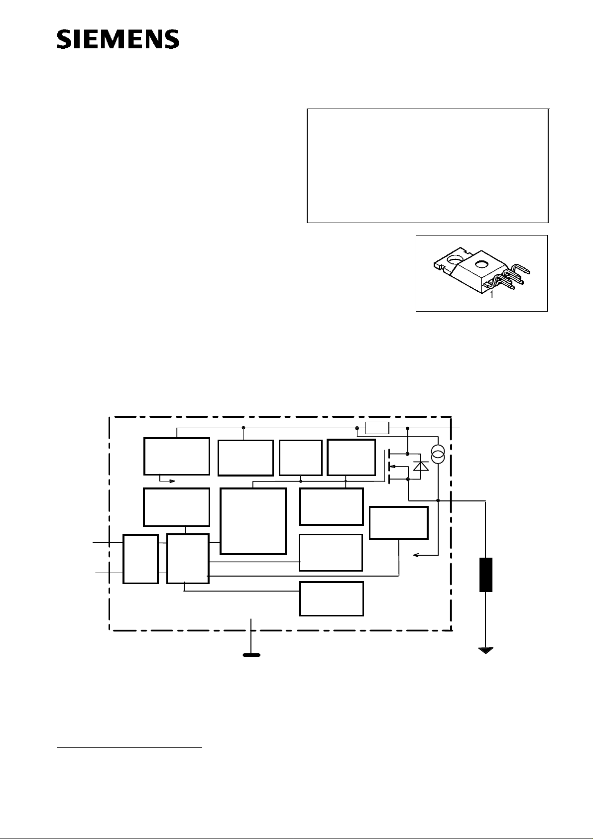
N channel vertical power FET with charge pump, ground referenced CMOS compatible input and diagnostic
feedback, integrated in Smart SIPMOS chip on chip technology. Fully protected by embedded protection
functions.
m
Ω
5
R
bb
Voltage
source
V
Logic
Voltage
sensor
IN
2
ESD
4
ST
Logic
Overvoltage
protection
Charge pump
Level shifter
Rectifier
GND
Current
limit
unclamped
Open load
detection
Short circuit
Gate
protection
Limit for
ind. loads
detection
Temperature
sensor
+ V
OUT
PROFET
bb
3
5
Load
1
Signal GND
Load GND
1)
No external components required, reverse load current limited by connected load.
2)
Additional external diode required for charged inductive loads
Semiconductor Group 1 04.96

BTS 432 I2
)
Pin Symbol Function
1 GND - Logic ground
2 IN I Input, activates the power switch in case of logical high signal
3Vbb+ Positive power supply voltage,
the tab is shorted to this pin
4 ST S Diagnostic feedback, low on failure
5 OUT
O Output to the load
(Load, L)
Maximum Ratings
at Tj = 25 °C unless otherwise specified
Parameter Symbol Values Unit
Supply voltage (overvoltage protection see page 3)
Load dump protection
R
= 2 Ω,
I
R
= 1.1 Ω,
L
V
LoadDump
t
= 200 ms, IN= low or high
d
=
U
+
V
,
A
U
s
= 13.5 V
A
Load current (Short-circuit current, see page 4)
Operating temperature range
Storage temperature range
Power dissipation (DC)
V
V
I
T
T
P
bb
)
3
s
L
j
stg
tot
self-limited A
-40 ...+150
-55 ...+150
63 V
66.5 V
°C
125 W
Inductive load switch-off energy dissipation,
single pulse
Electrostatic discharge capability (ESD
T
=150 °C:
j
E
V
AS
ESD
1.7 J
2.0 kV
(Human Body Model)
Input voltage (DC)
Current through input pin (DC)
Current through status pin (DC)
see internal circuit diagrams page 6...
V
I
I
IN
ST
IN
-0.5 ... +6 V
±5.0
mA
±5.0
Thermal resistance chip - case:
junction - ambient (free air):
R
R
thJC
thJA
SMD version, device on pcb4): ≤ tbd
3)
VS is setup without DUT connected to the generator per ISO 7637-1 and DIN 40839
)
4
Device on 50mm*50mm*1.5mm epoxy PCB FR4 with 6cm
connection. PCB is vertical without blown air.
2
(one layer, 70µm thick) copper area for V
Semiconductor Group 2
≤ 1
≤ 75
K/W
bb

BTS 432 I2
j
Electrical Characteristics
Parameter and Conditions Symbol Values Unit
at Tj = 25 °C,
Load Switching Capabilities and Characteristics
On-state resistance (pin 3 to 5)
V
= 12 V unless otherwise specified
bb
min typ max
IL = 2 A
T
=25 °C:
j
T
=150 °C:
j
Nominal load current (pin 3 to 5)
ISO Proposal:
V
ON
= 0.5 V,
T
= 85 °C
C
Output current (pin 5) while GND disconnected or
GND pulled up, VIN= 0, see diagram page 7,
T
=-40...+150°C
Turn-on time to 90%
Turn-off time to 10%
R
= 12 Ω
L
T
=-40...+150°C
,
j
V
V
OUT
OUT
Slew rate on
10 to 30%
OUT
R
,
= 12 Ω
L
T
=-40...+150°C
,
j
V
Slew rate off
70 to 40%
V
OUT
,
R
L
= 12 Ω
T
=-40...+150°C
,
j
Operating Parameters
)
Operating voltage
5
Undervoltage shutdown
Undervoltage restart
T
=-40...+150°C:
j
T
=-40...+150°C:
j
T
=-40...+150°C:
j
Undervoltage restart of charge pump
see diagram page 12
T
=-40...+150°C:
j
Undervoltage hysteresis
V
∆
bb(under)
Overvoltage shutdown
Overvoltage restart
Overvoltage hysteresis
Overvoltage protection
I
=40 mA
bb
=
V
bb(u rst)
-
V
bb(under)
)
6
T
=-40...+150°C:
j
T
=-40...+150°C:
j
T
=-40...+150°C: ∆
j
T
=-40°C:
j
T
=25...+150°C:
j
Standby current (pin 3)
=5 V
T
=-40...+25°C
j
T
=150°C:
j
VIN=0, IST=0
,
Operating current (Pin 1)7),
V
IN
:
:
:
R
I
I
t
t
dV /dt
-dV/dt
V
V
V
V
∆
V
V
V
I
I
ON
L(ISO)
L(GNDhigh)
on
off
on
off
bb(on)
bb(under)
bb(u rst)
bb(ucp)
V
bb(under)
bb(over)
bb(o rst)
V
bb(over)
bb(AZ)
bb(off)
GND
-- 30
55
38
70
mΩ
911 --A
-- -- 1 mA
50
10
160
--
300
80
µs
0.4 -- 2.5 V/µs
1--5V/µs
4.5 -- 42 V
2.4 -- 4.5 V
-- -- 4.5 V
-- 6.5 7.5 V
-- 0.2 -- V
42 -- 52 V
42 -- -- V
-- 0.2 -- V
60
63
--
67
-- V
µA
--
--
40
50
70
110
-- 1.1 -- mA
)
5
At supply voltage increase up to
6)
)
7
see also
Add
V
I
, if
ST
in table of protection functions and circuit diagram page 7. Meassured without load
ON(CL)
I
> 0, add
ST
V
= 6.5 V typ without charge pump,
bb
I
V
, if
IN
>5.5 V
IN
V
OUT
≈
V
- 2 V
bb
.
Semiconductor Group 3

BTS 432 I2
j
j
Parameter and Conditions Symbol Values Unit
at Tj = 25 °C,
Protection Functions
Initial peak short circuit current limit (pin 3 to 5)
( max 400 µs if VON > V
Repetitive short circuit current limit
T
j
Short circuit shutdown delay after input pos. slope
V
>
ON
min value valid only, if input "low" time exceeds 30 µs
Output clamp (inductive load switch off)
at V
OUT
Short circuit shutdown detection voltage
(pin 3 to 5)
Thermal overload trip temperature
Thermal hysteresis
Inductive load switch-off energy dissipation9),
T
j Start
Reverse battery (pin 3 to 1)
Integrated resistor in Vbb line
V
= 12 V unless otherwise specified
bb
ON(SC)
=
T
(see timing diagrams, page 10)
jt
V
= Vbb - V
ON(SC)
,
ON(CL)
I
= 30 mA
,
L
= 150 °C, single pulse
10
min typ max
)
8
,
I
L(SCp)
)
=-40°C:
T
=25°C:
T
=+150°C:
j
T
I
L(SCr)
--
--
22
--
42
--
72
A
--
--
20 33 -- A
T
=-40..+150°C:
j
)
V
V
bb
bb
= 12 V:
= 24 V:
t
d(SC)
V
ON(CL)
V
ON(SC)
T
jt
∆T
E
AS
E
Load12
E
Load24
-
V
bb
R
bb
80 -- 400
µ
-- 58 -- V
-- 8.3 -- V
150 -- -- °C
jt
-- 10 -- K
-- -- 1.7
1.3
1.0
-- -- 32 V
-- 120 --
Ω
s
J
Diagnostic Characteristics
Open load detection current
Open load detection voltage
)
8
Short circuit current limit for max. duration of 400 µs, prior to shutdown (see t
9)
While demagnetizing load inductance, dissipated energy in PROFET is
V
2
= 1/
E
AS
)
10
Reverse load current (through intrinsic drain-source diode) is normally limited by the connected load.
Reverse current I
these condition is dependent on the size of the heatsink. Reverse I
external GND-resistor (150 Ω). Input and Status currents have to be limited (see max. ratings page 2 and
circuit page 7).
2
*
*
L
I
L
ON(CL)
* (
V
ON(CL)
of ≈ 0.3 A at Vbb= -32 V through the logic heats up the device. Time allowed under
GND
), see diagram page 8
-
V
bb
=-40..150°C:
T
j
I
L(off)
V
OUT(OL)
can be reduced by an additional
GND
10 30 60
234V
page 4)
d(SC)
= ∫
E
AS
V
ON(CL)
*
(t) dt, approx.
i
L
A
µ
Semiconductor Group 4
BTS 432 I2
)
Parameter and Conditions Symbol Values Unit
at Tj = 25 °C,
Input and Status Feedback
Input turn-on threshold voltage
Input turn-off threshold voltage
Input threshold hysteresis
Off state input current (pin 2)
V
= 12 V unless otherwise specified
bb
)
11
T
T
=-40..+150°C:
j
=-40..+150°C:
j
V
= 0.4 V:
IN
V
IN(T+)
V
IN(T-)
∆
V
I
IN(off)
IN(T)
min typ max
1.5 -- 2.4 V
1.0 -- -- V
-- 0.5 -- V
1--30
µ
A
On state input current (pin 2)
Delay time for status with open load
after Input neg. slope (see diagram page 12)
Status invalid after positive input slope
(short circuit)
T
=-40 ... +150°C:
j
Status output (CMOS
T
=-40...+150°C,
j
T
=-40...+150°C,
j
Max. status current for
valid status output,
T
=-40...+150°C
j
I
ST
current source
current sink
V
= 3.5 V:
IN
I
= - 50 µA:
ST
= +1.6 mA:
(out):
(in) :
I
IN(on)
t
d(ST OL3)
t
d(ST SC)
V
ST(high)
V
ST(low)
-I
ST
13)
+I
ST
12
10 25 50
40 -- 300
80 200 400
)
4.4
--
--
--
5.1
--
--
--
6.5
0.4
0.25
1.6
µ
A
µ
µ
V
mA
s
s
11)
If a ground resistor R
)
12
VSt
)
13
No current sink capability during undervoltage shutdown
high
V
≈
during undervoltage shutdown
bb
is used, add the voltage drop across this resistor.
GND
Semiconductor Group 5
 Loading...