

Siemens BSS159 Datasheet
SIPMOS ® Small-Signal Transistor
• N channel
• Depletion mode
• High dynamic resistance
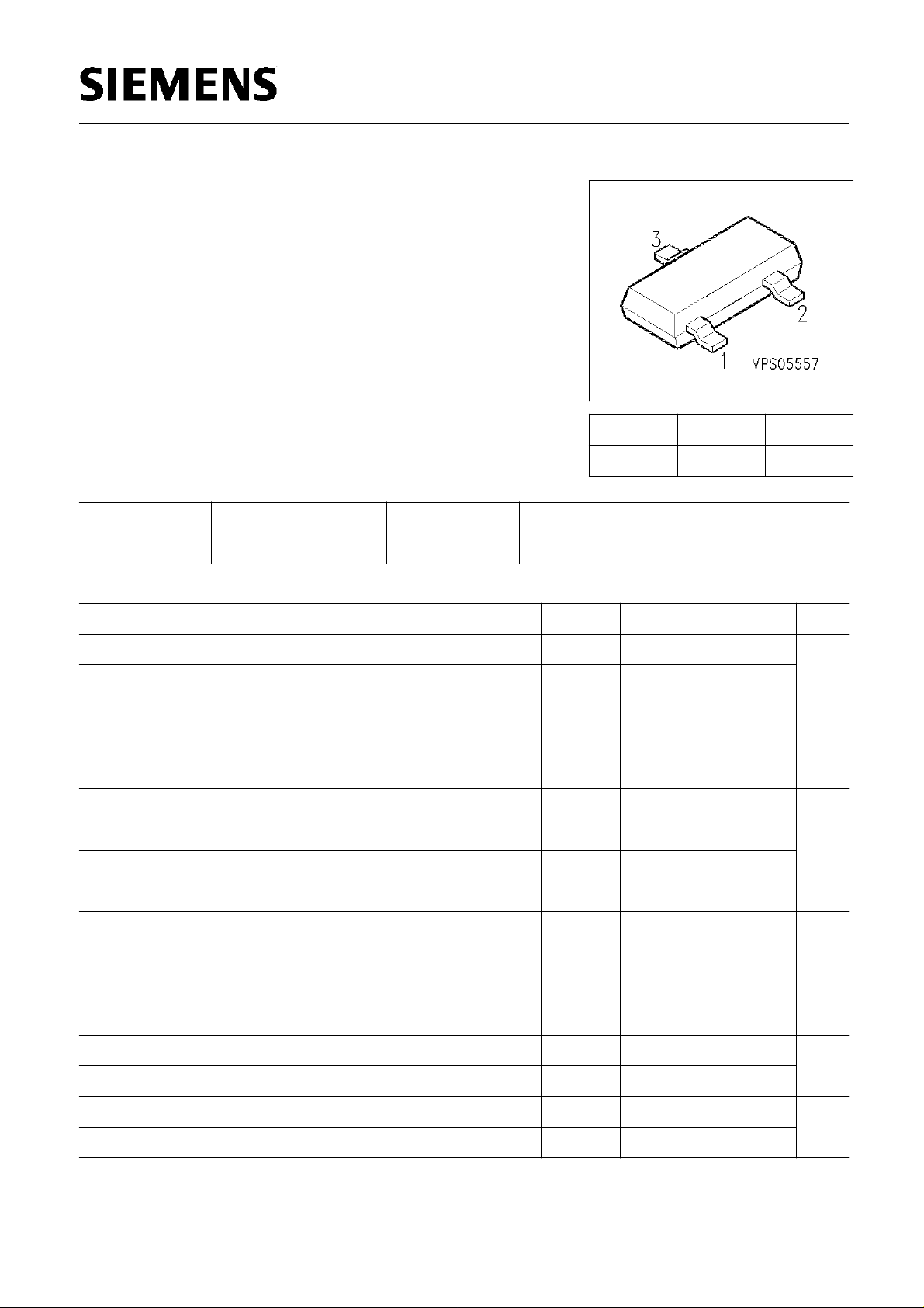
BSS 159
Preliminary data
Pin 1 Pin 2 Pin 3
G S D
Type
V
DS
I
D
R
DS(on)
Package Ordering Code
BSS 159 50 V 0.16 A 8 Ω SOT-23 Q67050-T6
Maximum Ratings
Parameter Symbol Values Unit
Drain source voltage
Drain-gate voltage
R
= 20 kΩ
GS
Gate source voltage
Gate-source peak voltage, aperiodic
Continuous drain current
T
= 25 °C
A
DC drain current, pulsed
T
= 25 °C
A
Power dissipation
T
= 25 °C
A
V
DS
V
DGR
V
GS
V
gs
I
D
I
Dpuls
P
tot
50 V
50
± 14
± 20
A
0.16
0.48
W
0.36
Chip or operating temperature
Storage temperature
Thermal resistance, chip to ambient air
Therminal resistance, chip-substrate - reverse side
1)
T
j
T
stg
R
thJA
R
thJSR
-55 ... + 150 °C
-55 ... + 150
≤ 350 K/W
≤ 285
DIN humidity category, DIN 40 040 E
IEC climatic category, DIN IEC 68-1 55 / 150 / 56
1) For package mounted on aluminium 15 mm x 16.7 mm x 0.7 mm.
Semiconductor Group 1 May-30-1996
BSS 159
Preliminary data
Electrical Characteristics, at
T
= 25°C, unless otherwise specified
j
Parameter Symbol Values Unit
min. typ. max.
Static Characteristics
Drain-source breakdown voltage
V
= -10 V,
GS
I
= 250 µA
D
Gate threshold voltage
V
= 3 V,
DS
I
= 10 µA
D
Drain-source cutoff current
V
V
DS
DS
= 50 V,
= 50 V,
V
V
GS
GS
= -10 V,
= -10 V,
T
= 25 °C
j
T
= 125 °C
j
On-state drain current
V
= 0 V,
GS
V
= 10 V
DS
V
(BR)DSV
V
GS(th)
I
DSV
I
D(on)
50 - -
-3 -2.5 -1.5
-
-
-
-
1
-
70 200 -
V
µA
mA
Gate-source leakage current
V
= 20 V,
GS
V
DS
= 0 V
Drain-Source on-resistance
V
= 0 V,
GS
I
= 0.07 A
D
I
GSS
R
DS(on)
nA
- 10 100
Ω
- 4 8
Semiconductor Group 2 May-30-1996
 Loading...