

Siemens BSS131 Datasheet
BSS 131
SIPMOS
®
Small-Signal Transistor
• N channel
• Enhancement mode
• Logic Level
• V
GS(th)
Type
BSS 131 240 V 0.1 A 16
= 0.8...2.0V
V
DS
I
D
R
DS(on)
Ω
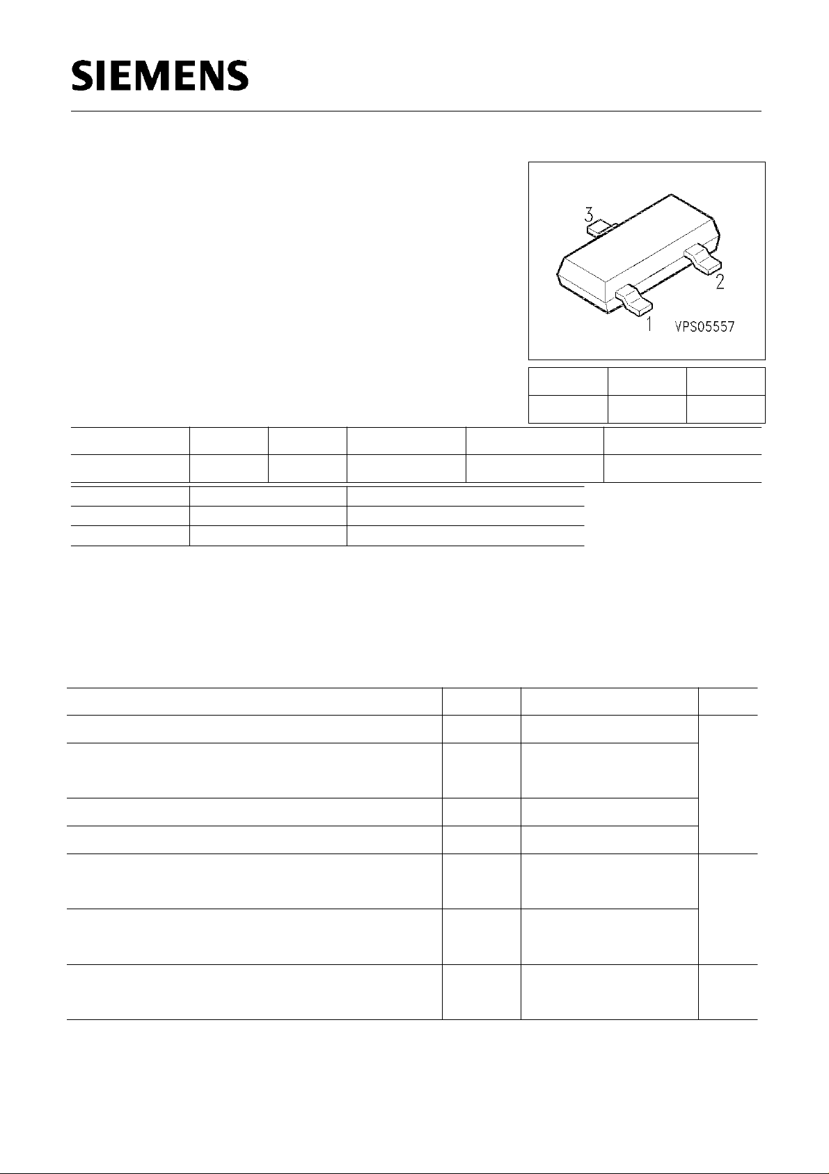
Package Marking
SOT-23 SRs
Type Ordering Code Tape and Reel Information
BSS 131 Q62702-S565 E6327
BSS 131 Q67000-S229 E6433
Pin 1 Pin 2 Pin 3
G S D
Maximum Ratings
Parameter Symbol Values Unit
Drain source voltage
Drain-gate voltage
R
= 20 k
GS
Ω
Gate source voltage
Gate-source peak voltage,aperiodic
Continuous drain current
T
= 26 °C
A
DC drain current, pulsed
T
= 25 °C
A
Power dissipation
T
= 25 °C
A
V
DS
V
DGR
V
GS
V
gs
I
D
I
Dpuls
P
tot
240 V
240
±
14
±
20
0.1
0.4
0.36
A
W
Semiconductor Group 1 Sep-13-1996
BSS 131
Maximum Ratings
Parameter Symbol Values Unit
Chip or operating temperature
Storage temperature
Thermal resistance, chip to ambient air
Therminal resistance, chip-substrate- reverse side
1)
T
j
T
stg
R
thJA
R
thJSR
-55 ... + 150 °C
-55 ... + 150
≤
350 K/W
≤
285
DIN humidity category, DIN 40 040 E
IEC climatic category, DIN IEC 68-1 55 / 150 / 56
1) For package mounted on aluminium 15 mm x 16.7 mm x 0.7 mm
Electrical Characteristics, at
T
= 25°C, unless otherwise specified
j
Parameter Symbol Values Unit
min. typ. max.
Static Characteristics
Drain- source breakdown voltage
V
= 0 V,
GS
I
= 0.25 mA,
D
T
= 25 °C
j
Gate threshold voltage
=
V
GS
V
DS, ID
= 1 mA
Zero gate voltage drain current
V
V
V
DS
DS
DS
= 240 V,
= 240 V,
= 130 V,
V
V
V
GS
GS
GS
= 0 V,
= 0 V,
= 0 V,
T
= 25 °C
j
T
= 125 °C
j
T
= 25 °C
j
Gate-source leakage current
V
= 20 V,
GS
V
DS
= 0 V
Drain-Source on-state resistance
V
V
GS
GS
= 10 V,
= 4.5 V,
I
= 0.1 A
D
I
= 0.1 A
D
V
(BR)DSS
V
GS(th)
I
DSS
I
GSS
R
DS(on)
240 - -
0.8 1.4 2
-
-
-
0.1
2
-
1 µA
60
30
- 1 10
-
-
12
15
16
26
V
nA
nA
Ω
Semiconductor Group 2 Sep-13-1996
BSS 131
Electrical Characteristics, at
T
= 25°C, unless otherwise specified
j
Parameter Symbol Values Unit
min. typ. max.
Dynamic Characteristics
Transconductance
≥
V
2
DS
I
*
D * RDS(on)max, ID
= 0.1 A
Input capacitance
V
= 0 V,
GS
V
= 25 V, f = 1 MHz
DS
Output capacitance
V
= 0 V,
GS
V
= 25 V, f = 1 MHz
DS
Reverse transfer capacitance
V
= 0 V,
GS
V
= 25 V, f = 1 MHz
DS
Turn-on delay time
V
R
DD
GS
= 30 V,
= 50
Ω
V
GS
= 10 V,
I
= 0.26 A
D
g
fs
C
iss
C
oss
C
rss
t
d(on)
S
0.06 0.14 pF
- 60 80
- 8 12
- 3.5 5
ns
- 5 8
Rise time
V
R
DD
GS
= 30 V,
= 50
Ω
V
GS
= 10 V,
Turn-off delay time
V
R
DD
GS
= 30 V,
= 50 Ω
V
GS
= 10 V,
Fall time
V
R
DD
GS
= 30 V,
= 50 Ω
V
GS
= 10 V,
I
= 0.26 A
D
I
= 0.26 A
D
I
= 0.26 A
D
t
r
t
d(off)
t
f
- 8 12
- 12 16
- 15 20
Semiconductor Group 3 Sep-13-1996
 Loading...