

Siemens BPW21 Datasheet
BPW 21
Silizium-Fotodiode für den sichtbaren Spektralbereich
Silicon Photodiode for the visible spectral range
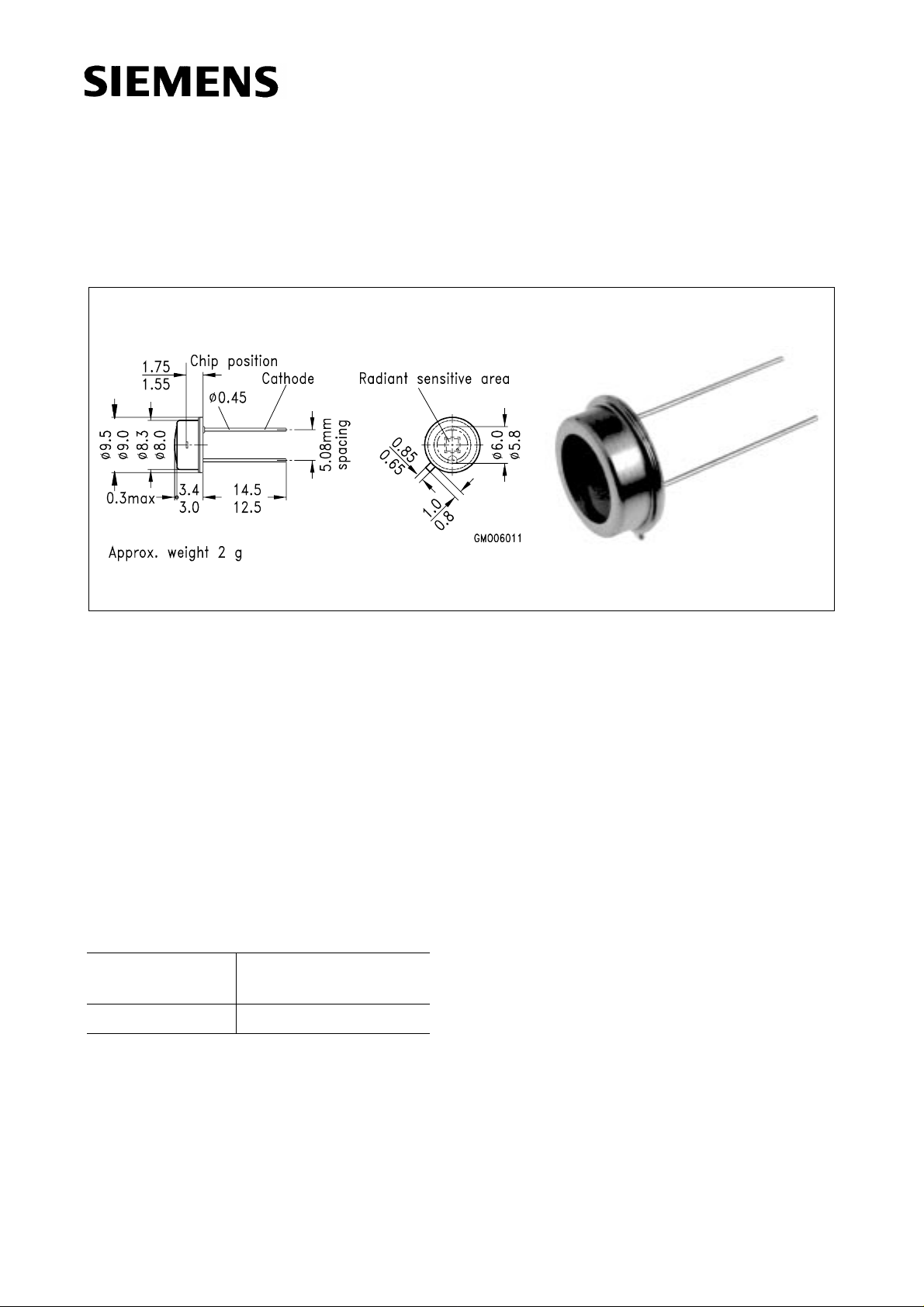
Maße in mm, wenn nicht anders angegeben/Dimensions in mm, unless otherwise specified.
BPW 21
fmo06011
Wesentliche Merkmale
● Speziell geeignet für Anwendungen im
Bereich von 350 nm bis 820 nm
● Angepaßt an die Augenempfindlichkeit (V
● Hermetisch dichte Metallbauform (ähnlich
TO-5)
Anwendungen
● Belichtungsmesser für Tageslicht
● Für Kunstlicht mit hoher Farbtemperatur in
der Fotografie und Farbanalyse
Typ
Type
Bestellnummer
Ordering Code
BPW 21 Q62702-P885
Features
● Especially suitable for applications from
350 nm to 820 nm
)
λ
● Adapted to human eye sensitivity (V
● Hermetically sealed metal package (similar
)
λ
to TO-5)
Applications
● Exposure meter for daylight
● For artificial light of high color temperature in
photographic fields and color analysis
Semiconductor Group 1 1998-11-13
Grenzwerte
Maximum Ratings
BPW 21
Bezeichnung
Description
Betriebs- und Lagertemperatur
Symbol
Symbol
T
; T
op
stg
Operating and storage temperature range
Löttemperatur (Lötstelle 2 mm vom
T
S
Gehäuse entfernt bei Lötzeit t ≤ 3 s)
Soldering temperature in 2 mm distance
from case bottom (t ≤ 3 s)
Sperrspannung
V
R
Reverse voltage
Verlustleistung, TA = 25 °C
P
tot
Total power dissipation
Kennwerte (TA = 25 °C, Normlicht A, T = 2856 K)
Characteristics (TA = 25 °C, standard light A, T = 2856 K)
Bezeichnung
Description
Symbol
Symbol
Wert
Value
Einheit
Unit
– 40 ... + 80 °C
235 °C
10 V
250 mW
Wert
Value
Einheit
Unit
Fotoempfindlichkeit, VR = 5 V
Spectral sensitivity
Wellenlänge der max. Fotoempfindlichkeit
Wavelength of max. sensitivity
Spektraler Bereich der Fotoempfindlichkeit
S = 10 % von S
max
Spectral range of sensitivity
S = 10 % of S
max
Bestrahlungsempfindliche Fläche
Radiant sensitive area
Abmessung der bestrahlungsempfindlichen
Fläche
Dimensions of radiant sensitive area
Abstand Chipoberfläche zu Gehäuseoberfläche
Distance chip front to case surface
Halbwinkel
Half angle
S
λ
S max
10 (≥ 5.5) nA/lx
550 nm
λ 350 ... 820 nm
A 7.34 mm
L × B
L
× W
H
ϕ±55 Grad
2.73 × 2.73 mm × mm
1.9 ... 2.3 mm
deg.
2
Semiconductor Group 2 1998-11-13
 Loading...