

Siemens BP104S Datasheet
Neu: Silizium-PIN-Fotodiode
New: Silicon PIN Photodiode
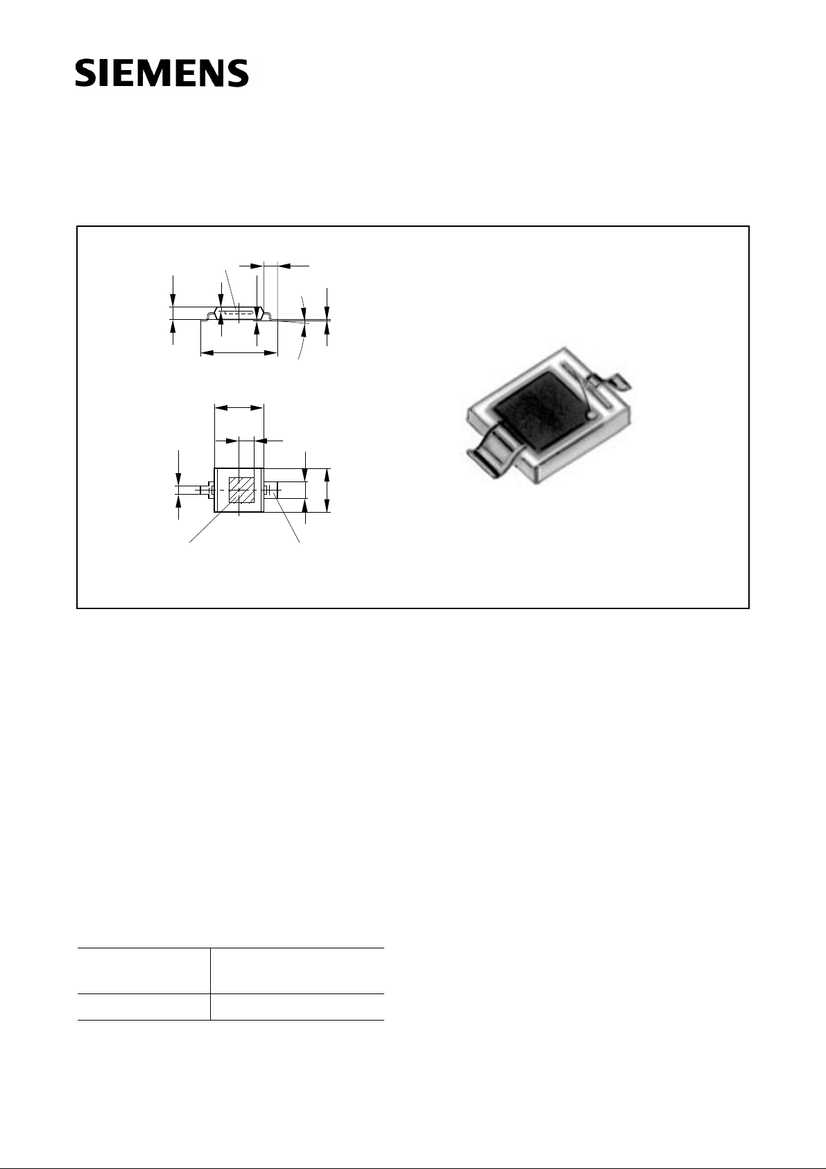
BP 104 S
0...0.1
1.1
0.9
0.2
0...5˚
1.5
1.7
4.0
GEO06861
0.1
3.7
Features
● Especially suitable for applications from
400 nm to 1100 nm
● Short switching time (typ. 20 ns)
● Suitable for vapor-phase and IR-reflow
soldering
● Suitable for SMT
Chip position
1.2
1.1
0.3
6.7
6.2
4.5
4.3
1.6
±0.2
0.9
0.7
Photosensitive area Cathode lead
2.20 mm x 2.20 mm
Maße in mm, wenn nicht anders angegeben/Dimensions in mm, unless otherwise specified.
Wesentliche Merkmale
● Speziell geeignet für Anwendungen im
Bereich von 400 nm bis 1100 nm
● Kurze Schaltzeit (typ. 20 ns)
● geeignet für Vapor-Phase Löten und IR-
Reflow-Löten
● SMT-fähig
feo06862
Anwendungen
● Lichtschranken für Gleich- und
Wechsellichtbetrieb
● IR-Fernsteuerungen
● Industrieelektronik
● “Messen/Steuern/Regeln”
Typ
Type
Bestellnummer
Ordering Code
Applications
● Photointerrupters
● IR remote controls
● Industrial electronics
● For control and drive circuits
BP 104 S Q62702-P1605
Semiconductor Group 1 1997-11-19
Grenzwerte
Maximum Ratings
BP 104 S
Bezeichnung
Description
Betriebs- und Lagertemperatur
Symbol
Symbol
T
; T
op
stg
Operating and storage temperature range
Sperrspannung
V
R
Reverse voltage
Verlustleistung, TA = 25 °C
P
tot
Total power dissipation
Kennwerte (TA = 25 °C, Normlicht A, T = 2856 K)
Characteristics (TA = 25 °C, standard light A, T = 2856 K)
Bezeichnung
Description
Fotoempfindlichkeit VR = 5 V
Symbol
Symbol
S 55 (≥ 40) nA/lx
Spectral sensitivity
Wellenlänge der max. Fotoempfindlichkeit
λ
S max
Wavelength of max. sensitivity
Wert
Value
Einheit
Unit
– 40 ... + 85 °C
20 V
150 mW
Wert
Value
Einheit
Unit
850 nm
Spektraler Bereich der Fotoempfindlichkeit
S = 10 % von S
max
Spectral range of sensitivity
S = 10 % of S
max
Bestrahlungsempfindliche Fläche
Radiant sensitive area
Abmessung der bestrahlungsempfindlichen
Fläche
Dimensions of radiant sensitive area
Abstand Chipoberfläche zu Gehäuseoberfläche
Distance chip front to case surface
Halbwinkel
Half angle
Dunkelstrom, VR = 10 V
Dark current
Spektrale Fotoempfindlichkeit, λ = 850 nm
Spectral sensitivity
Quantenausbeute, λ = 850 nm
Quantum yield
λ 400 ... 1100 nm
A 4.84 mm
L × B
L
× W
H
2.20 × 2.20 mm × mm
0.3 mm
2
ϕ±60 Grad
deg.
I
R
S
λ
2 (≤ 30) nA
0.62 A/W
η 0.90 Electrons
Photon
Semiconductor Group 2 1997-11-19
 Loading...