

BP 103 B
BP 103 BF
.
NPN-Silizium-Fototransistor
NEU: NPN-Silizium-Fototransistor mit Tageslichtsperrfilter
BP 103 B
BP 103 BF
Silicon NPN Phototransistor
NEW: Silicon NPN Phototransistor with Daylight Filter
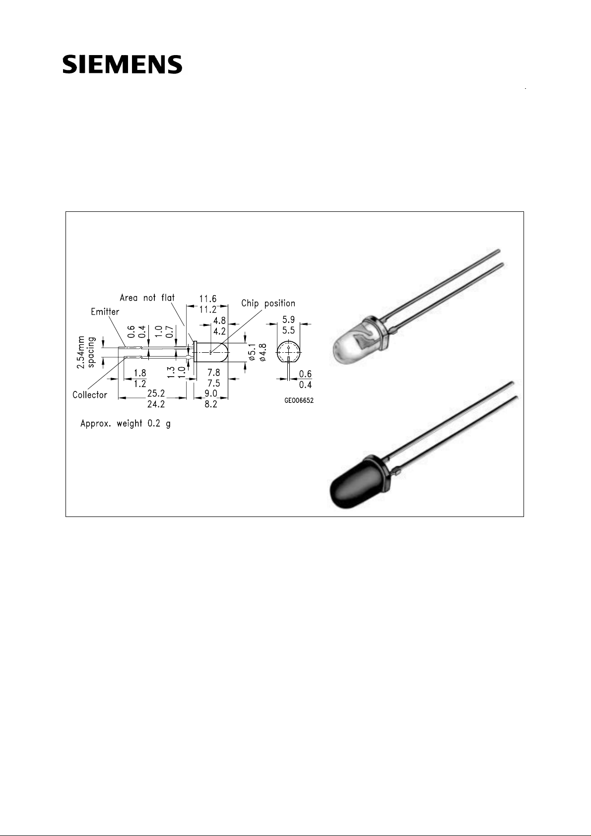
Maβe in mm, wenn nicht anders angegeben/Dimensions in mm, unless otherwise specified.
Wesentliche Merkmale
● Speziell geeignet für Anwendungen im
Bereich von 420 nm bis 1130 nm (BP 103 B)
und bei 880 nm (BP 103 BF)
● Hohe Linearität
● 5 mm-Plastikbauform im LED-Gehäuse
● Gruppiert lieferbar
Anwendungen
● Computer-Blitzlichtgeräte
● Lichtschranken für Gleich- und
Wechsellichtbetrieb
● Industrieelektronik
● “Messen/Steuern/Regeln”
Features
● Especially suitable for applications from
420 nm to 1130 nm (BP 103 B) and of
880 nm (BP 103 BF)
● High linearity
● 5 mm LED plastic package
● Available in groups
Applications
● Computer-controlled flashes
● Light-reflecting switches for steady and
varying intensity
● Industrial electronics
● For control and drive circuits
Semiconductor Group 204

BP 103 B
BP 103 BF
Typ (*ab 4/95)
Type (*as of 4/95)
BP 103 B-2
(*SFH 300-2)
BP 103 B-3
(*SFH 300-3)
BP 103 B-4
1)
(*SFH 300-4)
BP 103 BF-2
Bestellnummer
Ordering Code
Gehäuse
Package
Q62702-P85-S2 T1
spieβe im 2.54-mm-Raster (
Q62702-P85-S3
chung: kürzerer Lötspieβ, flach am Gehäuseboden
T13/4, transparent and black epoxy resin lens, sol-
Q62702-P85-S4
der tabs 2.54 mm (
marking: short solder lead, flat at package bottom
Q62702-P1192
3
/4, klares bzw. schwarzes Epoxy-Gieβharz, Löt-
1
/10”) lead spacing, collector
1
/10”), Kollektorkennzei-
(*SFH 300 FA-2)
BP 103 BF-3
Q62702-P1057
(*SFH 300 FA-3)
BP 103 BF-4
Q62702-P1058
(*SFH 300 FA-4)
1)
Lieferung in dieser Gruppe kann wegen Ausbeuteschwankungen nicht immer sichergestellt werden.
Wir behalten uns in diesem Fall die Lieferung einer Ersatzgruppe vor.
1)
Supplies out of this group cannot always be guaranteed due to unforseeable spread of yield.
In this case we will reserve us the right of delivering a substitute group.
Grenzwerte
Maximum Ratings
Bezeichnung
Description
Betriebs- und Lagertemperatur
Operating and storage temperature range
Löttemperatur bei Tauchlötung
Lötstelle ≥ 2 mm vom Gehäuse,
Lötzeit t ≤ 5s
Dip soldering temperature ≥ 2 mm distance
from case bottom, soldering time t ≤ 5s
Löttemperatur bei Kolbenlötung
Lötstelle ≥ 2 mm vom Gehäuse,
Lötzeit t ≤ 3s
Iron soldering temperature ≥ 2 mm distance
from case bottom t ≤ 3s
Kollektor-Emitterspannung
Collector-emitter voltage
Kollektorstrom
Collector current
Symbol
Symbol
T
; T
op
stg
T
S
T
S
V
CE
I
C
Wert
Value
–55 ... +100
260
300
Einheit
Unit
o
C
o
C
o
C
35 V
50 mA
Semiconductor Group 205

BP 103 B
BP 103 BF
Bezeichnung
Description
Kollektorspitzenstrom, τ < 10 µs
Collector surge current
Emitter-Kollektorspannung
Emitter-collector voltage
Verlustleistung, T
= 25oC
A
Total power dissipation
Wärmewiderstand
Thermal resistance
Kennwerte (T
= 25oC, λ = 950 nm)
A
Characteristics
Bezeichnung
Description
Wellenlänge der max. Fotoempfindlichkeit
Wavelength of max. sensitivity
Symbol
Symbol
I
CS
V
EC
P
tot
R
thJA
Symbol
Symbol
λ
S max
Wert
Value
Einheit
Unit
100 mA
7V
200 mW
375 K/W
Wert
Value
Einheit
Unit
BP 103 B BP 103 BF
850 900 nm
Spektraler Bereich der Fotoempfindlichkeit
S = 10% von S
max
Spectral range of sensitivity
S = 10% of S
max
Bestrahlungsempfindliche Fläche
Radiant sensitive area
Abmessung der Chipfläche
Dimensions of chip area
Abstand Chipoberfläche zu Gehäuseoberfläche
Distance chip front to case surface
Halbwinkel
Half angle
Kapazität, V
= 0 V, f = 1 MHz, E = 0
EC
Capacitance
Dunkelstrom
Dark current
= 35 V, E = 0
V
CEO
λ 420 ... 1130 730 ... 1120 nm
A 0.12 0.045 mm
L x B
0.5 x 0.5 0.45 x 0.45 mm x mm
L x W
H 4.1 ... 4.7 2.4 ... 2.8 mm
ϕ±25 ± 12 Grad
deg.
C
I
CEO
CE
6.5 5.0 pF
5 (≤100) 1 (≤200) nA
2
Semiconductor Group 206

BP 103 B
BP 103 BF
Die Fototransistoren werden nach ihrer Fotoempfindlichkeit gruppiert und mit arabischen
Ziffern gekennzeichnet.
The phototransistors are grouped according to their spectral sensitivity and distinguished
by arabian figures.
Bezeichnung
Description
Fotostrom, λ = 950 nm
Photocurrent
E
= 0.5 mW/cm2, VCE = 5 V
e
= 1000 Ix, Normlicht/standard light A,
E
v
V
= 5 V
CE
Anstiegszeit/Abfallzeit
Rise and fall time
= 1 mA, VCC = 5 V, RL = 1 kΩ
I
C
Kollektor-Emitter-Sättigungsspannung
Collector-emitter saturation voltage
I
= I
C
PCEmin
E
= 0.5 mW/cm
e
1)
I
PCEmin
1)
I
PCEmin
1)
x 0.3,
2
ist der minimale Fotostrom der jeweiligen Gruppe
is the min. photocurrent of the specified group
Symbol
Symbol
I
PCE
I
PCE
t
, t
r
f
V
CEsat
Wert
Value
Einheit
Unit
-2 -3 -4
0.63 ... 1.25
3.4
1 ... 2
5.4
≥1.6
8.6
mA
mA
7.5 10 10 µs
130 140 150 mV
Semiconductor Group 207

BP 103 B
BP 103 BF
Relative spectral sensitivity , BP 103 B
S
= f (λ)
rel
Photocurrent I
V
= 5 V
CE
PCE/IPCE25
o
= f (TA),
Relative spectral sensitivity , BP 103 BF
S
= f (λ)
rel
Photocurrent I
= f (Ee), VCE= 5 V
PCE
Dark curent
I
CEO/ICEO25
Dark curent
I
= f (VCE), E = 0
CEO
o
= f (TA), VCE = 25 V, E = 0
Directional characteristics S
rel
= f (ϕ)
Semiconductor Group 208
Collector-emitter capacitance
C
= f (VCE), f = 1 MHz, E = 0
CE
 Loading...