

Siemens BAR81W Datasheet
BAR 81W
Semiconductor Group
Sep-04-19981
Silicon RF Switching Diode
Preliminary data
• Design for use in shunt configuration
• High shunt signal isolation
• Low shunt insertion loss
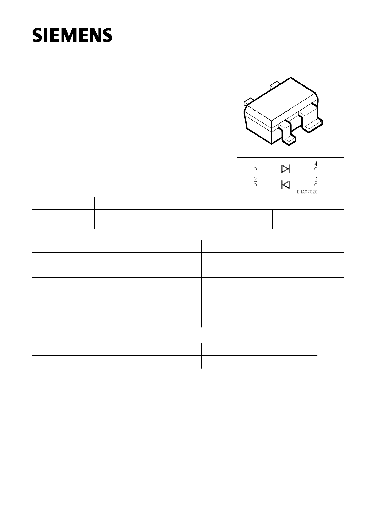
VPS05605
4
2
1
3
Type Marking Ordering Code PackagePin Configuration
Q62702-A1270 4 = C13 = A2BAR 81W 1 = A1 2 = C2 SOT-343BBs
Maximum Ratings
Symbol Value UnitParameter
Diode reverse voltage
V
R
V30
I
F
100 mAForward current
mW100
Total power dissipation,
T
S
= 138 °C
P
tot
Junction temperature
T
j
°C150
Operating temperature range -55 ...+125 °C
T
op
T
st
g
Storage temperature -55 ...+150
Thermal Resistance
Junction - ambient
1)
≤ 200
R
thJA
K/W
≤ 120
Junction - soldering point
R
thJS
1) Package mounted on alumina 15mm x 16.7mm x 0.7mm
Semiconductor Group 1 1998-11-01
BAR 81W
Semiconductor Group
Sep-04-19982
Electrical Characteristics at
T
A
= 25 °C, unless otherwise specified.
Parameter ValuesSymbol Unit
typ. max.min.
Characteristics
- - nA
I
R
Reverse current
V
R
= 20 V
20
0.93
V
F
1 VForward voltage
I
F
= 100 mA
-
AC characteristics
Diode capacitance
V
R
= 1 V, f = 1 MHz
V
R
= 3 V, f = 1 MHz
C
T
-
-
0.6
0.57
-
-
pF
Forward resistance
I
F
= 5 mA, f = 100 MHz
r
f
- 0.7 -
Ω
0.15 - nHSeries inductance
L
s
-
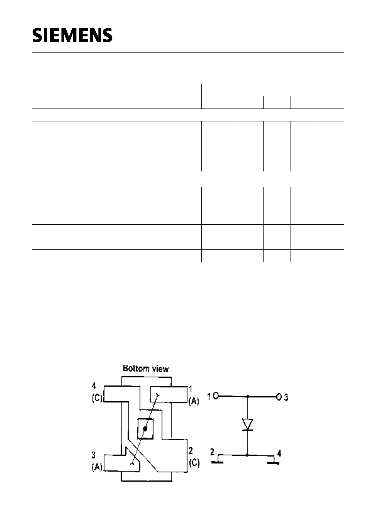
Configuration of the shunt-diode
- A perfect ground is essential for optimum isolation
- The anode pins should be used as passage for R
F
Semiconductor Group 2 1998-11-01
 Loading...