

Page 1
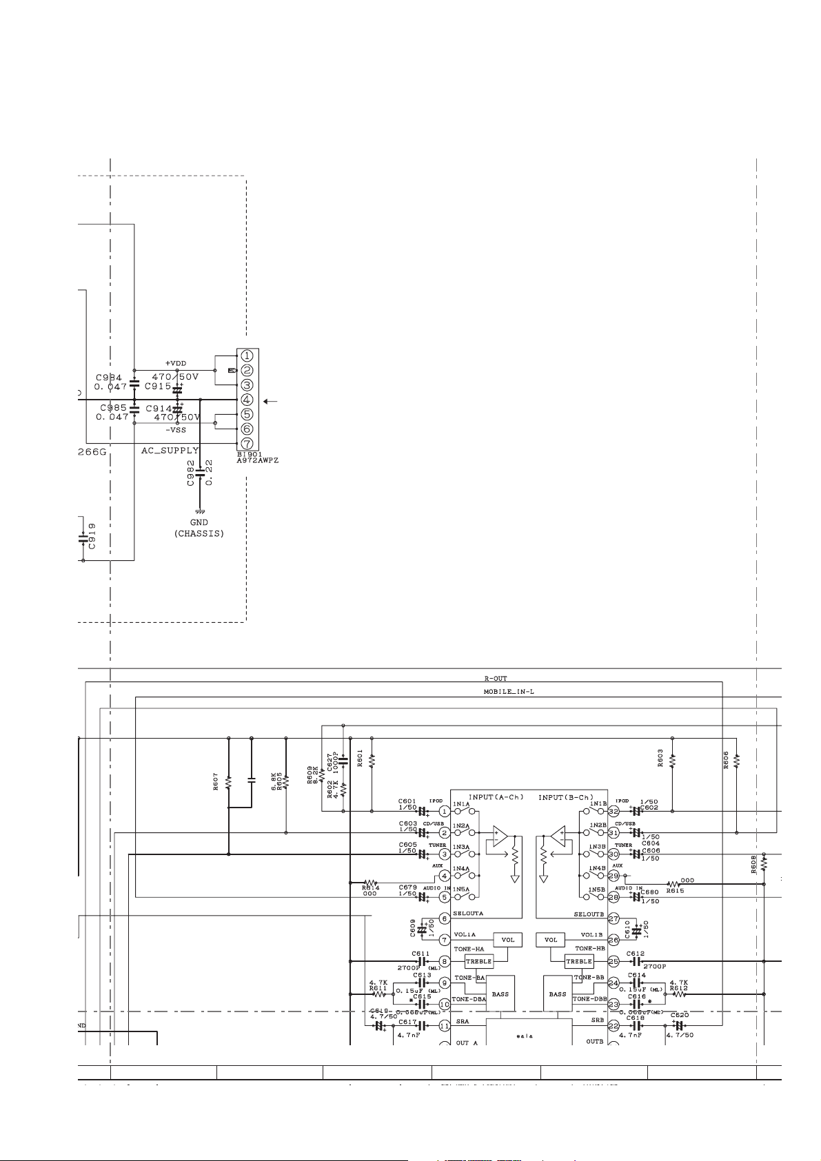
XL-DK257N
SERVICE MANUAL
No. S2807XLDK257N
MICRO COMPONENT SYSTEM
O
I
D
U
A
IN
MODEL
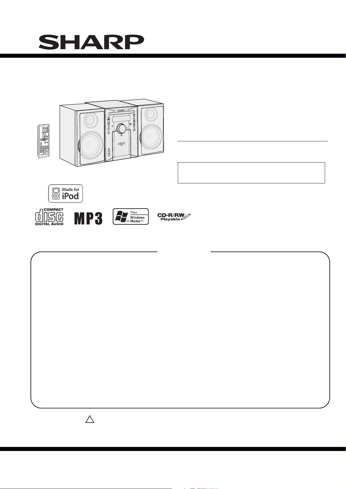
XL-DK257N Micro Component System consisting of
XL-DK257N (main unit) and CP-DK257N (speaker system).
• In the interests of user-safety (Required by safety regulations in
some countries) the set should be restored to its original condition
and only parts identical to those specified be used.
XL-DK257N
iPod is a registered trademark of Apple Inc.
CONTENTS
PRECAUTIONS FOR USING LEAD-FREE SOLDER
CHAPTER 1. GENERAL DESCRIPTION
[1] Important Service Safety Precaution ................ 1-1
[2] Important Service Notes (for U.S.A only).......... 1-1
[3] Specifications..................................................... 1-2
[4] Name Of Parts ................................................... 1-3
CHAPTER 2. ADJUSTMENTS
[1] CD Section .................................................. 2-1
[2] Test Mode .................................................... 2-2
[3] Standard Specification Of Stereo System
Error Message Display Contents ................. 2-4
CHAPTER 3. MECHANICAL DESCRIPTION
[1] Disassembly ................................................ 3-1
CHAPTER 4. BLOCK DIAGRAM
[1] Block Diagram ............................................. 4-1
CHAPTER 5. CIRCUIT DESCRIPTION
[1] Waveforms Of Servo Circuit ........................ 5-1
[2] IC Voltage .................................................... 5-3
CHAPTER 6. CIRCUIT SCHEMATICS AND PARTS
LAYOUT
[1] Notes On Schematic Diagram ..................... 6-1
[2] Types Of Transistor And LED ...................... 6-1
[3] Schematic Diagram ..................................... 6-2
[4] Charts Of Connecting Wires ...................... 6-10
[5] Wiring Side of PWB ................................... 6-12
CHAPTER 7. FLOWCHART
[1] Troubleshooting ........................................... 7-1
CHAPTER 8. OTHER
[1] Function Table Of IC .................................... 8-1
[2] FL Display.................................................... 8-9
PARTS GUIDE
Parts marked with " " are important for maintaining the safety of the set. Be sure to replace these parts with
specified ones for maintaining the safety and performance of the set.
!
SHARP CORPORATION
– 1
This document has been published to be used for
after sales service only.
The contents are subject to change without notice.
Page 2
XL-DK257N
PRECAUTIONS FOR USING LEAD-FREE SOLDER
1. Employing lead-free solder
"MAIN, POWER, AMPLIFIER, HEADPHONE, MICOM REFLASH, DISPLAY, SPEAKER, VOLUME LED LIGHT UP,
iPOD, CD PWB" of this model employs lead-free solder.
The LF symbol indicates lead-free solder, and is attached on the PWB and service manuals. The alphabetical
character following LF shows the type of lead-free solder.
Example:
Indicates lead-free solder of tin, silver and copper.
2. Using lead-free wire solder
When fixing the PWB soldered with the lead-free solder, apply lead-free wire solder. Repairing with
conventional lead wire solder may cause damage or accident due to cracks.
As the melting point of lead-free solder (Sn-Ag-Cu) is higher than the lead wire solder by 40 C, were
commend you to use a dedicated soldring bit, if you are not familiar with how to obtain lead-free wire solder or
soldering bit, contact our service station or service branch in your area.
3. Soldering
As the melting point of lead-free solder (Sn-Ag-Cu) is about 220 C which is higher than the conventional lead
solder by 40 C, and as it has poor solder wet ability, you may be apt to keep the soldering bit in contact with the
PWB for extended period of time. However, since the land may be peeled off or the maximum heat-resistance
temperature of parts may be exceeded, remove the bit from the PWB as soon as you confirm the steady
soldering condition.
Lead-free solder contains more tin, and the end of the soldering bit may be easily corrected. Make sure to turn on
and off the power of the bit as required.
If a different type of solder stays on the tip of the soldering bit, it is alloyed with lead-free solder. Clean the bit
after every use of it.
When the tip of the soldering bit is blackened during use, file it with steel wool or fine sandpaper.
Be careful when replacing parts with polarity indication on the PWB silk.
Lead-free wire solder for servicing
Ref No.
PWB-A
PWB-B
PWB-C
PWB-D 92LPWB7119CDUS
Parts No.
92LPWB7119MANS
92LPWB7119DPLS
92LPWB7119PODS
MAIN (A1), POWER (A2), AMPLIFIER (A3) , HEADPHONE (A4), MICOM REFLASH (A5)
DISPLAY (B1), SPEAKER (B2), VOLUME LED LIGHT UP (B3)
iPOD
CD
Description
– 2
i
Page 3
XL-DK257N
CHAPTER 1.
GENERAL DESCRIPTION
[1] Important Service Safety Precaution
CAUTION : “These servicing instructions are for use by qualified service personnel only. To reduce
the risk of electric shock do not perform any servicing other than that contained in the operating
instructions unless you are qualified to do so”.
WARNING
1. For continued safety, no modification of any circuit should be attempted.
2. Disconnect AC power before servicing.
CAUTION: FOR CONTINUED
PROTECTION AGAINST FIRE
HAZARD, REPLACE ONLY WITH
SAME TYPE F801, F802, 6A, 125V/
F803, F804 2A, 125V/
F805 1.6A, 125V/
F806 5A, 125V FUSES.
ATTENTION: POUR ASSURER
UNE LONGUE PROTECTION CONTRE
UN INCENDIE, REMPLACER SEULEMENT
PAR UN FUSIBLE DE
TYPE F801, F802, 6A, 125V/
F803, F804 2A, 125V/
F805 1.6A, 125V/
F806 5A, 125V FUSES.
[2] Important Service Notes (for U.S.A only)
BEFORE RETURNING THE AUDIO PRODUCT
(Fire & Shock Hazard)
Before returning the audio product to the user, perform
the following safety checks.
1. Inspect all lead dress to make certain that leads are not
pinched or that hardware is not lodged between the
chassis and other metal parts in the audio product.
2. Inspect all protective devices such as insulating
materials, cabinet, terminal board, adjustment and
compartment covers or shields, mechanical insulators
etc.
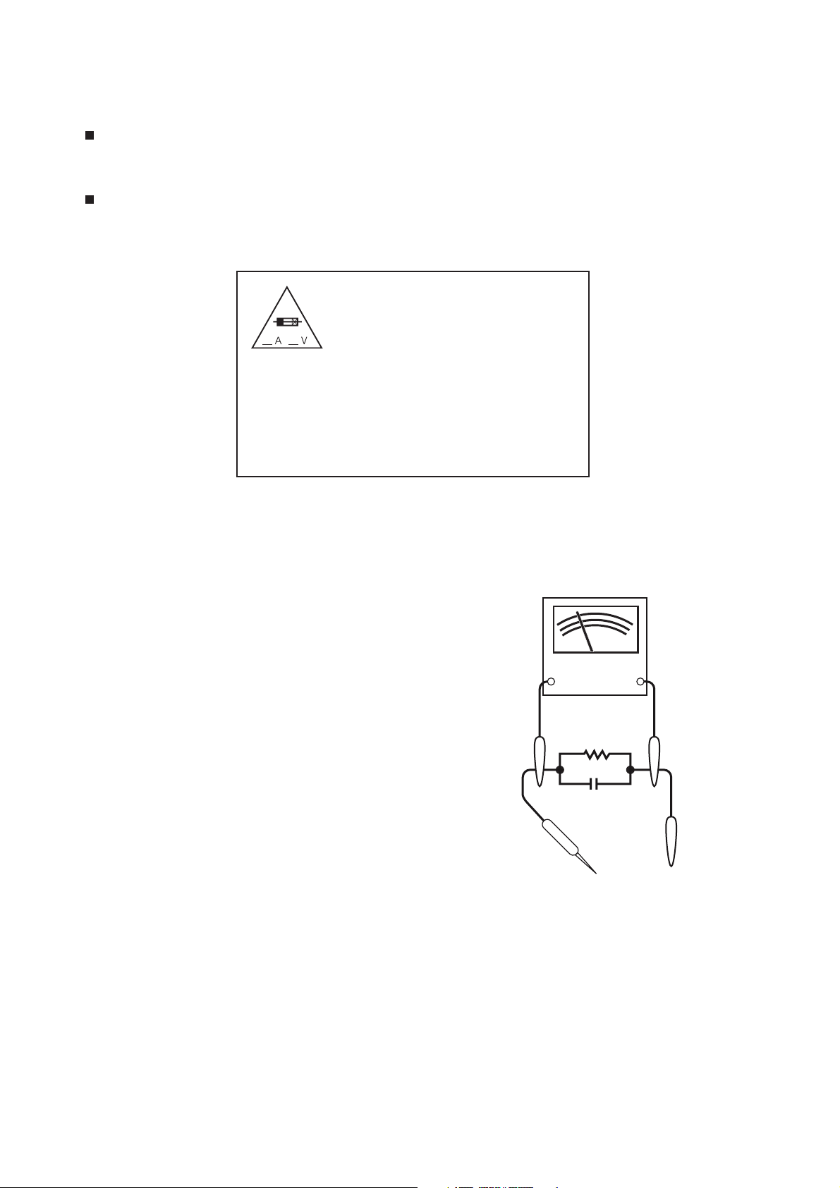
3. To be sure that no shock hazard exists, check for
leakage current in the following manner.
Plug the AC line cord directly into a 120 volt AC outlet.
*
* Using two clip leads, connect a 1.5k ohm, 10 watt
resistor paralleled by a 0.15µF capacitor in series
with all exposed metal cabinet parts and a known
earth ground, such as conduit or electrical ground
connected to earth ground.
Use a VTVM or VOM with 1000 ohm per volt, or
*
higher, sensitivity to measure the AC voltage drop
across the resistor (See diagram).
* Connect the resistor connection to all exposed metal
parts having a return path to the chassis (antenna,
metal cabinet, screw heads, knobs and control shafts,
escutcheon, etc.) and measure the AC voltage drop
across the resistor.
VTVM
AC SCALE
1.5k ohms
10W
0.15µF
TEST PROBE
TO EXPOSED
METAL PARTS
CONNECT TO
KNOWN EARTH
GROUND
All check must be repeated with the AC line cord plug
connection reversed.
Any reading of 0.3 volt RMS (this corresponds to 0.2
milliamp. AC.) Or more is excessive and indicates a
potential shock hazard which must be corrected before
returning the audio product to the owner.
1 – 1
1 – 3
Page 4
XL-DK257N
[3] Specifications
General
Power source AC 120 V ~ 60 Hz
Power consumption 56 W
Dimensions Width: 7-1/16" (180 mm)
Weight 9.5 lbs (4.3 kg)
Height: 10-2/8" (260 mm)
Depth: 10-6/8" (273 mm)
Amplifier
Output power
Output terminals Speakers: 4 ohms
Input terminals Audio In (Audio signal):
RMS : Total 160 Watts (80 Watts per
channel into 4 ohms at 1 kHz, 10%
total harmonic distortion.)
FTC : 60 Watts minimum RMS per
channel into 4 ohms from 100 Hz to
20 kHz, 10% total harmonic
distortion.
Headphones: 16 - 50 ohms
(recommended: 32 ohms)
Subwoofer pre-out (audio signal):
150 mV/10 k ohms at 70 Hz
250 mV/47 k ohms
CD player
Type Single disc multi-play compact disc player
Signal readout Non-contact, 3-beam semiconductor laser
D/A converter Multi bit D/A converter
Frequency response 20 - 20,000 Hz
Dynamic range 90 dB (1 kHz)
pickup
Tuner
Frequency range
FM: 87.5 - 108 MHz
AM: 530 - 1,720 kHz
Speaker
Type
Maximum input
power
Rated input power 80 W
Impedance 4 ohms
Dimensions Width: 5-13/16" (148 mm)
Weight 5.40 lbs (2.45 kg)/each
2-way type speaker system
2" (5 cm) tweeter
4-3/4" (12 cm) woofer
160 W
Height: 10-1/4" (260 mm)
Depth: 7-13/16" (198.5 mm)
1 – 4
1 – 2
Page 5
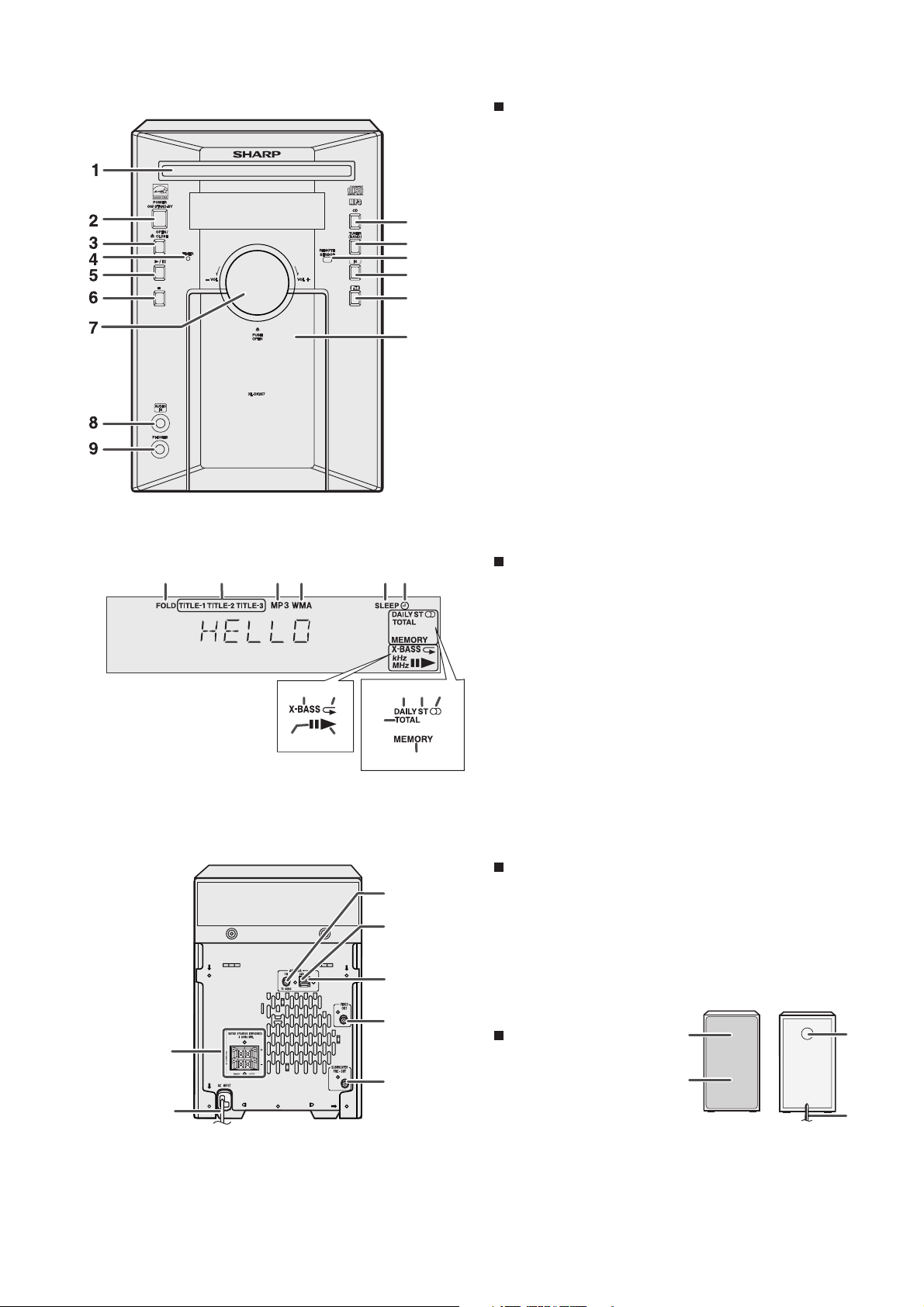
[4] Names Of Parts
4
1
2
3
Docking Station
MICRO COMPONENT SYSTEM
10
11
12
13
14
15
XL-DK257N
Front panel
1. Disc Tray
2. Power On/Stand-by Button
3. Disc Tray Open/Close Button
4. Timer Indicator
5. Disc or iPod Play or Pause button
6. Disc Stop Button
7. Volume Control
8. Audio In Jack
9. Phones Jack
10. CD Button
11. Tuner (Band) Button
12. Remote sensor
13. Audio In Button
14. iPod Button
15. iPod Docking Station
1234 56
12 13
8910
7
14
15
11
3
4
5
Display
1. MP3/WMA Folder Indicator
2. MP3/WMA Title Indicators
3. MP3 Indicator
4. WMA Indicator
5. Sleep Indicator
6. Timer Play Indicator
7. MP3/WMA Total Indicator
8. Daily Timer Indicator
9. FM Stereo Mode Indicator
10. FM Stereo Receiving Indicator
11. Memory Indicator
12. Extra Bass Indicator
13. Disc Repeat Play Indicator
14. Disc Pause Indicator
15. Disc Play Indicator
Rear panel
1. Speaker Terminals
2. AC Power Cord
3. FM 75 Ohms Antenna Jack
4. AM Antenna Ground Terminal
5. AM Loop Antenna Terminal
6. Video Out Jack
7. Subwoofer Pre-output Jack
6
Speaker system
1
7
1. Tweeter
2. Woofer
3. Bass Reflex Duct
4. Speaker Wire
2
1 – 5
1 – 3
Page 6
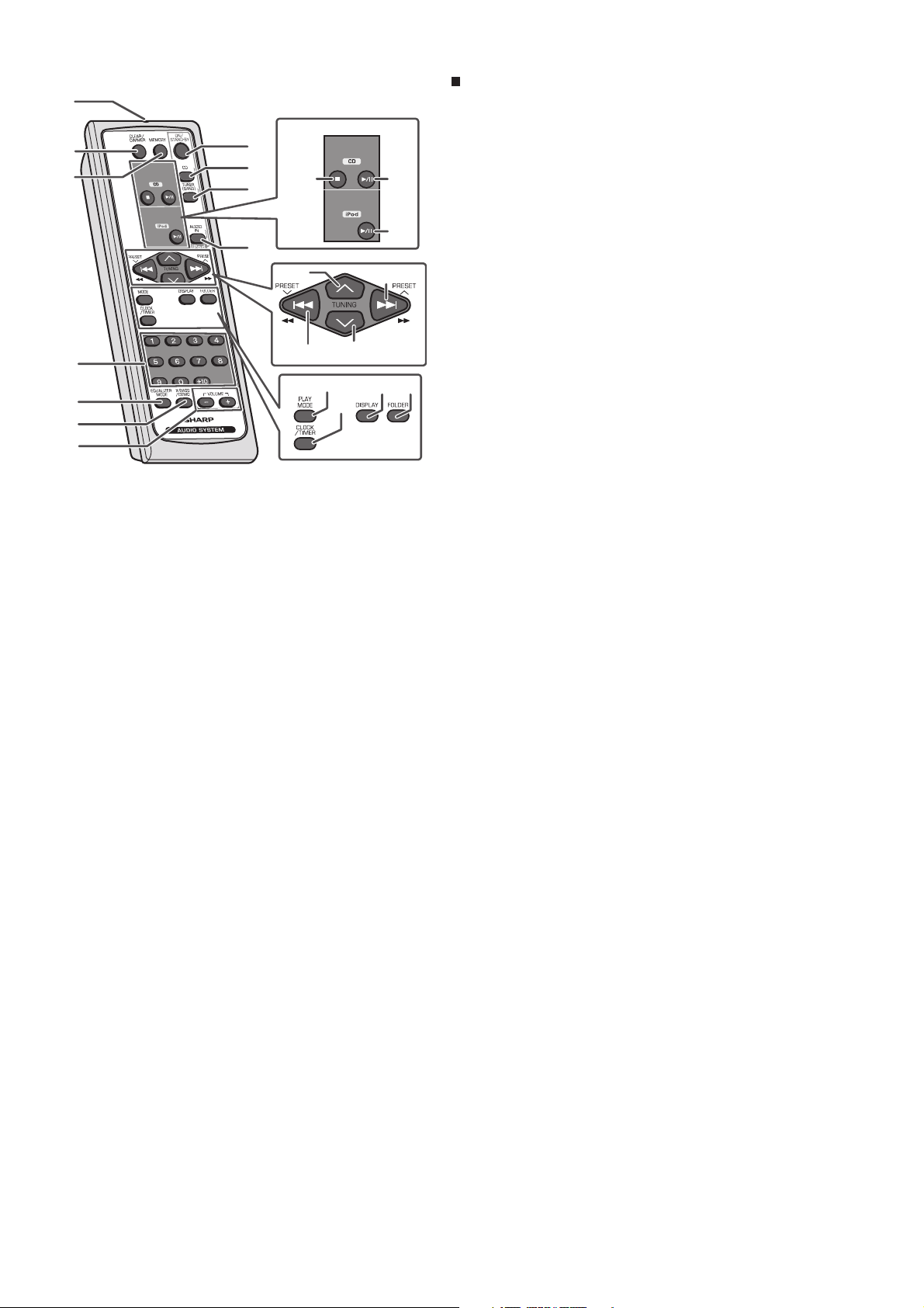
XL-DK257N
1
2
3
4
5
6
7
8
9
12
10
11
15 16
19
22
1817
13
14
20 21
Remote control
1. Remote Control Transmitter
2. Disc Clear/Dimmer, iPod Menu Button
3. Memory, iPod Enter Button
4. Disc Direct Search Buttons
5. Equalizer Mode Select Button
6. Extra Bass/Demo Button
7. Volume Up and Down Buttons
8. Power On/Stand-by Button
9. CD Button
10. Tuner (Band) Button
11. Audio In/iPod Button
12. Disc Stop Button
13. Disc Play or Pause Button
14. iPod Play or Pause Button
15. Tuning Up, Select iPod Menu Items Button
16. CD Track Up or Fast Forward, Tuner Preset Up,
Time Up Button
17. CD Track Down or Fast Reverse, Tuner Preset Down,
Time Down Button
18. Tuning Down, Select iPod Menu Items Button
19. Play Mode Button
20. Display Button
21. Folder Button
22. Clock/Timer Button
1 – 6
1 – 4
Page 7

CHAPTER 2. ADJUSTMENTS
[1] CD Section
1. CD SECTION
• Adjustment
Since this CD system incorporates the following
automatic adjustment functions, readjustment is not
needed when replacing the pickup. Therefore,
different PWBs and pickups can be combined freely.
Each time a disc is changed, these adjustments are
performed automatically. Therefore, playback of
each disc can be performed under optimum
conditions.
Items adjusted automatically
1) Offset adjustment (The offset voltage between the
head amplifier output and the VREF reference
voltage is compensated inside the IC.)
* Focus offset adjustment
* Tracking offset adjustment
2) Tracking balance adjustment
3) Gain adjustment (The gain is compensated inside
the IC so that the loop gain at the gain crossover
frequency will be 0 dB.)
XL-DK257N
* Focus gain adjustment
* Tracking gain adjustment
2 – 1
Page 8
XL-DK257N
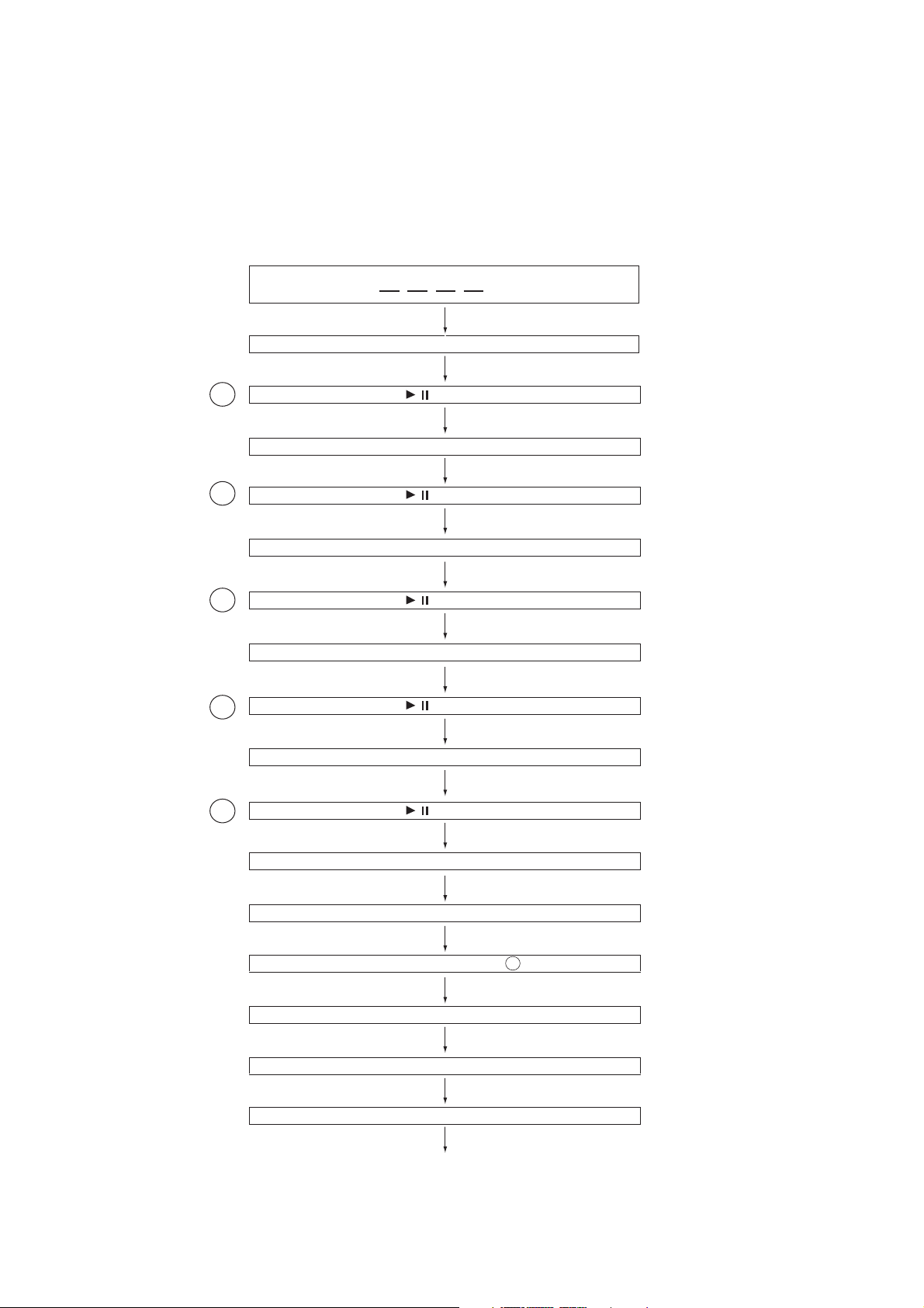
[2] Test Mode
• Setting the test mode
During AC unplug, plug-in AC while pressing down the
POWER button and CD button. Then, press the CD
button to enter the test mode.
Step
Step
Step
Step
C DTEST
OPEN/CLOSE operation is using manual. IL isn’t done
/
1
2
3
4
<< >> key input.
Laser ON.
/
<< >> key input.
Focus ON
/
<< >> key input.
CLV Servo ON
/
<< >> key input.
IL isn’t done
Step
Tracking Servo ON
/
5
Hold down << CD >> key for more than 2 sec.
Start Auto Adjustment at current pick-up location.
<< >> key input.
Reading Sub-code and Display
<<STOP>> key input.
STOP and return to Step
<<STOP>> key input.
1
2 – 2
Page 9
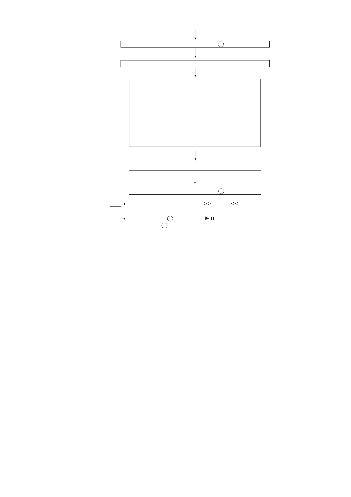
XL-DK257N
STOP and return to Step
Everytime << DISPLAY >> key input
a) Focus Balance = FB : XX
b) Focus Gain = FG : XX
c) Tracking Balance = TB : XX
d) Tracking Gain = TG : XX
e) Focus Offset = FOFF : XX
f) Tracking Offset = TOFF : XX
g) RFRP = RFRP : XX
h) Focus Error
(RW Judgement) = RW : XX - XXXX
i) Focus Error
(Other than RW Judgement) = DA : XX - XXXX
<<STOP>> key input.
STOP and return to Step
Note
Sliding the PICKUP with << >>, << >> button can be set
1
1
in STOP mode or play mode.
During at Step , if press << >> for more than 1 sec, it directly
goes to step .
1
5
/
To cancel: Power OFF
2 – 3
Page 10
XL-DK257N
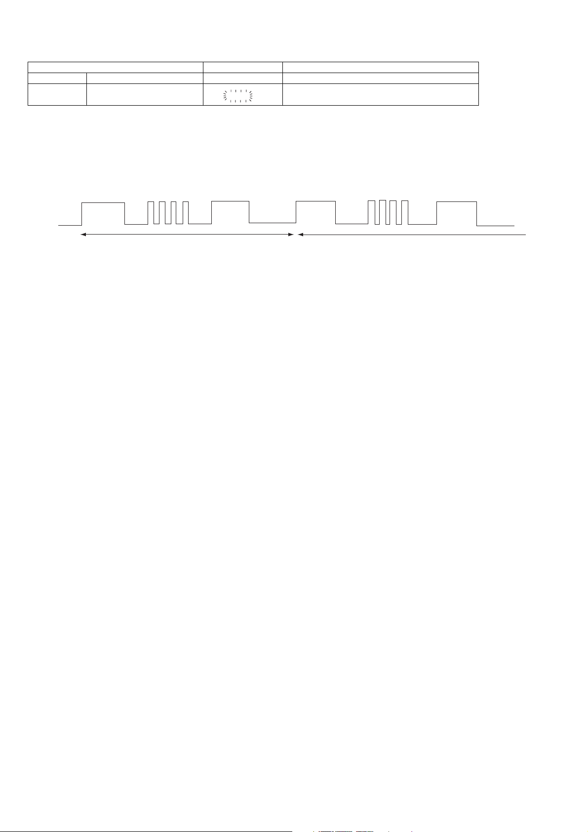
[3] Standard Specification Of Stereo System Error Message Display Contents
Error Contents DISPLAY Notes
CD Focus Not Match/IL Time Over. ‘NO DISC’
TUNER PLL Unlock.
87.50
FM MHz
AMP abnormal detection and +B PROTECTION display
In case AMP abnormal detection or +B PROTECTION had occurred, the unit will automatically enter to stand-by
mode and Timer indicator will flashing as below.
Example: In case of speaker abnormal
PLL Unlock.
ON
TIMER
LED OFF OFF
NO NO. 1.1
NO. 1 : +B PROTECTION
NO. 2 : AMP abnormal
FLASHING FLASHING
OFF
NO. 2
1
FRAME
ON ON ON
OFF OFF OFF OFF
NO. 2
(REPEAT)
BEFORE TRANSPORTING THE UNIT
The following process need to be taken after set tapering/parts replacement.
1. Press the POWER ON/STAND-BY button to enter stand-by mode.
2. While pressing down the POWER button and the CD button, plug-in AC. The Micro Computer version number will
be displayed as "X7U10**".
3. Press the POWER button until "WAIT"--> "FINISHED" appears.
4. Unplug the AC cord and the unit is ready for transporting.
2 – 4
Page 11
XL-DK257N
CHAPTER 3.
MECHANICAL DESCRIPTION
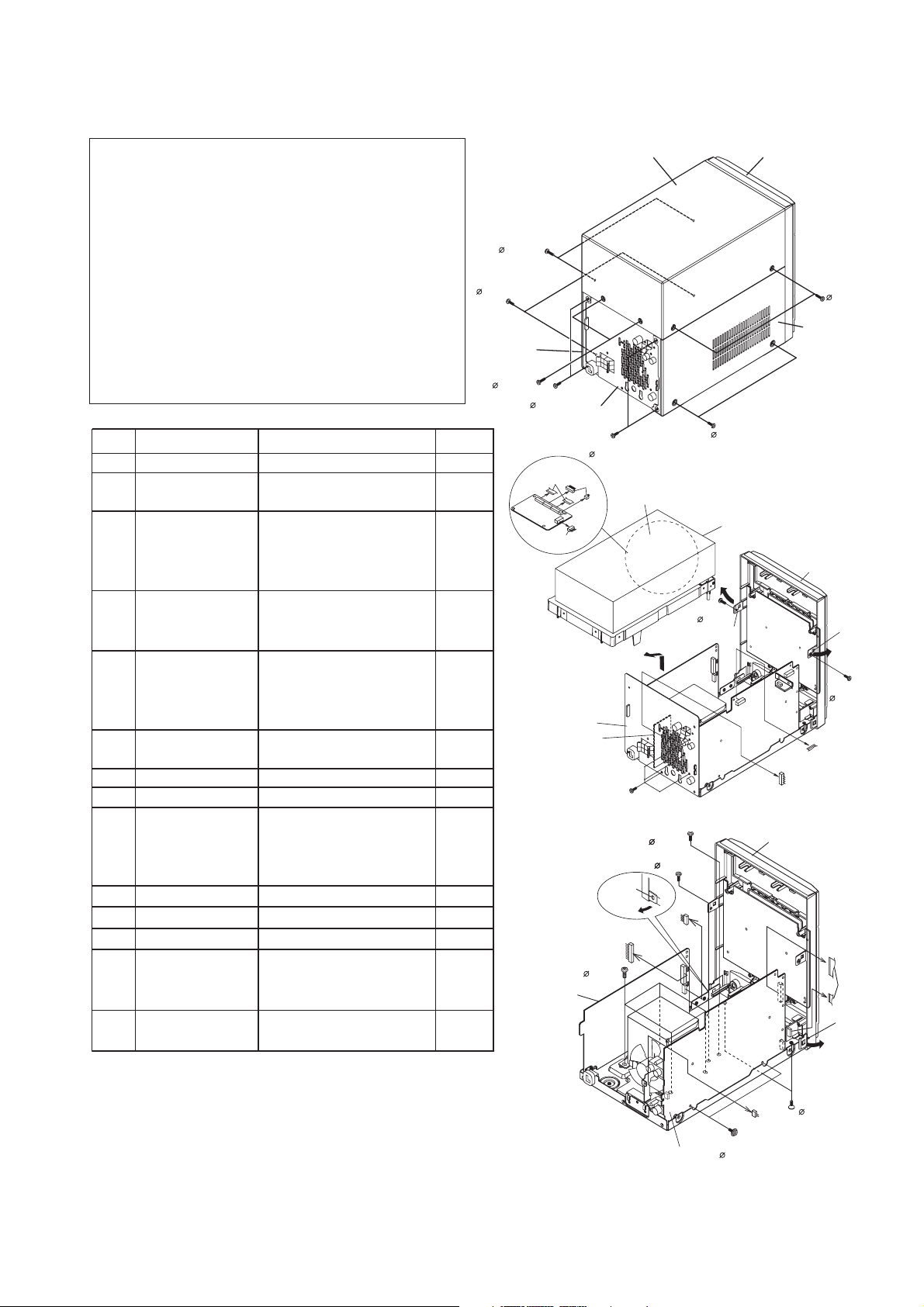
[1] Disassembly
Caution on disassembly
Follow the below-mentioned notes when disassembling
the unit and reassembling it, to keep it safe and ensure
excellent performance:
1) Take cassette tape and compact disc out of the unit.
2) Be sure to remove the power supply plug from the
wall outlet before starting to disassemble the unit.
3) Take off nylon bands or wire holders where they
need to be removed when disassembling the unit.
After servicing the unit, be sure to rearrange the
leads where they were before disassembling.
4) Take sufficient care on static electricity of integrated
circuits and other circuits when servicing.
STEP REMOVAL PROCEDURE FIGURE
1 Top Cabinet 1
2 Side Panel
(Left/Right)
3 CD Changer unit 2
4 Rear Panel with 2
Speaker PWB
5 Front Panel 3
6 Main PWB 3
7 Power PWB 3
8 Speaker PWB 4
9 Display PWB 5
10 USB PWB / SUB PWB 5
11 Jack PWB 5
12 Re-Flash PWB 6
13 CD MP3 PWB 7
14 CD Mechanism 7
1. Screw ............................(A1) X 6
1. Screw ............................(B1) X 8
1. Screw ............................(C1) X 2
2. Hook .............................. (C2) X 2
3. Socket ...........................(C3) X 3
4. Flat Cable ...................... (C4) X 2
1. Screw ............................(D1) X 4
2. Socket ...........................(D2) X 1
3. Flat Cable ...................... (D3) X 1
1. Screw ............................(E1) X 3
2. Flat Cable ...................... (E2) X 2
3. Socket ...........................(E3) X 1
4. Hook .............................. (E4) X 2
1. Screw ............................(F1) X 3
2. Socket ........................... (F2) X 2
1. Screw ............................(G1) X 4
1. Screw ............................(H1) X 2
1. Knob ...............................(J1) X 1
2. Nut..................................(J2) X 1
3. Washer...........................(J3) X 1
4. Screw .............................(J4) X 6
1. Screw ............................(K1) X 2
1. Screw ............................ (L1) X 1
1. Screw ........................... (M1) X 1
1. Screw ............................(N1) X 3
2. Flat Cable ...................... (N2) X 2
3. Socket ...........................(N3) X 1
1. Screw ............................(P1) X 4
2. Screw ............................(P2) X 4
1
8
(A1)x2
3x12mm
(B1)x2
3x10mm
Side Panel
(Right)
(A1)x2
3x12mm
(B1)x2
3x10mm
(C4)x2
(C3)x1
Rear Panel
Speaker PWB
Power PWB
Rear Panel
(C3)x2
(G1)x4
4x6mm
(B1)x2
3x10mm
(D1)x4
3x10mm
(E4)x1
PULL
(F2)x1
Top Cabinet
Figure 1
CD MP3 PWB
Figure 2
(E1)x1
3x6mm
(F1)x1
3x6mm
CD Changer Unit
(C1)x1
3x10mm
(E3)x1
(B1)x2
3x10mm
PULL
Hook
(C2)x1
Front Panel
(D2)x1
Front panel
Side Panel
(Left)
Front Panel
(D3)x1
PULL
(A1)x2
3x12mm
Hook
(C2)x1
PULL
(C1)x1
3x10mm
(E2)x2
Hook
(E4)x1
Note:
After removing the connector for the optical pickup from
the connector, wrap the conductive aluminium foil around
the front end of the connector so as to protect the optical
pickup from electrostatic damage.
3 – 1
Main PWB
Figure 3
(F1)x2
3x10mm
(F2)x1
(E1)x2
3x10mm
Page 12
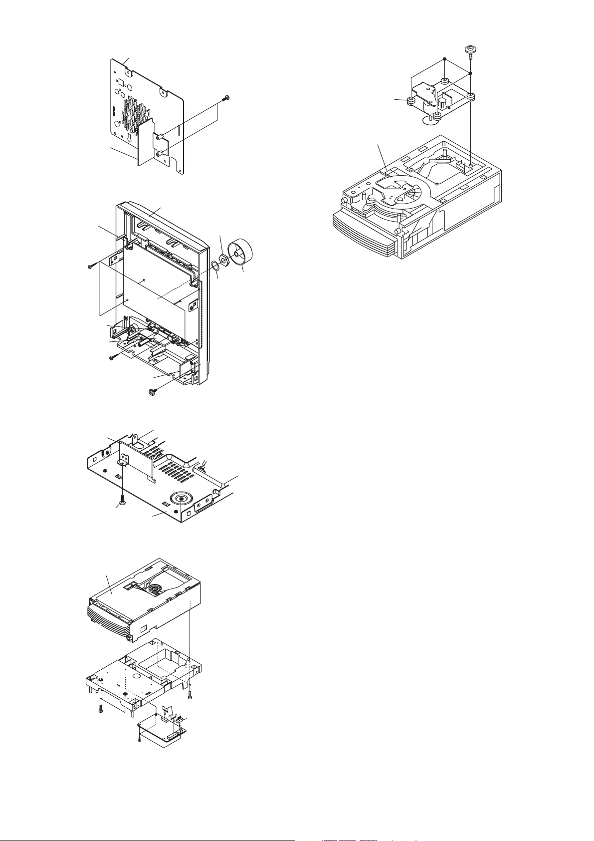
XL-DK257N
Speaker PWB
Display PWB
(J4)x6
Ø2.6x10mm
SUB PWB
USB PWB
Rear Panel
Figure 4
Front Panel
(J2)x1
(J3)x1
(H1)x2
Ø3x10mm
(J1)x1
CD Mechanism
CD Changer Unit
Figure 8
(P2)x4
Special
Ø2.6x10mm
Re-Flash PWB
(M1)x1
Ø3x10mm
CD Changer
Unit
(K1)x2
Jack PWB
(L1)x1
Special
Figure 5
Main Chassis
Figure 6
(P1)x2
Ø3x10mm
(N1)x3
Ø3x10mm
Figure 7
(N2)x2
(P1)x2
Ø3x10mm
(N3)x1
3 – 2
Page 13
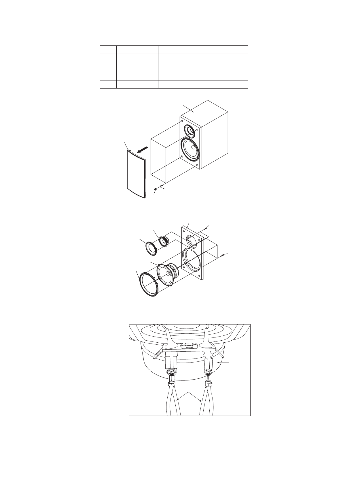
XL-DK257N
STEP PROCEDURE FIGURE
1 Woofer 1. Net Frame Ass’y............ (A1) X 1
REMOVAL
9, 10
2. Catching Holder............. (A2) X 4
3. Screw ............................ (A3) X 4
4. Screw ............................ (A4) X 4
2 Tweeter 1. Screw ............................ (B1) X 2
Speaker Box
Net Frame Ass’y
(A1) x1
(A3)x4
(A2)x4
Ø4x20mm
10
Figure 9
Tweeter Ring
Woofer
Woofer Ring
LOCKING
TA B
Tweeter
Front Board
Figure 10
SPEAKER
WIRE
(B1)x2
Ø3x14mm
(A4)x4
Ø3.5x14mm
SPEAKER
UNIT
LOCKING TAB
CAUTION TO REMOVE SPEAKER UNIT :
PRESS THESE LOCKING TABS TO RELEASE SPEAKER WIRE
3 – 3
Page 14
XL-DK257N
CHAPTER 4. DIAGRAMS
[1] Block Diagram
Figure 1: BLOCK DIAGRAM (1/2)
4 – 1
Page 15
XL-DK257N
120V/60Hz
Figure 2: BLOCK DIAGRAM (2/2)
4 – 2
Page 16
XL-DK257N
[2] CD Block Diagrams
Figure 4-3: CD BLOCK DIAGRAM (1/2)
4 – 3
Page 17
XL-DK257N
PA016AW
Figure 4-4: CD BLOCK DIAGRAM (2/2)
4 – 4
Page 18
XL-DK257N
FOO
TRO
1
9
10
2
9
13
DMO
FOO
9
13
FOO
DMO
TEI
RFO
FOO
9
6
89
9
FOO
6
TEI
9
FOO
DMO
LPFO
TMAX
13
76
74
67
66
65
BCKI
AIN
LRCKI
89
RFO
7
8
614
5
1
6
1
4
1
619
10115
CHAPTER 5.
CIRCUIT DESCRIPTION
[1] Waveforms Of Servo Circuit
IC1 IC1
IC1 IC1
IC1 IC1
IC1
IC1
IC1
IC1
IC1
IC1
IC1 IC1
IC1
IC1
IC1 IC1
IC1
5 – 1
Page 19
[2] Voltage
IC1
PIN
VOLTAGE
NO
1 0.02 26 0.01 51 1.53 76 3.26
2 1.63 27 1.52 52 0.03 77 1.63
3 0.76 28 3.03 53 3.27 78 0.98
4 0.70
5 0.59 30 1.52 55 0.03 80 1.74
6 0.70
7 1.63 32 3.27 57 1.53 82 1.63
8 3.27 33 0.03 58 3.27 83 1.68
9 1.63 34 4.53 59 0.04 84 1.63
10 1.63 35 1.53 60 3.27 85 1.62
11 1.63 36 0.01 61 0.03 86 1.64
12 1.63 37 3.25 62 0.03 87 1.66
13 1.63 38 2.41 63 0.03 88 1.62
14 0.01 39 2.14 64 0.03 89
15 0.52 40 2.59 65 1.62 90 3.27
16 0.55 41 2.25 66 1.65 91 3.25
17 0.01 42 0.61 67 3.24 92 0.01
18 0.01 43 3.25 68 1.49 93 0.02
19 1.11 44 0.04 69 0.02 94 1.63
20 0.36 45 0.04 70 1.63 95 1.63
21 0.26 46 0.04 71 3.26 96 1.63
22 0.01 47 0.04 72 1.61 97 1.63
23 0.26 73 1.31 98 1.63
24 0.34 49 1.64 74 0.02 99 1.64
25 0.54 50 1.65 75 1.38 100 1.63
PIN
VOLTAGE
NO
29 1.52 54 0.03 79 0.02
31 0.01 56 3.27 81 1.63
48 0.10
PIN
NO
VOLTAGE
PIN
NO
VOLTAGE
XL-DK257N
0.50
IC2
PIN
VOLTAGE
NO
1 3.18 10 3.27 19 3.20 28 7.09
2 3.17 11 1.63 20 3.20 29 0.01
3 3.19 12 1.63 21 0.01 30 1.63
4 3.20 13 1.63 22 0.01 31 2.24
5 3.19 14 1.63 23 0.01 32 3.15
6 3.18 15 1.63 24 0.01 33 3.16
7 0.00 16 1.63 25 0.00 34 2.69
8 4.39 17 1.62 26 7.03 35 3.16
9 7.08 18 1.62 27 7.08 36 3.16
Q1 Q2 Q3 Q4
PIN
VOLTAGE
NO
E 3.26 E 5.05 E 1.48 E 0.01
C 0.89 C 3.26 C 3.26 C 0.02
B 4.37 B 4.37 B 2.17 B 3.11
Q5
PIN
VOLTAGE
NO
E 5.08
C 5.05
B
4.37
PIN
VOLTAGE
NO
PIN
VOLTAGE
NO
Q8
PIN
VOLTAGE
NO
E 0.00
C 0.04
B
2.98
PIN
NO
PIN
NO
VOLTAGE
VOLTAGE
PIN
NO
PIN
NO
VOLTAGE
VOLTAGE
5 – 2
Page 20
XL-DK257N
IC701 IC601 IC705
VOLTAGE
PIN
NO
1 2.60m 51 3.50m 1 4.10 1 8.43
2 2.60m 52 -0.20m 2 4.10 2 8.49
3 3.13 53 1.88 3 4.10 3 3.77
4 3.13 54 3.28 4 0.40m 4 2.39
5 2.00m 55 3.04 5 4.10 5 0.49
6 3.12 56 2.80m 6 4.12 6 0.49
7 3.13 57 2.30m 7 4.10 7 0.49
8 1.30m 58 2.00m 8 4.12 8 0.49
9 0.50m 59 2.80m 9 4.12
10 0.37 60 2.80m 10 4.11
11 0.65 61 2.80m 11 4.12
12 3.21 62 3.13 12 0.40m
13 1.46 63 1.80m 13 0.40m
14 0.20m 64 0.70m 14 0.40m 1 5.01
15 1.35 65 2.00m 15 3.13 2 5.00
16 3.15 66 2.40m 16 3.13 3 4.88
17 3.15 67 3.04 17 3.13 4 0.70m
18 1.15 68 0.60m 18 9.28 5 4.90
19 1.40m 69 1.10m 19 9.28 6 5.00
20 3.11 70 3.28 20 4.10 7 5.02
21 3.28 71 33.80m 21 4.12 8 10.00
22 1.30m 72 3.13 22 4.12
23 2.30m 73 3.13 23 4.11
24 2.60m 74 2.90m 24 4.12
25 0.90m 75 2.80m 25 4.12
26 1.40m 76 2.10m 26 4.10
27 3.21 77 1.10m 27 4.12 1 2.02
28 3.13 78 3.13 28 4.11 2 216.70m
29 3.21 79 1.50m 29 0.50m 3 2.02
30 3.21 80 3.11 30 4.11 4 -1.80m
31 1.48 81 2.70m 31 4.11 5 2.03
32 4.80m 82 3.11 32 4.11 6 2.04
33 2.13 83 4.90m 7 2.02
34 0.86 84 48.00m 8 5.07
35 4.40m 85 3.28
36 4.50m 86 3.13
37 4.10m 87 2.70m
38 24.20m 88 2.90m
39 23.70m 89 3.10m 1 2.39 13 -26.81
40 4.30m 90 2.00m 2 -0.94 14 -6.32
41 0.90m 91 3.28 3 -0.94 15 -5.91
42 4.30m 92 3.18 4 -0.90 16 -0.81
43 3.80m 93 3.18 5 0.40m 17 -26.60
44 4.20m 94 3.18 6 -26.65 18 -26.60
45 4.20m 95 3.18 7 260.90m 19 0.00
46 3.12 96 1.30m 8 -0.80 20 -0.90
47 3.30m 97 3.18 9 -6.02 21 -0.30m
48 3.70m 98 53.50m 10 -6.53 22 -0.30m
49 3.90m 99 3.13 11 -26.71 23 -0.93
50 3.20m 100 2.90m 12 -14.31
(V)
PIN
NO
VOLTAGE
(V)
VOLTAGE
PIN
NO
PINNOVOLTAGE
(V)
(V)
PIN
NO
PINNOVOLTAGE
PINNOVOLTAGE
IC901
PINNOVOLTAGE
VOLTAGE
IC604
IC603
(V)
(V)
(V)
(V)
5 – 3
Page 21
XL-DK257N
IC702
VOLTAGE
PIN
NO
1 -26.44 33 -26.42
2 -26.40 34 -28.77
3 -26.40 35 -26.41
4 -26.40 36 -26.40
5 3.24 37 -26.41
6 3.20 38 -24.06
7 3.27 39 -17.00
8 3.24 40 -26.40
9 0.00 41 -24.07
10 0.00 42 -9.89
11 3.29 43 -26.40
12 1.51 44 -9.98
13 1.51 45 -17.00
14 0.00 46 -12.34
15 -24.10 47 -9.94
16 -28.77 48 -26.40
17 -28.78 49 -26.42
18 -28.77 50 -24.06
19 -28.77 51 -14.67
20 -28-75 52 -12.36
21 -28.77 53 -28.76
22 -28.77 54 -28.76
23 -21.70 55 -28.76
24 -28.97 56 -28.75
25 -26.40 57 -26.45
26 -28.77 58 -26.41
27 -28.76 59 -26.41
28 -28.76 60 -26.40
29 21.71 61 -26.40
30 -24.06 62 -26.40
31 -24.07 63 -26.40
32 -24.07 64 -26.40
(V)
PIN
NO
VOLTAGE
(V)
IC851 IC852
PIN
NO
VOLTAGE
(V)
PIN
NO
VOLTAGE
(V)
1 5.10 1 13.24
2 13.00 2 88.4m
3 17.60 3 4.76
m01.01-4
08.615
00.016
64.87
Q905IC853
PIN
NO
VOLTAGE
PIN
NO
VOLTAGE
1 5.07 D 35.10
2 5.07 S 26.53
3 3.28 G 31.77
39.14
m05.01-5
m04.01-6
m02.01-7
8 -10.20m
Q901
PIN
NO
VOLTAGE
D 27.82
S 35.68
G 30.91
5 – 4
Page 22

XL-DK257N
-MEMO-
5 – 5
Page 23
XL-DK257N
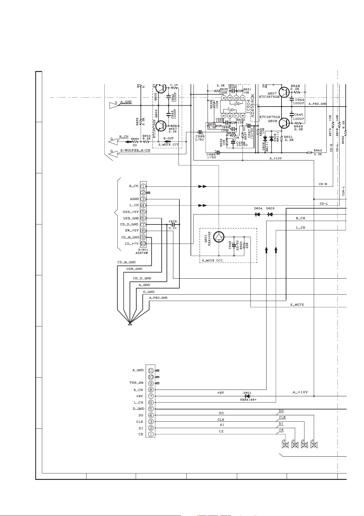
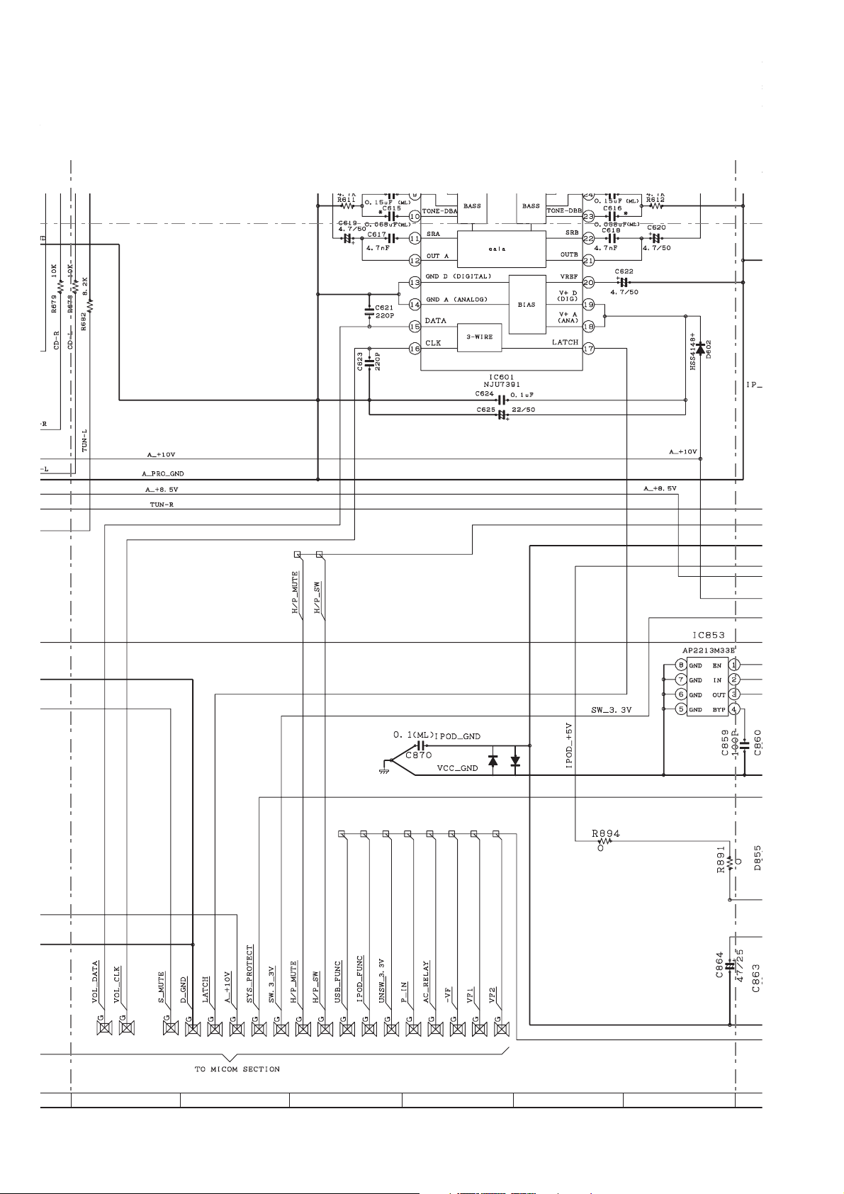
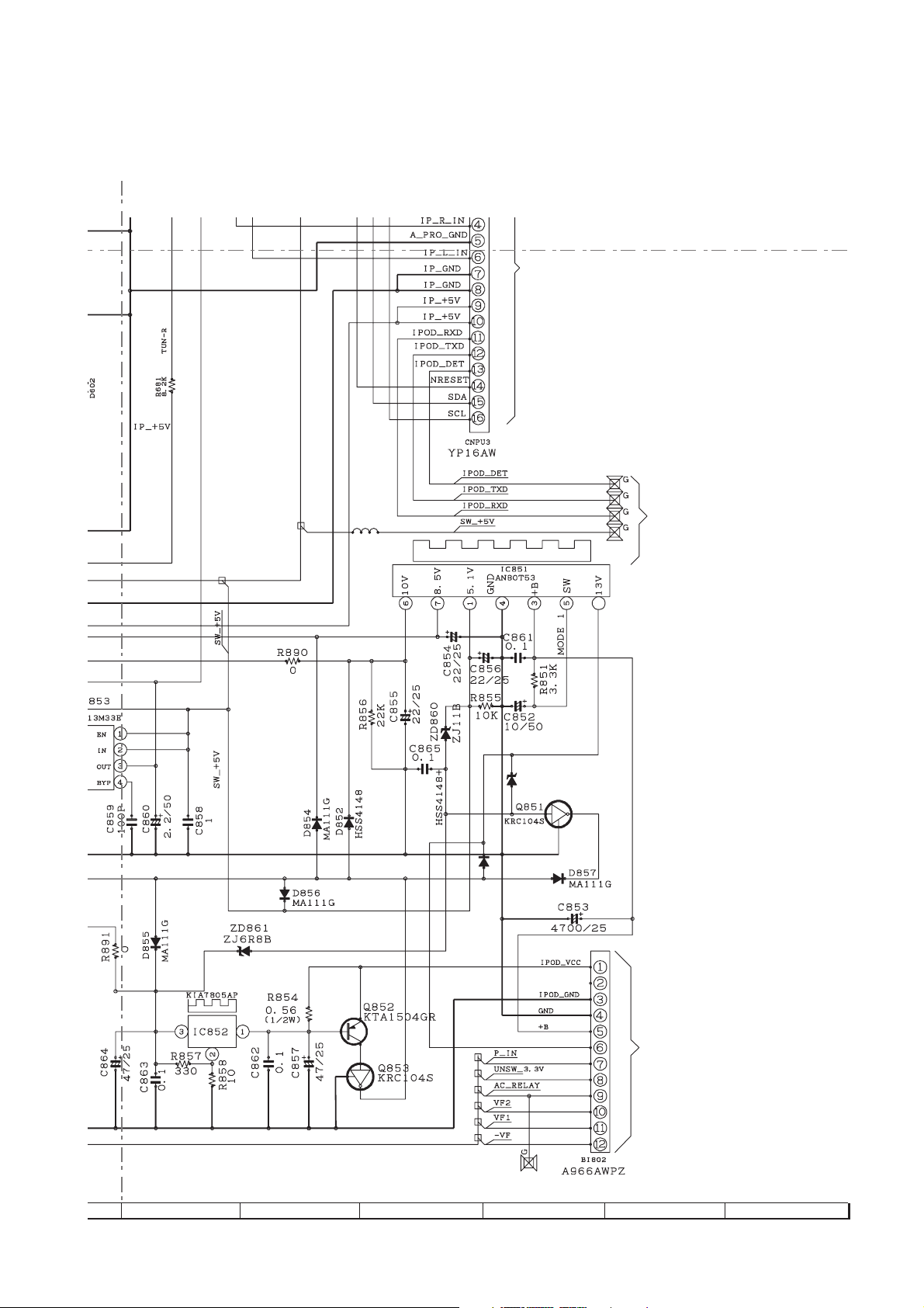
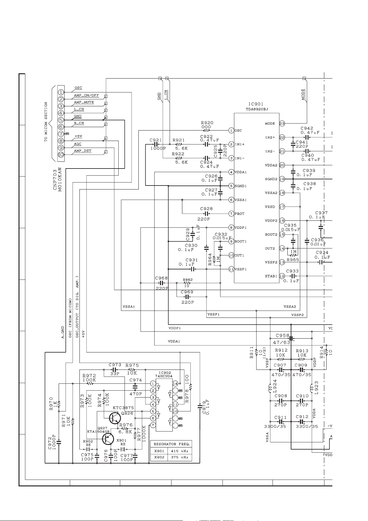
CHAPTER 6. CIRCUIT SCHEMATICS AND PARTS LAYOUT
[1] Notes On Schematic Diagram
•Resistor:
To differentiate the units of resistors, such symbol as
K and M are used: the symbol K means 1000 ohm
and the symbol M means 1000 kohm and the
resistor without any symbol is ohm-type resistor.
Besides, the one with “Fusible” is a fuse type.
• Capacitor:
To indicate the unit of capacitor, a symbol P is used:
this symbol P means pico-farad and the unit of the
capacitor without such a symbol is microfarad. As to
electrolytic capacitor, the expression “capacitance/
withstand voltage” is used.
(CH), (TH), (RH), (UJ): Temperature compensation
(ML): Mylar type
(P.P.): Polypropylene type
REF. NO DESCRIPTION POSITION
SW701 POWER ON/STAND-BY ON—OFF
SW702 TRAY OPEN/CLOSE ON—OFF
SW703 PLAY/PAUSE ON—OFF
SW704 STOP ON—OFF
SW705 CD ON—OFF
SW706 iPOD ON—OFF
SW707 TUNER (BAND) ON—OFF
SW708 AUDIO IN ON—OFF
VR701 VOLUME MAX—MIN
• Schematic diagram and Wiring Side of P.W.Board
for this model are subject to change for
improvement without prior notice.
• The indicated voltage in each section is the one
measured by Digital Multimeter between such a
section and the chassis with no signal given.
1. In the tuner section,
indicates AM
indicates FM stereo
2. In the CD section, the CD is stopped.
• Parts marked with “ ” ( ) are
important for maintaining the safety of the set. Be
sure to replace these parts with specified ones for
maintaining the safety and performance of the set.
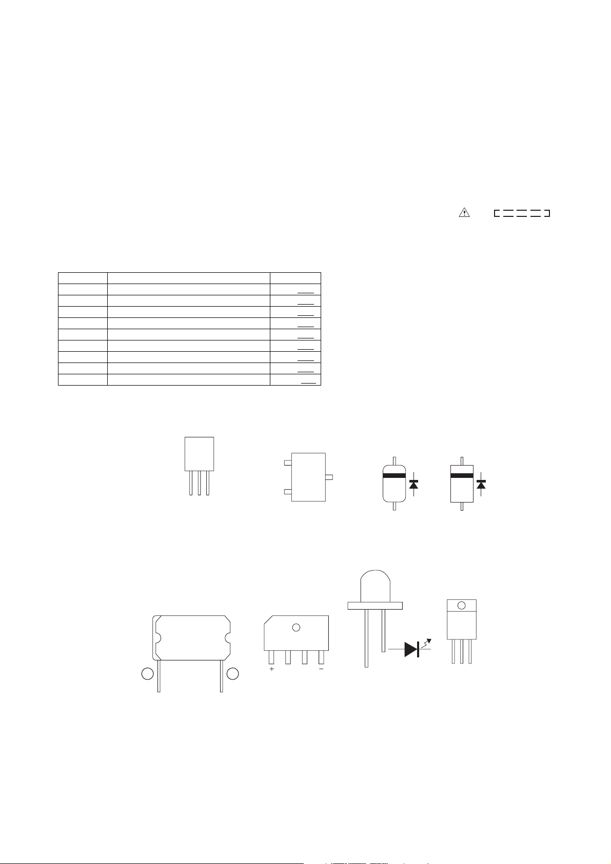
[2] Types Of Transistor And LED
FRONT
VIEW
ECB
(S)(G)(D)
(1)(2)(3)
KTA1271 Y
KTA1274 Y
FRONT
VIEW
123
TDA8920
KTC3199 GR
KTC3203 Y
KTA1266 GR
B
(3)
VIEW
E
(1)
KRA102 S
KRC107
KRC102 S
KRC104 S
KTA1504 GR
KTC3875 GR
KTA1544 T
KRA107 S
FRONT
VIEW
AC AC
10XB60F
TOP
(2)
TOP VIEWTOP VIEW
C
HSS4148
FRONT
VIEW
343VC3F
503BC2E30
1N4004S
DRL204F
MA 111
FRONT
VIEW
123
KIA7805A
NTP18N06LG
6 – 1
Page 24
XL-DK257N
[3] Schematic Diagram
A
ZJ15B
NTP18N06
GD1A4
22/100 22/100
GD1A4
B
C
TO AMPLIFIER SECTION
1K
10K
0.22
ZJ24B
2.2
GD1A4
ZJ27D
ZJ1SB
ZJ5R1B
22K
560
0.22
D
NTP18N06
E
F
47/10
47/10
100/16
G
TO MICOM SECTION
H
1
23456
Figure 6-1: MAIN SCHEMATIC DIAGRAM (1/6)
6 – 2
Page 25
FROM POWER SECTION
XL-DK257N
0.22
LUG2
A980AW
2.7K
C632
4700pF
5.6K
5.6K
6.8K
2.7K
7
8 9 10 11 12
Figure 6-2: MAIN SCHEMATIC DIAGRAM (2/6)
6 – 3
Page 26
XL-DK257N
6.8K
FROM HEADPHONE PWB-A4
2.7K
C633
4700pF
TO CHASSIS
TO MICOM
SECTION
13
14 15 16 17 18
TO IPOD SECTION
Figure 6-3: MAIN SCHEMATIC DIAGRAM (3/6)
6 – 4
Page 27
XL-DK257N
A
TO MICOM SECTION
B
C
TO CD MP3
IN4004S IN4004S
D
E
F
G
CNP301
ZX11AW
H
1
23456
Figure 6-4: MAIN SCHEMATIC DIAGRAM (4/6)
6 – 5
Page 28
XL-DK257N
2.7K
MA111G
MA111G
GND
7
8 9 10 11 12
D905
D906
Figure 6-5: MAIN SCHEMATIC DIAGRAM (5/6)
6 – 6
Page 29
XL-DK257N
2.7K
C633
4700pF
TO MICOM
SECTION
TO IPOD SECTION
JP41
100µH
ZD862
ZJ15B
D851
HSS4148
TO MICOM SECTION
2
13
+13V
FROM POWER SECTION
FROM CLAMP SECTION
14 15 16 17 18
Figure 6-6: MAIN SCHEMATIC DIAGRAM (6/6)
6 – 7
Page 30
XL-DK257N
A
B
AMPLIFIER SECTION
C
D
E
F
13
12
Z2130SCT5T
Z2130SCT5T
G
9
8
H
1
23456
Figure 6-7: AMPLIFIER & SPEAKER SCHEMATIC DIAGRAM (1/2)
6 – 8
Page 31

A523WJ
XL-DK257N
Z2130SCT5T
GND
(CHASSIS)
L921
Z0055
2
3
1
4
L920
Z0055
2
3
1
4
SPEAKER PWB-B2
7
8 9 10 11 12
Figure 6-8: AMPLIFIER & SPEAKER SCHEMATIC DIAGRAM (2/2)
6 – 9
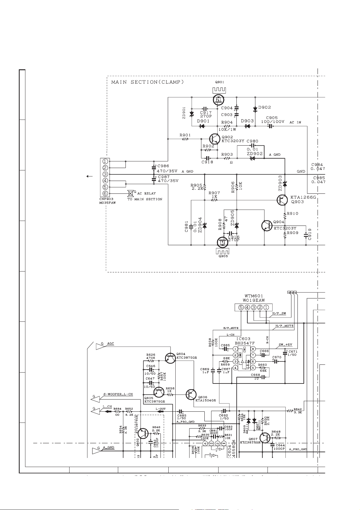
Page 32

XL-DK257N
P
P
A
B
C
TO MAIN SECTION (CLAMP)
D
CHASSIS GND
1.3V
E
TO MAIN SECTION
F
82
G
H
1
23456
Figure 6-9: POWER SCHEMATIC DIAGRAM (1/2)
6 – 10
Page 33

XL-DK257N
PT801
PA105AW
7
PA078AW
8 9 10 11 12
Figure 6-10: POWER SCHEMATIC DIAGRAM (2/2)
6 – 11
Page 34

XL-DK257N
P
0
0
A
B
C
D
VOLUME LED LIGHT-UP PWB-B3
E
F
RP767
680
(1/4)
270
100
100
G
H
1
23456
Figure 6-11: DISPLAY & VOLUME LED LIGHT-UP SCHEMATIC DIAGRAM (1/2)
6 – 12
Page 35

XL-DK257N
270P
1000P
1000P
7
Figure 6-12: DISPLAY & VOLUME LED LIGHT-UP SCHEMATIC DIAGRAM (2/2)
8 9 10 11 12
6 – 13
Page 36

XL-DK257N
A
B
C
D
MICOM SECTION
E
F
CNP701B
WZY18AW
G
H
1
23456
Figure 6-13: MICOM & HEADPHONE SCHEMATIC DIAGRAM (1/6)
6 – 14
Page 37

MICOM REFLASH PWB-A7
SYSTEM MICOM REFLASH PWB
TO EXT JIG
XL-DK257N
FROM DISPLAY SECTION
2.7K
7
8 9 10 11 12
Figure 6-14: MICOM & HEADPHONE SCHEMATIC DIAGRAM (2/6)
G
6 – 15
Page 38

XL-DK257N
HEADPHONE PWB-A4
HEADPHONE
D714
MA111
D715
MA111
5P52147
TO MAIN SECTION
B026AW
TO MAIN SECTION
TO CD MP3 PWB-D
G
13
14 15 16 17 18
O CD MP3 PWB-D
Figure 6-15: MICOM & HEADPHONE SCHEMATIC DIAGRAM (3/6)
6 – 16
Page 39

XL-DK257N
CNP701B
WZY18AW
A
B
C
D
E
F
G
H
1
23456
Figure 6-16: MICOM & HEADPHONE SCHEMATIC DIAGRAM (4/6)
6 – 17
Page 40

XL-DK257N
N
T
2.7K
MA111G
FROM MAIN SECTIO
(AUDIO PRO OUTPU
7
8 9 10 11 12
Figure 6-17: MICOM & HEADPHONE SCHEMATIC DIAGRAM (5/6)
6 – 18
Page 41

XL-DK257N
MA111G
TO CD MP3 PWB-D
N SECTION
O OUTPUT)
TO AMP SECTION
13
14 15 16 17 18
Figure 6-18: MICOM & HEADPHONE SCHEMATIC DIAGRAM (6/6)
6 – 19
Page 42

XL-DK257N
A
B
C
D
E
F
G
H
1
23456
GND
(CHASSIS)
Figure 6-19: iPOD SCHEMATIC DIAGRAM (1/2)
6 – 20
Page 43

XL-DK257N
7
8 9 10 11 12
Figure 6-20: iPOD SCHEMATIC DIAGRAM (2/2)
6 – 21
Page 44

XL-DK257N
A
B
C
D
E
F
G
H
1
23456
Figure 6-21: CD SERVO SCHEMATIC DIAGRAM (1/2)
6 – 22
Page 45

XL-DK257N
PA016AW
7
8 9 10 11 12
Figure 6-22: CD SERVO SCHEMATIC DIAGRAM (2/2)
6 – 23
Page 46

XL-DK257N
2
108642121416
6
[4] Charts Of Connecting Wires
A
B
FOR
MICOM EXTERNAL
DEVICE
MICOM REFLASH PWB-A5
CNPU2
CNPU1
12345678
12345678
DISPLAY PWB-B1
CNP701A
108642912111413161518
177531
118
CNS703
12
Bi703
12
FFC701
RDGYWHGYWH
GY
RDBLWHBLWHBLWHBLWHBLWH
C
D
SCREW TO
CHASSIS
E
F
CNS801
WH
BK
123456
12345 6
CNP801
CNP801
123456 7 891011
123456 7 891011
LUG 801
POWER PWB-A2
CNP805
AC POWER SUPPLY CORD
AC 120V ~ 60Hz
CNP802
CNS802
TO
CD PWB-D
(CNP5)
CNS601
BR
BK
GY
BK
435678921
GY
BK
GY
BK
GY
GY
WH
GY
WH
GY
RD
GY
12345 67
CNS702
12345 6 7 8
RDWHBKWHBKWHBK
WTM601
Bi901
BKGYBKGYBKGYBK
435678910 2 1
BR
15
FW601
WH
Bi601
WH
BK
WH
BK
WH
BK
WH
RD
LUG 2
SCREW TO
CHASSIS
18
177531
16
15
14
CNP701B
13
12
11
108642
9
Bi702
12345 6 7 89
RDBLWHBLWHBLWHBLWHBLWH
12 345 67 89101112
FFC705
18
8642
7531
CNP705
MAIN PWB-A1
Bi802
CNP903
123456
CNS903
123456
RDBLWHBLWH
BL
FFC702
TO
CD PWB-D
(CNP6)
CNP702
1357
2468910
12345
1
1
CNPU3
G
H
1
23456
Figure 6-23: WIRING CONNECTION (1/2)
6 – 24
Page 47

VOLUME LED LIGHT-UP PWB-B3
12
CNP703
TO
(MOTOR)
CD MECHANISM
TO
CD MOTOR PWB
XL-DK257N
FROM
MAIN PWB-A1
(Bi601)
FROM
MAIN PWB-A1
435678921
CNS601
435678921
CNP6
157531
(CNP702)
108642
97531
1357
2468
GYBKGYBKGYBKGYBKBR
CNP5
FFC705
81 1 10
GR
YL
OR
RD
BR
12345
CNS4
CNP4
12345
CNP3
CD PWB-D
WH
BL
WH
BL
WH
RD
123456
CNS2
CNP2
123456
CNP1
10864291211141316
TO
D PWB-D
(CNP6)
111
1357
9
2468
CNP702
CNPU3
12345678910
16
14
12
108642
CNP301
157531
13
11
9
CNS703
FFC301
PKGYBK
4321
Bi710
JK691
WH
JK902
ANTENNA
FM
GND
AM
116
AUDIO IN
SUBWOOFER
PRE-OUT
TUNER PACK
CNS710
PK
321
BK
WH
FW601
FFC102
HEADPHONE PWB-A4
CNP710
321
CNP708
15
LUG 4
JK703
JK701
AUDIO IN SOCKET
HEADPHONE SOCKET
SCREW TO CHASSIS
iPOD PWB-C
16
CNP102
1
WIRE
SCREW TO CHASSIS
FFC1
1
TO
CD PICK-UP
UNIT
FROM
iPOD EXTERNAL
DEVICE
16
COLOR TABLE
WH
RD
BK
BL
WHITE
RED
BLACK
BLUE
GY GRAY
BR BROWN
PK PINK
OR ORANGE
FFC301
108642
9117531
SPEAKER PWB-B2
12345
Bi902
CNS902
RD
1234
BL
WH
BL
12
3
4
CNP902
SLOT-IN
TO MAIN PWB-A1
(CNS703)
7
AMPLIFIER PWB-A3
12345 67 8 910
CNP703
SO901
R-CH
SPEAKER TERMINAL
L-CH
1234567
Bi903
RD
BLWHBLWHBL
8 9 10 11 12
Figure 6-24: WIRING CONNECTION (2/2)
6 – 25
TO SPEAKER SYSTEM
Page 48

XL-DK257N
[5] Wiring Side Of PWB
MAIN PWB-A1
A
B
2 4 6 8 10 12 1416 18
1357911131517
123
4
6
8
5
7
C
10 9 8 7 6 5 4 3 2 1
12 3 45 6 78 9
D
1357
7654321
246
E
ECB
F
D G S
ECB
D G S
ECB
23456789
1
10 11 12
G
23 45 61
Lead-free solder indication
Lead-free solder is used in the MAIN PWB.
Refer to "Precautions for handling lead-free solder" for instructions
H
and precautions.
1
23456
Figure 6-25: WIRING SIDE OF MAIN PWB (TOP VIEW) (1/2)
6 – 26
Page 49

XL-DK257N
10 12 14 16
2468
1113 15
13579
10
9
11
VIDEO OUT
8
1
2
113355779
2244668810
10 11 12
1234
SUBWOOFER
PRE-OUT
23456789101
7
8 9 10 11 12
Figure 6-26: WIRING SIDE OF MAIN PWB (TOP VIEW) (2/2)
6 – 27
Page 50

XL-DK257N
A
MAIN PWB-A1
B
JP46
C
D
E
F
G
H
1
23456
Figure 6-27: WIRING SIDE OF MAIN PWB (BOTTOM VIEW) (1/2)
6 – 28
Page 51

XL-DK257N
Lead-free solder indication
Lead-free solder is used in the MAIN PWB.
Refer to "Precautions for handling lead-free solder" for instructions
and precautions.
7
8 9 10 11 12
Figure 6-28: WIRING SIDE OF MAIN PWB (BOTTOM VIEW) (2/2)
6 – 29
Page 52

XL-DK257N
A
POWER PWB-A2
43
5
B
123
C
6
7
8
9
3
TF801
PT841
(SUB)
2
POWER TRANSFORMER
4
RL841
3
2
1
RELAY
1
1
2
D
E
F
G
Lead-free solder indication
Lead-free solder is used in the POWER PWB.
H
Refer to "Precautions for handling lead-free solder" for instructions
and precautions.
11 12 138910
POWER TRANSFORMER (MAIN)
PT801
BCE
1011
16 1714 15
123456
123456789
1
23456
Figure 6-29: WIRING SIDE OF POWER PWB (TOP VIEW)
6 – 30
Page 53

-MEMO-
XL-DK257N
6 – 31
Page 54

XL-DK257N
A
AMPLIFIER PWB-A3
B
C
78910
23456
1
D
E
2 4 6 8 10 12 14 1618 20 22
1 3 5 7 9 11131517192123
12345
F
1234567
G
Lead-free solder indication
Lead-free solder is used in the AMPLIFIER PWB.
H
Refer to "Precautions for handling lead-free solder" for instructions
and precautions.
1
23456
Figure 6-30: WIRING SIDE OF AMPLIFIER PWB (TOP VIEW)
6 – 32
Page 55

A
AMPLIFIER PWB-A3
B
C
XL-DK257N
D
E
F
G
Lead-free solder indication
Lead-free solder is used in the AMPLIFIER PWB.
H
Refer to "Precautions for handling lead-free solder" for instructions
and precautions.
1
23456
Figure 6-31: WIRING SIDE OF AMPLIFIER PWB (BOTTOM VIEW)
6 – 33
Page 56

XL-DK257N
A
HEADPHONE PWB-A4
AUDIO IN
B
C
D
321 54
32 1
FOR HEADPHONE ONLY
E
MICOM REFLASH PWB-A5
F
G
Lead-free solder indication
Lead-free solder is used in the HEADPHONE and MICOM REFLASH PWB.
H
Refer to "Precautions for handling lead-free solder" for instructions
and precautions.
123456 78
123456 78
1
23456
Figure 6-32: WIRING SIDE OF HEADPHONE AND MICOM REFLASH PWB (TOP VIEW)
6 – 34
Page 57

A
HEADPHONE PWB-A4
B
C
XL-DK257N
D
E
F
G
Lead-free solder indication
Lead-free solder is used in the HEADPHONE PWB.
H
Refer to "Precautions for handling lead-free solder" for instructions
and precautions.
1
23456
Figure 6-33: WIRING SIDE OF HEADPHONE PWB (BOTTOM VIEW)
6 – 35
Page 58

XL-DK257N
2
V
A
DISPLAY PWB-B1
FL701
252627282930313233343536373839404142434445464748495051
B
C
D
2 4 6 8 10 12 14 16 18
1
3 5 7 9 11 13 15 17
E
F
G
H
1
23456
Figure 6-34: WIRING SIDE OF DISPLAY PWB AND VOLUME LED LIGHT-UP (TOP VIEW) (1/2)
6 – 36
Page 59

FL701
XL-DK257N
12345678910111213141516171819202122232425262728
12
VOLUME LED LIGHT-UP PWB-B3
12
Lead-free solder indication
Lead-free solder is used in the DISPLAY PWB and VOLUME LED LIGHT-UP.
Refer to "Precautions for handling lead-free solder" for instructions
and precautions.
7
Figure 6-35: WIRING SIDE OF DISPLAY PWB AND VOLUME LED LIGHT-UP (TOP VIEW) (2/2)
8 9 10 11 12
6 – 37
Page 60

XL-DK257N
A
DISPLAY PWB-B1
B
C
D
E
F
VOLUME LED LIGHT-UP PWB-B3
G
H
1
Figure 6-36: WIRING SIDE OF DISPLAY PWB AND VOLUME LED LIGHT-UP (BOTTOM VIEW) (1/2)
23456
6 – 38
Page 61

XL-DK257N
Lead-free solder indication
Lead-free solder is used in the DISPLAY PWB and VOLUME LED LIGHT-UP.
Refer to "Precautions for handling lead-free solder" for instructions
and precautions.
7
Figure 6-37: WIRING SIDE OF DISPLAY PWB AND VOLUME LED LIGHT-UP (BOTTOM VIEW) (2/2)
8 9 10 11 12
6 – 39
Page 62

XL-DK257N
A
SPEAKER PWB-B2
B
C
D
E
1234
F
G
H
1
23456
Figure 6-38: WIRING SIDE OF SPEAKER (TOP VIEW)
Lead-free solder is used in the SPEAKER PWB.
Refer to "Precautions for handling lead-free solder" for
instructions and precautions.
SO901
SPEAKER TERMINAL
Lead-free solder indication
6 – 40
Page 63

A
SPEAKER PWB-B2
B
XL-DK257N
C
D
E
F
G
Lead-free solder indication
H
1
Figure 6-39: WIRING SIDE OF SPEAKER AND VOLUME LED LIGHT-UP PWB (BOTTOM VIEW)
23456
Lead-free solder is used in the SPEAKER PWB.
Refer to "Precautions for handling lead-free solder" for
instructions and precautions.
6 – 41
Page 64

XL-DK257N
A
iPOD PWB-C
B
R136
R139
IC101
R138
R135
R140
D107
CNP102
C114
C113
C111
C100
R137
R122
R123
R128
R129
R132
JP104
R107
R134
R133
R110
R113
R131
C104
Q100
C
D
R115
JP101
JP102
R118
E
C108
C110
C101
L101
D108
C118
F
D109
D105
R121
C112
R120
D104
R119
WIRE
G
Lead-free solder indication
Lead-free solder is used in the iPOD PWB.
H
Refer to "Precautions for handling lead-free solder" for instructions
and precautions.
1
23456
Figure 6-40: WIRING SIDE OF iPOD PWB (TOP VIEW)
6 – 42
Page 65

XL-DK257N
A
B
C
D
iPOD PWB-C
CNP101
E
F
G
H
1
23456
Figure 6-41: WIRING SIDE OF iPOD PWB (BOTTOM VIEW)
6 – 43
Page 66

XL-DK257N
2
A
CD PWB-D
1357
2468
B
123456789
1
C
D
21345
ECB
E
F
213456
4268
10 12 14 16
31579
G
H
1
23456
Figure 6-42: WIRING SIDE OF CD PWB (TOP VIEW) (1/2)
11 13 15
6 – 44
Page 67

XL-DK257N
4268
10
31579
12 14 16
13 15
Lead-free solder indication
Lead-free solder is used in the CD PWB.
Refer to "Precautions for handling lead-free solder" for instructions
and precautions.
7
8 9 10 11 12
Figure 6-43: WIRING SIDE OF CD PWB (TOP VIEW) (2/2)
6 – 45
Page 68

XL-DK257N
A
CD PWB-D
B
C49
C
C50
C51RA33
D
E
C10
C11
C12
C16
R7
C17
C48
C53
R38
C6
C9
RA14
R1
R2
R3
R5
R4
C7
C18
C20
C55
C8
C14
C13
C21
C19
C23
R37
C71
R55
C52
R34
C54
C24
C25
F
R10
R8
R9
R11
Q1
RA16
G
RA15
R6
C5
Lead-free solder indication
H
Lead-free solder is used in the CD PWB.
Refer to "Precautions for handling lead-free solder" for instructions
and precautions.
1
23456
Figure 6-44: WIRING SIDE OF CD PWB (BOTTOM VIEW) (1/2)
6 – 46
Page 69

C71
R55
C72
R56
XL-DK257N
R57
R44
R43
RA44
4
C24
C52
R34
C25
C26
C47
C27
JP4
IC1
C46
CA3
R16
R14
C44
C43
FB2
C45
RA4
C34
R20
C33
R39
C1
R25
JP3
RA5
C3
RA3
C41
FB1
C39
R21
R22
C38
C37
R23
R24
C36
C35
C30
C28
C29
C32
C31
CA4
C56
Q8
C49
C62
C58
C59
R40
Q3
R48
R53
C66
R51
R92
R46
R93
C64
Q4
RA45
Q5
R94
R54
C61
IC2
7
8 9 10 11 12
Figure 6-45: WIRING SIDE OF CD PWB (BOTTOM VIEW) (2/2)
6 – 47
Page 70

XL-DK257N
CHAPTER 7. FLOWCHART
[1] Troubleshooting
1. When the CD does not function
The CD section may not operate when the objective lens of the optical pickup is dirty. Clean the objective lens, and
check the playback operation. When this section does not operate even after the above step is taken, check the
following items.
Remove the cabinet and follow the troubleshooting instructions.
"Track skipping and/or no TOC (Table Of Contents) may be caused by build up of dust other foreign matter on the
laser pickup lens. Before attempting any adjustment make certain that the lens is clean. If not, clean it as mentioned
below."
Turn the power off.
Gently clean the lens with a lens cleaning tissue and a small amount of isopropyl alcohol.
Do not touch the lens with the bare hand.
Parts code
1. CD optical pickup Lens cleaner disc UDSKA0004AFZZ
HOW TO USE
1.
Using the brush in the cleaner cap, apply 1 or 2 drops of the cleaning fluid to the
brush on the CD cleaner disc which has the mark next to it.
2.
Place the CD cleaner disc onto the CD disc tray with the brush side down,then
press the play button.
3.
You will hear music for about 20 seconds and the CD player will automatically stop.
If it still play continuously, press the stop button.
CAUTION
The CD lens cleaner should be effective for 30-50 operations, however if the
brushes become worn out earlier then please replace the cleaner disc.
If the CD cleaner brushes become very wet then wipe off any excess fluid with a soft
cloth.
Do not drink the cleaner fluid or allow it contact with the eyes. In the event of this
happening then drink and / or rinse with clean water and seek medical advice.
The CD cleaner disc must not be used on car CD players or on computer CD-ROM
drives.
All rights reserved. Unauthorized duplicating, broadcasting and renting this product
is prohibited by law.
Cleaning fluid
Cleaner disc
2. When a CD cannot be played
2.1. Pressing the CD operation key is accepted, but playback does not occur.
1) Focus-RF system check
2) Tracking system check
3) Spin system check
4) PLL system check
5) Others
7 – 1
Page 71

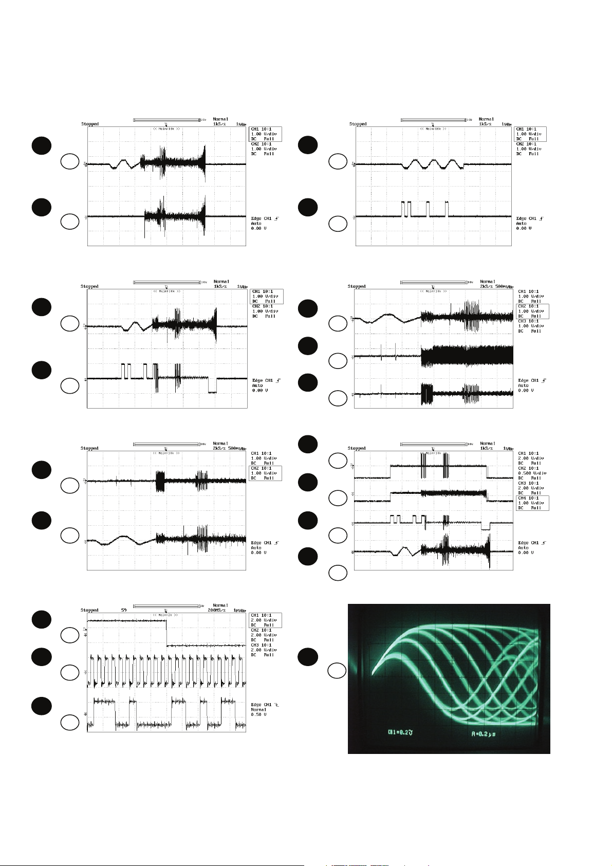
(1) Focus-RF system check.
9
1
2
FOO
TRO
9
6
4
5
1
TEI
RFO
FOO
RFO
Although a CD is inserted and the cover is closed, "NO DISC" is displayed.
1. Does the pickup move? No Sled motor (M2A).
Yes
2. Does the focus (lens) move up and down ?
(Waveform drawing Figure 1)
Yes
3. Is the laser lit ? No Check the laser diode driver Q1 peripheral circuit.
Yes
4. Is the turntable rotating ? No Spindle motor (M1A).
When a disc is loaded, start playback operation.
1. Is focus servo activated ?
(Waveform drawing Figure 2)
No Check the focus peripheral circuit.
No Pins 5, 9, 94 and 95 on IC1, Pins 1, 2, 15 and 16 on IC2.
Check the laser diode driver Q1 peripheral circuit.
XL-DK257N
Yes
2. Is the RF waveform normal ?
(Waveform drawing Figure 3)
Press the Tray1 CD Eject Button without inserting a disc, and try
starting the playback operation.
IC1
IC1
Figure 1
No If the level is not normal.
5
IC1
89
Figure 3
IC1
89
IC1
IC1
Figure 2
7 – 2
Page 72

XL-DK257N
9
6
4
1
FOO
TEI
1
6
9
FOO
DMO
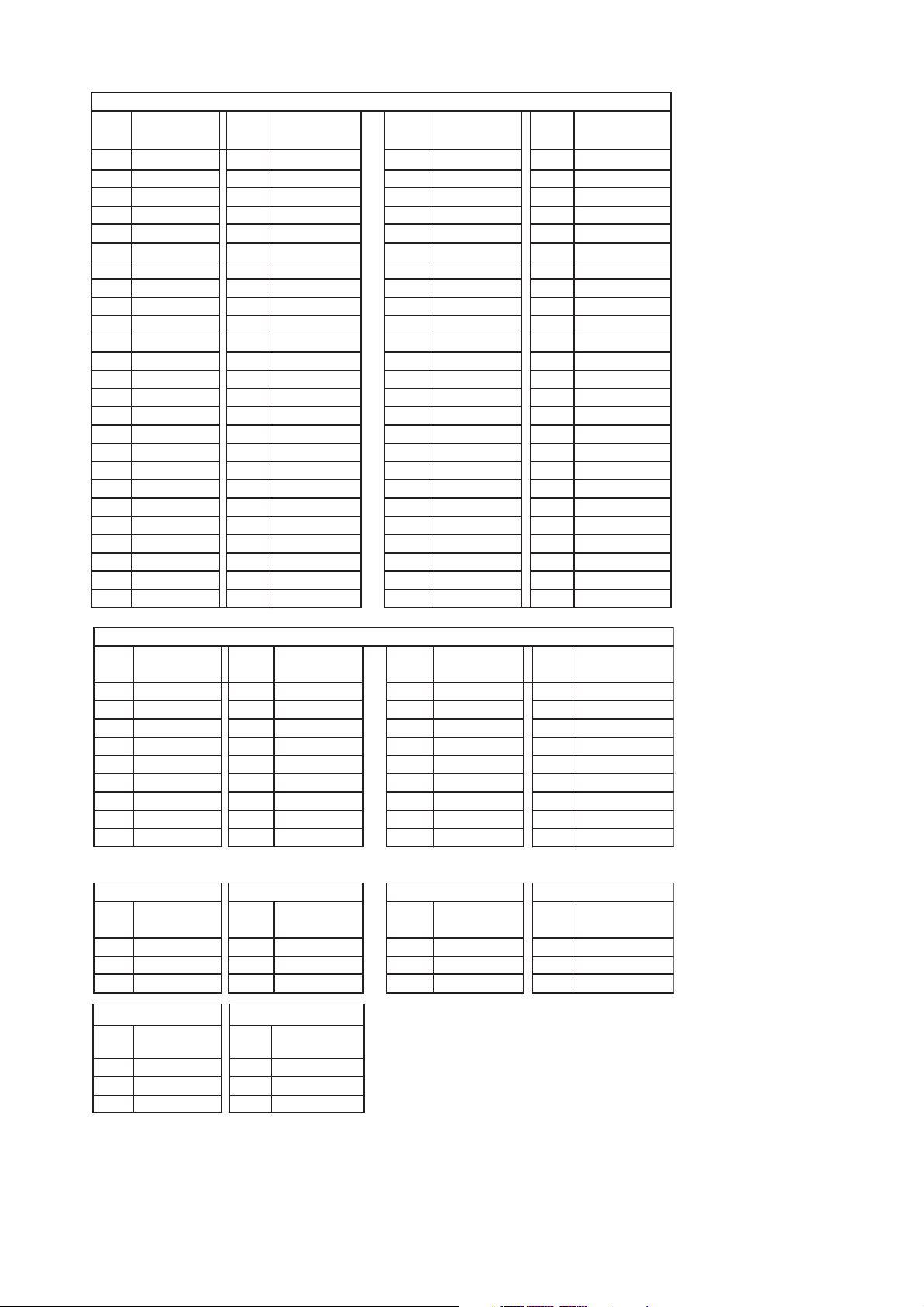
(2) Tracking system check.
Check the TE waveform at pin 6 on IC1.
If the waveform shown in Figure 4 appears and soon after NO
DISC appears ?
No
"Initialization" is possible, but play is not possible ?
No
"Initialization" is not possible. Data cannot be read. Check the VCO-PLL (Pins 72, 73, 74,
Yes
Yes
The tracking servo is not activated.
Check the peripheral circuits at pins 6, 7, 10, 98 and 100 on
IC1, pins 17, 18, 35 and 36 on IC2 and FFC1.
A normal jump operation cannot be completed or the
beginning of the track cannot be found.
Check the around pin 10 on IC1.
75, 76 and 78 on IC1) system.
IC1
IC1
Figure 4
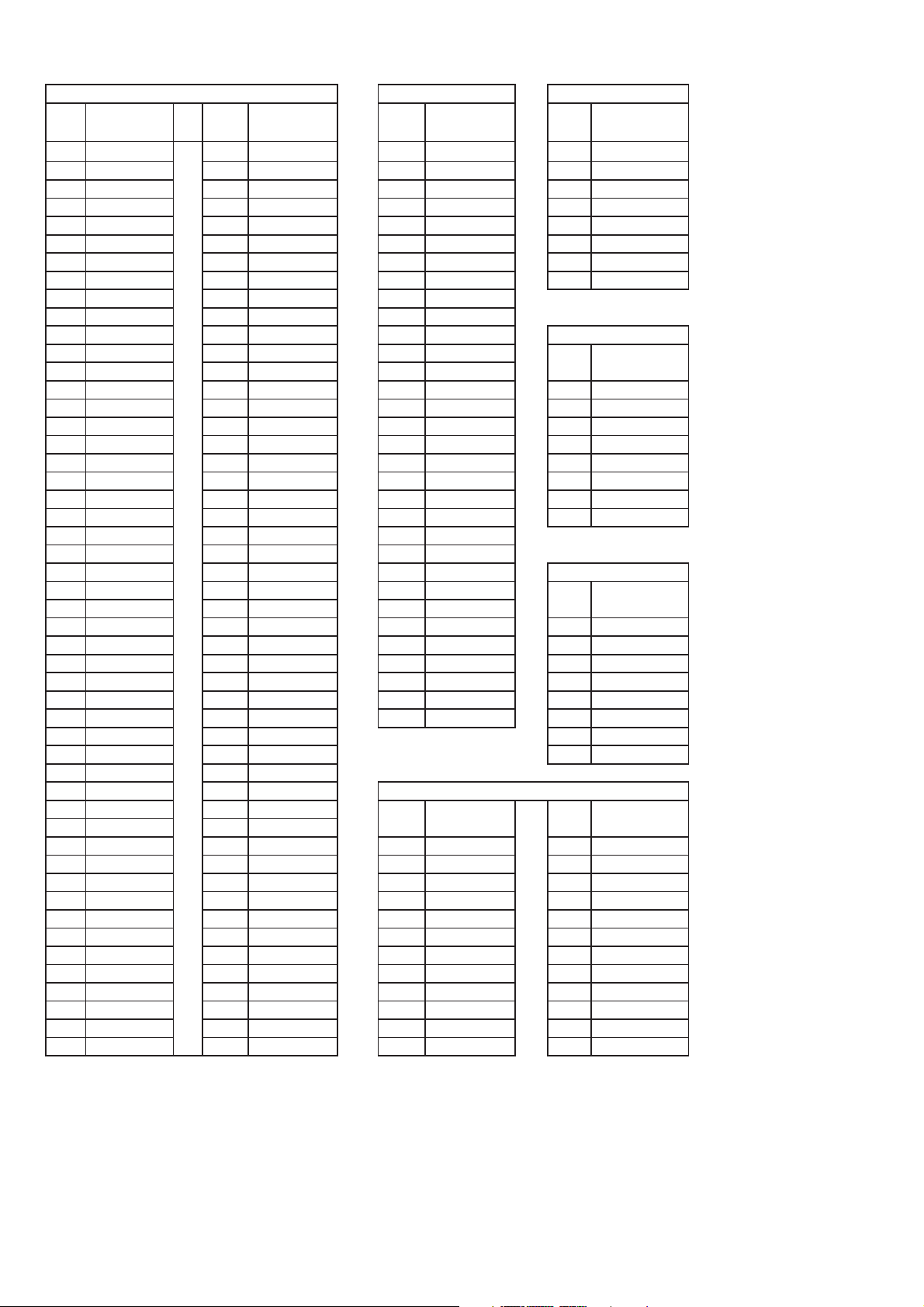
(3) Spin system check.
Press the OPEN/CLOSE switch without inserting a disc, and
then try starting the play operation.
1. The turntable rotates a little ?
(Waveform drawing Figure 5)
No
2. The turntable doesn't rotate. Check around pin 13 on IC1, pins 3, 4, 13 and 14 on IC2.
Yes
The spin driver circuit is OK.
IC1
IC1
Figure 5
7 – 3
Page 73

(4) PLL system check.
9
74
7
8
6
1
FOO
DMO
LPFO
TMAX
XL-DK257N
When a disc is loaded, start play operation.
The RF waveform is normal, but the TOC data cannot be read.
IC1
IC1
IC1
Check the TMAX waveform. (Figure 6)
IC1
Check around Pins 72, 73, 74, 75, 76 and 78 on IC1.
Figure 6
(5) Others.
The RF waveform is normal and the time is displayed
normally, but no sound is produced. Or the sound has
dropouts.
Is pin 65, 66 and 67 on IC1. (Figure 7) No There are too many error flags on a damaged disc which makes
error correction impossible.
Yes
If OK, Check the unit.
Check again using a known good disc.
9
IC1
10
IC1
11
IC1
65
67
66
LRCKI
BCKI
AIN
Figure 7
7 – 4
Page 74

XL-DK257N
CHAPTER 8. OTHER
[1] Function Table Of IC
IC2 VHILA6261//-1: Focus/Tracking/Spin/Sled Driver (LA6261)
Pin No. Terminal Name Function
1 FO+ BTL Output pin (+) for focus coil.
2 FO- BTL Output pin (-) for focus coil.
3 SP+ BTL Output pin (+) for spin motor.
4 SP- BTL Output pin (-) for spin motor.
5 SL- BTL Output pin (+) for slide motor.
6 SL+ BTL Output pin (-) for slide motor.
7 PGND1 Power GND for channels 1,2,3 and 4 (BTL).
8 REGIN Regulator pin (External PNP base).
9 PVCC1 Power for channels 1,2,3 and 4 (BTL). (SVCC short-crircuited)
10 REGOUT Regulator pin (External PNP collector).
11 VIN1 Input pin for channel 1
12* VIN1G Input pin for channel 1 (for gain control)
13 VIN2 Input pin for channel 2
14* VIN2G Input pin for channel 2 (for gain control)
15 VIN3 Input pin for channel 3
16* VIN3G Input pin for channel 3 (for gain control)
17 VIN4 Input pin for channel 4
18* VIN4G Input pin for channel 4 (for gain control)
19 FWD5 CH5 Output change pin (FWD). Logic input for bridge.
20 REV5 CH5 Output change pin (REV). Logic input for bridge.
21 VCONT5 Input pin for CH5 output voltage control.
22 FWD6 CH6 Output change pin (FWD). Logic input for bridge.
23 REV6 CH6 Output change pin (REV). Logic input for bridge.
24 VCONT6 Input pin for CH5 output voltage control.
25 VREFIN Reference voltage input pin.
26 SGND Signal system GND.
27 SVCC Signal system power (PVCC1 short - circuited).
28 PVCC2 Power for channel 5 and 6 (H bridge).
29 MUTE Input pin for BTL mute.
30 PGND2 Power GND for channels 5 and 6 (H bridge).
31 TR+ H bridge Output pin (+) for tray motor.
32 TR- H bridge Output pin (-) for tray motor.
33 CAM+ H bridge Output pin (+) for cam motor.
34 CAM- H bridge Output pin (-) for cam motor.
35 TR+ BTL Output pin (+) for tracking coil.
36 TR- BTL Output pin (-) for tracking coil.
In this unit, the terminal with asterisk mark (*) is (open) terminal which is not connected to the outside.
* Set power system GND to the minimum potential together with SGND.
* Short-circuit three pins of power system SVSS and PVCC1 externally before use.
8 – 1
Page 75

IC2 VHILA6261//-1: Focus/Tracking/Spin/Sled Driver (LA6261)
XL-DK257N
1
CH3
+
2
-
3
+
4
-
5
CH2
6
+
+
7
8
+
9
CH1
VOLTAGE
CONTROL AMP
-
+
+
BTL
+
CH4
36
35
+
-
34
33
32
CH5
Pre DrivePre Drive
31
30
29
28
CH6
10
11
12
13
14
15
16
17
18
1k
1k
1k
1k
11k
11k
11k
11k
22k
+
22k
+
22k
+
22k
+
-
+
DUFFER AMP
For 1/2 VCC
Refcronce
voltage
TSD
Bandgad
Figure 8-1 BLOCK DIAGRAM OF IC
+
DUFFER AMP
For VREF
Mode
Mode
select
select
27
26
25
24
23
22
21
20
19
8 – 2
Page 76

XL-DK257N
IC1 VHITC94A70FG2: CD MP3 DECODER (1/4)
Pin Description
Figure 8-2 BLOCK DIAGRAM OF IC
8 – 3
Page 77

IC1 VHITC94A70FG2: CD MP3 DECODER (2/4)
Pin Description
XL-DK257N
Pin
No.
10 TRo Output 3AI/F Tracking servo equalizer output pin. Output
11 VREF - Reference voltage pin for analog circuits (1.65V). -
12 FMo Output 3AI/F Feed servo equalizer output pin. Output Built-in series resister 3.3kΩ
13 DMo Output 3AI/F Disc servo equalizer output pin. Output
14 VSSP3 - Grounding pin for 3.3V DSP VCO circuits. 15 VCOi Output PD output for VCO (control voltage input for VCO). Output Three-state output
16 VDDP3 - Power supply pin for 3.3V DSP VCO circuit. 17 VDD1 - Power supply pin for 1.5V digital VCO circuit. 18 VSS - Grounding pin for 1.5V digital circuits. 19 FGiN Input 3I/F FG signal input pin for CAV.CLV:L:, CAV FG input. Input Analog Input
20 ioO(/Hso)
21 io1
22 VVSS3 -
23 VXSS3 Input 3AI/F
24 Xo Output 3AI/F Output pin for system clock oscillator circuit. Output X’tal
25 XVDD3 -
26 DVSS3 - Grounding pin for 3.3V digital circuits. 27 Ro Output 3AI/F R channel audio output pin of Audio DAC. Output
28 DVDD3 - Power supply pin for 3.3V Audio DAC circuit. 29 DVR - Reference voltage pin for Audio DAC. 30 Lo Output 3AI/F L channel audio output pin of Audio DAC. Output
31 DVSS3 - Grounding pin for 3.3V Audio DAC circuit. 32 VDDT3 - Power supply pin for 3.3 V digital I/O circuit. - For CD and DSP I/O
33 VSS - Grounding pin for 3.3V digital circuit. - 34 VDD1 - Power supply pin for 1.5V digital circuit. - 35 VDDM1 - Power supply pin for 1.5V 1Mbit SRAM. - 36 SRAMSTB Input 3I/F 1Mbit SRAM stand-by pin. Input Schmitt input
37 /RST Input 3I/F Reset signal input pin. Input Schmitt input
38 BUS0
39 BUS1
40 BUS2(So)
41 BUS3(Si)
42 BUCK(CLK) Input 3I/F
43 /CCE Input 3I/F
44 TEST Input 3I/F
45 IRQ Input 3I/F
46 AoUT3(Po4) Output 3I/F Audio data output pin -3 (DSP general output port -4). Output CMOS PORT
47 AoUT2(Po5) Output 3I/F Audio data output pin -2 (DSP general output port -5). Output CMOS PORT
48 Pio0
Symbol Input / Output Description Default Remarks
1 AVSS3 - Grounding pin for 3.3V CD analog circuits. 2 RFZi Input 3AI/F Input pin for RF ripple zero-cross signal. Input Connect to RFRP 0.033uF
3 RFRP Output 3AI/F RF ripple signal output pin. Output
4 SBAD/RFDC Output 3AI/F
5 FEi Output 3AI/F Focus error signal input pin. Output
6 TEi Output 3AI/F Tracking error signal input pin. Output
7 TEZi Input 3AI/F Tracking error signal zero-cross input pin. Input Connect to TEL by 0.033uF
8 AVDD3 - Power supply pin for 3.3 V CD analog circuits. 9 Foo Output 3AI/F Focus servo equalizer output pin. Output
Input / Output
3I/F
Input / Output
3I/F
Input / Output
3I/F
Input / Output
3I/F
Input / Output
3I/F
Input / Output
3I/F
Input / Output
3I/F
Sub beam addition signal or RFDC (Hologram PUH
RF peak detection signal) signal output pin.
Gerenal input /output ports-0 (CD)
(Playback speed mode flag output Pin.)
Grounding pin for 1.5V digital circuits. Input Schmitt input COMOS PORT
Grounding pin for 3.3V digital system circuits oscillator
circuit.
Input pin for syetem clock oscillator circuit (External
Rfb=1MΩ).
Power supply pin for 3.3 v sy stearm clock oscillator
circuit.
Data input/output pin -0 for microcontroller interface. Input Schmitt input CMOS PORT
Data input/output pin -1 for microcontroller interface. Input Schmitt input CMOS PORT
Data input/output pin -2 for microcontroller interface
(Serial output).
Data input/output pin -3 for microcontroller interface
(Serial output).
Clock input pin for the microcontroller interface.
(Clock input for Serial communication interface)
Chip enable signal input pin for microcontroller
interface.
Setting pin for LSI test mode.
(Connect to GND in normal operation)
DSP interruption pin (Pull down by 100kΩ when not in
use).
DSP general input/output port -0. Input Schmitt input CMOS PORT
Output
Input Schmitt input COMOS PORT
Input X’tal
Input Schmitt input CMOS PORT
Input Schmitt input CMOS PORT
Input Schmitt input
Input Schmitt input
Input Schmitt input
Input Schmitt input
Monitor pin for the signal.
Built-in series resister 3.3kΩ
Connect to VRO and PVREF.
Connect 0.1uF
3-state output (AVDD3,
AVSS3, VREF)
-
-
No capacitor required to DVR
pin when built-in audio DAC is
not in use, however , connect
3.3V to DVDD3 and GND to
DVSS3.
8 – 4
Page 78

XL-DK257N
IC1 VHITC94A70FG2: CD MP3 DECODER (3/4)
Pin Description
Pin
No.
49 Pio1
50 Pio2
51 Pio3
52 VSS - Grounding pin for 3.3V digital circuit. - 53 VDDT3 - Power supply pin for 3.3 V digital I/O circuit. - For CD and DSP I/O
54 SBSK Output 3AI/F Sub code block sync output pin. Output CMOS PORT
55 SBOK Output 3I/F CRCC check result output pin for sub code Q data. Output CMOS PORT
56 IPF Output 3I/F Correction flag output. Output CMOS PORT
57 SFSY Output 3I/F Servo internal register read clock output pin. Output CMOS PORT
58 ZDET Output 3I/F Internal Audio DAC Zero data detection flag output. Output CMOS PORT
59 GPIN Input 3I/F
60 MS Input 3I/F
61 DoUT(Po6) Output 3I/F
62 AoUT1(Po7) Output 3I/F
63 BCKo(Po8) Output 3I/F
64 LRCKo(Po9) Output 3I/F
65 AiN(Pi4) Input 3I/F
66 BCKi(Pi5) Input 3I/F
67 LRCK(Pi6) Input 3I/F
68 VDD1 - Power supply pin for 1.5V digital circuit. 69 VSS - Grounding pin for 1.5V digital circuit. -
70 AWRC Output 3AI/F VCO control pin for active wide-range PLL. Output
71 PVDD3 - Power supply pin for 3.3V CD PLL circuit. -
72 PDo Output 3AI/F EFM and PLCK Phase difference signal output pin. Output
73 TMAXS Output 3AI/F TMAX detection result output pin. Output
74 TMAX Output 3AI/F TMAX detection result output pin. Output
75 LPFN Input 3AI/F PLL circuit LPF amplifier inversion input pin. Input
76 LPFo Output 3AI/F PLL circuit LPF amplifier Output pin. Output
77 PVREF - PLL circuit 1.65 V reference voltage pin. -
78 VCoF Output 3AI/F VCO filter pin Output Connect 0.01uF.
79 PVSS3 - Grounding pin for 3.3V CD PLL circuit. -
80 SLCo Output 3AI/F
81 RFi Input 3AI/F
82 RFRPi Input 3AI/F RF ripple signal input pin. Input -
83 RFEQo Output 3AI/F RF equalizer circuit output pin. Output
84 Vro Output 3AI/F 1.65 V reference voltage output pin. Output
85 RESiN Output 3AI/F
86 VMDiR Reference voltage output pin for LD APC. Connect 0.1uF.
87 TESTR Output 3AI/F
Symbol Input / Output Description Default Remarks
Input / Output
3I/F
Input / Output
3I/F
Input / Output
3I/F
DSP general input/output port -1. Input Schmitt input CMOS PORT
DSP general input/output port -2. Input Schmitt input CMOS PORT
DSP general input/output port -3. Input Schmitt input CMOS PORT
CD General Input port (Pull down by 100KΩ when not
in use).
Microprocessor I/F mode selection pin.
“H”: Parallel I/F, “L”: Serial I/F
Digital Audio output (SPDIF) pin
(DSP general output port -6)
Audio data output pin -1
(DSP general output port -7)
Bit clock output pin for AoUT
(DSP general output port -8)
L/R channel clock output pin
(DSP general output port -9)
Audio data input for Audio DAC
(DSP general input port -4)
Bit clock input pin for AiN
(DSP general input port -5)
L/R channel clock for AiN
(DSP general input port -6)
EFM slice level output pin.
Output impedance =2.5kΩ both of
analog/digital slice mode.
RF signal input pin
Zin is selectable by command.
Pin for connecting a resistor for reference current
generation.
LPF connection pin for RFEQO offset correction
circuit.
Input Schmitt input
Input
Output CMOS PORT
Output CMOS PORT
Output CMOS PORT
Output CMOS PORT
Input Schmitt input
Input Schmitt input
Input Schmitt input
Applicable in CLV/CAV mode.
Connect 0.033 uF.
4-state output ( PVDD3,
Hiz,PVSS3,PVREF)
3-state output
(PVDD3,PVSS3,HiZ)
3-state
output(PVDD3,PVSS3,HiZ)
Connect resister of LPF, refer
to application circuit diagram.
Connect capacitor of LPF, refer
to application circuit diagram.
Connected to VREF and VRO
inside of IC. Connect 0.1uF.
Output
Input Zin: 20kΩ, 10kΩ, 5kΩ
Output Connect 22k//0.01uF.
Output Connect more than 0.015uF.
Connect capacitor according
with servo frequency band.
Connect to RFRPI by 0.1uF, to
RFI by 4700pF.
Connected to VREF and
PVREF inside of IC.
Connect 0.1uF+100uF.
8 – 5
Page 79

IC1 VHITC94A70FG2: CD MP3 DECODER (4/4)
Pin Description
XL-DK257N
Pin
No.
88 AGCi Input 3AI/F RF signal AGC amplifier input pin. Input
89 Rfo Output 3AI/F RF signal generation amplifier output pin. Output
90 RVDD3 - Power supply for 3.3V RF amplifier core circuit.
91 LDo Output 3AI/F Laser diode amplifier output pin.
92 MDi Input 3AI/F Monitor photodiode amplifier input pin. Input Reference Voltage=178mVtyp.
93 RVSS3 - Grounding pin for RF amplifier core circuit.
94 FNi2 Input 3AI/F
95 FNi1 Input 3AI/F
96 FPi2 Input 3AI/F
97 FPi1 Input 3AI/F
98 TPi Input 3AI/F
99 TNPC Output 3AI/F TNI/TPI input common capacitor connection pin. Output Connect to VRO by capacitor.
100 TNi Input 3AI/F
Symbol Input / Output Description Default Remarks
Main beam signal input pin. To be connected to PIN
diode C.
Main beam signal input pin. To be connected to PIN
diode A.
Main beam signal input pin. To be connected to PIN
diode D.
Main beam signal input pin. To be connected to PIN
diode B.
Sub beam signal input pin. To be connected to PIN
diode F.
Sub beam signal input pin. To be connected to PIN
diode E.
Input
Input
Input
Input
Input
Input
* 3A I/F : 3 V analog circuit input/output pin.
1.5 I/F : 1.5 V digital input/output pin.
3 I/F : 3 V digital input/output pin.
Note: The servo output pins (FOO, TRO, FMO, and DMO) become undefined or GND level under the following conditions:
• /RST pin = Low
• Crystal oscillation stopped according to the instructions by the Stop crystal oscillation command.
• Power supply for CD is OFF.
• SRAMSTB pin = High
To prevent the undefined pin states from affecting the servo circuitry or any other mechanical blocks in the system,
appropriate measures should be taken, such as using a driver IC supporting a standby feature to place the system in
standby mode while either of the above conditions is satisfied.
8 – 6
Page 80

XL-DK257N
IC701 RH-IXA159AW00: System Microcomputer (1/5)
NAME
Pin
No.
PORT_TYPE
NO USE
1
P96/ANEX1
NO USE
2
P95/ANEX0
3 VOL_DATA
P94
4 VOL_CLK
P93
5NO USE
P92/TB2IN
6NO USE
P91/TB1IN
7 VOL_LATCH
P90/TB0IN
8BYTE
BYTE
9 CNVSS
CNVSS
10 XCIN
P87/XCIN
11 XCOU T
P86/XCOUT
12 RESET
RESET
13 X_OUT
XOUT
14 GND
VSS
15 X_IN
XIN
16 VCC
VCC1
17 NMI
P85/NMI
18 P-IN
P84/INT2
19 OSC
P83/INT1
20 RX_IN
P82/INT0
21 AMP DET
P81
22 AMP MUTE
P80
23 AMP ON/OFF
P77
24 RDS_VOLT_CONT
P76
25 RDS DATA
P75/TA2IN
INPUT /
OUTPUT
OUTPUT CMOS INPUT / OUTPUT
OUTPUT CMOS INPUT / OUTPUT Fix "L"
OUTPUT CMOS INPUT / OUTPUT
OUTPUT CMOS INPUT / OUTPUT
OUTPUT CMOS INPUT / OUTPUT Fix "L"
OUTPUT CMOS INPUT / OUTPUT Fix "L"
OUTPUT CMOS INPUT / OUTPUT
INPUT INPUT -
INPUT INPUT -
INPUT CMOS INPUT / OUTPUT
OUTPUT CMOS INPUT / OUTPUT 32.768kHz X'tal (SUB-CLOCK)
INPUT INPUT -
OUTPUT CMOS OUTPUT -
- - - CONNECT TO GND(VSS).
INPUT CMOS INPUT -
- - -
INPUT CMOS INPUT -
INPUT CMOS INPUT / OUTPUT OFF
OUTPUT CMOS INPUT / OUTPUT
INPUT CMOS INPUT / OUTPUT
INPUT CMOS INPUT / OUTPUT
OUTPUT CMOS INPUT / OUTPUT
OUTPUT CMOS INPUT / OUTPUT
OUTPUT CMOS INPUT / OUTPUT
INPUT CMOS INPUT / OUTPUT
FORM
SOFT
PULLUP
OFF
OFF
OFF
OFF
OFF
FUNCTION OUTLINE
Fix "L"
COMMUNICATION WITH
DATA OUTPUT
COMMUNICATION WITH
CLOCK OUTPUT
COMMUNICATION WITH
LATCH OUTPUT
EXTERNAL BUS. JOINT TO
VSS IF NO USE
USED IN SINGLE MODE.
CONNECT TO VSS
THROUGH PULL DOWN
RESISTOR. EXCLUSIVE USE
FOR VCC DURING FLASH
WRITING
32.768kHz X'tal (SUB-CLOCK)
RESET INPUT. ACTIVE "L"
CONNECT TO WRITER
RESET LINE DURING FLASH
MICOM STANDARD
OSCILLATION OUTPUT
CONNECT TO 9.8MHz
CERAMIC OSCILLATION
MICOM STANDARD
OSCILLATION OUTPUT
CONNECT TO 9.8MHz
CERAMIC OSCILLATION
SUPPLY INPUT TO MICOM
(3.3V)
BACK-UP POWER SUPPLY
CONNECT TO VCC
THROUGH PULL UP RESISTOR. (SET FOR FLASH)
POWER FALURE DETECTION. JUDGE AS POWER
FAILURE IF FAIL TO DETECT
EDGE WITHIN 90 msec.
OSCILLATOR FREQUENCY
ADJUSTMENT. SET FOR
H=415kHz, L=375kHz
REMOCON IN
(SHARP FORMAT)
POWER IC ABNORMAL
DETECT ABNORMAL=L
AMP MUTE CONTROL L:
MUTE OFF, H: MUTE ON
AMP ON/OFF CONTROL L:
OPERATING MODE,
H: STANDBY MODE
RD
S FUNCTION CONTROL H:
FM FUNC ONLY (H MODEL)
RDS DATA in (H MODEL)
8 – 7
Page 81

IC701 RH-IXA159AW00: System Microcomputer (2/5)
XL-DK257N
NAME
Pin
No.
PORT_TYPE
RDS CLK
26
P74/TA2OUT
IPOD_DETECT
27
P73/CTS2/RTS2/TA1IN
FLD RESET
28
P72/CLK2/TA1OUT
IPOD_TXD
29
P71/RXD2/SCL2/TA0IN/TB5IN
IPOD_RXD
30
P70/TXD2/SDA2/TA0OUT
FLD DATA/FLASH_TXD
P67/TXD1/SDA1
31
FLASH_RXD
32
P66/RXD1/SCL1
FLD SCK/FLASH_SCLK
P65/CLK1
33
FLD CS/FLASH_BUSY
P64/CTS1/RTS1/CTS0/CLKS1
34
NO USE
35
P63/TXD0/SDA0
NO USE
36
P62/RXD0/SCL0
NO USE
37
P61/CLK0
CP_SCL
38
P60/CTS0/RTS0
CP_SDA
39
P57/CLKOUT
CP_nRESET
40
P56
FLASH_EPM
41
P55
NO USE
42
P54
NO USE
43
P53
NO USE
44
P52
NO USE
45
P51
FLASH CE
46
P50
NO USE
47
P47
NO USE
48
P46
NO USE
49
P45
NO USE
50
P44
INPUT /
OUTPUT
INPUT CMOS INPUT / OUTPUT OFF RDS CLK (H MODEL)
INPUT CMOS INPUT / OUTPUT
OUTPUT CMOS INPUT / OUTPUT
INPUT Nch open -
OUTPUT Nch open -
OUTPUT CMOS INPUT / OUTPUT
OUTPUT CMOS INPUT / OUTPUT
OUTPUT CMOS INPUT / OUTPUT
OUTPUT CMOS INPUT / OUTPUT
OUTPUT CMOS INPUT / OUTPUT
OUTPUT CMOS INPUT / OUTPUT
OUTPUT CMOS INPUT / OUTPUT
OUTPUT CMOS INPUT / OUTPUT
INPUT /
OUTPUT
OUTPUT CMOS INPUT / OUTPUT
INPUT CMOS INPUT / OUTPUT
OUTPUT CMOS INPUT / OUTPUT
OUTPUT CMOS INPUT / OUTPUT
OUTPUT CMOS INPUT / OUTPUT
OUTPUT CMOS INPUT / OUTPUT
INPUT CMOS INPUT / OUTPUT
OUTPUT CMOS INPUT / OUTPUT
OUTPUT CMOS INPUT / OUTPUT
OUTPUT CMOS INPUT / OUTPUT
OUTPUT CMOS INPUT / OUTPUT
CMOS INPUT / OUTPUT
FORM
SOFT
PULLUP
OFF
OFF
OFF
OFF
OFF
OFF
FUNCTION OUTLINE
L:IPOD INSERT
H:W/O IPOD
FL DRIVER RESET CONTROL
IPOD COMMUNICATION
DATA IN (OPTION)
IPOD COMMUNICATION
DATA IN (OPTION)
COMMUNICATION WITH FL
DRIVER
( DATA OUT TO FLASH
WRITER.)
INPUT DATA FROM FLASH
WRITER
COMMUNICATION WITH
FL_DRIVE. CLOCK OUTPUT
( INPUT CLOCK FROM
FLASH WRITER. )
COMMUNICATION WITH
FL_DRIVER. Chip Select
( BUSY OUTPUT TO FLASH
WRITER. BUSY: "H")
Fix "L"
Fix "L"
Fix "L"
IPOD CO-PROCESSOR I2C
COMMUNICATION CLOCK
IPOD CO-PROCESSOR I2C
COMMUNICATION DATA
SUMMER TIME SWITCH
OUTPUT
L:NORMAL H:+1HOUR
CONNECT TO VSS
THROUGH PULL DOWN
(SET FLASH WRITING)
Fix "L"
Fix "L"
Fix "L"
Fix "L"
FLASH CHIP ENABLE
Fix "L"
Fix "L"
Fix "L"
Fix "L"
8 – 8
Page 82

XL-DK257N
IC701 RH-IXA159AW00: System Microcomputer (3/5)
Pin
No.
51
52
53
54
55
56
57
58
59
60
61
62
63
64
65
66
67
68
69
70
71
72
73
74
75
NAME
PORT_TYPE
HP_MUTE
P43
HP_SW
P42
OPEN_SW
P41
CLOSE_SW
P40
AC_RLY
P37
TRY_M+
P36
TRY_MP35
MOT_SPEED
P34
NO USE
P33
NO USE
P32
NO USE
P31
VCC
VCC2
IND_TIMER
P30
GND
VSS
NO USE
P27
NO USE
P26
S_MUTE
P25
NO USE
P24
NO USE
P23
CD_PUIN-SW
P22
CD_REQ
P21
CD_CCE
P20
CD_BUCK
P17
CD_BUS3
P16/INT4
CD_BUS2
P15/INT3
INPUT /
OUTPUT
OUTPUT CMOS INPUT / OUTPUT
INPUT CMOS INPUT / OUTPUT
INPUT CMOS INPUT / OUTPUT
INPUT CMOS INPUT / OUTPUT
OUTPUT CMOS INPUT / OUTPUT
OUTPUT CMOS INPUT / OUTPUT CHANGER TRAY MOTOR+
OUTPUT CMOS INPUT / OUTPUT
OUTPUT CMOS INPUT / OUTPUT
OUTPUT CMOS INPUT / OUTPUT
OUTPUT CMOS INPUT / OUTPUT Fix "L"
OUTPUT CMOS INPUT / OUTPUT Fix "L"
---
OUTPUT CMOS INPUT / OUTPUT -
- - - CONNECT TO GND
INPUT CMOS INPUT / OUTPUT
OUTPUT CMOS INPUT / OUTPUT Fix "L"
OUTPUT CMOS INPUT / OUTPUT
OUTPUT CMOS INPUT / OUTPUT Fix "L"
INPUT CMOS INPUT / OUTPUT
INPUT CMOS INPUT / OUTPUT
OUTPUT CMOS INPUT / OUTPUT
INPUT CMOS INPUT / OUTPUT
OUTPUT CMOS INPUT / OUTPUT
OUTPUT CMOS INPUT / OUTPUT
INPUT /
OUTPUT
CMOS INPUT / OUTPUT
FORM
SOFT
PULLUP
OFF
OFF
OFF
OFF
OFF
OFF
OFF
FUNCTION OUTLINE
HEADPHONE MUTE CONTROL
L: ON H:OFF
HP DETECT SW
L: HP_Out H: HP_In
TRAY OPEN SWITCH
DETECTION
TRAY OPEN SWITCH
DETECTION
AC RELAY CONTROL
CHANGER TRAY MOTOR-
TRAY MOTOR SPEED
CONTROL
L: HIGH SPEED
H:LOW SPEED
Fix "L"
MICOM SUPPLY INPUT (3.3V)
BACK-UP POWER SUPPLY
TIMER STANDBY LED
CONTROL
HLED LIGHT UPLLED LIGHT
OFF
Fix "L"
SYS-MUTE OUTPUT
H: MUTE
Fix "L"
CD PICK-UP IN POSITION
DETECT SWITCH
MP3 DEC. INTERFACE FOR
MP3 REQ : MP3 /
USB MODEL
CD DSP INTERFACE CHIP
ENABLE OUTPUT OTHERS
FUNCTION THEN CD, Fix "L"
OUTPUT
CD DSP INTERFACE CLOCK
OUTPUT EXCEPT CD
FUNCTION, Fix "L" OUTPUT
CD DSP INTERFACE INPUT /
OUTPUT BUS LINE 3
OTHERS FUNCTION THEN
CD, Fix "L" OUTPUT
CD DSP INTERFACE INPUT /
OUTPUT BUS LINE 2
OTHERS FUNCTION THEN
CD, Fix "L" OUTPUT
8 – 9
Page 83

IC701 RH-IXA159AW00: System Microcomputer (4/5)
XL-DK257N
NAME
Pin
No.
PORT_TYPE
CD_BUS1
P14
76
CD_BUS0
P13
77
CD_RESET
78
P12
BOOT CONTROL
P11
79
FUNC_CD
80
P10
NO USE
81
P07/AN0_7
VOL_LED
82
P06/AN0_6
VOL_JOG2
83
P05/AN0_5
VOL_JOG1
84
P04/AN0_4
CCB_DO
85
P03/AN0_3
CCB_CL
86
P02/AN0_2
CCB_DI
87
P01/AN0_1
CCB_CE
88
P00/AN0_0
NO USE
89
P107/AN7/KI3
NO USE
90
P106/AN6/KI2
SYS-PROTECT
91
P105/AN5/KI1
AREA
92
P104/AN4/KI0
NO USE
93
P103/AN3
KEY 2
94
P102/AN2
KEY 1
95
P101/AN1
GND
96
AVSS
TUNER_SM (SPAN)
97
P100/AN0
VREF
98
VREF
AVC C
99
AVC C
FAN CONTROL
100
P97/ADTRG
INPUT /
OUTPUT
INPUT /
OUTPUT
INPUT /
OUTPUT
OUTPUT CMOS INPUT / OUTPUT CD RESET OUTPUT
OUTPUT CMOS INPUT / OUTPUT
OUTPUT CMOS INPUT / OUTPUT SET H AT CD FUNC
OUTPUT CMOS INPUT / OUTPUT
OUTPUT CMOS INPUT / OUTPUT
INPUT CMOS INPUT / OUTPUT VOLUME JOG INPUT
INPUT CMOS INPUT / OUTPUT VOLUME JOG INPUT
INPUT CMOS INPUT / OUTPUT
OUTPUT CMOS INPUT / OUTPUT
OUTPUT CMOS INPUT / OUTPUT
OUTPUT CMOS INPUT / OUTPUT
OUTPUT CMOS INPUT / OUTPUT
OUTPUT CMOS INPUT / OUTPUT Fix "L"
INPUT A/D CMOS INPUT / OUTPUT
INPUT A/D CMOS INPUT / OUTPUT
INPUT A/D CMOS INPUT / OUTPUT Fix "L"
INPUT A/D CMOS INPUT / OUTPUT
INPUT A/D CMOS INPUT / OUTPUT
- - - CONNECT TO GND
INPUT A/D CMOS INPUT / OUTPUT -
---
---
OUTPUT CMOS INPUT / OUTPUT -
CMOS INPUT / OUTPUT OFF
CMOS INPUT / OUTPUT
FORM
SOFT
PULLUP
OFF
OFF
OFF
OFF
FUNCTION OUTLINE
CD DSP INTERFACE BUS
LINE 1 INPUT / OUTPUT
EXCEPT CD FUNCTION SET
TO "L"
CD DSP INTERFACE BUS
LINE 0 INPUT / OUTPUT
EXCEPT CD FUNCTION SET
TO "L"
MP3 DEC. INTERFACE FOR
STANDBY - FIX "L" DURING
USB F/W UPDATE TESTMODE, SET TO "L"
Fix "L"
VOLUME LED CONTROL
H: LED LIGHT UP, L: LED
LIGHT OFF
SERIAL DATA INPUT FROM
SANYO CCB DEVICE
SERIAL CLK OUTPUT FROM
SANYO CCB DEVICE
SERIAL CMD DATA OUTPUT
FROM SANYO CCB DEVICE
CE CONTROL OUTPUT TO
SANYO CCB DEVICE
Fix "L"
SYSTEM PROTECT
DETECTION
DESTINATION SETTING,
A/D INPUT PORT
KEY INPUT 2, A/D INPUT
PORT
KEY INPUT 1, A/D INPUT
PORT
TUNER METER SIGNAL
INPUT(H) / SPAN SELECTOR
INPUT(W)
REFERENCE VOLTAGE FOR
A/D CONVERTER
SUPPLY INPUT FOR A/D
CONVERTER
FAN MOTOR CONTROL
DURING CD PLAY/PAUSE:H,
OTHERS:L
8 – 10
Page 84

XL-DK257N
IC701 RH-IXA159AW00 : System Microcomputer (5/5)
VREF
98
VREF
TUNER_SM(SPAN)
97
P100/AN0
GND
96
AVSS
KEY 1
95
P101/AN1
AVCC
FAN CONTROL
99
100
AVCC
P97/ADTRG
NO USE 1 P96/ANEX1 P10 80 FUNC_CD
NO USE 2 P95/ANEX0 P11 79 BOOT CONTROL
VOL_DATA 3 P94 P12 78 CD RESET
VOL_CLK 4 P93 P13 77 CD_BUS0
NO USE 5 P92/TB2IN P14 76 CD_BUS1
NO USE 6 P91/TB1IN P15/INT3 75 CD_BUS2
VOL_LATCH 7 P90/TB0IN P16/INT4 74 CD_BUS3
BYTE 8 BYTE P17 73 CD_BUCK
CNVSS 9 CNVSS P20 72 CD_CCE
XCIN 10 P87/XCIN P21 71 CD_REQ
XCOUT 11 P86/XCOUT P22 70 CD_PUIN-SW
RESET 12 RESET P23 69 NO USE
X_OUT 13 XOUT P24 68 NO USE
GND 14 VSS P25 67 S_MUTE
X_IN 15 XIN P26 66 NO USE
VCC 16 VCC1 P27 65 NO USE
NMI 17 P85/NMI VSS 64 GND
P-IN 18 P84/INT2 P30 63 IND_TIMER
OCS 19 P83/INT1 VCC2 62 VCC
RX_IN 20 P82/INT0 P31 61 NO USE
AMP DET 21 P81 P32 60 NO USE
AMP MUTE 22 P80 P33 59 NO USE
AMP ON/OFF 23 P77 P34 58 MOT_SPEED
RDS_VOL_CONT 24 P76 P35 57 TRY_M-
RDS DATA 25 P75/TA2IN P36 56 TRY_M+
RDS CLK 26 P74/TA2OUT P37 55 AC_RLY
IPOD_DETECT 27 P40 54 CLOSE_SW
FLD RESET 28
IPOD_TXD 29
IPOD_RXD 30
P73/CTS2/RTS2
TA1IN/
P72/CLK2
TA1OUT
P71/RXD2/SCL
2
P70/TXD2/SDA
2
AREA
NO USE
93
P103/AN3
SYS-PROTECT
NO USE
90
92
91
P104/AN4/KI0
P105/AN5/KI1
P106/AN6/KI2
KEY 2
94
P102/AN2
IXA159AW00
NO USE
89
P107/AN7/KI3
CCB_CE
CCB_DI
888786
P01/AN0_1
P00/AN0_0
CCB_CL
P02/AN0_2
CCB_DO
85
P03/AN0_3
VOL_JOG1
VOL_JOG2
84
83
P05/AN0_5
P04/AN0_4
VOL_LED
NO USE
82
81
P06/AN0_6
P07/AN0_7
P41 53 OPEN_SW
P42 52 HP_SW
P43 51 HP_MUTE
P67/TXD1/SDA1P66/RXD1/SCL
31
FLD DATA/FLASH_TXD
1
P65/CLK1
32
33
FLASH_RXD
FLD SCK/FLASH_SCLK
P64/CTS1/RTS1
/CTS0/CLKS1
P63/TXD0/SDA0P62/RXD0/SCL0P61/CLK0
34
35
NO USE
FLD CS/FLASH_BUSY
36
NO USE
37
NO USE
P60/CTS0/RTS0
38
CP_SCL
P57/CLKOUT
39
CP_SDA
P55
P56
40
41
FLASH_EPM
CP_n RESET
P54
42
NO USE
P53
43
NO USE
P52
44
NO USE
Figure 8-3 BLOCK DIAGRAM OF IC
8 – 11
P51
45
NO USE
P47
P50
47
46
NO USE
FLASH CE
P46
48
NO USE
P45
49
NO USE
P44
50
NO USE
Page 85

IC851 VHIAN80T53/-1: MULTI REGULATOR (AN80T53)
Pin
Terminal Name Function
No.
1 REG4 Output 5.1 V power supply with a minimum peak out current of 1200 mA.
2 REG3 Output 13 V power supply with a minimum peak out current of 1350 mA.
3 VCC Connected to Power supplies.
4 GND Connected to the IC substrate.
5 MODE 1 REG1, REG2,REG3 and REG4 outputs are turned ON when this pin is 5 V.
6 REG2 Output 10 V power supply with a minimum peak out current of 800 mA.
7 REG1 Output 8.5 V power supply with a minimum peak out current of 700 mA.
Peak Current Protection,
Thermal Protection,
Load Short Protection.
Out puts
XL-DK257N
+
Prc
Drive
Reference
Voltage
+
Prc
Drive
+
Prc
Drive
+
Prc
Drive
5 2 3 4 1 7 6
MODE1 REG3
13V
VCC GND
REG4
5.1V
REG1
8.5V
Figure 8-4 BLOCK DIAGRAM OF IC
REG2
10.0V
8 – 12
Page 86

XL-DK257N
TOTAL
MEMORY
SLEEP
5
TITLE-3
TITLE-2
TITLE-1
FOLD
PTYI
WMA
ST
REC
TA
TP
DAILY
MHz
MP3
RDS
kHz
4
3
2
1
X-BASS
)
(
MP3
WMA
TOTAL
[2] FL Display
FL701 VVKFD291217-1
GRID ASSIGNMENT
ANODE CONNECTION
1G
P1
P2
P3
P4
P5
D5a
P6
D5b
P7
D5c
P8
P9
D4a
P10
D4b
P11
D4c
P12
P13
D3a
P14
D3b
P15
D3c
P16
P17
D2a
P18
D2b
P19
D2c
P20
P21
D1a
P22
D1b
P23
D1c
P24
P25
P26
P27
P28
P29
P30
OUTER DIMENSIONS
Dot1
a
h
j
p
r
d
12G
col2
Dot2
2a
2a
col1
11G8G
k
b
m
c
n
1a
1b
1k
1j
1h
1f
1m
1d
1g
1p
1e
1n
1r
1c
2a
2b
2k
2j
2h
2f
2m
2d
2g
2p
2e
2n
2r
2c
1G
1a 1a 1a 1a 1a 1a 1a 1a 1a 1a
2a 2a 2a 2a 2a 2a 2a
2G 3G 4G 5G 6G 7G 9G 10G
D5b
D4b
D3b
D2b
D1b
1m
2m
D5a
D4a
D3a
D2a
D1a
1a
1b
1k
1j
1h
1f
1d
1g
1p
1e
1n
1r
1c
2a
2b
2k
2j
2h
2f
2d
2g
2p
2e
2n
2r
2c
1a
1b
1k
1j
1h
1f
1m
1d
1g
1p
1e
1n
1r
1c
2a
2b
2k
2j
2h
2f
2m
2d
2g
2p
2e
2n
2r
2c
D5c
D4c
D3c
D2c
D1c
1a
1b
1k
1h
1m
1d
1g
1p
1e
1n
1c
2a
2b
2k
2h
2m
2d
2g
2p
2e
2n
2c
f
g
e
(2G~11G)
1a
1b
1j
1f
1r
2j
2f
2r
1k
1j
1h
1f
1m
1d
1g
1p
1e
1n
1r
1c
2a
2b
2k
2j
2h
2f
2m
2d
2g
2p
2e
2n
2r
2c
1
D5a
D4a
D3a
(1G)
D2a
D1a
2G 3G 4G 5G 6G 7G 8G 9G
1a
1b
1k
1j
1h
1f
1m
1d
1g
1p
1e
1n
1r
1c
2a
2b
2k
2j
2h
2f
2m
2d
2g
2p
2e
2n
2r
2c
1a
1b
1k
1j
1h
1f
1m
1d
1g
1p
1e
1n
1r
1c
2a
2b
2k
2j
2h
2f
2m
2d
2g
2p
2e
2n
2r
2c
51
2a
1a
1b
1k
1j
1h
1f
1m
1d
1g
1p
1e
1n
1r
1c
2a
2b
2k
2j
2h
2f
2m
2d
2g
2p
2e
2n
2r
2c
Dot1
Dot2
10G 11G 12G
1a
1b
1k
1j
1h
1f
1m
1d
1g
1p
1e
1n
1r
1c
2a
2b
2k
2j
2h
2f
2m
2d
2g
2p
2e
2n
2r
2c
Col1
Col2
1a
1b
1k
1j
1h
1f
1m
1d
1g
1p
1e
1n
1r
1c
2a
2b
2k
2j
2h
2f
2m
2d
2g ( )
2p
2e
2n
2r
2c
(L)
(R)
PIN CONNECTION
PIN NO.
CONNECTION
PIN NO.
CONNECTION
PATTERN AREA
45
44 43 42 415051 49 48 47 46 40 39 38 37 36 35 34 33 32 31 30 29 28 27 26
F2 F2 NP NP P29P30 P28 P27 P25P26 P24 P23 P22 P21 P20 P19 P18 P17 P16 P15 P14 P12P13 P11 P10 P9
20
25 24 23 22 21
P8 P7 P6 P5 P4
19 18 17 16 15 14 13 12 11 10 9 8 7 6 5 4 3 2 1
P3 P2 P1 12G 11G 10G 9G 8G 7G 6G 5G 4G 3G NX NX 2G 1G NP F1 F1
8 – 13
Page 87

PARTS GUIDE
MICRO COMPONENT SYSTEM
XL-DK257N
[1] INTEGRATED CIRCUITS
[2] TRANSISTORS
[3] DIODES
[4] TRANSFORMERS
[5] COILS
MODEL
XL-DK257N Micro Component System consisting of
XL-DK257N (main unit) and CP-DK257N (speaker system).
CONTENTS
[9] OTHER CIRCUITRY PARTS
[10] CABINET PARTS /
CD MECHANISM PARTS
[11] SPEAKER BOX PARTS
[12] ACCESSORIES / PACKING
PARTS
XL-DK257N
[6] CRYSTALS / VIBRATORS
[7] CAPACITORS
[8] RESISTORS
Parts marked with " " are important for maintaining the safety of the set. Be sure to replace these parts with
specified ones for maintaining the safety and performance of the set.
!
SHARP CORPORATION
[13] P.W.B. ASSEMBLY
(Not Replacement Item)
[14] OTHER SERVICE PARTS
This document has been published to be used for
after sales service only.
The contents are subject to change without notice.
Page 88

XL-DK257N
NO. PARTS CODE
PRICE
RANK
NEW
MARK
PAR T
RANK
[1] INTEGRATED CIRCUITS
iC1 VHITC94A70FG2 BD CD MP3 Decorder
iC2 VHILA6261//-1 AN CD Driver
iC101 VHI341S2160-1 AR Apple Authentication IC
iC601 VHINJU7391/-1 AL Audio Pro
iC603 VHIBH3547F+-1 AE Headphone Amplifier
iC604 VHIAZ4558CME1 AD Pre Amplifier, AZ4558
iC701 RH-IXA159AW00 BA System Microcomputer, IXA159AW
iC702 VHIM66005AHP1 AS FL Driver
iC703 VHIPST3227N1E AD Reset IC
iC705 VHIAP2213M33E AE Voltage Regulator, 3.3V
iC851 VHIAN80T53/-1 AL Multi Regulator, AN80T53
iC852 VHIKIA7805AP1 AF Constant Voltage Regulator, KIA7805AP
iC853 VHIAP2213M33E AE Voltage Regulator, 3.3V
iC901 VHITDA8920J-1 AZ Power IC, TDA8920
iC902 VHI74HCU04P-1 AD Inverter IC, 74HCU04
[2] TRANSISTORS
Q1 VSKTA1504GR-1 AB Silicon,PNP,KTA1504 GR
Q2 VSKTA1271Y/-1 AC Silicon,PNP,KTA1271 Y
Q3 VSKTC3875GR-1 AB Silicon,NPN,KTC3875 GR
Q4 VSKRC104S//-1 AC Digital,NPN,KRC104 S
Q5 VSKTA1544T/-1 AD Silicon,PNP,KTA1544 T
Q8 VSKRC107S//-1 AB Digital,NPN,KRC107 S
Q100 VSKRA107S//-1 AB Digital,PNP,KRA107 S
Q601 VSKRA102S//-1 AB Digital,PNP,KRA102 S
Q602 VSKTC3875GR-1 AB Silicon,NPN,KTC3875 GR
Q603 VSKTC3875GR-1 AB Silicon,NPN,KTC3875 GR
Q604 VSKTC3875GR-1 AB Silicon,NPN,KTC3875 GR
Q605 VSKTC3875GR-1 AB Silicon,NPN,KTC3875 GR
Q606 VSKTA1504GR-1 AB Silicon,PNP,KTA1504 GR
Q607 VSKTC3875GR-1 AB Silicon,NPN,KTC3875 GR
Q608 VSKTC3875GR-1 AB Silicon,NPN,KTC3875 GR
Q701 VSKRC104S//-1 AC Digital,NPN,KRC104 S
Q706 VSKRC102S//-1 AC Digital,NPN,KRC102 S
Q801 VSKTA1274Y/-1 AE Silicon,PNP,KTA1274 Y
Q841 VSKTC3199GR-1 AB Silicon,NPN,KTC3199 GR
Q851 VSKRC104S//-1 AC Digital,NPN,KRC104 S
Q852 VSKTA1504GR-1 AB Silicon,PNP,KTA1504 GR
Q853 VSKRC104S//-1 AC Digital,NPN,KRC104 S
Q901 VSNTP18N06/-1 AH Silicon, NTP18N06
Q902 VSKTC3203Y/-1 AC Silicon,NPN,KTC3203 Y
Q903 VSKTA1266GR-1 AB Silicon,PNP,KTA1266 GR
Q904 VSKTC3203Y/-1 AC Silicon,NPN,KTC3203 Y
Q905 VSNTP18N06/-1 AH Silicon, NTP18N06
Q907 VSKRA104S//-1 AC Digital,PNP,KRA104 S
Q908 VSKTC3875GR-1 AB Silicon,NPN,KTC3875 GR
Q922 VSKRC107S//-1 AB Digital,NPN,KRC107 S
Q923 VSKRC107S//-1 AB Digital,NPN,KRC107 S
Q924 VSKRC104S//-1 AC Digital,NPN,KRC104 S
Q925 VSKRC104S//-1 AC Digital,NPN,KRC104 S
Q926 VSKTC3875GR-1 AB Silicon,NPN,KTC3875 GR
Q927 VSKTA1504GR-1 AB Silicon,PNP,KTA1504 GR
Q928 VSKRA107S//-1 AB Digital,PNP,KRA107 S
Q929 VSKRC104S//-1 AC Digital,NPN,KRC104 S
[3] DIODES
D104 VHDMA111G++-1 AB Silicon,MA111
D105 VHDMA111G++-1 AB Silicon,MA111
D108 VHDMA111G++-1 AB Silicon,MA111
D109 VHDMA111G++-1 AB Silicon,MA111
D601 VHDHSS4148+-1 AA Silicon,HSS4148
D602 VHDHSS4148+-1 AA Silicon,HSS4148
D603 VHD1N4004S/-1 AB Silicon,1N4004S
D604 VHD1N4004S/-1 AB Silicon,1N4004S
D606 VHDMA111G++-1 AB Silicon,MA111
D607 VHDMA111G++-1 AB Silicon,MA111
D608 VHDMA111G++-1 AB Silicon,MA111
D609 VHDMA111G++-1 AB Silicon,MA111
D691 VHDMA111G++-1 AB Silicon,MA111
D693 VHDMA111G++-1 AB Silicon,MA111
D701 VHDMA111G++-1 AB Silicon,MA111
D702 VHDMA111G++-1 AB Silicon,MA111
D705 VHDHSS4148+-1 AA Silicon,HSS4148
D706 VHDHSS4148+-1 AA Silicon,HSS4148
D708 VHDMA111G++-1 AB Silicon,MA111
D712 VHDMA111G++-1 AB Silicon,MA111
D713 VHDHSS4148+-1 AA Silicon,HSS4148
D714 VHDMA111G++-1 AB Silicon,MA111
D715 VHDMA111G++-1 AB Silicon,MA111
D716 VHDMA111G++-1 AB Silicon,MA111
D717 VHDMA111G++-1 AB Silicon,MA111
D801 VHDD10XB60F-1 AL Rectifier, 10XB60F
D803 VHDRL204F++-1 AC Silicon,RL204F
D804 VHDRL204F++-1 AC Silicon,RL204F
D805 VHD1N4004S/-1 AB Silicon,1N4004S
D806 VHD1N4004S/-1 AB Silicon,1N4004S
DESCRIPTION
1
Page 89

XL-DK257N
NO. PARTS CODE
PRICE
RANK
NEW
MARK
[3] DIODES
D807 VHD1N4004S/-1 AB Silicon,1N4004S
D808 VHD1N4004S/-1 AB Silicon,1N4004S
D809 VHD1N4004S/-1 AB Silicon,1N4004S
D810 VHD1N4004S/-1 AB Silicon,1N4004S
D811 VHD1N4004S/-1 AB Silicon,1N4004S
D812 VHD1N4004S/-1 AB Silicon,1N4004S
D813 VHD1N4004S/-1 AB Silicon,1N4004S
D814 VHD1N4004S/-1 AB Silicon,1N4004S
D815 VHD1N4004S/-1 AB Silicon,1N4004S
D851 VHDHSS4148+-1 AA Silicon,HSS4148
D852 VHDHSS4148+-1 AA Silicon,HSS4148
D853 VHD1N4004S/-1 AB Silicon,DS1N4004S
D854 VHDMA111G++-1 AB Silicon,MA111
D855 VHDMA111G++-1 AB Silicon,MA111
D856 VHDMA111G++-1 AB Silicon,MA111
D857 VHDMA111G++-1 AB Silicon,MA111
D901 VHDGD1A4+++-1 AB Silicon,GD1A4
D902 VHDGD1A4+++-1 AB Silicon,GD1A4
D903 VHDGD1A4+++-1 AB Silicon,GD1A4
D905 VHDMA111G++-1 AB Silicon,MA111
D906 VHDMA111G++-1 AB Silicon,MA111
D920 VHDMA111G++-1 AB Silicon,MA111
D921 VHDMA111G++-1 AB Silicon,MA111
D922 VHDMA111G++-1 AB Silicon,MA111
D923 VHDMA111G++-1 AB Silicon,MA111
D928 VHD1N4004S/-1 AB Silicon,1N4004S
D929 VHD1N4004S/-1 AB Silicon,1N4004S
LED701 VHPSLR343VC3F AC LED,Red
LED708 VHP503BC2E30Z AG LED,Blue
ZD801 VHEZJ6R2A++1E AB Zener, 6.2V
ZD802 VHEZJ6R2A++1E AB Zener, 6.2V
ZD803 VHEZJ30B+++1E AB Zener, 30V
ZD860 VHEZJ11B+++1E AB Zener, 11V
ZD861 VHEZJ6R8B++1E AB Zener, 6.8V
ZD862 VHEZJ15B+++1E AB Zener, 15V
ZD901 VHEZJ15B+++1E AB Zener, 15V
ZD902 VHEZJ27D+++1E AB Zener, 27V
ZD903 VHEZJ5R1B++1E AB Zener, 5.1V
ZD904 VHEZJ24B+++1E AB Zener, 24V
ZD905 VHEZJ15B+++1E AB Zener, 15V
ZD906 RH-EXA523WJZZ AB Zener, 5.6V
[4] TRANSFORMERS
!
!
PT801 RTRNPA105AWZZ BE Power ( Main )
PT841 RTRNPA078AWZZ AM Power ( Sub )
[5] COILS
FB1 RBLN-0061TAZZ AB Ferrite Bead
FB2 RBLN-0061TAZZ AB Ferrite Bead
L1 RCORFA015AWZZ AD Ferrite Ring Core
L2 RCORFA015AWZZ AD Ferrite Ring Core
L701 VP-DH220K0000 AB 22 µ H, Peaking
L702 VP-DH220K0000 AB 22 µ H, Peaking
L703 VP-MK470K0000 AB 47 µ H, Peaking
L920 RCILZ0055AWZZ AH Coil
L921 RCILZ0055AWZZ AH Coil
L922 VP-DH2R2K0000 AB 2.2 µ H, Peaking
L923 RCILZ2130SCT5 AC Coil
L924 RCILZ2130SCT5 AC Coil
L925 RCILZA024AWZZ AK 0.29 µ H
[6] CRYSTALS / VIBRATORS
X1 RCRSPA016AWZZ AE Crystal,16.93 MHz
X901 RCRM-A008AWZZ AD Resonator 415K
X902 RCRM-A007AWZZ AD Resonator 375K
XL701 RCRSPA014AWZZ AE Crystal,32.768 KHz
XL702 RCRM-A002AWZZ AD Crystal,9.83 MHz
[7] CAPACITORS
C1 VCKYCY1CB104K AB 0.1 µF,16V
C2 VCEAZA1AW107M AB 100 µF,10V,Electrolytic
C3 VCKYCY1CB104K AB 0.1 µF,16V
C4 VCEAZA1AW107M AB 100 µF,10V,Electrolytic
C5 VCKYCY1CB104K AB 0.1 µF,16V
C6 VCKYCY1CB104K AB 0.1 µF,16V
C7 VCCCCY1HH470J AA 47pF(CH),50V
C8 VCKYCY1HB153K AA 0.015 µF,50V
C10 VCKYCY1CB104K AB 0.1 µF,16V
C11 VCKYCY1HB103K AA 0.01 µF,50V
C12 VCKYCY1HB103K AA 0.01 µF,50V
C13 VCKYCY1HB472K AA 0.0047 µF,50V
C14 VCKYCY1CB104K AB 0.1 µF,16V
C15 VCEAZA1AW107M AB 100 µF,10V,Electrolytic
C16 VCKYCY1CB104K AB 0.1 µF,16V
C17 VCKYCY1HB103K AA 0.01 µF,50V
C18 VCKYCY1CB104K AB 0.1 µF,16V
C19 VCCCCY1HH680J AA 68pF(CH),50V
PAR T
RANK
DESCRIPTION
2
Page 90

XL-DK257N
NO. PARTS CODE
PRICE
RANK
NEW
MARK
PAR T
RANK
[7] CAPACITORS
C20 VCKYCY1HB153K AA 0.015 µF,50V
C21 VCKYCY1CB104K AB 0.1 µF,16V
C22 VCEAZA1AW107M AB 100 µF,10V,Electrolytic
C23 VCKYCY1CB104K AB 0.1 µF,16V
C25 VCKYCY1HB333K AB 0.033 µF,50V
C26 VCKYCY1HB333K AB 0.033 µF,50V
C27 VCKYCY1CB104K AB 0.1 µF,16V
C28 VCCCCY1HH471J AA 470pF(CH),50V
C29 VCKYCY1CB104K AB 0.1 µF,16V
C30 VCCCCY1HH471J AA 470pF(CH),50V
C31 VCKYCY1HB473K AB 0.047 µF,50V
C32 VCKYCY1HB473K AB 0.047 µF,50V
C33 VCKYCY1CB104K AB 0.1 µF,16V
C34 VCCCCY1HH222J AB 2200pF(CH),50V
C35 VCKYCY1CB104K AB 0.1 µF,16V
C36 VCKYCY1CB104K AB 0.1 µF,16V
C37 VCCCCY1HH150J AA 15pF(CH),50V
C38 VCCCCY1HH150J AA 15pF(CH),50V
C39 VCKYCY1CB104K AB 0.1 µF,16V
C40 VCEAZA1AW107M AB 100 µF,10V,Electrolytic
C41 VCKYCY1CB104K AB 0.1 µF,16V
C42 VCEAZA1CW226M AC 22 µF,16V,Electrolytic
C43 VCKYCY1CB104K AB 0.1 µF,16V
C44 VCKYCY1CB104K AB 0.1 µF,16V
C45 VCKYCY1HB103K AA 0.01 µF,50V
C46 VCKYCY1CB104K AB 0.1 µF,16V
C48 VCCCCY1HH101J AA 100pF(CH),50V
C49 VCCCCY1HH101J AA 100pF(CH),50V
C50 VCCCCY1HH101J AA 100pF(CH),50V
C51 VCCCCY1HH101J AA 100pF(CH),50V
C52 VCCCCY1HH101J AA 100pF(CH),50V
C53 VCCCCY1HH101J AA 100pF(CH),50V
C54 VCKYCY1CB104K AB 0.1 µF,16V
C55 VCKYCY1CB104K AB 0.1 µF,16V
C56 VCKYCY1CB104K AB 0.1 µF,16V
C57 VCEAZA1AW107M AB 100 µF,10V,Electrolytic
C58 VCKYCY1CB104K AB 0.1 µF,16V
C59 VCKYCY1CB104K AB 0.1 µF,16V
C60 VCEAZA1AW107M AB 100 µF,10V,Electrolytic
C61 VCKYCY1CB104K AB 0.1 µF,16V
C62 VCKYCY1CB104K AB 0.1 µF,16V
C63 VCEAZA0JW108M AC 1000 µF,6.3V,Electrolytic
C64 VCKYCY1CB104K AB 0.1 µF,16V
C65 VCEAZA1AW107M AB 100 µF,10V,Electrolytic
C66 VCKYCY1CB104K AB 0.1 µF,16V
C67 VCEAZA1AW227M AC 220 µF,10V,Electrolytic
C69 VCEAZA1AW227M AC 220 µF,10V,Electrolytic
C71 VCCCCY1HH101J AA 100pF(CH),50V
C72 VCCCCY1HH101J AA 100pF(CH),50V
C75 VCEAZA1HW106M AB 10 µF,50V,Electrolytic
C76 VCEAZA1HW106M AB
C100 VCCCCY1HH101J AA 100pF(CH),50V
C101 VCKYCY1EF104Z AA 0.1 µF,25V
C104 VCKYCY1EF104Z AA 0.1 µF,25V
C108 VCEAPS226AF1C AC 22 µF,16V,Electrolytic
C110 VCKYCY1HB102K AA 0.001 µF,50V
C111 VCCCCY1HH101J AA 100pF(CH),50V
C112 VCKYCY1HB102K AA 0.001 µF,50V
C113 VCKYCY1EF104Z AA 0.1 µF,25V
C114 VCEAPS106AF1C AB 10 µF,16V,Electrolytic
C118 VCKYCY1CF105Z AB 1 µF,16V
C601 VCEAZA1HW105M AB 1 µF,50V,Electrolytic
C602 VCEAZA1HW105M AB 1 µF,50V,Electrolytic
C603 VCEAZA1HW105M AB 1 µF,50V,Electrolytic
C604 VCEAZA1HW105M AB 1 µF,50V,Electrolytic
C605 VCEAZA1HW105M AB 1 µF,50V,Electrolytic
C606 VCEAZA1HW105M AB 1 µF,50V,Electrolytic
C609 VCEAZA1HW105M AB 1 µF,50V,Electrolytic
C610 VCEAZA1HW105M AB 1 µF,50V,Electrolytic
C611 VCQYKA1HM272K AA 0.0027 µF,50V,Mylar
C612 VCQYKA1HM272K AA 0.0027 µF,50V,Mylar
C613 VCFYFA1HA154J AB 0.15 µF,50V Thin film
C614 VCFYFA1HA154J AB 0.15 µF,50V,Thin film
C615 VCFYFA1HA683J AB 0.068 µF,50V,Thin film
C616 VCFYFA1HA683J AB 0.068 µF,50V,Thin film
C617 VCKYPA1HB472K AB 0.0047 µF,50V
C618 VCKYPA1HB472K AB 0.0047 µF,50V
C619 VCEAZA1HW475M AB 4.7 µF,50V,Electrolytic
C620 VCEAZA1HW475M AB 4.7 µF,50V,Electrolytic
C621 VCKYCY1HB221K AA 220 pF,50V
C622 VCEAZA1HW475M AB 4.7 µF,50V,Electrolytic
C623 VCKYCY1HB221K AA 220 pF,50V
C624 VCKYCY1HB104K AD 0.1 µF,50V
C625 VCEAZA1HW226M AB 22 µF,50V,Electrolytic
C627 VCKYCY1HB102K AA 0.001 µF,50V
C629 VCKYCY1HB102K AA 0.001 µF,50V
C632 VCKYCY1HB472K AA 0.0047 µF,50V
C633 VCKYCY1HB472K AA 0.0047 µF,50V
10 µF,50V,Electrolytic
DESCRIPTION
3
Page 91

XL-DK257N
NO. PARTS CODE
PRICE
RANK
NEW
MARK
PAR T
RANK
DESCRIPTION
[7] CAPACITORS
C640 VCKYCY1HB152K AA 0.0015 µF,50V
C641 VCKYCY1HB152K AA 0.0015 µF,50V
C642 VCKYCY1HB102K AA 0.001 µF,50V
C643 VCKYCY1HB102K AA 0.001 µF,50V
C644 VCKYCY1HB102K AA 0.001 µF,50V
C645 VCKYCY1HB102K AA 0.001 µF,50V
C646 VCEAZA1HW106M AB 10 µF,50V,Electrolytic
C647 VCEAZA1HW106M AB 10 µF,50V,Electrolytic
C648 VCEAZA1HW226M AB 22 µF,50V,Electrolytic
C665 VCEAZA1AW476M AB 47 µF,10V,Electrolytic
C666 VCEAZA1AW476M AB 47 µF,10V,Electrolytic
C667 VCKYCY1CB105K AB 1 µF,16V
C668 VCKYCY1CB105K AB 1 µF,16V
C669 VCKYCY1CB105K AB 1 µF,16V
C670 VCEAZA1CW107M AC 100 µF,16V,Electrolytic
C671 VCEAZA1HW105M AB 1 µF,50V,Electrolytic
C676 VCQYKA1HM103J AB 0.01 µF,50V,Mylar
C679 VCEAZA1HW105M AB 1 µF,50V,Electrolytic
C680 VCEAZA1HW105M AB 1 µF,50V,Electrolytic
C681 VCCCCY1HH101J AA 100pF(CH),50V
C682 VCCCCY1HH101J AA 100pF(CH),50V
C683 VCCCCY1HH101J AA 100pF(CH),50V
C684 VCCCCY1HH101J AA 100pF(CH),50V
C685 VCEAZA1HW105M AB 1 µF,50V,Electrolytic
C686 VCEAZA1HW105M AB 1 µF,50V,Electrolytic
C687 VCEAZA1HW106M AB 10 µF,50V,Electrolytic
C688 VCEAZA1HW106M AB 10 µF,50V,Electrolytic
C689 VCEAZA1HW105M AB 1 µF,50V,Electrolytic
C692 VCEAZA1HW105M AB 1 µF,50V,Electrolytic
C695 VCKYCY1HB103K AA 0.01 µF,50V
C701 VCCCCY1HH150J AA 15pF(CH),50V
C702 VCCCCY1HH180J AA 18pF(CH),50V
C703 VCEAZA0JW108M AC 1000 µF,6.3V,Electrolytic
C704 VCCCCY1HH101J AA 100pF(CH),50V
C705 VCKYCY1HB103K AA 0.01 µF,50V
C706 VCEAZA1HW475M AB 4.7 µF,50V,Electrolytic
C707 VCKYCY1HB103K AA 0.01 µF,50V
C708 VCKYCY1EF104Z AA 0.1 µF,25V
C715 VCCCCY1HH101J AA 100pF(CH),50V
C716 VCKYCY1CF105Z AB 1 µF,16V
C717 VCCCCY1HH151J AA 150pF(CH),50V
C718 VCKYCY1EF223Z AB 0.022 µF,25V
C719 RC-EZD476AF1C AC 47 µF,16V,Electrolytic
C720 VCKYCY1HB102K AA 0.001 µF,50V
C721 VCKYCY1HB102K AA 0.001 µF,50V
C725 VCKYPA1HB271K AA 270 PF,50V
C726 RC-EZY474AF1H AB 0.47 µF,50V,Electrolytic
C727 VCCCCY1HH820J AA 82pF(CH),50V
C728 RC-EZD226AF1H AB 22µF,50V,Electrolytic
C729 VCKYCY1EF104Z AA 0.1 µF,25V
C730 VCQYKA1HM103K AA
C731 VCKYPA1HB102K AA 0.001 µF,50V
C732 VCKYPA1HB102K AA 0.001 µF,50V
C733 VCKYPA1HB271K AA 270 PF,50V
C734 VCEAZA1HW106M AB 10µF,50V,Electrolytic
C735 VCKYCY1HB103K AA 0.01 µF,50V ( Use in Display PWB-B1 )
C735 VCKYCY1EF104Z AA 0.1 µF,25V ( Use in Main PWB-A1 )
C736 RC-EZD105AF1H AB 1µF,50V,Electrolytic ( Use in Display PWB-B1 )
C736 VCKYPA1HB391K AA 390 PF,50V ( Use in Main PWB-A1 )
C737 RC-EZD105AF1H AB 1µF,50V,Electrolytic ( Use in Display PWB-B1 )
C737 VCKYPA1HB391K AA 390 PF,50V ( Use in Main PWB-A1 )
C738 VCKYCY1EF104Z AA 0.1 µF,25V
C739 VCKYCY1HB222K AA 0.0022 µF,50V ( Use in Display PWB-B1 )
C739 VCKYCY1EF104Z AA 0.1 µF,25V ( Use in Main PWB-A1 )
C740 VCKYCY1HB222K AA 0.0022 µF,50V
C743 VCEAZA1AW107M AB 100 µF,10V,Electrolytic
C745 VCKYCY1HB103K AA 0.01 µF,50V
C747 VCCCCY1HH470J AA 47pF(CH),50V
C754 VCCCCY1HH101J AA 100pF(CH),50V
C755 VCCCCY1HH101J AA 100pF(CH),50V
C756 VCCCCY1HH101J AA 100pF(CH),50V
C757 VCCCCY1HH101J AA 100pF(CH),50V
C758 VCEAZA1HW225M AB 2.2 µF,50V,Electrolytic
C760 VCCCCY1HH470J AA 47pF(CH),50V
C801 VCEAZA1VW107M AC 100 µF,35V,Electrolytic
C802 VCEAZA1HW476M AB 47 µF,50V,Electrolytic
C803 VCEAZA1HW476M AB 47 µF,50V,Electrolytic
C804 VCEAZA1JW227M AD 220 µF,63V,Electrolytic
C805 VCEAZA2AW226M AC 22 µF,10V,Electrolytic
C806 VCFYFA1HA104J AC 0.1 µF,50V,Thin film
C807 VCFYFA1HA104J AC 0.1 µF,50V,Thin film
C808 VCFYFA1HA224J AC 0.22 µF,50V,Thin Film
C809 VCFYFA1HA224J AC 0.22 µF,50V,Thin Film
C817 VCFYFA1HA104J AC 0.1 µF,50V,Thin Film
C818 VCFYFA1HA104J AC 0.1 µF,50V,Thin Film
C819 VCEAZA1EW108M AE 1000 µF,25V,Electrolytic
C820 VCEAZA1CW108M AE 1000 µF,16V,Electrolytic
C821 VCEAZA1EW477M AD 470 µF,25V,Electrolytic
C822 VCQYKA1HM473K AB 0.047 µF,50V, Mylar
0.01 µF,50V,Mylar
4
Page 92

XL-DK257N
NO. PARTS CODE
[7] CAPACITORS
!
C823 RC-KZ002LAWZZ AC 4700 pF,250V, Ceramic
C852 VCEAZA1HW106M AB 10 µF,50V,Electrolytic
C853 VCEAZW1EW478M AK 4700µF,25V,Electrolytic
C854 VCEAZA1EW226M AB 22 µF,25V,Electrolytic
C855 VCEAZA1EW226M AB 22 µF,25V,Electrolytic
C856 VCEAZA1EW226M AB 22 µF,25V,Electrolytic
C857 VCEAZA1EW476M AB 47 µF,25V,Electrolytic
C858 VCKYCY1CF105Z AB 1 µF,16V
C859 VCCCCY1HH101J AA 100pF(CH),50V
C860 VCEAZA1HW225M AB 2.2 µF,50V,Electrolytic
C861 VCFYFA1HA104J AC 0.1 µF,50V,Thin film
C862 VCFYFA1HA104J AC 0.1 µF,50V,Thin film
C863 VCFYFA1HA104J AC 0.1 µF,50V,Thin film
C864 VCEAZA1EW476M AB 47 µF,25V,Electrolytic
C865 VCFYFA1HA104J AC 0.1 µF,50V,Thin film
C870 VCFYFA1HA104J AC 0.1 µF,50V,Thin film
C904 VCEAZA2AW107M AD 100 µF,100V,Electrolytic
C905 VCEAZA2AW107M AD 100 µF,100V,Electrolytic
C907 VCEAZA1VW477M AD 470 µF,35V,Electrolytic
C908 VCKYPA1HB271K AA 270 pF,50V
C909 VCEAZA1VW477M AD 470 µF,35V,Electrolytic
C910 VCKYPA1HB271K AA 270 pF,50V
C911 VCEAZW1VW338M AH 3300 µF,35V,Electrolytic
C912 VCEAZW1VW338M AH 3300 µF,35V,Electrolytic
C914 VCEAZA1HW477M AD 470 µF,50V,Electrolytic
C915 VCEAZA1HW477M AD 470 µF,50V,Electrolytic
C916 VCKYPA1HB271K AA 270 pF,50V
C917 VCKYPA1HB271K AA 270 pF,50V
C918 VCKYCY1EB224K AB 0.22 µF,50V
C919 VCKYCY1EB224K AB 0.22 µF,50V
C921 VCKYPA1HB102K AA 0.001 µF,50V
C922 VCKYTV1HB474K AC 0.47 µF,50V
C924 VCKYTV1HB474K AC 0.47 µF,50V
C925 VCKYCY1HB221K AA 220 pF,50V
C926 VCKYCY1HB104K AD 0.1 µF,50V
C927 VCKYCY1HB104K AD 0.1 µF,50V
C928 VCKYCY1HB221K AA 220 pF,50V
C929 VCKYCY1HB104K AD 0.1 µF,50V
C930 VCKYTV1HB104K AB 0.1 µF,50V
C931 VCKYCY1HB104K AD 0.1 µF,50V
C932 VCKYCY1HB153K AA 0.015 µF,50V
C933 VCKYCY1HB104K AD 0.1 µF,50V
C934 VCKYCY1HB104K AD 0.1 µF,50V
C935 VCKYCY1HB153K AA 0.015 µF,50V
C936 VCKYTV1HB104K AB 0.1 µF,50V
C937 VCKYCY1HB104K AD 0.1 µF,50V
C938 VCKYCY1HB104K AD 0.1 µF,50V
C939 VCKYCY1HB104K AD 0.1 µF,50V
C940 VCKYTV1HB474K AC 0.47 µF,50V
C941 VCKYCY1HB221K AA 220 pF,50V
C942 VCKYTV1HB474K AC
C944 VCKYPA1HB102K AA 0.001 µF,50V
C945 VCEAZA1HW335M AB 3.3 µF,50V,Electrolytic
C946 VCKYCY1VB105K AB 1 µF,35V
C947 VCKYCY1HB104K AD 0.1 µF,50V
C948 VCKYCY1HB104K AD 0.1 µF,50V
C949 VCFYFA1HA104J AC 0.1 µF,50V,Thin film
C950 VCFYFA1HA104J AC 0.1 µF,50V,Thin film
C953 VCQYKA1HM153K AB 0.015 µF,50V,mylar
C954 VCQYKA1HM153K AB 0.015 µF,50V,mylar
C955 VCKYCY1HB103K AA 0.01 µF,50V
C956 VCFYFA1HA684J AD 0.68 µF,50V,Thin film
C957 VCFYFA1HA684J AD 0.68 µF,50V,Thin film
C958 VCEAZA1JW476M AC 47 µF,63V,Electrolytic
C959 VCEAZA1HW684M AB 0.68 µF,50V,Electrolytic
C968 VCKYCY1HB221K AA 220 pF,50V
C969 VCKYCY1HB221K AA 220 pF,50V
C970 VCKYCY1HB221K AA 220 pF,50V
C971 VCKYCY1HB221K AA 220 pF,50V
C972 VCKYCY1HB102K AA 0.001 µF,50V
C973 VCCCCY1HH330J AA 33pF(CH),50V
C974 VCCCCY1HH471J AA 470pF(CH),50V
C975 VCCCCY1HH101J AA 100pF(CH),50V
C976 VCCCCY1HH101J AA 100pF(CH),50V
C977 VCCCCY1HH101J AA 100pF(CH),50V
C979 VCFYFA1HA104J AC 0.1 µF,50V,Thin Film
C980 VCKYCY1HB103K AA 0.01 µF,50V
C981 VCKYCY1HB103K AA 0.01 µF,50V
C982 VCKYTV1HB224K AC 0.22 µF,50V
C984 VCQYKA1HM473K AB 0.047 µF,50V,Mylar
C985 VCQYKA1HM473K AB 0.047 µF,50V,Mylar
C986 VCEAZA1VW477M AD 470 µF,35V,Electrolytic
C987 VCEAZA1VW477M AD 470 µF,35V,Electrolytic
CA3 VCCCCY1HH101J AA 100pF(CH),50V
[8] RESISTORS
D107 VRS-CY1JB000J AA 0 ohms,Jumper,0.8x1.55mm,Green
FB704 VRS-CY1JB000J AA 0 ohms,Jumper,0.8x1.55mm,Green
PRICE
RANK
NEW
MARK
PAR T
RANK
DESCRIPTION
0.47 µF,50V
5
Page 93

XL-DK257N
NO. PARTS CODE
PRICE
RANK
NEW
MARK
PAR T
RANK
[8] RESISTORS
J25 VRS-TV2AB000J AA 0 ohms,Jumper,1.25x2mm,Green
J694 VRS-CY1JB000J AA 0 ohms,Jumper,0.8x1.55mm,Green
JP1 VRS-CY1JB000J AA 0 ohms,Jumper,0.8x1.55mm,Green
JP2 VRS-TQ2BB000J AA 0 ohms,Jumper,1.55x3.1mm,Green
JP3 VRS-CY1JB000J AA 0 ohms,Jumper,0.8x1.55mm,Green
JP3 VRS-TQ2BB000J AA 0 ohms,Jumper,1.55x3.1mm,Green
JP4 VRS-CY1JB000J AA 0 ohms,Jumper,1.25x2mm,Green
JP16 VRS-CY1JB000J AA 0 ohms,Jumper,0.8x1.55mm,Green
JP19 VRS-CY1JB000J AA 0 ohms,Jumper,0.8x1.55mm,Green
JP24 VRS-TQ2BB000J AA 0 ohms,Jumper,1.55x3.1mm,Green
JP34 VRS-CY1JB000J AA 0 ohms,Jumper,0.8x1.55mm,Green
JP35 VRS-TQ2BB000J AA 0 ohms,Jumper,1.55x3.1mm,Green
JP36 VRS-CY1JB000J AA 0 ohms,Jumper,0.8x1.55mm,Green
JP37 VRS-TQ2BB000J AA 0 ohms,Jumper,1.55x3.1mm,Green
JP38 VRS-TQ2BB000J AA 0 ohms,Jumper,1.55x3.1mm,Green
JP39 VRS-CY1JB000J AA 0 ohms,Jumper,0.8x1.55mm,Green
JP41 VRS-TQ2BB000J AA 0 ohms,Jumper,1.55x3.1mm,Green
JP42 VRS-TQ2BB000J AA 0 ohms,Jumper,1.55x3.1mm,Green
JP43 VRS-CY1JB000J AA 0 ohms,Jumper,0.8x1.55mm,Green
JP44 VRS-CY1JB000J AA 0 ohms,Jumper,0.8x1.55mm,Green
JP45 VRS-CY1JB000J AA 0 ohms,Jumper,0.8x1.55mm,Green
JP46 VRS-TQ2BB000J AA 0 ohms,Jumper,1.55x3.1mm,Green
JP47 VRS-CY1JB000J AA 0 ohms,Jumper,0.8x1.55mm,Green
JP49 VRS-TQ2BB000J AA 0 ohms,Jumper,1.55x3.1mm,Green
JP50 VRS-CY1JB000J AA 0 ohms,Jumper,0.8x1.55mm,Green
JP51 VRS-TQ2BB000J AA 0 ohms,Jumper,1.55x3.1mm,Green
JP101 VRS-CY1JB000J AA 0 ohms,Jumper,0.8x1.55mm,Green
JP102 VRS-CY1JB000J AA 0 ohms,Jumper,0.8x1.55mm,Green
JP104 VRS-CY1JB000J AA 0 ohms,Jumper,0.8x1.55mm,Green
JP708 VRS-CY1JB000J AA 0 ohms,Jumper,0.8x1.55mm,Green
JP750 VRS-CY1JB000J AA 0 ohms,Jumper,0.8x1.55mm,Green
JP751 VRS-CY1JB000J AA 0 ohms,Jumper,0.8x1.55mm,Green
JP752 VRS-CY1JB000J AA 0 ohms,Jumper,0.8x1.55mm,Green
L101 VRS-CY1JB000J AA 0 ohms,Jumper,0.8x1.55mm,Green
R1 VRS-CY1JB562J AA 5.6 kohms,1/16W
R2 VRS-CY1JB154J AA 150 kohms,1/16W
R3 VRS-CY1JB334J AA 330 kohms,1/16W
R4 VRS-CY1JB153J AA 15kohms,1/16W
R5 VRS-CY1JB473J AA 47kohms,1/16W
R6 VRS-CY1JB100J AA 100ohms,1/16W
R7 VRS-CY1JB223J AA 22 kohms,1/16W
R8 VRS-CY1JB000J AA 0 ohms,Jumper,0.8x1.55mm,Green
R9 VRS-CY1JB000J AA 0 ohms,Jumper,0.8x1.55mm,Green
R10 VRS-CY1JB000J AA 0 ohms,Jumper,0.8x1.55mm,Green
R11 VRS-CY1JB000J AA 0 ohms,Jumper,0.8x1.55mm,Green
R14 VRS-CY1JB000J AA 0 ohms,Jumper,0.8x1.55mm,Green
R15 VRD-ST2CD103J AA 10kohms,1/6W
R16 VRS-CY1JB123J AA 12 kohms,1/16W
R17 VRD-ST2CD123J AA 12 kohms,1/6W
R18 VRD-ST2CD103J AA 10kohms,1/6W
R19 VRD-ST2CD392J AA
R20 VRS-CY1JB221J AA 220 ohms,1/16W
R21 VRS-CY1JB101J AA 100 ohms,1/16W
R22 VRS-CY1JB000J AA 0 ohms,Jumper,0.8x1.55mm,Green
R23 VRS-CY1JB105J AA 1Mohms,1/16W
R24 VRS-CY1JB102J AA 220 ohms,1/6W
R25 VRS-CY1JB102J AA 1 kohms,1/16W
R26 VRD-ST2CD103J AA 10 kohms,1/6W
R27 VRD-ST2CD221J AA 220 ohms,1/6W
R28 VRD-ST2CD221J AA 220 ohms,1/6W
R29 VRD-ST2CD221J AA 220 ohms,1/6W
R30 VRD-ST2CD221J AA 220 ohms,1/6W
R31 VRD-ST2CD221J AA 220 ohms,1/6W
R32 VRD-ST2CD221J AA 220 ohms,1/6W
R33 VRD-ST2CD221J AA 220 ohms,1/6W
R34 VRS-CY1JB103J AA 10 kohms,1/16W
R35 VRD-ST2CD101J AA 100 ohms,1/6W
R36 VRD-ST2CD221J AA 220 ohms,1/6W
R37 VRS-CY1JB103J AA 10 kohms,1/16W
R38 VRS-CY1JB103J AA 10 kohms,1/16W
R39 VRS-CY1JB101J AA 100ohms,1/16W
R40 VRS-CY1JB102J AA 1 kohms,1/16W
R41 VRD-ST2CD102J AA 1 kohms,1/6W
R42 VRD-ST2CD102J AA 1 kohms,1/6W
R43 VRS-CY1JB102J AA 1 kohms,1/16W
R44 VRS-CY1JB102J AA 1 kohms,1/16W
R46 VRS-CY1JB472J AA 4.7kohms,1/16W
R48 VRS-CY1JB562J AA 5.6 kohms,1/16W
R49 VRS-CY1JB102J AA 1 kohms,1/16W
R51 VRS-CY1JB682J AA 6.8kohms,1/16W
R53 VRS-CY1JB471J AA 470 ohms,1/16W
R54 VRS-CY1JB102J AA 1 kohms,1/16W
R55 VRS-CY1JB103J AA 10 kohms,1/16W
R56 VRS-CY1JB103J AA 10 kohms,1/16W
R92 VRS-CY1JB102J AA 1 kohms,1/16W
R93 VRS-CY1JB473J AA 47 kohms,1/16W
R107 VRS-CY1JB101J AA 100ohms,1/16W
R110 VRSCY1JB5493F AA 549 kohms,1/16W
R113 VRS-CY1JB101J AA 100 ohms,1/16W
3.9 kohms,1/6W
6
DESCRIPTION
Page 94

XL-DK257N
NO. PARTS CODE
PRICE
RANK
NEW
MARK
PAR T
RANK
[8] RESISTORS
R115 VRS-CY1JB000J AA 0 ohms,Jumper,0.8x1.55mm,Green
R118 VRS-CY1JB102J AA 1 kohms,1/16W
R119 VRS-CY1JB102J AA 1 kohms,1/16W
R120 VRS-CY1JB104J AA 100 kohms,1/16W
R121 VRS-CY1JB104J AA 100 kohms,1/16W
R122 VRS-CY1JB104D AA 100 kohms,1/16W
R123 VRS-CY1JB104D AA 100 kohms,1/16W
R128 VRS-CY1JB104D AA 100 kohms,1/16W
R129 VRS-CY1JB104D AA 100 kohms,1/16W
R131 VRS-CY1JB154D AA 150 kohms,1/16W
R132 VRS-CY1JB154D AA 150 kohms,1/16W
R133 VRS-CY1JB154D AA 150 kohms,1/16W
R134 VRS-CY1JB154D AA 150 kohms,1/16W
R135 VRS-CY1JB103J AA 10 kohms,1/16W
R136 VRS-CY1JB103J AA 10 kohms,1/16W
R137 VRS-CY1JB102J AA 1 kohms,1/16W
R138 VRS-CY1JB000J AA 0 ohms,Jumper,0.8x1.55mm,Green
R139 VRS-CY1JB000J AA 0 ohms,Jumper,0.8x1.55mm,Green
R140 VRS-CY1JB103J AA 10 kohms,1/16W
R601 VRS-CY1JB562J AA 5.6 kohms,1/16W
R602 VRS-CY1JB472J AA 4.7 kohms,1/16W
R603 VRS-CY1JB562J AA 5.6 kohms,1/16W
R604 VRS-CY1JB472J AA 4.7 kohms,1/16W
R605 VRS-CY1JB682J AA 6.8kohms,1/16W
R606 VRS-CY1JB682J AA 6.8 kohms,1/16W
R607 VRS-CY1JB272J AA 2.7 kohms,1/16W
R608 VRS-CY1JB272J AA 2.7 kohms,1/16W
R609 VRS-CY1JB822J AA 8.2 kohms,1/16W
R610 VRS-CY1JB822J AA 8.2 kohms,1/16W
R611 VRS-CY1JB472J AA 4.7 kohms,1/16W
R612 VRS-CY1JB472J AA 4.7 kohms,1/16W
R614 VRS-CY1JB000J AA 0 ohms,Jumper,0.8x1.55mm,Green
R615 VRS-CY1JB000J AA 0 ohms,Jumper,0.8x1.55mm,Green
R620 VRS-CY1JB223J AA 22 kohms,1/16W
R626 VRS-CY1JB474J AA 470 kohms,1/16W
R631 VRS-CY1JB103J AA 10 kohms,1/16W
R632 VRS-CY1JB103J AA 10 kohms,1/16W
R633 VRS-CY1JB332J AA 3.3kohms,1/16W
R634 VRD-ST2CD332J AA 3.3 kohms,1/6W
R635 VRS-CY1JB104J AA 100 kohms,1/16W
R636 VRS-CY1JB104J AA 100 kohms,1/16W
R638 VRS-CY1JB103J AA 10 kohms,1/16W
R639 VRS-CY1JB103J AA 10 kohms,1/16W
R640 VRS-CY1JB472J AA 4.7 kohms,1/16W
R641 VRS-CY1JB472J AA 4.7 kohms,1/16W
R642 VRS-CY1JB332J AA 3.3 kohms,1/16W
R643 VRS-CY1JB332J AA 3.3 kohms,1/16W
R644 VRS-CY1JB153J AA 15 kohms,1/16W
R645 VRS-CY1JB153J AA 15 kohms,1/16W
R646 VRS-CY1JB222J AA 2.2 kohms,1/16W
R647 VRS-CY1JB222J AA
R648 VRS-CY1JB222J AA 2.2 kohms,1/16W
R649 VRS-CY1JB222J AA 2.2 kohms,1/16W
R650 VRS-CY1JB222J AA 2.2 kohms,1/16W
R651 VRS-CY1JB222J AA 2.2 kohms,1/16W
R652 VRS-CY1JB822J AA 8.2 kohms,1/16W
R653 VRS-CY1JB822J AA 8.2 kohms,1/16W
R654 VRS-CY1JB332J AA 3.3 kohms,1/16W
R655 VRD-ST2CD332J AA 3.3 kohms,1/6W
R656 VRS-CY1JB102J AA 1 kohms,1/16W
R657 VRS-CY1JB104J AA 100 kohms,1/16W
R658 VRS-CY1JB104J AA 100 kohms,1/16W
R659 VRS-CY1JB683J AA 68kohms,1/16W
R660 VRS-CY1JB683J AA 68 kohms,1/16W
R678 VRD-ST2CD103J AA 10 kohms,1/6W
R679 VRD-ST2CD103J AA 10 kohms,1/6W
R681 VRD-ST2CD822J AA 8.2 kohms,1/6W
R682 VRD-ST2CD822J AA 8.2 kohms,1/6W
R684 VRS-CY1JB000J AA 0 ohms,Jumper,0.8x1.55mm,Green
R694 VRS-CY1JB682J AA 6.8 kohms,1/16W
R703 VRS-CY1JB102J AA 1 kohms,1/16W
R704 VRS-CY1JB102J AA 1 kohms,1/16W
R705 VRS-CY1JB681J AA 680 ohms,1/16W
R707 VRS-CY1JB102J AA 1 kohms,1/16W
R708 VRS-CY1JB102J AA 1 kohms,1/16W
R709 VRS-CY1JB102J AA 1 kohms,1/16W
R711 VRS-CY1JB000J AA 0 ohms,Jumper,0.8x1.55mm,Green
R712 VRD-ST2CD102J AA 1 kohms,1/6W
R713 VRS-CY1JB221J AA 220 ohms,1/16W
R717 VRS-CY1JB103J AA 10 kohms,1/16W
R718 VRS-CY1JB102J AA 1 kohms,1/16W
R719 VRS-CY1JB102J AA 1 kohms,1/16W
R719 VRD-ST2CD101J AA 100 ohms,1/6W
R720 VRD-ST2CD102J AA 1 kohms,1/6W
R721 VRD-ST2CD102J AA 1 kohms,1/6W
R722 VRD-ST2CD102J AA 1 kohms,1/6W
R723 VRD-ST2CD102J AA 1 kohms,1/6W
R725 VRS-CY1JB223J AA 22 kohms,1/16W
2.2 kohms,1/16W
DESCRIPTION
7
Page 95

XL-DK257N
NO. PARTS CODE
PRICE
RANK
NEW
MARK
PAR T
RANK
[8] RESISTORS
R727 VRS-CY1JB102J AA 1 kohms,1/16W
R728 VRD-ST2CD102J AA 1 kohms,1/6W
R729 VRS-CY1JB271J AA 270 ohms,1/16W
R730 VRD-ST2CD271J AA 270 ohms,1/6W
R731 VRD-ST2CD221J AA 220 ohms,1/6W
R732 VRD-ST2CD221J AA 220 ohms,1/6W
R733 VRD-ST2CD221J AA 220 ohms,1/6W
R734 VRD-ST2CD221J AA 220 ohms,1/6W
R738 VRD-ST2CD272J AA 2.7 kohms,1/6W
R739 VRD-ST2CD272J AA 2.7 ohms,1/6W
R740 VRD-ST2CD102J AA 1 kohms,1/6W
R741 VRD-ST2CD102J AA 1 kohms,1/6W
R742 VRS-CY1JB152J AA 1.5 kohms,1/16W
R743 VRS-CY1JB152J AA 1.5 kohms,1/16W
R744 VRS-CY1JB333J AA 33 kohms,1/16W
R745 VRS-CY1JB333J AA 33 kohms,1/16W
R746 VRD-ST2CD473J AA 47 kohms,1/6W
R747 VRD-ST2CD272J AA 2.7 kohms,1/6W
R748 VRD-ST2CD102J AA 1 kohms,1/6W
R749 VRD-ST2CD102J AA 1kohms,1/6W
R750 VRS-CY1JB272J AA 2.7 kohms,1/16W
R751 VRS-CY1JB102J AA 1kohms,1/16W
R752 VRS-CY1JB102J AA 1 kohms,1/16W
R753 VRD-ST2CD102J AA 1 kohms,1/6W
R754 VRS-CY1JB102J AA 1 kohms,1/16W
R755 VRS-CY1JB102J AA 1 kohms,1/16W
R756 VRD-ST2CD102J AA 1 kohms,1/6W
R757 VRD-ST2CD102J AA 1 kohms,1/6W
R762 VRS-CY1JB332J AA 3.3 kohms,1/16W
R763 VRD-ST2EE181J AA 180 ohms,1/4W
R767 VRS-CY1JB102J AA 1 kohms,1/16W
R770 VRD-ST2CD102J AA 1 kohms,1/6W
R771 VRS-CY1JB102J AA 1 kohms,1/16W
R772 VRS-CY1JB102J AA 1 kohms,1/16W
R773 VRS-CY1JB102J AA 1 kohms,1/16W
R774 VRS-CY1JB102J AA 1 kohms,1/16W
R775 VRS-CY1JB102J AA 1 kohms,1/16W
R776 VRS-CY1JB102J AA 1 kohms,1/16W
R777 VRS-CY1JB102J AA 1 kohms,1/16W
R778 VRS-CY1JB102J AA 1 kohms,1/16W
R779 VRS-CY1JB102J AA 1 kohms,1/16W
R780 VRS-CY1JB102J AA 1 kohms,1/16W
R782 VRS-CY1JB102J AA 1 kohms,1/16W
R783 VRS-CY1JB102J AA 1 kohms,1/16W
R784 VRS-CY1JB102J AA 1 kohms,1/16W
R785 VRS-CY1JB102J AA 1 kohms,1/16W
R786 VRS-CY1JB102J AA 1 kohms,1/16W
R787 VRS-CY1JB102J AA 1 kohms,1/16W
R788 VRS-CY1JB102J AA 1 kohms,1/16W
R791 VRS-CY1JB102J AA 1 kohms,1/16W
R792 VRS-CY1JB102J AA
R794 VRS-CY1JB102J AA 1 kohms,1/16W
R795 VRS-CY1JB102J AA 1 kohms,1/16W
R797 VRS-CY1JB102J AA 1 kohms,1/16W
R798 VRS-CY1JB103J AA 10 kohms,1/16W
R801 VRD-ST2CD563J AA 56 kohms,1/6W
R802 VRD-ST2CD333J AA 33 kohms,1/6W
R803 VRD-ST2CD123J AA 12 kohms,1/6W
R804 VRD-ST2EE470J AA 47ohms,1/4W
R805 VRD-ST2EE470J AA 47 ohms,1/4W
R806 VRD-ST2CD473J AA 47 kohms,1/6W
R807 VRD-ST2EE101J AA 100 ohms,1/4W
R808 VRD-RT2HD222J AA 2.2 kohms,1/2W
R841 VRD-ST2CD224J AA 220 kohms,1/6W
R842 VRD-ST2CD102J AA 1 kohms,1/6W
R843 VRD-ST2CD473J AA 47 kohms,1/6W
R844 VRD-RT2HD820J AA 82 ohms,1/2W
R846 VRD-RT2HD475J AA 4.7 Mohms,1/2W
R851 VRS-CY1JB332J AA 3.3 kohms,1/16W
R854 VRD-RT2HDR56J AA 0.56 ohms,1/2W
R855 VRS-CY1JB103J AA 10 kohms,1/16W
R856 VRS-TV2AB223J AA 22 kohms,1/10W
R857 VRD-ST2CD331J AA 330 ohms,1/6W
R858 VRD-ST2CD100J AA 10 ohms,1/6W
R894 VRS-CY1JB000J AA 0 ohms,Jumper,0.8x1.55mm,Green
R901 VRD-ST2CD102J AA 1 kohms,1/6W
R902 VRD-ST2CD103J AA 10ohms,1/6W
R903 VRD-ST2EE2R2J AA 2.2 ohms,1/4W
R904 VRS-VV3AA103J AB 1 kohms,1W
R905 VRD-ST2CD222J AA 2.2 kohms,1/6W
R906 VRD-ST2CD103J AA 10 kohms,1/6W
R907 VRD-ST2CD102J AA 1 kohms,1/6W
R908 VRD-ST2CD470J AA 47 ohms,1/6W
R909 VRD-ST2CD561J AA 5.6 kohms,1/6W
R910 VRD-ST2CD223J AA 22 kohms,1/6W
R911 VRS-TV2AB100J AA 10 ohms,1/10W
R912 VRS-CY1JB103J AA 10 kohms,1/16W
R913 VRS-CY1JB103J AA 10 kohms,1/16W
R914 VRS-TV2AB100J AA 10 ohms,1/10W
1 kohms,1/16W
8
DESCRIPTION
Page 96

XL-DK257N
NO. PARTS CODE
PRICE
RANK
NEW
MARK
PAR T
RANK
[8] RESISTORS
R920 VRS-CY1JB000J AA 0 ohms,Jumper,0.8x1.55mm,Green
R921 VRS-CY1JB562J AA 5.6 kohms,1/16W
R922 VRS-CY1JB562J AA 5.6 kohms,1/16W
R923 VRS-CY1JB562J AA 5.6 kohms,1/16W
R924 VRS-CY1JB562J AA 5.6 kohms,1/16W
R925 VRS-CY1JB562J AA 5.6 kohms,1/16W
R926 VRS-CY1JB562J AA 5.6 kohms,1/16W
R931 VRS-CY1JB103J AA 10 kohms,1/16W
R932 VRS-CY1JB103J AA 10 kohms,1/16W
R933 VRS-CY1JB563J AA 56 kohms,1/16W
R934 VRS-CY1JB152J AA 1.5 kohms,1/16W
R935 VRS-CY1JB152J AA 1.5 kohms,1/16W
R936 VRS-CY1JB103J AA 10 kohms,1/16W
R937 VRS-CY1JB103J AA 10 kohms,1/16W
R943 VRS-VV3AA220J AB 22 ohms,1W
R944 VRS-VV3AA220J AB 22 ohms,1W
R945 VRD-RT2HD822J AA 8.2 kohms,1/2W
R946 VRD-RT2HD822J AA 8.2 kohms,1/2W
R947 VRD-RT2HD332J AA 3.3 kohms,1/2W
R948 VRS-CY1JB332J AA 3.3 kohms,1/16W
R960 VRS-CY1JB122J AA 1.2 kohms,1/16W
R961 VRD-ST2CD333J AA 33 kohms,1/6W
R962 VRS-TV2AB100J AA 10 ohms,1/10W
R963 VRS-TV2AB100J AA 10 ohms,1/10W
R964 VRS-CY1JB105J AA 1 Mohms,1/16W
R965 VRS-CY1JB105J AA 1 Mohms,1/16W
R970 VRS-CY1JB102J AA 1 kohms,1/16W
R971 VRS-CY1JB103J AA 10 kohms,1/16W
R972 VRD-ST2CD104J AA 100 kohms,1/6W
R973 VRS-CY1JB104J AA 100 kohms,1/16W
R974 VRS-CY1JB104J AA 100 kohms,1/16W
R975 VRS-CY1JB103J AA 10 kohms,1/16W
R976 VRS-CY1JB682J AA 6.8 kohms,1/16W
R977 VRS-CY1JB105J AA 1 Mohms,1/6W
R978 VRD-ST2CD101J AA 100 ohms,1/6W
RA5 VRS-CY1JB470J AA 47 ohms,1/16W
RA14 VRS-CY1JB000J AA 0 ohms,Jumper,0.8x1.55mm,Green
RA15 VRS-CY1JB000J AA 0 ohms,Jumper,0.8x1.55mm,Green
RA16 VRS-CY1JB000J AA 0 ohms,Jumper,0.8x1.55mm,Green
RA45 VRS-TV2AB000J AA 10 ohms,1/10W
RD01 VRS-CY1JB182J AA 1.8 kohms,1/16W
RD02 VRS-CY1JB222J AA 2.2 kohms,1/16W
RD03 VRS-CY1JB332J AA 3.3 kohms,1/16W
RD04 VRS-CY1JB182J AA 1.8 kohms,1/16W
RD05 VRS-CY1JB222J AA 2.2 kohms,1/16W
RD06 VRS-CY1JB332J AA 3.3 kohms,1/16W
RP745 VRS-CY1JB272J AA 2.7 kohms,1/16W
RP746 VRS-CY1JB272J AA 2.7 kohms,1/16W
RP747 VRS-CY1JB102J AA 1 kohms,1/16W
RP748 VRS-CY1JB102J AA 1 kohms,1/16W
RP749 VRS-CY1JB102J AA
RP750 VRS-CY1JB102J AA 1 kohms,1/16W
RP752 VRD-ST2EE1R5J AA 1.5 kohms,1/4W
RP753 VRD-ST2EE1R5J AA 1.5 kohms,1/4W
RP755 VRS-CY1JB103J AA 10 kohms,1/16W
RP757 VRD-ST2CD104J AA 100 kohms,1/6W
RP758 VRD-ST2CD224J AA 220 kohms,1/6W
RP761 VRD-ST2CD103J AA 10 kohms,1/6W
RP762 VRD-ST2CD103J AA 10 kohms,1/6W
RP763 VRS-CY1JB151J AA 1.5 kohms,1/16W
RP767 VRD-ST2EE681J AA 680 ohms,1/4W
RP772 VRS-CY1JB272J AA 2.7 kohms,1/16W
RP773 VRS-CY1JB272J AA 2.7 kohms,1/16W
RP774 VRS-CY1JB103J AA 10 kohms,1/16W
RP776 VRS-CY1JB103J AA 10 kohms,1/16W
RP777 VRS-CY1JB103J AA 10 kohms,1/16W
RP778 VRS-CY1JB103J AA 10 kohms,1/16W
RP779 VRD-ST2CD272J AA 2.7 kohms,1/6W
1 kohms,1/16W
[9] OTHER CIRCUITRY PARTS
Bi601 QCNWNA587AWPZ AG Connector Ass'y,10 / 9 Pin with CNS601
Bi702 QCNWN2715AWPZ AG Connector Ass'y,9 / 8 Pin with CNS702
Bi703 QCNWNB001AWPZ AD Connector Ass'y, 2 Pin
Bi710 QCNWNA973AWPZ AH Connector Ass'y,4 / 3 Pin with CNS710
Bi802 QCNWNA966AWPZ AL Connector Ass'y,12 / 11 Pin with CNS802
Bi901 QCNWNA972AWPZ AK Connector Ass'y,7 / 6 Pin with CNS801
Bi902 QCNWNA993AWPZ AG Connector Ass'y,5 / 4 Pin with CNS902
Bi903 QCNWNA974AWPZ AH Connector Ass'y,7 / 6 Pin with CNS903
CNP1 QCNCWYP16AWZZ AD Socket,16 Pin
CNP2 QCNCM705FAFZZ AB Connector, 6 Pin
CNP3 QCNCWZY08AWZZ AC Socket,8 Pin
CNP4 92LCONE5P5268 AD Connector, 5 Pin
CNP5 92LCONE9P53254 AD Connector, 9 Pin
CNP6 QCNCWZY10AWZZ AC Socket,10 Pin
CNP101 QCNCWA046AW30 AQ Socket,30 Pin
CNP102 QCNCWXC16AFZZ AF Socket,16 Pin
CNP301 QCNCWZX11AWZZ AC Socket,11 Pin
CNP701A QCNCWZY18AWZZ AD Socket,18 Pin
DESCRIPTION
9
Page 97

XL-DK257N
NO. PARTS CODE
PRICE
RANK
NEW
MARK
PAR T
RANK
DESCRIPTION
[9] OTHER CIRCUITRY PARTS
CNP701B QCNCWZY18AWZZ AD Socket,18 Pin
CNP702 QCNCWZX10AWZZ AC Socket,10 Pin
CNP703 92LCONE2P53253 AB Connector, 2 Pin [Use in Volume LED Light-Up PWB-B3]
CNP703 QCNCM010KAWZZ AC Connector, 10 Pin [Use in Amplifier PWB-A3]
CNP705 QCNCWZX08AWZZ AC Socket,8 Pin
CNP708 92LCONE5P52147 AD Connector, 5 Pin
CNP710 92LCONE3P53253 AB Connector, 3 Pin
CNP801 QCNCM035FAWZZ AC Connector, 6 Pin
CNP802 92LCONEBP53253 AC Connector, 10 Pin
CNP805 QCNCM049BAWZZ AC Connector, 2 Pin
!
CNP902 QCNCM035DAWZZ AB Connector, 4 Pin
CNP903 QCNCM035FAWZZ AC Connector, 6 Pin
CNPU1 92LCONE8P53254 AC Connector, 8 Pin
CNPU2 92LCONE8P53254 AC Connector, 8 Pin
CNPU3 QCNCWYP16AWZZ AD Socket,16 Pin
CNS2 QCNWNA930AWPZ AF Connector Ass'y,6 Pin with CNS2A
CNS4 QCNWNA978AWPZ AG Connector Ass'y,5 Pin with CNS4A
CNS703 QCNCW010KAWZZ AD Connector, 10 Pin
!
!
!
!
!
!
!
!
!
!
!
!
!
!
!
!
!
!
F801 QFS-D602BSJNI AD Fuse,6A,125V
F802 QFS-D602BSJNI AD Fuse,6A,125V
F803 QFS-D202BSJNI AB Fuse,2A,125V
F804 QFS-D202BSJNI AB Fuse,2A,125V
F805 QFS-D162BSJNI AE Fuse,1.6A,125V
F806 QFS-D502BSJNI AE Fuse,5A,125V
FFC1 QCNWNA977AWPZ AD Flat Cable, 16 Pin
FFC102 QCNWNA971AWPZ AG Flat Cable, 16 Pin
FFC301 QCNWN2525AWZZ AC Flat Cable, 11 Pin
FFC701 QCNWNA968AWPZ AF Flat Cable, 18 Pin
FFC702 QCNWNA970AWPZ AE Flat Cable, 10 Pin
FFC705 QCNWNA969AWPZ AE Flat Cable, 8 Pin
FH801 92LFSHOLD1652T AB Fuse Holder
FH802 92LFSHOLD1652T AB Fuse Holder
FH803 92LFSHOLD1652T AB Fuse Holder
FH804 92LFSHOLD1652T AB Fuse Holder
FH805 92LFSHOLD1652T AB Fuse Holder
FH806 92LFSHOLD1652T AB Fuse Holder
FH807 92LFSHOLD1652T AB Fuse Holder
FH808 92LFSHOLD1652T AB Fuse Holder
FH809 92LFSHOLD1652T AB Fuse Holder
FH810 92LFSHOLD1652T AB Fuse Holder
FH811 92LFSHOLD1652T AB Fuse Holder
FH812 92LFSHOLD1652T AB Fuse Holder
FL701 VVKFD291217-1 AS FL Display
FW601 QCNWN2711AWPZ AD Flat Wire, 5 Pin
JK691 QSOCJ0120AWZZ AD Video Out Jack
JK701 QJAKM0004AWZZ AK Jack, Headphone
JK703 QJAKM0004AWZZ AK Jack, Audio In
JK902 QSOCJA010AWZZ AC Jack
LUG1 QCNWNB006AWPZ AD Lug Wire
LUG2 QCNWNA980AWPZ AD Lug Wire
LUG4 QCNWNB026AWPZ AD Lug Wire
LUG801 QCNWNA980AWPZ AD Lug Wire
RL841 RRLYDA002AWZZ AF Relay
RX701 VHLK2013TH2E1 AG Remote Sensor
SO901 QTANA0423AWZZ AE Terminal, Speaker
SW701 92LSWICHT1663T AC Switch,Key Type [ POWER ON/STAND-BY ]
SW702 92LSWICHT1663T AC Switch,Key Type [ TRAY OPEN/CLOSE ]
SW703 92LSWICHT1663T AC Switch,Key Type [ PLAY/PAUSE ]
SW704 92LSWICHT1663T AC Switch,Key Type [ STOP ]
SW705 92LSWICHT1663T AC Switch,Key Type [ CD ]
SW706 92LSWICHT1663T AC Switch,Key Type [ iPOD ]
SW707 92LSWICHT1663T AC Switch,Key Type [ TUNER(BAND) ]
SW708 92LSWICHT1663T AC Switch,Key Type [ AUDIO IN ]
TP1 RTUNSA016AWZZ AY Tuner Pack
VR701 QSW-ZA001AWZZ AE Switch,Jog Type [ VOLUME ]
WTM601 QCNCW019EAWZZ AB Socket, 5 Pin
10
Page 98

XL-DK257N
[10] CABINET PARTS / CD MECHANISM PARTS
A
302
301
304
304
B
601x4
303
C
D
E
F
G
H
1
605x2
2345
11
Page 99

XL-DK257N
NO. PARTS CODE
PRICE
RANK
NEW
MARK
PAR T
RANK
[10] CABINET PARTS / CD MECHANISM PARTS
201 CCABA7119AW01 AV Front Panel Ass'y
201-1 ------------- - Front Panel (Not Replacement Item )
201-2 HDECQA242AWSA AD Decoration, Volume Knob
201-3 JKNBZA245AWSA AE Button, Function
201-4 JKNBZA246AWSA AE Button, Open/Close
201-5 MLOKDA001AWZZ AG Lock, Door
202 CDTMECA7003A BA Changer Mechanism Unit
203 GCAB-A057AWSA AP Top Cabinet
204 GCOVAA186AWSA AF Cover, Pocket Top
205 GCOVAA187AWSA AE Cover, Pocket Bottom
206 GCOVAA188AWSA AE Disc Tray Cover
207 GiTARA486AWSA AL Rear Panel
208 GiTASA196AWSA AM Side Panel, Left
209 GiTASA197AWSA AM Side Panel, Right
210 HBDGBA006AWSA AE Badge, SHARP
211 HDECQA418AWSA AN Decoration, Panel
212 HDECQA419AWSA AM Decoration, Pocket Panel
213 JKNBKA021AWSA AM Knob, Volume
214 LANGKA155AWFJ AE Spring Plate
215 LANGT0042AWFW AC Bracket, PWB Support
216 LBND-1011AWZZ AA Nylon Band
217 LBSHC0005AWZZ AD Bushing, AC Power Supply Cord
218 LCHSMA075AWFW AM Chassis, Main
219 LCHSZA013AWZZ AL Chassis, Changer Unit
220 LHLDZA047AWZZ AC Holder, LED
221 LHLDZA199AWZZ AD Holder, FL Display
222 LHLDZA200AWZZ AC Holder, LED
223 MLIF-A001AWZZ AD Damper
224 MSPRTA030AWZZ AC Spring, Pocket
225 PCUSGA121AWSA AC Cushion, Pocket
226 PCUSGA128AWZZ AB Cushion, Leg
227 PRDARA158AWFW AE Heat Sink
228 PRDARA159AWFW AK Heat Sink, Amp
229 PRDARA160AWFW AH Heat Sink
230 PRDARA168AWFW AH Heat Sink
! 232 QACCDA002AWZZ AN AC Power Supply Cord
! 237 92LFSHOLD1652T AB Holder, Fuse
231 PSHEZA149AWZZ AG Sheet, Heat Transfer
233 QLUGPA001AWZZ AC Lug (LG2-5)
234 SPAKZA526AWZZ AA CD Tray Sheet
235 TSPC-A916AWZZ AE Label, Specification
236 92LCSPR1431C AA Spring, Ring
238 92LNBAND1318A AA Nylon Band, 80mm
239 ------------- - Nut (Not Replacement Item )
240 ------------- - Washer (Not Replacement Item )
241 PFLT-A138AWZZ - Felt
301 KMECZA004AWZZ AY CD Mechanism Unit
302 PCUSG0001AWSA AD Cushion
303 PCUSG0004AWSA AD Cushion
304 PCUSGA099AWSA AC Cushion
601 LX-EZ0005AWF7 AB
602 LX-JZ0010AFF7 AB Screw, M3 X10mm
603 LX-JZ0036AWF7 AC Screw, Special
604 XEBY726P08000 AA Screw, M2.6 X8mm
605 XEBY730P10000 AA Screw, M3 X10mm
606 XEBY730P12000 AA Screw, M3 X12mm
607 XEBY830P12000 AB Screw, M3 X12mm
608 XESY730P10000 AA Screw, M3 X10mm
609 XHBY740P06000 AB Screw, M4 X6mm
610 XJBY730P08000 AA Screw, M3 X8mm
611 XJBY730P10000 AA Screw, M3 X10mm
612 XJBY830P08000 AB Screw, M3 X8mm
613 XJBY830P10000 AA Screw, M3 X10mm
614 XJSY730P10000 AA Screw, M3 X10mm
Screw, Special
NOTE: FOR CD MECHANISM PARTS, ITEM NO. ARE 3XX
DESCRIPTION
12
Page 100

XL-DK257N
[11] SPEAKER BOX PARTS
A
B
C
D
E
F
G
H
1
23456
13
 Loading...