


- 1 -
SM8521 CONTENTS
DESCRIPTION
..............................................................
2
FEATURES
....................................................................
2
PIN CONNECTIONS
.....................................................
3
BLOCK DIAGRAM
.......................................................
4
PIN DESCRIPTION
.......................................................
5
ABSOLUTE MAXIMUM RATINGS
.............................
6
RECOMMENDED OPERATING CONDITIONS
.............
6
DC CHARACTERISTICS
.............................................
7
SM85CPU
......................................................................
8
Register Lineup
Address Space
ROM Area
Register File Area
RAM Area
Data Format
Bus Timing
SYSTEM CONTROL
..................................................
18
Oscillator Circuit
Clock System
Memory Map
Hardware Reset
Interrupt Function
Standby Function
I/O PORTS
...................................................................
29
TIMER/COUNTERS
....................................................
30
Clock Timer
Watchdog Timer Register (WDT)
LCDC/DMA
..................................................................
33
VRAM Configuration
DMA Transfer
Compound and Overwrite Mode
Registers
SOUND GENERATOR
...............................................
41
Sound Waveform Register
Registers
MMU
.............................................................................
45
UNIVERSAL ASYNCHRONOUS RECEIVER AND
TRANSMITTER (UART) INTERFACE
.........................
47
UART Transmit Data Register (URTT)
UART Receive Data Register (URTR)
UART Status Register (URTS)
UART Control Register (URTC)
Transfer Format
INSTRUCTION SET
....................................................
51
Definition of Symbols
Instruction Summary
Addressing Mode
SYSTEM CONFIGURATION EXAMPLE
..................
55
SM8521
DESCRIPTION
The SM8521 is a CMOS 8-bit single-chip microcomputer containing SM85CPU core and the required
peripheral functions for dot matrix LCD display
system. SM85CPU is an 8-bit High performance CPU
with various addressing modes and High-efficiency
instruction sets. SM85CPU is featured by allocating
general registers on RAM to reduce overhead when
calling subroutines.
The peripheral functions and memory of SM8521
contain ROM, RAM, MMU, LCD controller, DMA,
sound generator, timer, serial interface (UART) and
PIO.
FEATURES
• ROM capacity : 4 096 x 8 bits
• RAM capacity : 1 024 x 8 bits
• External memory expansion
• A RAM area is used as subroutine stack
• CPU core :
• 8 bits x 8 ports (or 16 bits x 4 ports) and 16
bits x 4 ports general purpose register are
used as accumulator, register pointer, and
register index.
• Instruction sets 67
(multiplication/division/bit manipulation instruction)
• Addressing mode 23 types
• System clock cycle
0.2 µs (MIN.) at 10 MHz
main clock cycle
• System clock is variable by software (system
clock can be optioned to 1/2, 1/4, 1/8, 1/16,
1/32 of main-clock and 1/2 of sub-clock.)
• Built-in main clock oscillator for system clock
• Built-in sub clock oscillator for real time clock
• Interrupts :
Non-maskable interrupts x 2
Maskable interrupts x 8
• Standby modes : Halt mode/Stop mode
• I/O ports : Input /output 32
• Timer :
8 bits x 2 (with 8 bits prescaller)
Clock timer x 1 (1s or 1min)
Watchdog timer
• MMU :
In each 8 k-byte unit, external memory can be
expanded up to MAX. 2 M bytes.
• LCD controller :
Display size 160 x 100 dots
160 x 160 dots
160 x 200 dots
200 x 100 dots
200 x 160 dots
black & white 4 gradations
(interframe elimination)
VRAM 160 x 200 dot x 2 phases or
200 x 160 dot x 2 phases
(required externally)
• DMA :
Transmission mode : ROM to VRAM,
VRAM to VRAM,
Extend RAM to VRAM,
VRAM to Extend RAM
Transmission data :Rectangle(Arbitrary size)
• Sound generator :
Arbitrary waveform x 2 (16-level tone, 32step/1-period waveform output)
Noise x 1 channel
• PIO :
I/O 8-bit x 4
(In each 2 bits, I/O, pull-up and open-drain
can be set.)
IR carrier generator built-in.
• UART :
1 channel
Baud rate : Timer 0 output only (Timer 0
output/32)
SM8521
SM8521
8-Bit Single-Chip Microcomputer
(Controller For Hand-Held Equipment )
- 2 -
In the absence of confirmation by device specification sheets, SHARP takes no responsibility for any defects that may occur in equipment using any SHARP devices shown in catalogs, data books,
etc. Contact SHARP in order to obtain the latest device specification sheets before using any SHARP device.
• Serial interface :
UART
8-bit clock asynchronous x 1
• Clock output
• Supply voltage : 4.5 to 5.5 V
• Packages : 128-pin QFP (QFP128-P-1420)
SM8521
- 3 -
1
2
3
4
5
6
7
8
9
10
11
12
13
14
15
16
17
18
19
20
21
22
23
24
25
26
27
28
29
30
NC
D7
D6
D5
D4
D3
D2
D1
D0
A0
A1
A2
A3
A4
A5
A6
A7
A8
A9
A10
A11
A12
A13
A14
A15
A16
A17
A18
A19
A20
31RDB
32WRB
33MCE0B
34MCE1B
35IOE0B
36IOE1B
37GND
38GND
102
101
100
99
98
97
96
95
94
93
92
91
90
89
88
87
86
85
84
83
82
81
80
79
78
77
76
75
74
73
VD1
NC
NC
VD2
VD3
VD4
VD5
VD6
VD7
VCE0B
VCE1B
VRDB
VWRB
P3
7
P36
P35
P34
P33
P32
P31
P30
P27
P26
P25
P24
P23
P22
P21
P20
72 P16
P17
71 P15
70 P14
69 P13
68 P12
67 P11
66 NC
65 NC
39404142434445464748495051525354555657
58
GND
OSC1
OSC2
NC
INTB
NMIB
RESETB
M0M1M2
V
DD
RXDB
T
XDB
P0
0
P01
P02
P03
P04
P05
P06
59P07
60X1
61X2
62GND
63CLK
64P10
128
127
126
125
124
123
122
121
120
119
118
117
116
115
114
113
112
111
110
109
GNDVRSOUND
DOFFBFRLPXCXD0
XD1
XD2
XD3YDVA12
VA11
VA10
VA9
VA8
VA7
VA6
VA5
108
VA4
107
VA3
106
VA2
105
VA1
104
VA0
103
VD0
PIN CONNECTIONS
128-PIN QFP TOP VIEW
SM8521
- 4 -
BLOCK DIAGRAM
RDB
WRB
VA0-VA12
VD0-VD7
INTB
NMIB
SM85CPU
RAM
1 k-BYTE
UART
P0
LCDC/DMA
RAM
4 k-BYTE
MMU
BUS CONTROLLER
TIMER 8-BIT : 2 CH
CLOCK
WATCHDOG TIMER
SOUND
GENERATOR
OSC
VRDB, VWRB
VCE0B, VCE1B
XD0-XD3
FR, LP, XC
YD, DOFFB
X2
X1
CLK
A0-A20
D0-D7
MCE0B, MCE1B
IOE0B, IOE1B
OSC2
OSC1
VR
SOUND
RXDB
TXDB
P00
P01
P02
P03
P04
P05
P06
P07
P10
P11
P12
P13
P14
P15
P16
P17
P20
P21
P22
P23
P24
P25
P26
P27
P30
P31
P32
P33
P34
P35
P36
P37
D/A
P1 P2 P3
GNDVDD RESETB M0-2
- 5 -
SM8521
PIN NAME I/O FUNCTION
D0-D7 I/O External data bus
A0-A20 O External address bus
MCE0B O Chip enable 0 (Mask ROM/flash memory)
MCE1B O Chip enable 1 (SRAM)
IOE0B O I/O enable 0 (address : FF00-FFFF)
IOE1B O I/O enable 1 (address : FF00-FFFF)
RDB O Read strobe
WRB O Write strobe
NMIB I Non-maskable interrupt
INTB I External interrupt
VD0-7 I/O VRAM data bus
VA0-12 O VRAM address bus
VCE0B O VRAM chip enable 0 (A000-BFFF)
VCE1B O VRAM chip enable 1(C000-DFFF)
VRDB O VRAM read strobe
VWRB O VRAM write strobe
P00-P07 I/O I/O port 0
P10-P17 I/O I/O port 1
P20-P27 I/O I/O port 2
P30-P37 I/O I/O port 3
RxDB I UART data input port
TxDB O UART data output port
SOUND O Sound output
VR I D/A converter reference voltage
FR O LCD drive waveform
LP O Display data latch pulse
XC O Display data clock
XD0-XD3 O Diaplay data
YD O Vertical timing
DOFFB O Display off
X1 I Main clock input
X2 O Main clock output
CLK O System clock output
OSC1 I Subclock input
OSC2 O Subclock output
RESETB I Reset
M0-M2 I Operation Mode (usually GND)
VCC, GND I Power supply
PIN DESCRIPTION
SM8521
- 6 -
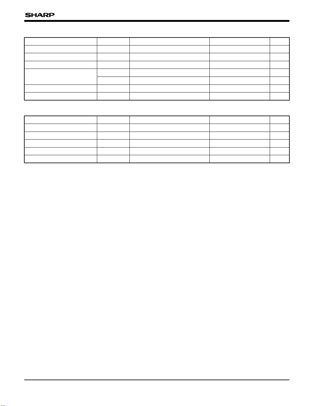
ABSOLUTE MAXIMUM RATINGS
PARAMETER SYMBOL CONDITION RATING UNIT
Supply voltage VDD – 0.3 to 6.5 V
Input voltage VI – 0.3 to VDD + 0.5 V
Output voltage VO – 0.3 to VDD + 0.5 V
Output current
IOH High-level output current 4 mA
IOL Low-level output current 4 mA
Operating temperature TOPR –10 to +60 ˚C
Store temperature TSTG –40 to +140 ˚C
RECOMMENDED OPERATING CONDITIONS
PARAMETER SYMBOL CONDITION RATING UNIT
Supply voltage VDD 4.5 to 5.5 V
System clock frequency fSYS VDD = 4.5 to 5.5 V 16.384 k to 5 M Hz
Maximum main clock frequency
fCK
VDD = 4.5 to 5.5 V 10 MHz
Subclock frequency fSUB VDD = 2.7 to 5.5 V 32.768 kHz
Operating temperature TOPR –10 to +60 ˚C
NOTE :
Be sure to RESETB when power on because internal signal reguires initialization. Normal operation is not guaranteed without
hardware reset.
- 7 -
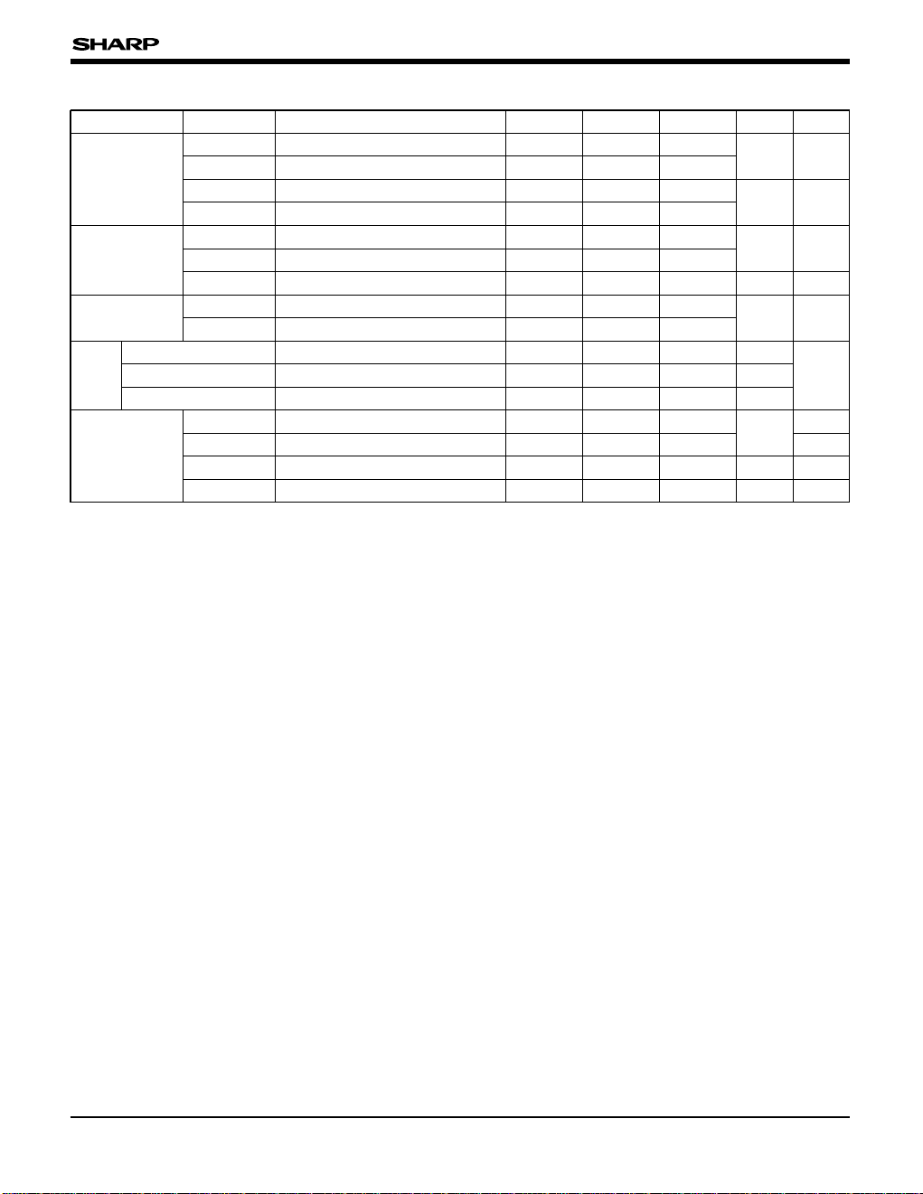
SM8521
NOTES :
1. Applicable pins : P00-P07, P10-P17, P20-P27, P30-P37, D0D7, VD0-VD7, X1, M0-M2
2. Applicable pins : RESETB, OSC1, RxDB, NMIB, INTB
3. Applicable pins : P0
0-P07, P10-P17, P20-P27, P30-P37,
VD0-VD7, X1, M0-M2 (non-connected
pull-up resistor)
4. Applicable pins : RESETB, P0
0-P07, P10-P17, P20-P27,
P3
0-P37 (connected pull-resistor)
5. Applicable pins : P0
0-P07, P10-P17, P20-P27, P30-P37, D0-
D7, A0-A20, MCE0B, MCE1B, IOE0B,
IOE1B, RDB, WRB, VA0-VA12, VCE0B,
VCE1B, VWRB, TxDB, XC, LP, FR,
CLK, XD0-XD3
6. No loadcondition, V
DD = 5 V, main clock = 10 MHz
7. No load condition, V
DD = 5 V, sub clock in active (32.768
kHz), VR = GND, input signal fixation.
8. No load condition, V
DD = 5 V, sub clock in active (32.768
kHz), VR = GND, input signal fixation.
Including LCD, DMA, sound generator and any part
concerned with timer operation.
9. No load condition, V
DD = 5 V, sub clock in active (32.768
kHz), VR = GND, input signal fixation.
10. No load condition, V
DD = 5 V, OSC1 = GND, VR = GND,
input signal fixation.
DC CHARACTERISTICS
PARAMETER SYMBOL
UNIT
NOTE
Input voltage
V
IH1 0.8 x VDD VDD
V 1
V
IH2 VDD – 0.5
0.5
10
V 2
VIL2
IIH1
µA
µA
3
4
IIL1 –10
IIL2 –40 –75 –150
0.5
8
10
± 0.10
45
18
70
6
± 0.05
30
15
30
1
Output voltage
VOH1 VDD – 0.5
V
bits
kΩ
V
mA
7
8
9
10
µA
µA
5
6
VOL1
D/A
Supply current
IDD
IDDH
IDDS1
IDDS2
MIN.
VIN = VDD, VDD = 5 V
VIH = 0 V, VDD = 5 V
VIN = 0 V, VDD = 5 V
IOH1 = –1 mA, VDD = 5 V
IOL1 = 10 mA, VDD = 5 V
VR = VDD = 5 V
VR = VDD = 5 V
VR = VDD = 5 V
fSYS = 5 MHz
fSYS = 5 MHz, HALT mode
fSUB oscillation, STOP mode
fSUB stop, STOP mode
MAX.TYP.
VIL1 0 0.2 x VDD
Input current
Resolution
Combined tolerance
Output resistance
(VDD = 4.5 to 5.5 V, TOPR = –10 to +60˚C)
CONDITION
- 8 -
SM8521
SM85CPU
The SM85CPU is an 8-bit CPU with an unique
architecture, developed by SHARP, and the
following features.
General purpose register architectures
• There are eight 8-bit general purpose registers
(also serve as four 16-bit general purpose
registers) and four 16-bit general purpose
registers serve as accumulator, index register, or
the pointer registers.
General purpose register allocated at RAM
• The general purpose registers access the RAM
location by the register pointer RP. So pushing
the register during an interrupt and passing
parameter to subroutine can be executed in High
speed.
Refined instruction set
• The instruction set contains total 67 members : 8
load instructions, 19 arithmetic instructions, 7 logic
instructions, 9 program control (branch) instruction,
8 bit manipulation instructions, 8 rotate & shift
instructions and 9 CPU control instructions.
• There are powerful bit manipulation instructions
includes plural bits transfer, logical operation
between bits, and the bit test and jump instructions
that incorporates a test and condition branch in the
same instruction. (Refer to Table 1)
• There are data transfer, arithmetic and conditional
branch instructions for 16-bit. It can rapidly
process the word-sized and long jump.
• There are 8-bit x 8-bit
→16-bit multiplication and
16-bit x 16-bit→16-bit remaining 8-bit division
instructions. (Unsigned arithmetic)
23 address modes
• The rich address modes provides optimal access
to ROM, RAM and the register files.
Illegal instruction detecting function
• When an error code is detected, a non-maskable
interrupt (NMI) will be generated.
Standby function
• There are two standby modes, HALT and STOP
mode, and the mode can be changed by HALT
instruction or STOP instruction respectively.
Table 1 Instruction summary
TYPE INSTRUCTION NUMBER
Load instruction CLR, MOV, MOVM, MOVW, POP, POPW, PUSH, PUSHW 8
Arithmetic instruction
ADC, ADCW, ADD, ADDW, CMP, CMPW, DA, DEC, DECW, DIV,
EXTS, INC, INCW, MULT, NEG, SBC, SBCW, SUB, SUBW
19
Logic instruction AND, ANDW, COM, OR, ORW, XOR, XORW 7
Program control instruction BBC, BBS, BR, CALL, CALS, DBNZ, IRET, JMP, RET 9
Bit manipulation instruction BAND, BCLR, BCMP, BMOV, BOR, BTST, BSET, BXOR 8
Rotate & shift instruction RL, RLC, RR, RRC, SLL, SRA, SRL, SWAP 8
CPU control instruction COMC, CLRC, DI, EI, HALT, NOP, SETC, STOP 8
Total 67
SM8521
- 9 -
Table 2 Addressing Mode Summary
NAME SYMBOL Range
Operand
∗
1
Implied
To specify the carry(C) and interrupt enable
(I) in the instruction code.
Register r r = R0-R7 General register [byte]
Register pair rr r = RR0, RR2, … , RR14 General register [word]
Register file R R = 0 to 255 (R0-R15)
Register file (0000H-007FH) and (0080H-00FFH)
[byte]
Register file pair RR
R = 0, 2, … 254
(RR0, RR2, … , RR14)
Register file (0000H-007FH) and (0080H-00FFH)
[byte]
Register indirect @r r = R0-R7 Memory (0000H-00FFH) [byte]
Register indirect
auto increment
(r)+ r = R0-R7 Memory (0000H-00FFH) [byte]
Register indirect
auto decrement
–(r) r = R0-R7 Memory (0000H-00FFH) [byte]
Register index
n(r)
∗
2
n = 00H-FFH, r = R1-R7 Memory (0000H-00FFH) [byte]
Register pair indirect @rr rr = RR0, RR2, … , RR14 Memory (0000H-FFFFH) [word/byte]
Register pair indirect
auto increment
(rr)+ rr = RR0, RR2, … , RR14 Memory (0000H-FFFFH) [word/byte]
Register pair indirect
auto decrement
–(rr) rr = RR0, RR2, … , RR14 Memory (0000H-FFFFH) [word/byte]
Register pair index
nn(rr)
∗
3
nn = 0000H-FFFFH
rr = RR2, RR4, … , RR14
Memory (0000H-FFFFH) [word/byte]
Index indirect
@nn(r)
∗
2
nn = 0000H-FFFFH
r = R1-R7
Memory (0000H-FFFFH) [word]
Immediate IM IM = 00H-FFH
The immediate data in the instruction code [byte]
Immediate long IML IML = 0000H-FFFFH
The immediate data in the instruction code [word]
Bit b b = 0 to 7
Register file (0000H-007FH) and memory
(0080H-00FFH, FF00H-FFFFH) [bit] (1bit of 1 byte
pointed by R, n(r) and DAp)
Port p Register file (0010H-0017H) [byte]
Relative RA PC – 128 to PC + 127 Program memory (1000H-FFFFH)
Direct DA DA = 0000H-FFFFH Memory (0000H-FFFFH) [byte]
Direct short DAs DAs = 1000H-1FFFH Program memory (1000H-1FFFH)
Direct special page DAp DAp = FF00H-FFFFH Program memory (FF00H-FFFFH) [byte]
Direct indirect @DA
DA = 0000H-FFFFH
Memory (0000H-FFFFH)
∗
1 The data indicated by [ ] is the unit of possible to use in Load and Arithmetic Instructions.
∗
2 R0 can not be used.
∗
3 RR0 can not be used.
SM8521
- 10 -
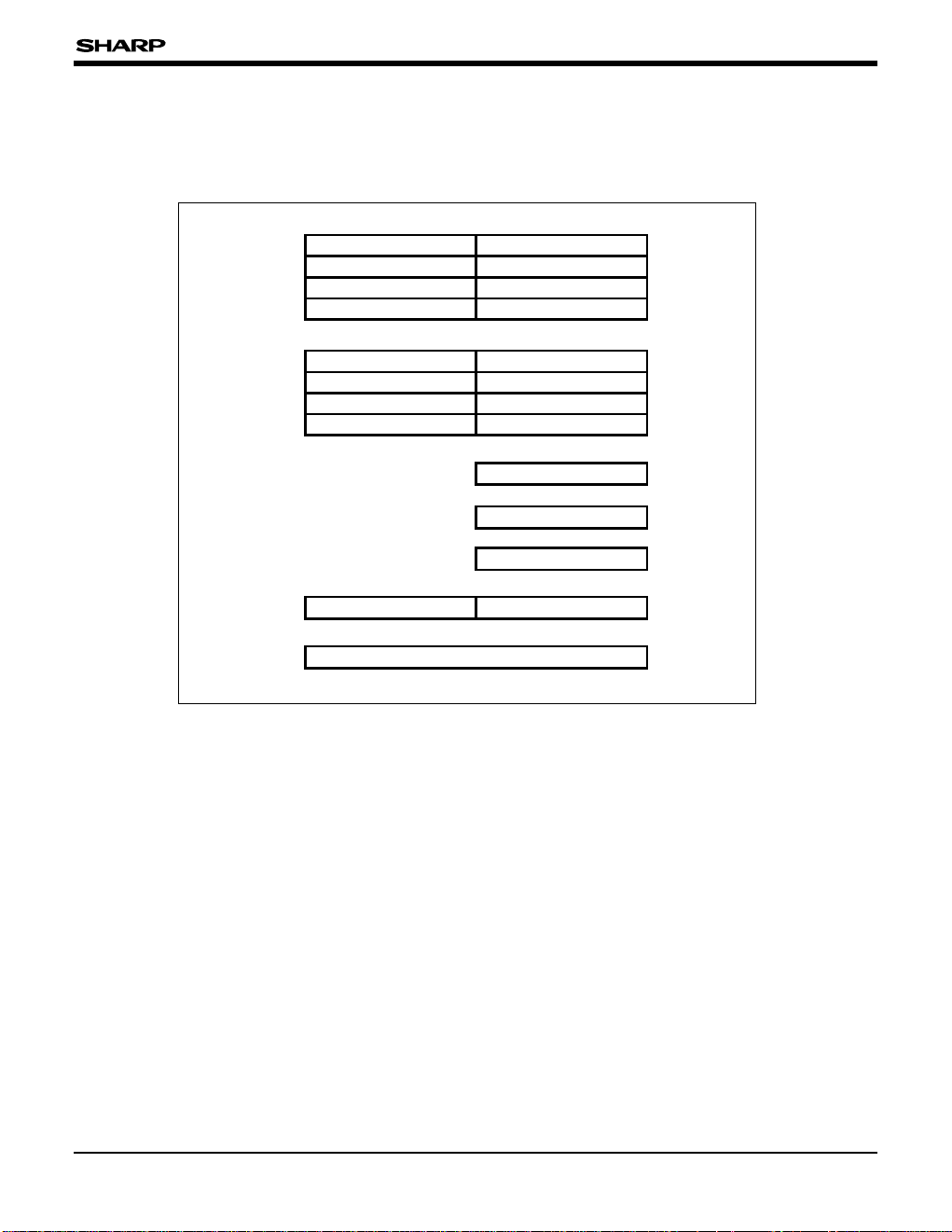
Register Lineup
Fig. 1 shows the SM85CPU register lineup. The CPU
internal register consists of eight 8-bit general purpose
registers (R0-R7), four 16-bit general purpose registers
(RR8-RR14), a program counter (PC) and four other
control registers. (The R0-R7 can be also used as
four 16-bit general purpose registers (RR8-RR14).)
GENERAL PURPOSE REGISTER
The eight 8-bit
general purpose registers
R0-R7 and
all eight 16-bit general purpose registers (RR0RR14) are available for use as accumulator, index
register and pointer registers. (The R0 and RR0
cannot be used as index register)
The other eight 8-bit registers R8-R15 cannot be used
as 8-bit general purpose register and as member of
the register file. (about register file, refer to "Address
Space.")
The feature of the SM85CPU architecture is that
general purpose registers
are virtually allocated at
16-byte internal RAM. Actually, if the CPU accesses
general purpose registers
, the designated RAM will
be accessed by the 5-bit register pointer (RP)
✽
.
When RP = 00000B, the registers occupy the first
16 bytes starting at 0000
H. Incrementing the field,
RP = 00001B, shifts the mapping by eight bytes so
that the registers start at 0008
H. As a result, the
general purpose registers
can be switched in 8-byte
unit to any RAM location within 0000
H-00FFH.
Although the
general purpose registers
are members
of the register file, which stores the data onto
actual RAM, is different from the other members
(control registers).
That is, general purpose registers can be referred as
registers, as register file (allocated at 0000
H
-000FH)
and as RAM accessing by all addressing modes.
∗ About register pointer (RP), refer to "Processor status 0
(PS0)".
RR0
RR2
RR4
RR6
R8
R10
R12
R14
RR8
RR10
RR12
RR14
R0
R2
R4
R6
7
15
07 0
R1
R3
R5
R7
R9
R11
R13
R15
0
70
70
70
7070
0
15
PS0
PS1
SYS
SPLSPH
PC
Fig. 1 Register Lineup
SM8521
- 11 -
CPU CONTROL REGISTER
The SM85CPU has the following control register :
processor status PS0, processor status PS1,
system configuration register SYS, stack pointer
SPH, SPL and program counter PC. All control
register except the program counter PC are
members of the register file and accessible by the
register file R and the register file pair RR
addressing modes.
Processor status 0 (PS0)
The processor status PS0 is an 8-bit readable/
writable register containing 2 fields, the upper 5-bit
is register pointer (RP) and the lower 3-bit is
interrupt mask.
Bit 7 0
Bits 7 to 3 : Register pointer (RP)
This gives, in 8 bytes unit, the starting address
in RAM for
general purpose registers
.
Bits 2 to 0 : Interrupt mask bits (IM)
Internal RAM
Address
R0
R1
R14
R15
High
Low
RP IMPS0
Ex.)
If RP=00000B, general purpose
registers will be virtually allocated
at internal RAM 0000H-000FH.
If RP=00001B, general purpose
registers will be virtually allocated
at internal RAM 0008H-0017H.
Fig. 2 Register Pointer (RP) Setting Example
BIT CONTENT
000
All maskable interrupts recognized
001
010
Maskable interrupts with level 1 to 12 recognized
011
Maskable interrupts with level 1 to 10 recognized
100
Maskable interrupts with level 1 to 8 recognized
101
Maskable interrupts with level 1 to 6 recognized
111
Maskable interrupts with level 1 tto 4 recognized
111
Maskable interrupts with level 1 to 2 recognized
PR4 PR3 PR2 PR1 PR0 IM2 IM1 IM0
- 12 -
SM8521
Processor status 1 (PS1)
The processor status PS1 is an 8-bit readable/
writable register and consists of eight flag bits.
These flags can be used as the condition codes for
the conditional branch instructions. When CPU
generates an interrupt, the content of processor
status PS1 and the value of program counter PC
automatically are pushed onto stack.
Bit 7 0
Bit 7 : Carry (C)
It indicates that generated a carry in operation.
Bit 6 : Zero (Z)
It indicates that the operation result is zero.
Bit 5 : Sign (S)
It indicates that the operation result is negative
(Sign bit = ‘1’).
Bit 4 : Overflow (V)
Executes the operation with the signed value. If
the operation result cannot indicate complement
on two, then the bit will be ‘1’.
Bit 3 : Decimal adjustment (D)
It indicates that the last arithmetic operation is a
subtraction.
Bit 2 : Half carry (H)
It indicates that generated a carry between bit 3
and 4.
Bit 1 : Bit (B)
It indicates that the result of the last bit
manipulation.
Bit 0 : Interrupt enable (I)
This is a flag which enables/disables all
maskable interrupt.
System configuration register (SYS)
The system configuration register SYS is an 8-bit
readable/writable register which sets the external
memory expansion modes and selects 8-bit/16-bit
stack pointer.
Bit 7 0
Bit 7 : Sets '0'
Bit 6 : Stack pointer configuration (SPC)
Bits 5 to 3 : Set '0'
Bits 2 to 0 : Memory configuration (MCNF2-0)
∗ : In ROM space (60 k bytes), the field beyond the internal
ROM is the external memory access field.
Stack pointer (SPL, SPH)
The stack pointer SPL, SPH are 8-bit readable/
writable register and show the stack address. The
bit SPC of the system configuration (SYS) specifies
whether the stack pointer is 8 (SPL only) or 16
(both SPL and SPH) bits long.
Program counter (PC)
The program counter (PC) is a pointer for program
memory and contains the starting address for the
next instruction.
The program counter PC is initialized to 1020
H after
hardware reset. That is, the application program
starts executing from the address 1020
H after
hardware reset.
0
BIT
8-bit (SPL only)
CONTENT
1 16-bit (both SPL, SPH)
- SPC - - -
MCNF2 MCNF1 MCNF0
CZSVDHBI
BIT CONTENT
000 External memory expansion disable.
110
External memory expansion mode
(64 k bytes✽)
Other
combination
Do not use.
Bit 15 0
SM8521
- 13 -
76543210
MSB LSB
MSB
Upper 8-bit
LSB
Lower 8-bit
Address
High
Low
Data Format
0000
H-00FFH
0000H-00FFH
Even byte, 0000H-00FEH,
following byte (odd byte)
0000H-00FFH
Register file address
Bit
Byte
Word
BCD
Data
Type
70
Upper BCD digit Lower BCD digit
0000H-00FFH or FF00H-FFFFH
0000H-00FFH
0000H-00FFH or FF00H-FFFFH
(Under shorthand)
0000
H-FFFEH
following byte
0000
H-00FFH
Memory address
Fig. 3 Register File/Memory Data Formats
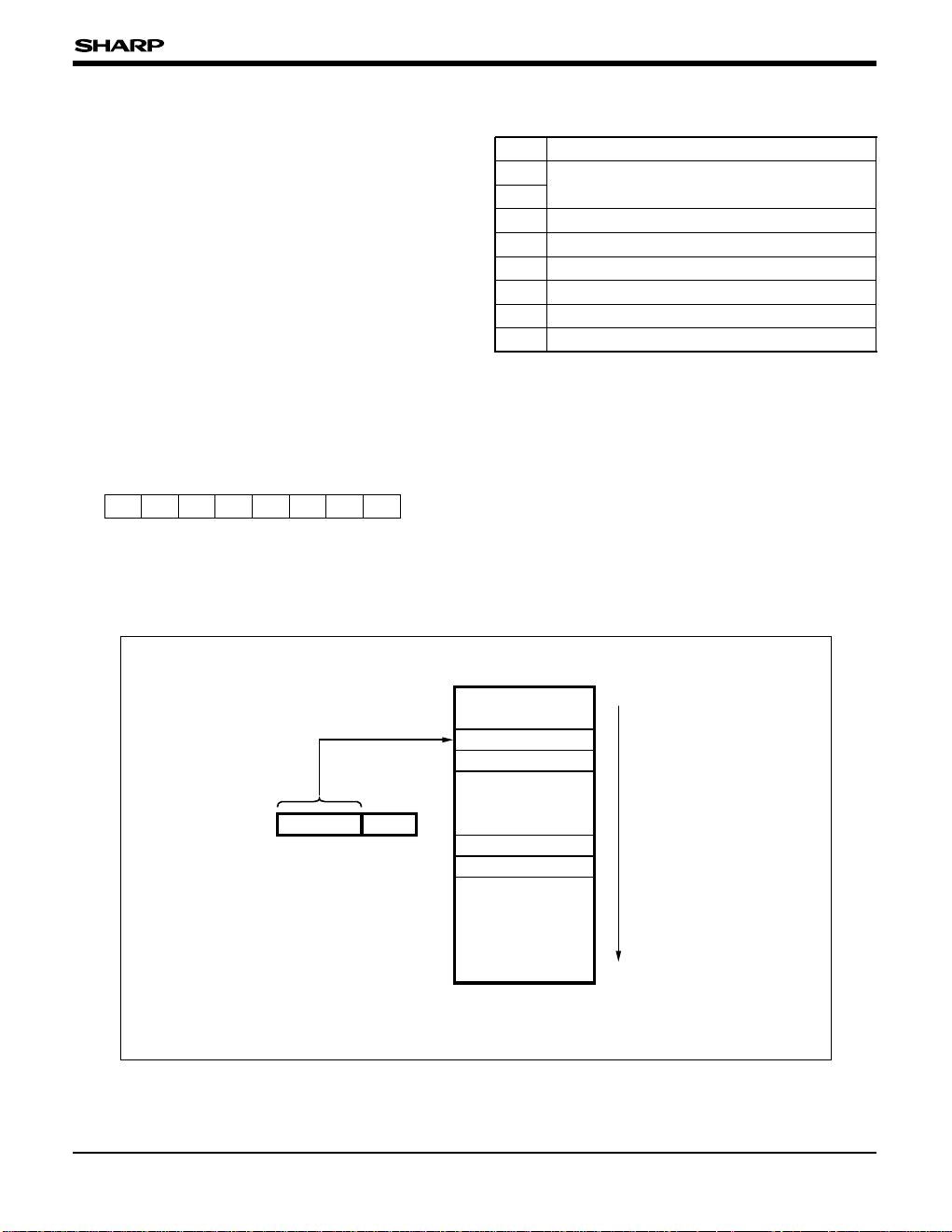
Address Space
The SM85CPU has a 64 k-byte address space,
which is divided into RAM (0000
H-0FFFH) and ROM
(1000
H-FFFFH) areas. The address 0000H-007FH
are both shared by RAM and register file. Fig. 9-1
shows the SM8521 Memory Map.
The RAM and register file allocated at 0000
H-007FH
can be selected by the addressing mode
designated by instructions.
The SM8521 supports an Memory Management
Unit used to external memory area expantion.
Refer to "Memory Management Unit (MMU)".
ROM Area
ROM area starts at the address 1000H of the space
address. The first portion (1000
H-101FH) is reserved
for the interrupt vector table. Each 2 bytes entry in
the vector table contains the address of interrupts.
When an interrupt encountered, the CPU jumps to
the corresponding branch address of vector table
for program executing. The address 1020
H marks
the start of the user program area itself. Executing
always starts at 1020
H after hardware reset.
Register File Area
The register file is allocated between 0000H and
007F
H. The first 16 bytes (0000H-000FH) area are
general registers. The remainder is for CPU control
registers, peripherals control register and data
register.
RAM Area
The RAM area starts at the beginning 0000H of the
address space. It overlaps the register file for the
address 0000
H-007FH.
This arrangement is to shorten the instruction
length as much as possible and to permit the use
with both RAM and the register file for faster
execution.

- 14 -
SM8521
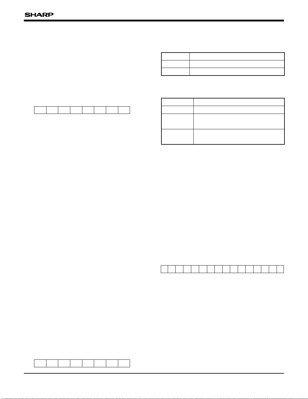
Data Format
The SM85CPU supports four data types : bit, 4-bit
BCD, byte, and word data.
REGISTER FILE DATA FORMATS
The register file (0000H-007FH) and RAM (0080H-
00FF
H) accessible with register file R and register
file pair RR addressing support processing for all 4
data types : bit, 4-bit BCD, byte, and word data.
Fig. 3 shows the data layout in the register file.
• Bit data (register file)
Bit manipulation instructions access bit data in the
register by register file R addressing, which gives
the byte address in the register file (0000
H-007FH),
or RAM (0080
H-00FFH), and the operand b, which
gives the bit number within the byte.
• Byte data (register file)
Instructions access the byte data in the register file
by register file R addressing, which gives the byte
data address in the register file (0000
H-007FH) or
RAM (0080
H-00FFH).
• Word data (register file)
Instructions access word data in the register file by
register file pair RR addressing, which gives the word
address, even and 2 bytes address, in the register
file (0000
H-007FH) or RAM (0080H-00FFH). The
address must be even (0, 2, 4,…, 254). Specifying an
odd address leads to unreliable results.
• BCD data (register file)
The decimal adjust instruction (DA), used to adjust
BCD digits after an odd or subtraction, accesses a
BCD data byte in the register file by register file R
addressing.
•
Notice for the general register on register file
The general registers are the first 16 bytes (0000H-
000F
H) in the register file. They can be accessed
as byte-sized by register file R addressing and as
word-sized by register file pair RR addressing.
MEMORY DATA FORMATS
The memory area (ROM and RAM 0000H-FFFFH)
supports processing for all 4 data types : bit, 4-bit
BCD, byte and word data. However, bit data is
limited to the ranges (0000
H-00FFH, FF00H-FFFFH),
and 4-bit BCD data to the ranges 0000
H-00FFH.
Fig. 3 shows the data layout in memory.
• Bit data (memory)
Bit manipulation instructions access bit data in
memory by register index n(r) addressing, which
gives the byte address in the range (0000
H-00FFH),
or by direct special page DAp addressing, which
gives the byte address in the range (FF00
H-FFFFH),
and the operand b, which gives the bit number
within the byte.
• Byte data (memory)
Instructions access the byte data in memory by
shorthand (0000
H-00FFH or FF00H-FFFFH) or full
(0000
H-FFFFH) address.
• Word data (memory)
Instructions access the word data, continue 2
bytes, in memory by shorthand (0000
H-00FFH or
FF00
H-FFFFH) or full (0000H-FFFFH) address.
Unlike word data in the register file, the address
can be even or odd.
• BCD data (memory)
The decimal adjust instruction (DA), used to adjust
BCD digits after an odd or subtraction, accesses a
BCD data byte in memory by register index @r
addressing.
• Notice for general register on memory
The general registers are actually in a RAM area
specified by register pointer RP, so they can be
read and modify directly as RAM. While
programming, the programmer must take care to
arrange program data so that other RAM
operations do not destroy general registers content.
SM8521
- 15 -
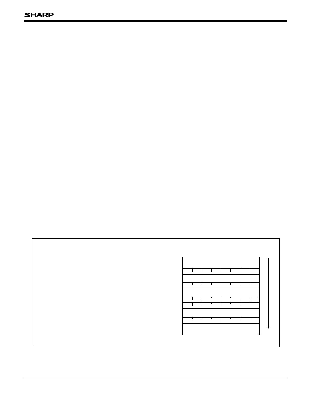
Bus Timing
The SM85CPU is variable for system clock. The bit
FCPUS2-FCPUS0 (bits 5 to 3 : CKKC) of the clock
changing register CKKC can select system clock to
1/2, 1/4, 1/8, 1/16 and 1/32 of the main clock and
1/2 of sub-clock. The CPU operates at 1/32 clock
of the main clock after hardware reset.
INTERNAL MEMORY ACCESS TIMING
The read cycle of internal RAM is 2 cycles. The
internal RAM supports 2 cycles for reading or
writing.
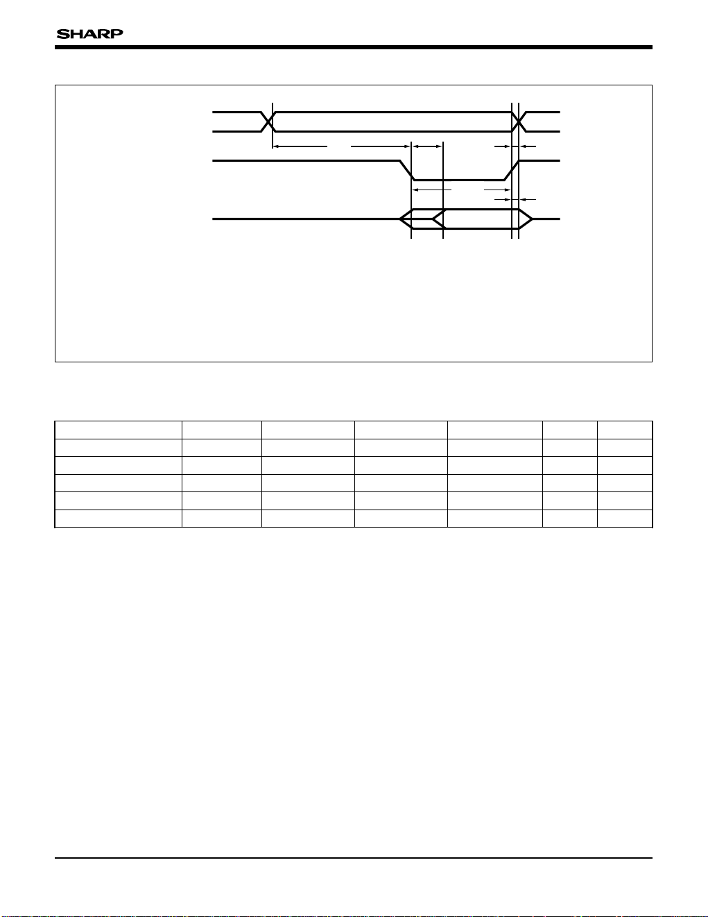
EXTERNAL MEMORY ACCESS TIMING
The external memory supports 2 cycles for reading
or writing. Fig. 5 shows the read timing and Fig. 6
shows the write timing.
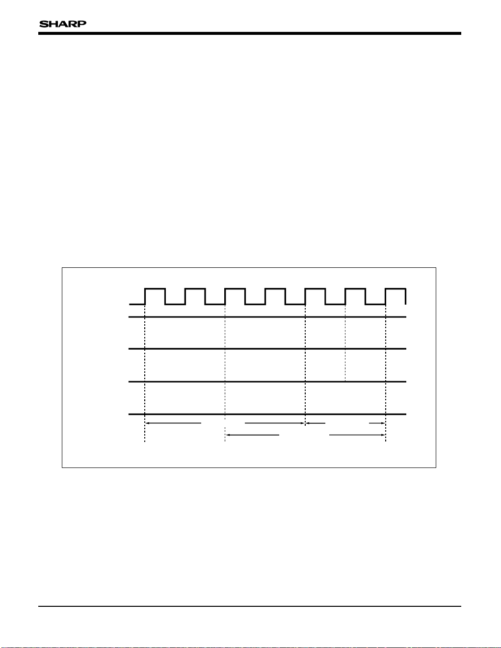
INSTRUCTION PREFETCH
The SM85CPU, which execution cycle overlaps
with the OP code, fetches next instruction OP
code during one instruction execution cycle. For
example, the execution time for 2 bytes instructions
(MOV R, r) of transferring the RAM contents to a
register is 4 cycles.
Internal clock
Pre-instruction
Transfer
instruction
Next instruction
Fetch cycle
Execution
cycle
Executing
preinstruction
OP code
fetch
Operand
fetch
RAM
read
Register
write
OP code
fetch
Execution time
Fig. 4 Instruction Execution for Transfer Instruction (2 Bytes)
SM8521
- 16 -
RDB
Valid data
D0-D7
t
RHD
t
RHA
t
RSA
t
RSD
t
WRD
A0-A
20
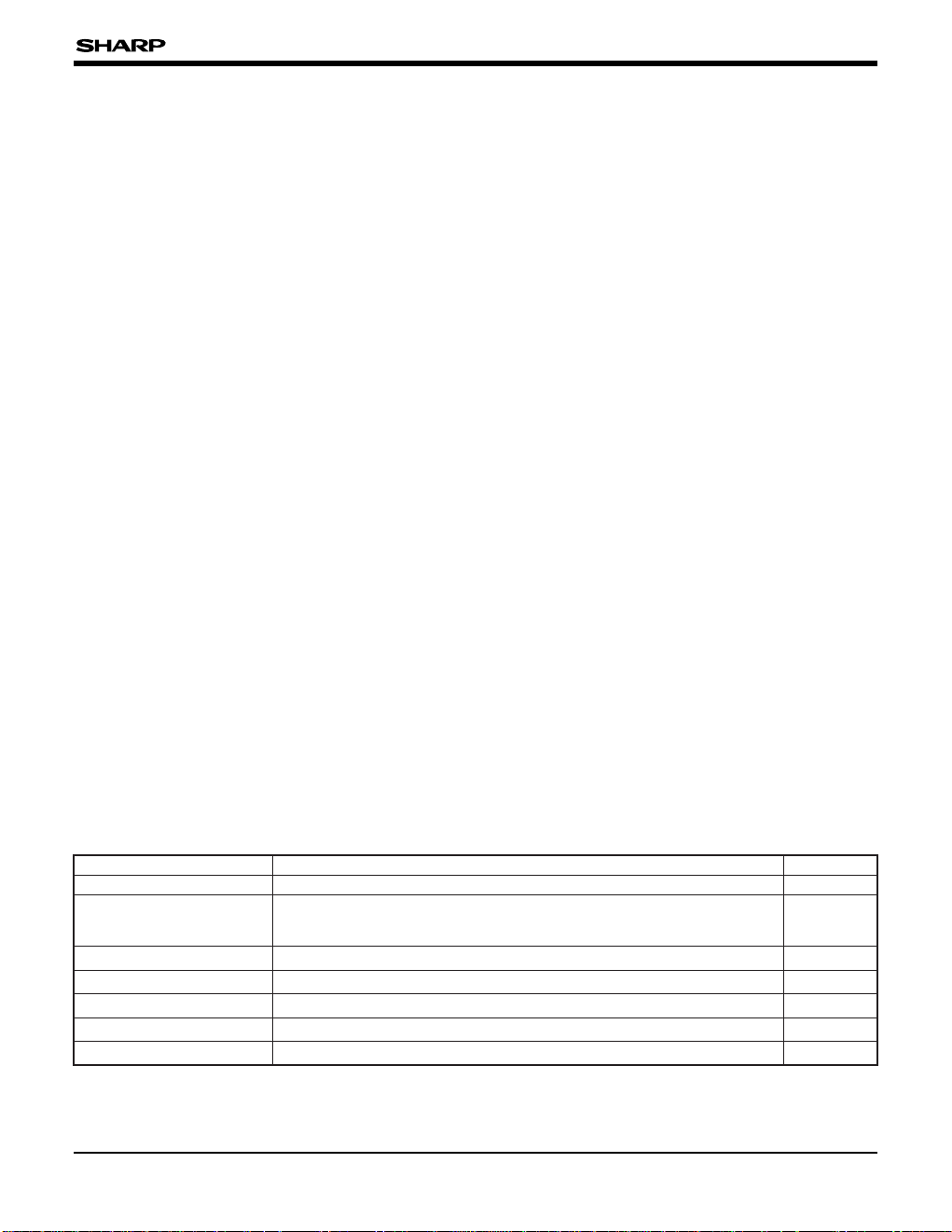
• External memory access timing (read timing)
Operating condition (VDD = 4.5 to 5.5 V, TOPR = –10 to 60˚C)
PARAMETER SYMBOL UNIT
NOTE
Address setup time tRSA tSYS tSYS + 50 ns 1
Read data setup time tRSD tSYS/2 – 30 ns 1
RDB signal pulse width
tWRD tSYS – 50 tSYS ns 1
Address hold time tRHA 0 ns
Read data hold time tRHD 0 ns
MIN. TYP. MAX.
NOTE :
1. tSYS : The system clock period (main clock x 1/2) when the
low order 3 bits in the clock change register
FCPUS2-FCPUS0 are 100
B.
tRSA : The time between address firm and RDB signal
falling Low level firm.
t
RSD : The time between RDB signal firm and input valid
data firm.
t
WRD : RDB signal Low level width.
t
RHA : The time between RDB signal rising High level firm
and address change.
t
RHD : The time between RDB signal rising High level firm
and output data floating.
Load capacitance is 50 pF.
Fig. 5 External Memory Access Timing (Read Timing)
SM8521
- 17 -
WRB
D
0
-D7
Valid data
t
WSA
Invalid data
t
WSD
t
WHD
t
WHA
t
WWR
A0-A
20
• External memory access timing (write timing)
Operating condition (VDD = 4.5 to 5.5 V, TOPR = –10 to 60˚C)
PARAMETER SYMBOL UNIT NOTE
Address setup time tWSA
tSYS
tSYS + 50
ns
1
Data setup time tWSD tSYS – 50 tSYS + 30
ns
1
WRB signal pulse width
tWWR tSYS – 60
tSYS ns
1
Address hold time tWHA 10
ns
Data hold time tWHD 10
ns
MIN. TYP. MAX.
NOTE :
1. tSYS : The system clock period (main clock x 1/2) when the
low order 3 bits in the clock change register
FCPUS2-FCPUS0 are 100
B.
t
WSA : The time between address firm and WRB signal
falling Low level firm.
t
WSD : The time between WRB signal rising High level firm
and output valid data firm.
t
WWR : WRB signal Low level width.
t
WHA : The time between WRB signal rising High level firm
and address change.
t
WHD : The time between WRB signal rising High level firm
and output data floating.
Load capacitance is 50 pF.
Fig. 6 External Memory Access Timing (Write Timing)
 Loading...