

Sharp PC902 Datasheet

PC902
PC902
AC Input Type OPIC
Photocoupler
■ Features
1. Capable of forming an integration circuit
in conjunction with an external capacitor
2. AC input
3. High sensitivity
(I
: MAX. 2mA
FHL
)
4. High isolation voltage between input and
output
(V
: 5 000V
iso
)
rms
5. Standard dual-in-line package
6. Recognized by UL, file No. E64380
■ Applications
1. Programmable controllers
2. Telephone sets
3. AC line monitors
■ Outline Dimensions
± 0.5
1 NC
2 V
3 V
4 NC
1.2
IN1
IN2
± 0.3
5678
2.54
TYP.
0.5
± 0.3
0.85
PC902
1234
Primarys side mark (Sunken place
9.22
± 0.5
3.5
± 0.5
3.0
0.5
± 0.1
± 0.5
6.5
± 0.25
diagram
10k Ω
Voltage
regulator
1234
)
θ
5 V
AUX
6 GND
7 V
O
8 V
CC
(
Unit : mm
Internal connection
0.01µ F
(
ExternalC
65
78
± 0.3
7.62
θ
= 0˚ to 13˚
± 0.1
0.26
)
)
Amp
θ
* “OPIC ” (Optical IC) is a trademark of the SHARP Corporation.
An OPIC consists of a light-detecting element and signal processing circuit integrated onto a single chip.
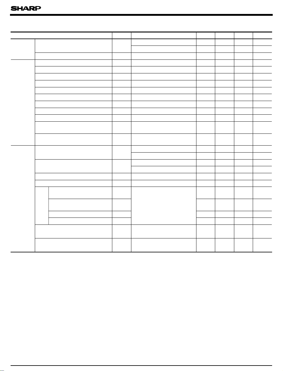
■ Absolute Maximum Ratings
(
Ta= 25˚C
)
Parameter Symbol Rating Unit
Input
Forward current I
*1
Peak forward current I
F
FM
±20 mA
±1 A
Power dissipation P 30 mW
Supply voltage V
Output
Output voltage V
Output current I
Power dissipation P
Total power dissipation
*2
Isolation voltage
Operating temperature T
Storage temperature T
*3
Soldering temperature T
“ In the absence of confirmation by device specification sheets, SHARP takes no responsibility for any defects that occur in equipment using any of SHARP's devices, shown in catalogs,
data books, etc. Contact SHARP in order to obtain the latest version of the device specification sheets before using any SHARP's device. ”
CC
O
O
O
P
tot
V
iso
opr
stg
sol
15 V
15 V
16 mA
150 mW
170 mW
5 000
V
- 25 to + 85 ˚C
- 55 to + 125 ˚C
260 ˚C
rms
*1 Pulse width<=100 µs,
Duty ratio : 0.001
*2 40 to 60%RH, AC for
1 minute
*3 For 10 seconds
PC902
■ Electro-optical Characteristics
Parameter
Input
Output
Transfer
charac-
teristics
Forward voltage V
Terminal capacitance C
Operating supply voltage V
Low level output voltage V
High level output voltage V
Low level supply current I
High level supply current I
AUX source current I
AUX sink current I
AUX terminal voltage 1 V
AUX terminal voltage 2 V
“ High→Low” threshold
AUX voltage
“ Low→High” threshold
AUX voltage
“ High→Low” threshold
input current 1
“ High→Low” threshold
input current 2
Isolation resistance R
Floating capacitance C
“ High→Low ” propagation delay time
“ Low→High ” propagation delay time
time
Response
*4
*5
Instantaneous common
mode rejection voltage
“ Output : High level ”
*5
PInstantaneous common
mode rejection voltage
“ Output : Low level ”
(
Ta= 0 to + 70˚C unless otherwise specified
Symbol Conditions MIN. TYP. MAX. Unit
IF= ± 20mA - - 1.5 V
F
= ± 0.1mA 0.55 0.95 - V
I
F
CC
OLIOL
OH
CCLIF
CCH
AUX1
AUX2
AUX1
AUX2
V
AUXHL
V
AUXLH
I
FHL1
I
FHL2
ISO
t
PHL
PLH
f
r
CM
CM
V
= 0, f= 1kHz
t
F
= 8.0mA, VCC= 5V, IF= ± 2mA
VCC= 5V, IF= 0 3.5 - - V
= ± 2mA, VCC= 5V - 1.7 4.0 mA
VCC= 5V, IF= 0 - 1.5 3.5 mA
Ta = 25˚C, IF= ± 2mA, VCC= 5V, V
Ta = 25˚C, IF= 0, VCC= 5V, V
AUX
AUX
= 1.3V
= 1.3V
Ta= 25˚C, IF= 0, VCC= 5V - - 0.2 V
Ta= 25˚C, IF= ± 2mA, VCC=5V
Ta= 25˚C, IF= 0, VCC= 5V 2.05 - 2.55 V
Ta= 25˚C, IF= 0, VCC= 5V 0.75 - 1.10 V
Ta= 25˚C, VCC= 5V, RL= 680Ω
= 5V, RL= 680Ω 0.1 - 2.0 mA
V
CC
Ta= 25˚C, VCC= 5V, RL= 680Ω
= 5V, RL= 680Ω - 0.1 - - 2.0 mA
V
CC
Ta= 25˚C, DC500V, 40 to 60% RH
Ta= 25˚C, V = 0, f= 1MHz - 0.6 5 pF
f
Ta= 25˚C
= ± 2mA, VCC=5V
I
F
= 0.01 µ F
C
AUX
= 680Ω
R
L
Ta = 25˚C, IF= 0, VCM= 600V (peak
H
V
= 2V, RL= 680 Ω, C
)
O(MIN.
Ta = 25˚C, IF= ± 2mA, V
L
V
= 0.8V, RL= 680 Ω, C
)
O(MAX.
AUX
= 600V (peak
CM
AUX
)
= 0.01 µ F
)
= 0.01 µ F
- 30 250 pF
4.5 - V
15
- 0.1 0.4 V
-2 -3 -5 µA
1.0 1.5 2.5 µ A
2.3 - 2.8 V
- 0.7 1.5 mA
- - 0.7 - 1.5 mA
5x101010
11
- Ω
4.5 7.0 10 ms
6.5 10.5 15 mst
- 0.05 0.5 µ sFall time t
- 0.1 0.5 µ sRise time t
--V/µs
2 000
--V/µs
- 2 000
)
 Loading...