

Sharp LH5316P00BN Datasheet
LH5316P00B
CMOS 16M (2M × 8/1M × 16) MROM
FEATURES
•• 2,097,152 × 8 bi t organ izatio n
(Byte mode: BYTE = VIL)
1,048,5 76 × 16 bit orga nization
(Word mode: BYTE = VIH)
•• Access time: 120 ns (MAX.)
•• Supply curre nt :
– Operating: 70 mA (MAX.)
– Standby: 100 µA (MAX.)
•• TTL compatible I/O
•• Three-state output
•• Singl e +5 V p owe r su ppl y
•• Static operation
•• Package:
44-pi n , 600 -mil S OP
•• Item related with COCOM regulation :
– Non programmab le
– Not de sign ed o r rate d as rad iatio n
hardene d
– CMOS process (P typ e sil icon
substrate)
DESCRIPTION
The LH5316P00B is a 16M-bit mask-programmable
ROM organized a s 2 ,097,152 × 8 bits (Byte mode) or
1,048,576 × 16 bits (Word mode) that can be selected
by a BYTE input pin. It is fabricated using silicon-gate
CMOS process technology.
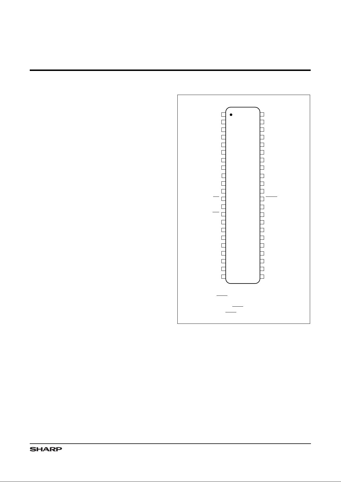
PIN CONNECTIONS
5316P00B-1
TOP VIEW
5
6
7
8
11
12
34
33
32
31
30
29
26
9
10
28
27
A
15
A
16
BYTE
13
14
15
36
35
A
13
16
25
D15/A
-1
(NOTE)
D
13
D
5
D
6
A
14
44-PIN SOP
3
4
38
37
1
2
4039A
10
D
14
D
7
24
23
V
CC
D
4
D
12
17
18
19
20
A
9
A
11
A
12
41
A
8
A
19
NC
42
21
OE
A
1
A
0
GND
CE
A
2
D
8
D
9
A
3
A
4
A
5
A
6
D
1
A
7
D
2
D
3
D
10
A
17
A
18
D
0
GND
D1122
NC
43
44
NOTE: The D15/A-1 pin becomes LSB address input (A-1)
when the BYTE pin is set to be LOW in byte mode and
data output (D
15
) when set to be HIGH in word mode.
The input state of BYTE pin can not be changed during
operation. The BYTE pin must be set to either GND or VCC.
Figure 1. Pin Connecti ons
1
5316P00B-2
A
4
A
3
A
13
A
12
A
11
A
10
A
9
37
38
39
40
4
7
8
A
8
A
7
A
5
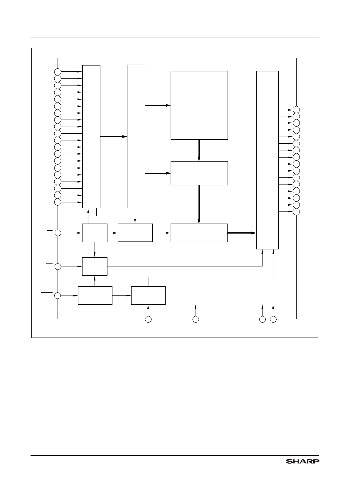
MEMORY
MATRIX
(2,097,152 x 8)
(1,048,576 x 16)
SENSE AMPLIFIER
42
33
6
A
1
A
0
10
11
A
2
9
41
A
6
5
A
14
36
ADDRESS BUFFER
CE
ADDRESS DECODER
COLUMN SELECTOR
CE
BUFFER
OE
BUFFER
A
15
35
A
16
34
12
TIMING
GENERATOR
A
17
3
BYTE
A
18
2
A
19
43
ADDRESS
BUFFER
BYTE/WORD
SWITCHOVER
CIRCUIT
14
OE
DATA SELECTOR/OUTPUT BUFFER
D
3
D
2
D
1
D
12
D
11
D
10
D
9
D
8
D
7
D
6
D
4
D
5
D
13
D
0
D
14
D
15
22
20
18
16
26
19
17
15
21
30
24
25
27
29
31
28
31
A
-1
V
CC
23
GND
13 32
Figure 2. LH5316P00B Block Diagram
PIN DESCRIPTION
SIGNA L PIN NAME
A
-1
- A
19
Addr ess in put
D
0
- D
15
Data ou tput
BYTE
×8bit / ×16 bit
(Byt e/w ord) mo de
sele ct input
CE Chip en abl e in pu t
SIGNAL PIN NAME
OE Outpu t e nab le i np ut
V
CC
Power su ppl y
GND Groun d
NC No co nne cti on
LH5316P0 0B CMOS 1 6M (2M x 8 /1M x 16) MROM
2
 Loading...