

Sharp LH52258AK-25, LH52258AK-20, LH52258AD-20, LH52258AD-25 Datasheet
LH52258A
CMOS 32K × 8 Static RAM
FEATURES
•• Fast A ccess T imes: 20/25 ns
•• Low-Power Standby when Deselected
•• TTL Compatible I/O
•• 5 V ± 10% Supply
•• Fully-Static Operation
•• JEDEC Standard Pinout
•• Packages:
28-Pin, 300-mil DIP
28-Pin, 300-mil SOJ
FUNCTIONAL DESCRIPTION
The LH52258A is a high-speed 2 62,144 bit static RAM
organized as 32K × 8. A fast , ef ficien t des ign is obt ained
with a CMOS periphery and a matrix constructed with
polysilicon load memory cel ls.
This RAM is fully static in opera tion. The Chip Enable
(E) control permits Read and Write operations when
active (LOW) or places the RAM in a low-power standby
mode when inactive (HI GH). Standby power (I
SB1
) drops
to its lowest level if E is raised to within 0.2 V of VCC.
Write cycles occur when bo th Chip Enable (E) and
Write Enable (W) are LOW. Data is transferred from the
DQ pins to the memory location specified by the 15
address lines. The proper use of the Output Enable
control (G) can prevent bus contention.
When E is LOW and W is HIGH, a sta tic Read will
occur at the memory location specified by the address
lines. G must be brought LOW to enable the outputs.
Since the device is fully static in operation, new Read
cycles can be performed by simply changing the address .
High-frequency design techniques should be employed to obtain the best performance from this device.
Solid, low-impedance power and ground planes, with
high-frequency decoupling capacitors, are recommended. Serie s terminat ion of the inputs should be considered when tra nsmis sion l ine effect s occur .
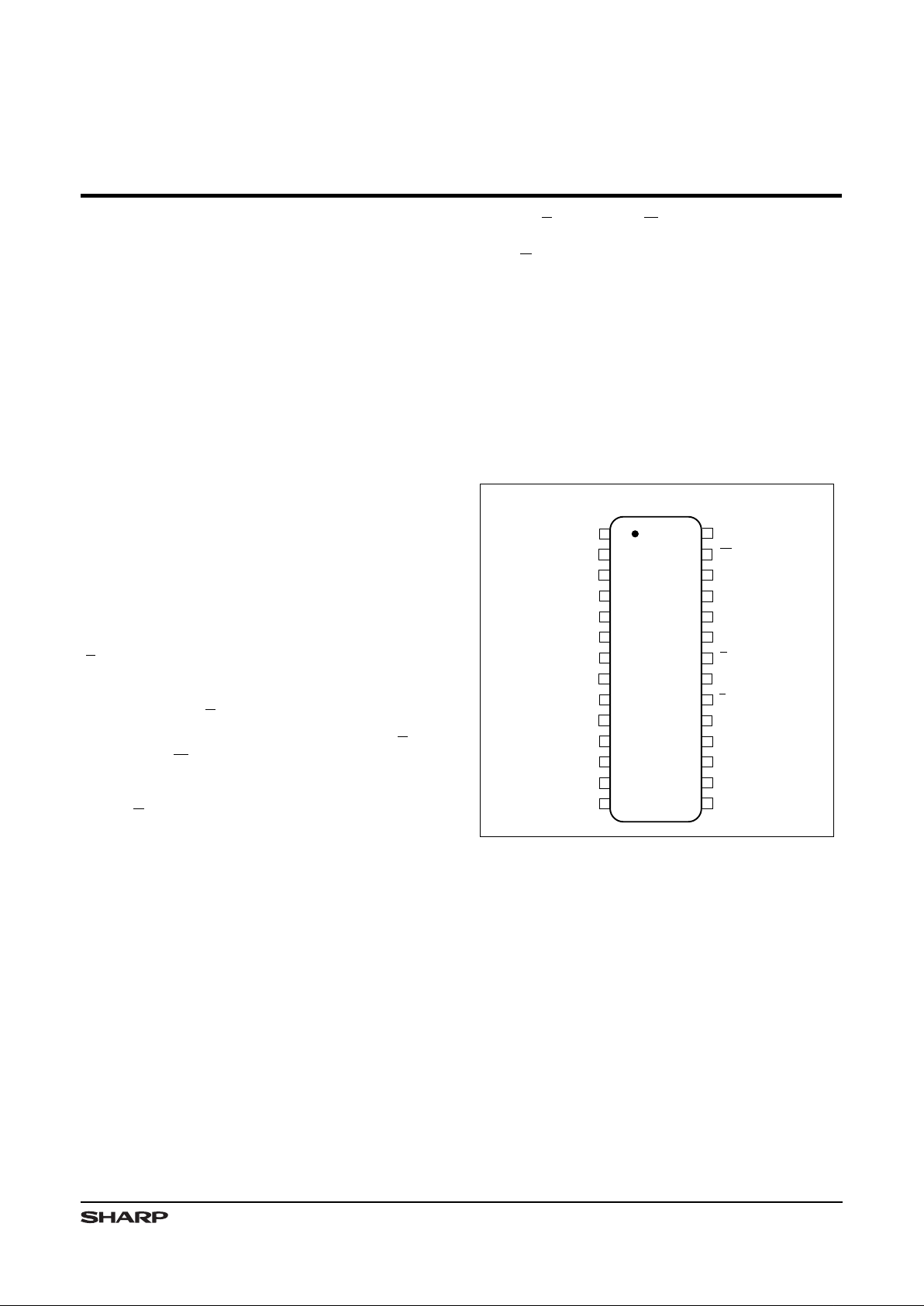
PIN CONNECTIONS
52258A-1D
1
2
3
4
5
6
7
8
9
10
11
12
A
14
A
12
A
7
A
6
A
5
A
4
A
3
A
2
A
1
A
0
V
SS
28
27
26
25
24
23
22
21
20
19
V
CC
W
A
8
A
9
A
11
G
A
10
DQ
7
DQ
6
DQ
5
18
17
DQ
3
13
14
16
15
DQ
0
DQ
4
A
13
DQ
1
DQ
2
E
28-PIN DIP
28-PIN SOJ
TOP VIEW
Figur e 1. Pin Connect ions for DIP and
SOJ Packages
1
TRUTH T ABL E
E G WMODE DQ I
CC
HXX
Not Selected High-Z Standby
LHH
Selected High-Z Active
LLH
Read Data Out Active
LXL
Write Data In Active
PIN DESCRIP TIONS
PIN DESCRIPT ION
A0 – A
14
Address Inputs
DQ0 – DQ
7
Data Input s/ Outp uts
E Chip Enable
G Output Enable
W Write Enable
V
CC
Positive Po wer Supply
V
SS
Ground
52258A-2
MEMORY ARRAY
(32,768 x 8)
I/O CIRCUIT
BLOCK
DECODE
COLUMN
DECODE
A0A
3
A
10
A11A9A8A
13
E
W
A
4
A
5
A
1
A
2
A
6
A
7
A
12
A
14
G
DQ0 - DQ
7
8
8
8
ROW DECODER
Figure 2. LH52258A Block Diagram
LH52258A CMOS 32 K × 8 Static RAM
2
ABSOLUT E MAXIMUM R ATI NGS
1
PARAMETER RATING
VCC to VSS Potential –0.5 V to 7 V
Inpu t Volt age R ange –0.5 V to VCC + 0.5 V
DC Outp ut C ur r en t
2
± 40 mA
Stor age Temper atu re Ran g e –65o to 150oC
Power Dissipat ion (Pac kage Lim it) 1.0 W
NOTES :
1. Stresses greater than those listed under ‘Absolute Maximum Ratings’ may cause permanent damage to the device. This is a stress rating for
transient conditions only. Functional operation o f the devic e at these or any other conditions above those indicated in the ‘Operating Range’
section of this specification is not implied. Exposure to absolute maximum rating conditions for extended periods may affect reliab ility.
2. Outputs should not be shorted for more than 30 seconds. No more than one output should be shorted at any time.
OPERATING RANGES
SYMBOL PARAMETER MIN TYP MAX UNIT
T
A
T em per at ur e, Ambie nt
070
o
C
V
CC
Supply Volt age
4.5 5.0 5.5 V
V
SS
Supply Volt age
00 0 V
VILLogic ‘0’ Input V olt age
1
–0.5 0.8 V
V
IH
Logic ‘1’ Input Volt age
2.2 VCC + 0.5 V
NOTE:
1. Negative undershoot of up to 3.0 V is permitted once per cycle.
DC ELECTRICAL CHARACTERISTICS
SYMBOL PARAMETER TEST CONDITIONS MIN TYP 1MAX UNIT
I
CC1
Opera ting Cur re nt
2
tRC = 20 ns
G ≥ VIH, E ≤ VIL, I
OUT
= 0 mA,
t
CYCLE
= 20 ns
95 150 mA
I
CC1
Opera ting Cur re nt
2
tRC = 25 ns
G ≥ VIH, E ≤ VIL, I
OUT
= 0 mA,
t
CYCLE
= 25 ns
90 140 mA
I
SB1
Standby Cur ren t
E ≥ VCC – 0.2 V 0.005 1 mA
I
SB2
Standby Cur ren t E ≥ V
IH
615mA
ILIInput Leakage Current VCC = 5 .5 V, VIN = 0 V to V
CC
–2 2
µA
I
LO
I/O Leakage Cu rrent VCC = 5 .5 V, VIN = 0 V to V
CC
–2 2
µA
V
OH
Output High Volta ge IOH = –4.0 mA
2.4 V
V
OL
Output Low Volt age IOL = 8 .0 m A
0.4 V
V
DR
Data Retention Voltage E ≥ VCC – 0.2 V
25.5V
IDRData Retention Current
VCC = 3 V, E ≥ VCC – 0.2 V 250
µA
NOTES:
1. Typical values at VCC = 5 V, TA = 25°C.
2. ICC is dependent upon output loading and cycle rates. Specified values are with outputs open, operating at specified cycle times.
CMOS 32K × 8 Static RAM LH52258A
3
 Loading...