

Page 1
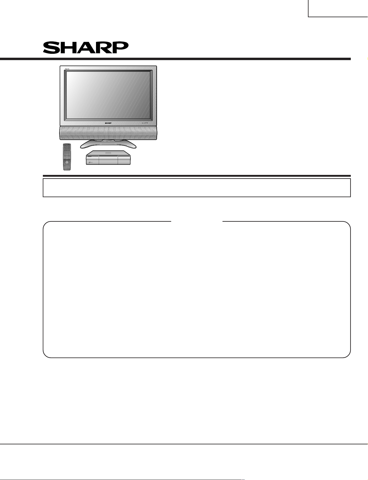
LC-37HV6U
SERVICE MANUAL
SY3M1LC37HV6U
LCD COLOR TELEVISION
MODEL
In the interests of user-safety (Required by safety regulations in some countries) the set should be restored to its original condition and only parts identical to those specified should be used.
LC-37HV6U
CONTENTS
Page
» IMPORTANT SERVICE SAFETY PRECA UTION .....2
» SPECIFICATIONS................................................ 5
» OPERATION MANUAL ........................................ 6
» DIMENSIONS ....................................................13
» REMOVING OF MAJOR PARTS........................15
»
ADJUSTMENT PROCEDURES (AVC System) ..
» UPGRADING INSTALLED PROGRAMS ...........34
» ADJUSTMENT PROCEDURES (Display) .........37
» TROUBLE SHOOTING TABLE ..........................43
» MAJOR IC INFORMATIONS (AVC System) ...... 54
» MAJOR IC INFORMATIONS (Display)............... 76
» CHASSIS LAYOUT/
OVERALL WIRING DIAGRAM........................... 84
22
» SYSTEM BLOCK DIAGRAM (AVC System) ......92
» SIGNAL FLOW BLOCK DIAGRAM
(AVC System)..................................................... 94
» POWER SYSTEM BLOCK DIAGRAM
(AVC System)..................................................... 96
» PC I/F BLOCK DIAGRAM (AVC System) ..........98
» SIGNAL BLOCK DIAGRAM (Display)..............100
» DESCRIPTION OF SCHEMATIC DIAGRAM ... 102
» SCHEMATIC DIAGRAM................................... 103
» PRINTED WIRING BOARD ASSEMBLIES...... 178
» PARTS LIST ..................................................... 219
» PACKING OF THE SET ...................................263
Page
SHARP CORPORATION
This document has been published to be used for
after sales service only.
The contents are subject to change without notice.
Page 2

LC-37HV6U
1
1
IMPORTANT SERVICE SAFETY PRECAUTION
Ë
Service work should be performed only by qualified service technicians who are thoroughly familiar with all safety checks and the servicing guidelines which follow:
WARNING
ground connected to an earth ground.
» Use an AC voltmeter ha ving with 5000 ohm per volt,
1. For continued safety, no modification of any circuit
should be attempted.
2. Disconnect AC power before servicing.
or higher, sensitivity or measure the A C v oltage drop
across the resistor.
» Connect the resistor connection to all exposed metal
parts having a return to the chassis (antenna, metal
A V
CAUTION: FOR CONTINUED
PROTECTION AGAINST A RISK OF
FIRE REPLACE ONLY WITH SAME
TYPE FUSE.
A VC SIDE: F701 (2A, 250V)
LCD SIDE: F7501, F7502, F7503,
F7504, F7551, F7552, F7553, F7611,
F7612, F7613, F7614, F7641, F7642,
F7643 (800mA, 250V), F2701, F2702
(4A, 250V)
cabinet, screw heads, knobs and control shafts,
escutcheon, etc.) and measure the AC voltage drop
across the resistor.
All checks must be repeated with the AC cord plug
connection reversed. (If necessar y, a nonpolarized
adaptor plug must be used only for the purpose of
completing these checks.)
Any reading of 0.75 Vrms (this corresponds to 0.5
mA rms AC.) or more is excessive and indicates a
potential shock hazard which must be corrected
before returning the monitor to the owner.
BEFORE RETURNING THE RECEIVER
(Fire & Shock Hazard)
Before returning the receiver to the user, perform
the following safety checks:
1. Inspect all lead dress to make certain that leads are
not pinched, and check that hardware is not lodged
between the chassis and other metal parts in the
receiver.
2. Inspect all protective devices such as non-metallic
control knobs, insulation materials, cabinet backs,
adjustment and compartment covers or shields,
isolation resistor-capacitor networks, mechanical
insulators, etc.
3. To be sure that no shock hazard exists, check for
leakage current in the following manner.
» Plug the AC cord directly into a 110~240 volt A C outlet.
» Using two clip leads, connect a 1.5k ohm, 10 watt
resistor paralleled by a 0.15µF capacitor in series
with all exposed metal cabinet parts and a known
earth ground, such as electrical conduit or electrical
23456789012345678901234567890121234567890123456789012345678901212345678901234567890123456789012
TO EXPOSED
METAL PARTS
DVM
AC SCALE
1.5k ohm
10W
0.15 µF
TEST PROBE
CONNECT TO
KNOWN EARTH
GROUND
SAFETY NOTICE
Many electrical and mechanical parts in LCD color
television have special safety-related characteristics.
These characteristics are often not evident from visual
inspection, nor can protection afforded by them be
necessarily increased by using replacement components
rated for higher voltage , wattage, etc.
Replacement parts which have these special safety
characteristics are identified in this manual; electrical
and shaded areas in the
Schematic Diagrams.
For continued protection, replacement parts must be
identical to those used in the original circuit.
The use of a substitute replacement parts which do not
have the same safety characteristics as the factory
recommended replacement parts shown in this service
manual, may create shock, fire or other hazards.
components having such features are identified by " å"
23456789012345678901234567890121234567890123456789012345678901212345678901234567890123456789012
Replacement Parts List
2
and
Page 3
LC-37HV6U
2
2
PRECAUTIONS A PRENDRE LORS DE LA REPARATION
Ë
Ne peut effectuer la réparation qu' un technicien spécialisé qui s'est parfaitement
accoutumé à toute vérification de sécurité et aux conseils suivants.
AVERTISSEMENT
de 0,15µF en série avec toutes les pièces métalliques
exposées du coffret et une terre connue comme une
1. N'entreprendre aucune modification de tout circuit.
C'est dangereux.
2. Débrancher le récepteur avant toute réparation.
PRECAUTION: POUR LA
PROTECTION CONTINUE CONTRE
LES RISQUES D'INCENDIE,
REMPLACER LE FUSIBLE
CÔTÉ A VC:F701 (2A, 250V)
CÔTÉ LCD:F7501, F7502, F7503,
A V
F7504, F7551, F7552, F7553, F7611,
F7612, F7613, F7614, F7641, F7642,
F7643 (800mA, 250V), F2701, F2702
(4A, 250V)
conduite électrique ou une prise de terre branchée à
la terre.
• Utiliser un voltmètre CA d'une sensibilité d'au moins
5000Ω/V pour mesurer la chute de tension en travers
de la résistance.
• Toucher avec la sonde d'essai les pièces métalliques
exposées qui présentent une voie de retour au châssis
(antenne, coffret métallique, tête des vis, arbres de
commande et des boutons, écusson, etc.) et mesurer
la chute de tension CA en-travers de la résistance.
Toutes les vérifications doivent être refaites après avoir
inversé la fiche du cordon d'alimentation. (Si nécessaire,
une prise d'adpatation non polarisée peut être utilisée
dans le but de terminer ces vérifications.)
Tous les courants mesurés ne doivent pas dépasser
VERIFICATIONS CONTRE L'INCEN-DIE ET
LE CHOC ELECTRIQUE
Avant de rendre le récepteur à l'utilisateur, effectuer
0,5 mA.
Dans le cas contraire, il y a une possibilité de choc
électrique qui doit être supprimée avant de rendre le
récepteur au client.
les vérifications suivantes.
1. Inspecter tous les faisceaux de câbles pour s'assurer
que les fils ne soient pas pincés ou qu'un outil ne soit
pas placé entre le châssis et les autres pièces
métalliques du récepteur.
2. Inspecter tous les dispositifs de protection comme les
boutons de commande non-métalliques, les isolants,
le dos du coffret, les couvercles ou blindages de réglage
DVM
ECHELLE CA
1.5k ohm
10W
et de compartiment, les réseaux de résistancecapacité, les isolateurs mécaniques, etc.
3. S'assurer qu'il n'y ait pas de danger d'électrocution en
vérifiant la fuite de courant, de la facon suivante:
• Brancher le cordon d'alimentation directem-ent à une
0.15 µF
SONDE D'ESSAI
prise de courant de 110-240V. (Ne pas utiliser de
transformateur d'isolation pour cet essai).
• A l'aide de deux fils à pinces, brancher une résistance
de 1.5 kΩ 10 watts en parallèle av ec un condensateur
234567890123456789012345678901212345678901234567890123456789012123456789012345678901234567890121
AUX PIECES
METALLIQUES
EXPOSEES
BRANCHER A UNE
TERRE CONNUE
AVIS POUR LA SECURITE
De nombreuses pièces, électriques et mécaniques, dans
les téléviseur ACL présentent des caractéristiques
spéciales relatives à la sécurité, qui ne sont souvent
pas évidentes à vue. Le degré de protection ne peut
pas être nécessairement augmentée en utilisant des
pièces de remplacement étalonnées pour haute tension,
puissance, etc.
Les pièces de remplacement qui présentent ces
caractéristiques sont identifiées dans ce manuel; les
pièces électriques qui présentent ces particularités sont
234567890123456789012345678901212345678901234567890123456789012123456789012345678901234567890121
identifiées par la marque " å " et hachurées dans la
liste des pièces de remplacement et les diagrammes
schématiques.
Pour assurer la protection, ces pièces doivent être
identiques à celles utilisées dans le circuit d'origine.
L'utilisation de pièces qui n'ont pas les mêmes
caractéristiques que les pièces recommandées par
l'usine, indiquées dans ce manuel, peut provoquer des
électrocutions, incendies, radiations X ou autres
accidents.
3
Page 4
LC-37HV6U
Precautions for using lead-free solder
1 Employing lead-free solder
"PWBs" of this model employs lead-free solder. The LF symbol indicates lead-free solder, and is attached on the
PWBs and service manuals. The alphabetical character following LF shows the type of lead-free solder.
Example:
L Fa
Indicates lead-free solder of tin, silver and copper.
2 Using lead-free wire solder
When fixing the PWB soldered with the lead-free solder, apply lead-free wire solder. Repairing with conventional
lead wire solder may cause damage or accident due to cracks.
As the melting point of lead-free solder (Sn-Ag-Cu) is higher than the lead wire solder by 40°C, we recommend
you to use a dedicated soldering bit, if you are not familiar with how to obtain lead-free wire solder or soldering bit,
contact our service station or service branch in your area.
3 Soldering
As the melting point of lead-free solder (Sn-Ag-Cu) is about 220°C which is higher than the conventional lead
solder by 40°C, and as it has poor solder wettability, you may be apt to keep the soldering bit in contact with the
PWB for extended period of time. However, Since the land may be peeled off or the maximum heat-resistance
temperature of parts may be exceeded, remov e the bit from the PWB as soon as you confirm the steady soldering
condition.
Lead-free solder contains more tin, and the end of the soldering bit may be easily corroded. Mak e sure to turn on
and off the power of the bit as required.
If a different type of solder stays on the tip of the soldering bit, it is allo y ed with lead-free solder. Clean the bit after
every use of it.
When the tip of the soldering bit is blackened during use, file it with steel wool or fine sandpaper.
Be careful when replacing parts with polarity indication on the PWB silk.
Lead-free wire solder for servicing
Part No, ★ Description Code
ZHNDAi123250E J φ0.3mm 250g(1roll) BL
ZHNDAi126500E J φ0.6mm 500g(1roll) BK
ZHNDAi12801KE J φ1.0mm 1kg(1roll) BM
4
Page 5
SPECIFICATIONS
Item 37" LIQUID CRYSTAL TELEVISION, Model: LC-37HV6U
LCD panel 37" Advanced Super View & BLACK TFT LCD
Number of dots 3,147,264 dots (1366 × 768 × 3dots)
TV
Function
Brightness 430 cd/m
TV-standard (CCIR)
Receiving
Channel
Audio multiplex BTSC System
VHF/UHF
CATV 1-125ch
American TV Standard NTSC System
VHF 2-13ch, UHF 14-69ch
2
LC-37HV6U
Backlight
Viewing angles H : 170° V : 170°
Audio amplifier 10W × 2
Speakers Ø 8cm 2pcs, Ø 2.5cm 2pcs
Terminals S-VIDEO in, AV in, COMPONENT in
OSD language
Power Requirement
Power
Consumption
Rear INPUT 1
AVC
System
Front
AVC System
Display
INPUT 2
INPUT 3
ANTENNA 75 Ω Unbalance, F Type for VHF/UHF/CATV in
Monitor Out Audio (Variable, Fixed), S-VIDEO out, AV out
DC OUTPUT DC 6.5V 7W MAX
EXT.
SPEAKER
INPUT 4 S-VIDEO, AV in
PC
Headphones
60,000 hours (at Manual Standard position)
S-VIDEO in, AV in
S-VIDEO in, AV in, COMPONENT in, DVI-HDTV in
4Ω 10W (L/R)
15 Pin mini D-Sub, Audio in (Ø 3.5mm jack)
Ø 3.5mm jack
English/French/Spanish
AC 110-240 V, 50/60 Hz
42W (0.4W Standby with AC 120 V)
142W (0.3W Standby with AC 120 V)
Weight
Accessories Operation manual (×1), Remote control unit (×1), System cable (×1), AC cord
AVC System
Display
12.1lbs./5.5 kg (without stand), 12.3 lbs./5.6 kg (with stand)
37.3lbs./16.9kg (Display only), 36.6lbs./16.6kg (with Display and speaker),
55.1lbs./25kg (with Display, speaker and stand)
(×2), "AA" size battery (×2), AVC sytem stand unit (×1), Cable clamp (Large
×1, Small ×1), RF cable (×1), Registration card (×1)
Specifications are subject to change without prior notice.
5
Page 6
LC-37HV6U
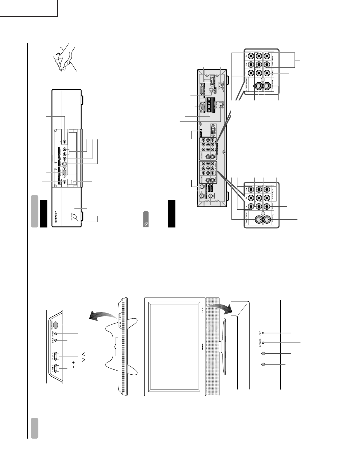
Part names
OPC indicator*
POWER indicator
MAIN POWER
button
OPC sensor
Display
POWER button
INPUT
button
VOLUME buttons
(VOL
/
)
CHANNEL buttons
(CH
/
)
Remote control sensor
*OPC: Optical Picture Con trol
Front view
CLEAR*
MAIN POWER button
INPUT 4 terminal (S-VI DE O)
INPUT 4 terminal (VIDE O)
PC INPUT terminal (AUDIO)
INPUT 4 terminals (AUD IO L/R )
PC INPUT terminal (ANALOG RGB)
AVC System
Rear view
INPUT 1 COMPONENT
video terminals (Y, P
B
, P
R
)
INPUT 3 COMPONENT
video terminals (Y, P
B
, P
R
)
MONITOR OUTPUT termin al
(S-VIDEO)
DISPLAY OUTPUT 1 terminal
DISPLAY
OUTPUT 2
terminal
AC I
NPUT
terminal
RS
-232C
terminal
MONITOR OUTPUT terminals (AUDIO L/R)
Antenna (A)
input terminal
Antenna (B)
input terminal
Antenna (A) output
terminal
DVI-HDTV
INPUT
terminal
INPUT 3 terminal (S-VI DE O)
INPUT 3 terminal (VIDE O)
INPUT 3 terminals (AUD IO L/R )
INPUT 1 terminal (S-VI DE O)
INPUT 1 terminal
(VIDEO)
INPUT 1 terminals
(AUDIO L/R)
INPUT 2 terminal (S-VI DE O)
INPUT 2 terminal (VIDE O)
INPUT 2 terminals
(AUDIO L/R)
How to open the door.
STANDBY/ON indicator
* If the AVC System is switched on but it does not appear to be operating correctly, it may need resetting. In this
case, press CLEAR, shown in the diagram, lightly with the end of a ballpoint pen or other pointed object.
This will reset the System as shown below.
• AV MO DE reset s to USE R
• TV channel returns to initial channel setting (Air:2ch, Cable:1 or 2ch)
• Twin pi ct ure resets to no rmal
• Audio setting initializes
• Dolby virtual resets to Off
• Image position initializes
NOTE
• Pressing CLEAR will not work if the System is in standby mode (indicator lights red).
• Pressing CLEAR will not delete channel preset or secret number. See page 61 for clearing the secret number when you
know it.
See page
for initializing to the factory preset values when you forget your secret number.
Headphone
(When connecting headphones, the sound from the
speakers is muted.)
DC OUTPUT terminal
(Terminal for expanded functionality in
the near future.)
MONITOR OUTPUT
terminal (VIDEO)
DISPLAY OUTPUT 3 terminal
EXTERN
AL SPEAKER terminals
OPERATION MANUAL
6
Page 7
LC-37HV6U
Part names
Remote control unit
NOTE
• When using the remote control unit, po in t it at th e Li qu id
Crystal Television.
• See pages for operating buttons not listed on this page.
TV
ANT-A/B
INPUT
Virtual
TWIN
MODE
AV
POWER
MTS CC
PICTURE
SELECT
SUB TWIN CH
+
—
FREEZE
MODE
VOL CH
MUTE
MENU TV/SAT/DVD
FAVORITE CH
RECEIVER
DTV/DVD TOP
SOURCE DTV/SAT
DTV/SAT
VCR REC
ABCD
RETURN
MENU
POWER
SET/
ENTER
MENU
GUIDE
INPUT VOL— VOL+
INFO
VIEW
SLEEP
LEARN
EDIT/
ENT
FLASHBACK
DISPLAY
INPUT
TV VCRCBL
/SAT
/DTV
DVD
/LD
123
456
789
100
0
POWER
16
17
18
19
20
21
22
24 25
23
3
2
1
4
5
6
7
8
9
10
11
12 13
14
15
1TVPOWER: Switch the Liquid Crystal Television power
on or off.
2
Virtual*: Select the Dolby virtual settings.
3 AV MODE: Select an audio or video setting.(AV mode:
DYNAMIC (Fixed), DYNAMIC,STANDARD, MOVIE,
GAME, USER. PC mode: STANDARD, USER.)
4 VIEW MODE: Select the screen si ze.
5DISPLAY: Display the channel information.
6SLEEP: Set the sleep timer.
7 FLASHBACK: Re tur n to th e prev ious chan ne l or inpu t
external mode.
8 VOL
+
/
–
: Set the volume.
9 MENU: Display the menu screen.
10 MENU RETURN: Return to the previous menu screen.
11
/
/
/
: Select a desired item on the screen.
12 ANT-A/B: Select between ANT-A and B to watch
broadcasts via the two tuners.
13 INPUT: Select a Liquid Crystal Television input source.
(TV, INPUT 1, INPUT 2, INPUT 3, INPUT 4, PC)
14
: When pressed all buttons on the remote contr ol unit
will light. The li ghting will tu rn off if no op erations are
performed within about 5 seconds. This button is used
for performing operations in dark places.
15 MTS: Sel ec t th e MT S/ SA P.
16 CC: Display captions during closed-caption source.
17 TWIN CH buttons
TWIN PICTURE: Set the twin picture mode.
Press again to return to no r ma l sc reen .
FREEZE: Set th
e still image. Press agai n to return to
normal screen.
SELECT: Select the active screen.
SUB INPU
T:
Select
an input source of sub screen.
TWIN CH
/
: Sel
ect the channel of sub screen.
18
0
– 9: Se
t the channel.
19 100 ENT: Select the three digit mode. Execute a
command of the channel.
20 CH
/
: Select the channel.
21 MUTE: Mute the sound.
22 SET/ENTER:
Execute a c
ommand.
23 FAVORITE CH
A, B, C, D: Select four preset favo ri te ch anne ls in fo ur
different categories.
When view
ing via ANT-A: up to 16 channe ls can be
assigned in A, B, C and D.
When viewing via ANT-B: up to 16 channels can be
assigned i
n A, B, C and D.
With AN
T-A and B combined, you ca n preset up to 32
favorite channels in advance.
While watching, you ca n to ggle the se le ct ed ch anne ls
by press
ing A, B, C and D.
24 LED for transmission confirmation
25 Mode switch
* VIRTUAL DOLBY SURROUND
Manufactured under license from Dolby
Laboratories."Dolby","Pro Logic" and the double-
D symbol are trademarks of Dolby Laboratories.
Preparation
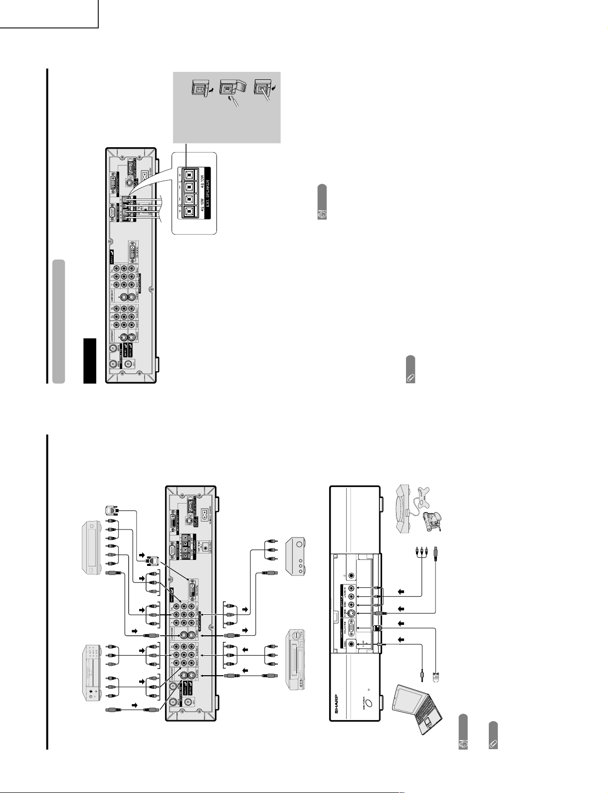
Removing the stand and speaker
This unit has detachable type speaker.
You can detach the system speaker when using external amplifier/speaker.
Before detaching (or attaching) speaker, unplug the AC cord from the AC outlet and the system cable from the
Display.
CAUTION
• When using the TV with the supplied stand attached, do not remove the speaker. Doing so may disturb
the balance leading to product damage or personal injury.
Before attaching/detaching speaker
• Before performing work make sure to turn off the System.
• Before performing work spread cushioning over the base area to lay the Display on. This will prevent it from
being damaged.
CAUTION
• The speaker terminals on the Display are only for the attached speaker. Do not connect any third party plug or speaker
to the terminal.
• Insert the speaker plug completely into the terminal.
NOTE
• To attach the spe ak er, perform the ab ov e st ep s in rever se order.
2
34
Unfasten the screws used to secure the speaker in
place.
Take hold of the speaker and slowly slide it
sideways.
(The speaker plugs are still inser ted, so make
sure not to pull the speaker too far.)
Remove the speaker plugs from the terminal on the
Display.
(Do not remove the plugs by pulling the cord.)
Now the speaker can be detached from the Display .
Speaker plug
1
Unfasten the screws used to sec ure the sta nd
in place, and then detach the stand from the
Display.
(Hold the stand so it will not drop the stand from
the edge of the base area.)
7
Page 8
LC-37HV6U
Setting the System in place
Handling the Display
CAUTION
• The Display is very heavy. Move it with two or more people.
• Do not remove the stand from the Display unless using an
optional bracket to mount it.
• Keep enough space above and behind the Display.
Handling the AVC System
CAUTION
• Do not put a VCR or other device on the AVC System.
• Keep enough space above and on the sides of the AVC System.
• Do not block the ventilation openings on the top and left side,
and the exhaust fan on the right side.
• Do not spr
ead a thick cloth beneath the AVC System, or cover it
with one, as this can cause overheating and result in
malfunction.
Where to place the System
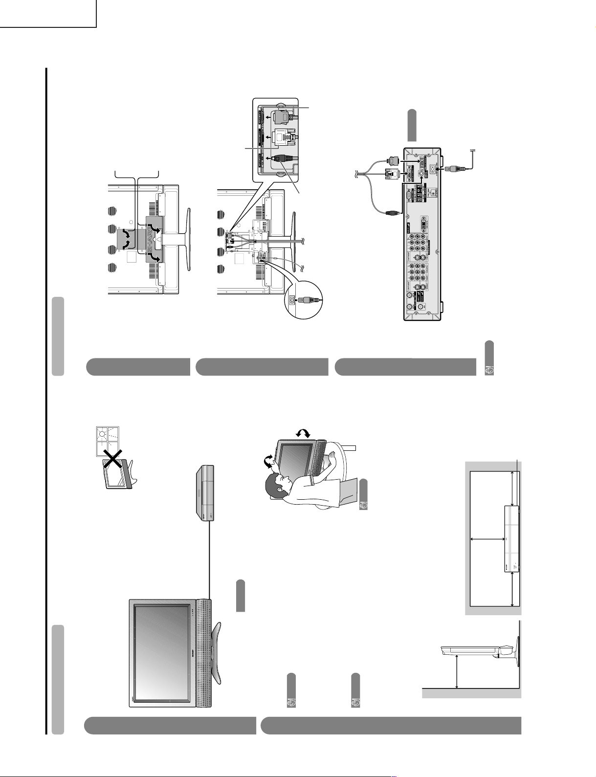
"System" means the Display and AVC System. First select the location where to place the System.
Selecting the location of the System
• Select a place with no direct sunlight and good ventilation.
• The Display and the AVC System are connected by the system cable.
Keep enough space
System cable
AVC System
Display
There is an
exhaust fan on
the right side.
1
2
4 inches
(10 cm)
or more
2 inches
(5 cm) or more
2 inches
(5 cm) or
more
Preparation
If you want to keep a longer distance between the Display and A
VC
System, please pur
chase the optional system cable AN-07SC1
(about 23 feet/7 meters).
IMPORTANT
• You cannot use external speakers when you are using the optional system
cable (AN-07SC1).
2 inches
(5 cm) or
more
CAUTION
Adjust the scre en wi th both
hands. Put one ha nd on the
Display and tilt th e screen
while steadying th e stan d
with your other hand .
You can adjust the sc reen
vertically up to 4 de grees
forward or 6 degree s back-
ward, or rotate 10 de grees
horizontally.
System cable
AVC System (rear view)
AC cord
Display (rear view)
Setting the System
After putting the Display and the AVC System in place, connect the system cables and AC cords. Use the
cable clamps for bundling the cables.
Connecting the system cable and the AC cord to the Display
1
2
3
Removing the terminal cover
Connecting the system cable and the AC cord to the AVC System
CAUTION
• TO PREVENT RISK OF ELECTR IC SHOC K, DO NOT TOUCH UN-INSULATED PARTS OF ANY CABLES WITH THE
AC CORD CONNECTED.
Press down the two
upper hooks to remove
the cover toward you.
Press the two hooks
toward the center of the
Display and remove the
cover toward you.
AC cord
(GLAY)
Connect the plug firmly until the
hooks on both sides clic k.
(WHITE)
Connect the plug into th e te rminal
and secure it by tightening the
thumb screws.
(BLACK)
(BLACK) (WHITE) (GLAY)
You cannot use external
speakers when you are using
the optional system cable
(AN-07SC1).
IMPORTANT
System cable
8
Page 9
LC-37HV6U
Preparation
4
5
Attaching the clamps and bundling the cables with the clamp
Closing the terminal cover
Cable clamp (Large)
Insert the cable
clamp in the hole
on the Display leg
as shown.
Cable clamp (Small)
Peel off the seal
on the back and
attach as shown.
Display (rear view)
Cables come
out from the
small opening.
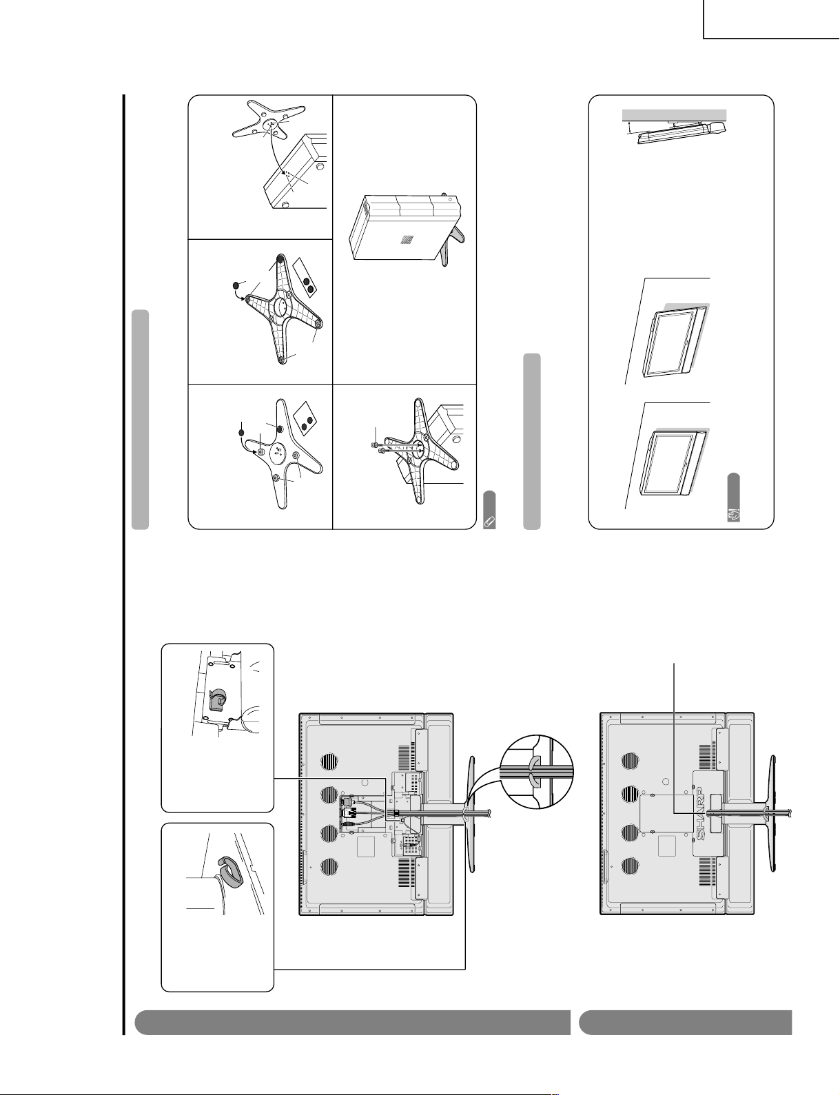
Setting the Display on the wall
CAUTION
• Installing the Liqu id Crystal T elevisio n requires spec ial skill that should only be performed by qualifie d service personnel.
Customers should no t attemp t to do th e work th emse lves. SH ARP be ars no respons ibil ity for im proper mo unti ng or
mounting that results in acc id en t or inj ury.
Using an optional brac
ket to mount the Display
• You can ask a qualified service personnel about using an optional AN-37AG1 bracket to mount the Display
to the wall.
• Carefully read the instructions that come with the bracket before beginning work.
Vertical mounting Angular mounting
Hanging on the wall
AN-37AG1 wall mount bracket. (See the bracket instructions for details.)
Setting the AVC System with the stand
1
How to install the A
VC System vertically using the stand unit.
• Use the supplied stand unit for installing the AVC System vertically in an upright position.
Stick each spacer to the
stand as shown.
Peel each spacer
away from the
paper and attach
to the four bulging
areas on the stand.
2
Attach each cushion to
the stand as shown.
3
Fit the stand to the AVC
System.
Peel each cushion
away from the
paper and attach
to the four areas at
the bottom.
Insert the stand in to the AVC
System, making sure that the
thick and thin bulge s of the
stand align with the big and
small holes on the AVC
System.
Stand
spacer
Bulge
Stand cushion
Thin bulge
Thick
bulge
Big hole
Small
hole
4
Attach the stand using the
stand screws as shown.
Stand screw
The AVC System installed
vertically with the stand.
NOTE
• When mounting the AVC System vertically, always use th e supp lied stan d. Be ca reful no t to bl ock vent ho les wh en
st
anding up directly on the floor or a flat surface as this can result in equipment failure.
Attaching point
Attaching point
Bulge
5°
About setting the Disp lay ang le
• You can set the Display on the
wa
ll up to 5 degrees forward
when the speaker is attached and
up to 20 degrees forward when
the speaker is not attached. Do
not set the angle outs id e th os e
ranges.
9
Page 10
LC-37HV6U
Using external equipment
Digital TV tuner
AVC System
(rear view)
AVC System
(front view)
AV Receiver
(Built-in Tuner Amp)VCR
DVD player
Game console/
Camcorder
PC
You can connect many types of external equipment to your System, like a DVD player, VCR, Digital TV tuner, PC,
game console and camcorder. To view external source images , select the input source from INPUT on the
remote control unit or on the Display.
CAUTION
• To protect all equipment, always turn off the AVC System before connecting to a DVD player, VCR, Digital TV tuner,
PC, game console, camc orde r or oth er ext ernal equipment.
NOTE
• Please refer to the relevant operation manual (DVD player, PC, etc.) carefully before making connections.
S-VIDEO
S-VIDEO
S-VIDEO
AV
S-VIDEO
AV
AV
AV
Y/P
B
/P
R
Y/P
B
/P
R
PC-AUDIO
ANALOG RGB
AV
S-VIDEO
DVI
Rear view
Useful adjustment settings
Connecting external speakers
When using external speakers
• Change the speaker setting to exter nal speakers.
Make sure to connect the speaker terminal and
cable polarity (
+
, –) properly
•
The speaker terminals have plus (
+
) and minus (
–
)
polarity.
• Plus is red and minus is black.
• The cables are also divided into plus and mi nu s.
• When connecting the left/right speakers, be sure to
connect the plus/minus terminals with the correct cables.
NOT
E
• Unplug the AC cord from the AC outlet be fore instal ling
the speakers.
CAUTION
• Make sure external speakers have 4 ohm and 10 watt
specifications.
• Connect the plus/minus terminals with the correct cables.
Incorrect connection ma y ca us e a sh ort.
How to connect the
speaker cable
Push down
the tab.
Insert the
end of the
cable.
1
2
3
Lift the tab
back up.
10
Page 11
Basic adjustment settings
AV input mode menu items
List of AV menu items to help you with
operations
OPC
Backlight
Contrast
Black Level
Color
Tint
Sharpness
Advanced
C.M.S.
Color Temp
Black
3D-Y/C
Monochrome
Film Mode
I/P Setting
Picture
No Signal Off
No Operation Off
EZ Setup
CH Set
up
Speaker
Input Signal
Parental CTRL
Position
Picture Flip
Language
Treble
Bass
Balance
Dolby Virtual
Audio Only
Input Select
DNR
Audio Out
Quick Shoot
Audio
Power control
Setup
Option
PC input mode menu items
List of PC menu items to help you with
operations
OPC
Backlight
Contrast
Black Level
Red
Green
Blue
C.M.S.
Picture
Power Management
Input Signal
Speaker
Auto Sync.
Fine Sync.
Picture Flip
Language
Audio
Power control
Setup
Treble
Bass
Balance
Dolby Virtual
Option
Audio Only
Audio Out
Quick Shoot
Appendix
PC compatibility chart
Apple and Macintosh are registered tradem arks
of Apple Computer, Inc.
DDC is a registered trademark of V ideo Electronics
Standards Association.
Power Management is a registered trademark of
Sun Microsystems, Inc.
VGA and XGA are registered trademarks of
International Business Mac hin es Co. , Inc.
PC/MAC Resolution
Horizontal Frequency
Vertical Frequency
VESA Standard
PC
31.5 kHz
37.9 kHz
31.5 kHz
37.9 kHz
31.5 kHz
37.9 kHz
37.5 kHz
43.3 kHz
31.5 kHz
35.1 kHz
37.9 kHz
48.1 kHz
46.9 kHz
53.7 kHz
48.4 kHz
56.5 kHz
60.0 kHz
68.7 kHz
45.0 kHz
48.1 kHz
64.0 kHz
34.9 kHz
49.7 kHz
60.2 kHz
640 x 400
720 x 400
VGA
640 x 480
WVGA 848 x 480
SVGA
800 x 600
1024 x 768XGA
1280 x 720
WXGA
1280 x 768
SXGA
1280 x 1024
VGA
640 x 480
MAC13"
XGA
1024 x 768
MAC19"
SVGA
832 x 624
MAC16"
60 Hz
85 Hz
60 Hz
85 Hz
60 Hz
72 Hz
75 Hz
85 Hz
60 Hz
56 Hz
60 Hz
72 Hz
75 Hz
85 Hz
60 Hz
70 Hz
75 Hz
85 Hz
60 Hz
60 Hz
60 Hz
67 Hz
75 Hz
75 Hz
O
O
O
O
O
O
O
O
O
O
O
O
O
O
O
O
LC-37HV6U
11
Page 12
LC-37HV6U
Command table
• About the command except being indicated here, it is outside the guarantee range of operation.
CONTROL ITEM COMMAND
PARAMETER
CONTROL CONTENTS
POWER SETTING It shifts to standby.
It input-switches by the toggle. (It is the same as an input change key)
It input-switches to TV. (A channel remains as it is. (Last memory))
It input-switches to INPUT1~INPUT4.
It input-switches to PC.
An input change is also included.
Although it can choose now, it is toggle operation in inside.
Although it can choose now, it is toggle operation in inside.
(Toggle)
Input terminal number (1–4)
AUTO
AV-Y/C
COMPONENT
AUTO
AV-Y/C
COMPONENT
DVI
(Toggle)
STANDARD
DYNAMIC
MOVIE
DYNAMIC (Fixed)
GAME
USER
Volume (0–60)
AV mode. ( ± 10)
PC mode. (± 90)
AV mode. (± 30)
PC mode. (± 60)
Only PC mode. (± 90)
Only PC mode. (± 20)
(Toggle) [AV]
Toggle operation.
An input change is included if it is not TV display.
In Air, 2–69ch is effective.
In Cable, 1–125ch is effective.
If it is not TV display, it will input-switch to TV.
If it is not TV display, it will input-switch to TV.
Change toggle operation of tuner A/B.
Toggle operation of a closed caption.
(Toggle)
Side Bar [AV]
S.Stretch [AV]
Zoom [AV]
Stretch [AV]
Normal [PC]
Stretch [PC]
Dot by Dot [PC]
Zoom [PC]
(Toggle)
Off
SRS
FOCUS
FOCUS
+
SRS
One screen
Twin screens
The channel number of TV
The channel number of TV + 1
The channel number of TV —1
(Toggle)
(Toggle)
OFF
CC1
CC2
T1
T2
(1~125)
AUTO
POWR
ITGD
ITVD
IAVD
IPCD
INP1
INP3
INPUT SELECTION A TOGGLE
INPUT SELECTION B
AV MODE SELECTION
VOLUME
POSITION
VIEWMODE
SRS
TWIN PICTURE
CHANNEL
ANT-A/B
CC
DIRECT
CH UP
CH DOWN
CHANNEL
H-POSITIONH-POSITION
V-POSITION
CLOCK
PHASE
INPUT 1
INPUT 3
AVMD
VOLM
HPOS
VPO
S
CLCK
PHSE
SRSS
TWI
N
DCCH
CHUP
CHDW
ANTS
CLCP
WI
DE
0
x
0
*
x
0
0
1
2
3
1
2
0
*
*
*
*
*
0
0
*
x
x
x
0
1
2
3
4
5
1
1
2
3
4
0
1
2
3
4
5
6
7
8
*
*
1
2
3
4
5
6
*
_
_
_
_
_
_
_
_
_
_
_
_
_
_
_
_
_
_
_
_
_
_
_
_
_
*
*
*
*
*
*
*
_
_
_
_
_
_
_
_
_
_
_
_
_
_
_
_
_
_
_
*
_
_
_
_
_
_
_
_
_
_
_
_
_
_
_
_
_
_
_
_
_
_
_
_
_
*
*
*
*
*
*
_
_
_
_
_
_
_
_
_
_
_
_
_
_
_
_
_
_
_
_
_
_
_
_
_
_
_
_
_
_
_
_
_
_
_
_
_
_
_
_
_
_
_
_
_
_
_
_
_
_
_
_
_
_
_
_
_
_
_
_
_
_
_
_
_
_
_
_
_
_
_
_
TV
INPUT1-4
PC
NOTE
• If an underbar (_) appears in the parame te r co lu mn , en te r a sp ac e.
• If an asterisk (*) appears, enter a value in the range indicated in brackets under CONTROL CONTENTS.
• As long as that from which the parameter ( × ) in the table is a numerical value, it may write anything.
Return code (0DH)
Response code format
Normal response
Problem response (communication error or incorrect command)
Return code (0DH)
OK
ERR
RS-232C port specifications
Return codeCommand 4-digits Parameter 4-
digits
PC Control of the System
• When a program is set, the Display can be controlled from the PC using the RS-232C terminal.
The input signal (PC/AV) can be selected, the volume can be adjusted and various other adjust ments and
settings can be made, enabling automatic programmed playing.
•
Attach an RS-232C cable cross- type (commercially available) to the supplied Din/D-Sub RS- 232C for the
connections.
NOTE
• This operation system should be used by a person who is accustomed to using computers.
Communication conditions
Set the RS-232C communications settings on the PC to match the display’s communications conditions.
The Display’s communications settings are as follows:
Baud rate:
Parity bit:
Data length:
Stop bit:
Flow control:
9,600 bps
8 bits
None
1 bit
None
Appendix
Comman
d format
Communication procedure
Send the control commands from the PC via the RS-232C connector.
The display operates according to the received command and sends a response message to the PC.
Do not send multiple commands at the same time. Wait until the PC receives the OK response before sending
the next command.
Eight ASCII codes + CR
Comm
and 4-digits:Comma nd. Th e text of four charac ters .
Parameter 4-digits :Par am eter 0 – 9, x, bl an k, ?
Parameter
Input the parameter va lu es , al ig ni ng lef t, and fil l wi th bla nk (s ) fo r th e remai nd er. (Be sure that 4 values are in pu t for the
parame
ter.)
When the i
nput parameter is not within an adjustable range, "ERR" returns. (Refer to "Response code format".)
No problem to input any numerical value for "x" on the table.
When "?" is input for some commands, the present setting value responds.
C1 C2 C3 C4 P1 P2 P3 P4
0055
100
–
30
0009
0
????
?
12
Page 13
DIMENSIONS
LC-37HV6U
AVC System
1423/64(365)
59
/64(430)
16
(95)
64
/
47
3
927/32(250)713/64(183)
75/64(180)
Unit: inch/(mm)
(5)
16
/
3
13
Page 14
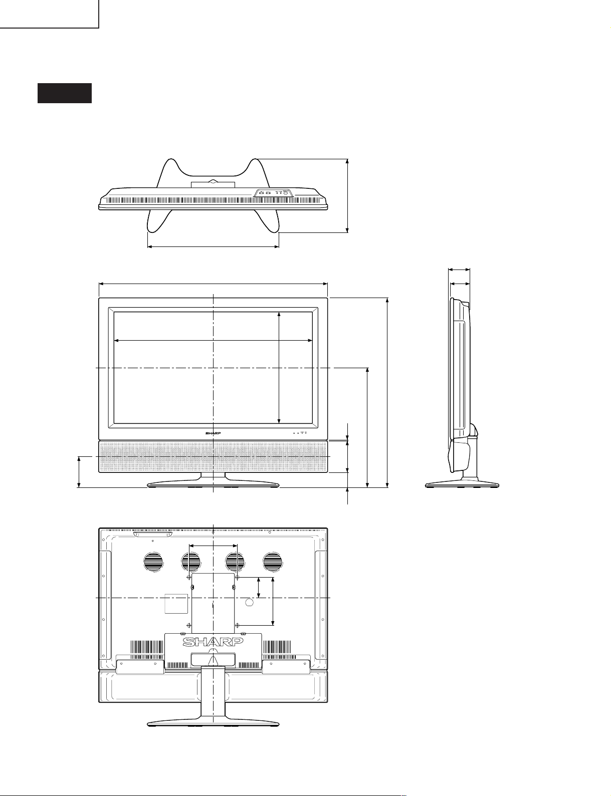
LC-37HV6U
Display
Unit: inch/(mm)
12 (305)
29
21
/
64
(545)
35
3
/
64
(90)
7
3
/
21
37
/
64
(948)
11
32
/
32
(821.6)
(82)
32
5(127)
(495.5)
2
/
1
19
(784)
64
/
55
30
(462.8)
32
/
7
18
(5)
16
/
3
(130)
64
/
7
16
/
7
(62) 5
2
7
7
/
8
(200)
32
/
11
(85)
3
(200)
8
/
7
7
14
Page 15
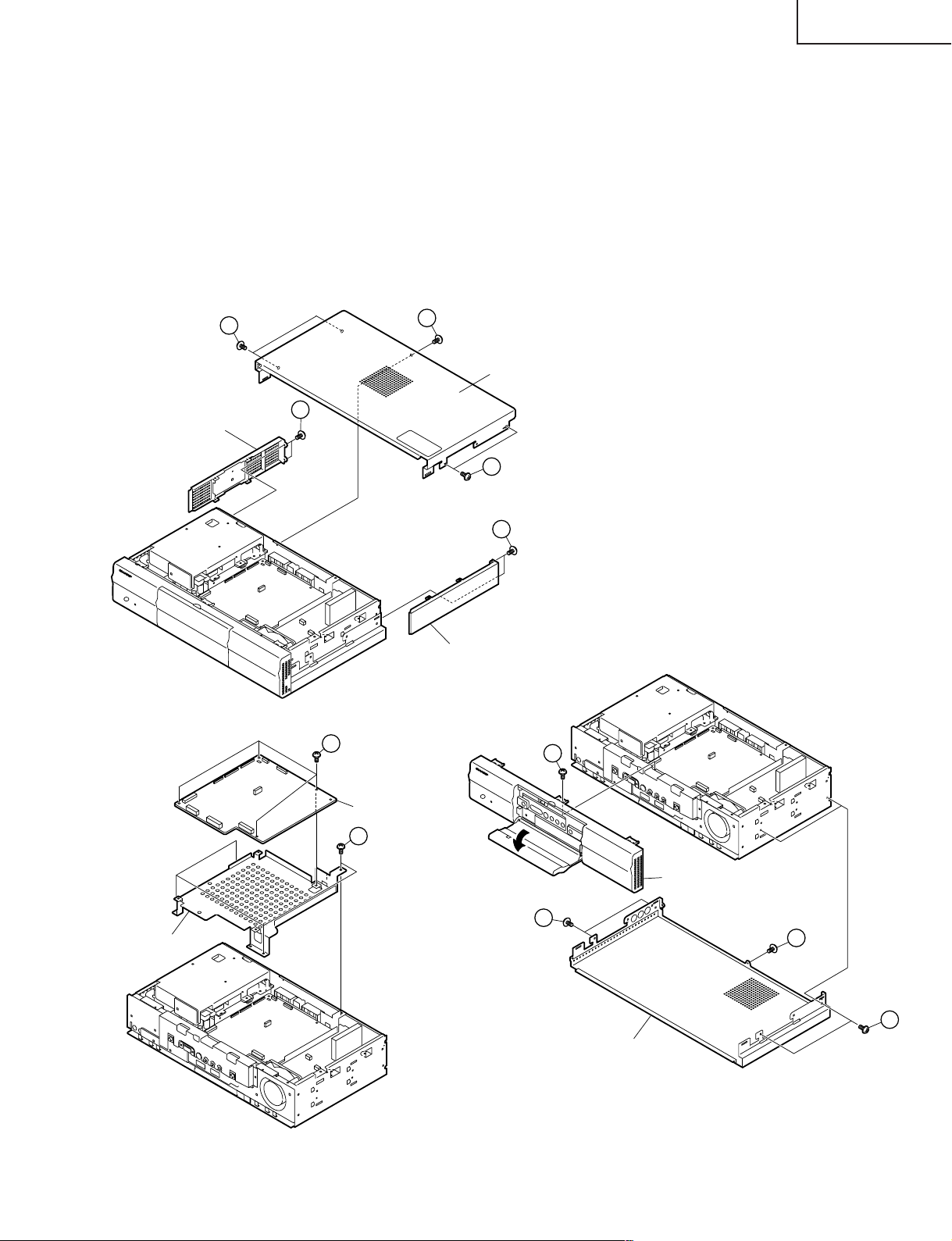
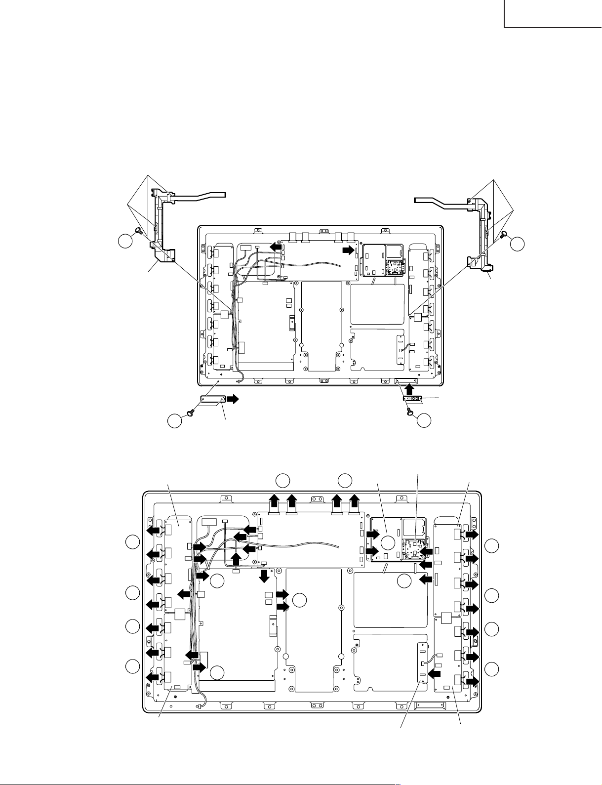
REMOVING OF MAJOR PARTS
Ë Ë
Ë AVC System
Ë Ë
1. Remove the five top cabinet retaining screws and slide the top cabinet backward to remove it.
2. Remove the four side cover retaining screws on both the right and left sides and slide the side covers
backward to remove them.
3. Remove the one front panel retaining screws and remove the front panel.
4. Remove the five bottom cabinet retaining screws and slide the bottom panel backward to remove it.
5. Remove the four screws securing the main PWB angle and remove the angle upward.
6. Remove the four screws securing the main PWB to the angle and remove the main PWB.
LC-37HV6U
1
Side Cover (L)
1
Top Cabinet
2
1
2
Side Cover (R)
6
3
Main PWB Angle
Main PWB
5
Front Panel
4
4
4
Bottom Panel
15
Page 16

LC-37HV6U
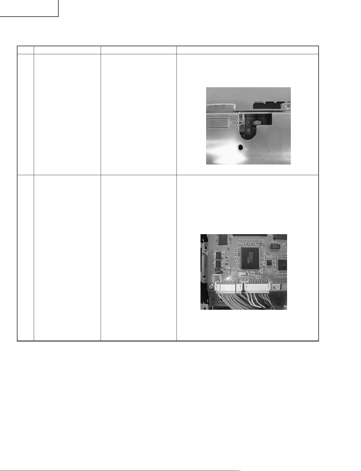
7. Remove the system/control terminal retaining:
7-1. Remove the four hex head screws securing the terminals of the system and control cables (white).
7-2. Remove the four screws securing the terminal of the system cable (gray).
7-3. Remove the four rear chassis retaining screws.
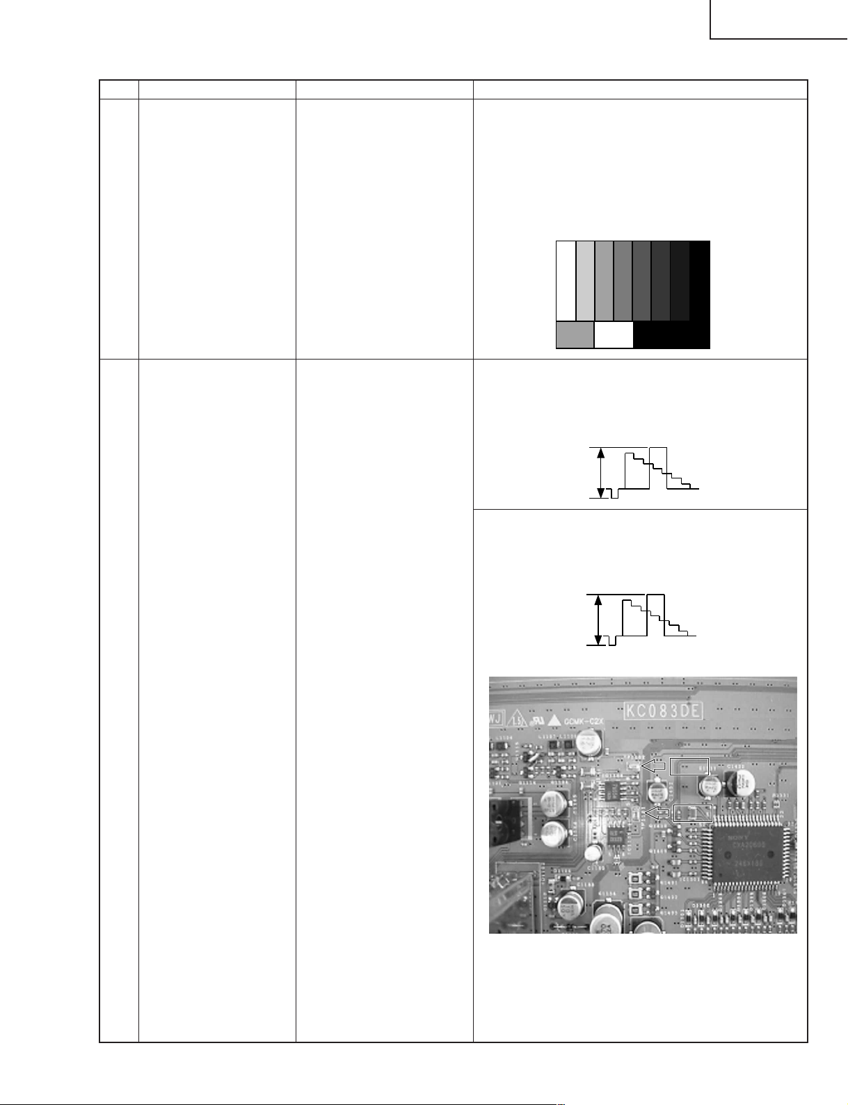
8. Remove the PC I/F and Audio I/F units:
8-1. Remove the five PC I/F top shield retaining screws and remove the shield.
8-2. Remove the six PC I/F unit retaining screws and remove the unit.
8-3. Remove the two PC I/F bottom angle retaining screws and remove the angle.
8-4. Remove the two Audio I/F unit retaining screws and remove the Audio I/F unit.
9. Remove the rear chassis.
9-1. Remove the three tuner nuts.
9-2. Remove the 13 rear cabinet retaining screws and remove the rear cabinet.
10. Remove the three power unit retaining screws and remove the power unit.
8-1
8-2
PC I/F Top Shield
PC I/F unit
Audio I/F unit
8-4
8-3
PC I/F Bottom Angle
7-1
7-3
7-2
Rear Cabinet
10
9-2
9-2
9-2
Power Unit
9-2
9-1
9-2
16
Page 17
11. Remove the AV unit:
Cooling Fan
12-1
11-1. Remove the five AV unit retaining screws and remove the AV unit.
11-2. Remove the three AV unit angle retaining screws and remove the angle.
12. Remove the fan:
12-1. Remove the two cooling fan retaining screws and remove the cooling fan.
13. Remove unit from the front chassis:
13-1. Remove the two hex head screws and four screws securing the front shield to the front chassis and
remove the front shield.
13-2. Remove the four screws securing the front unit and remove the unit.
11-1
AV Unit
AV Unit Angle
11-2
LC-37HV6U
13-1
13-1
Front Shield
13-2
Front Unit
17
Page 18
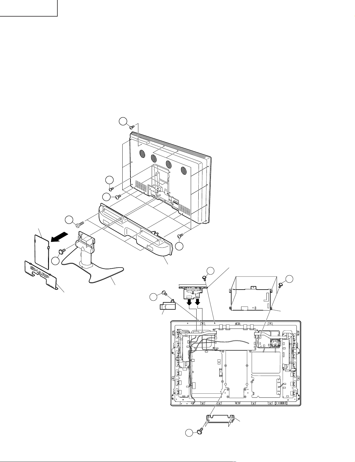
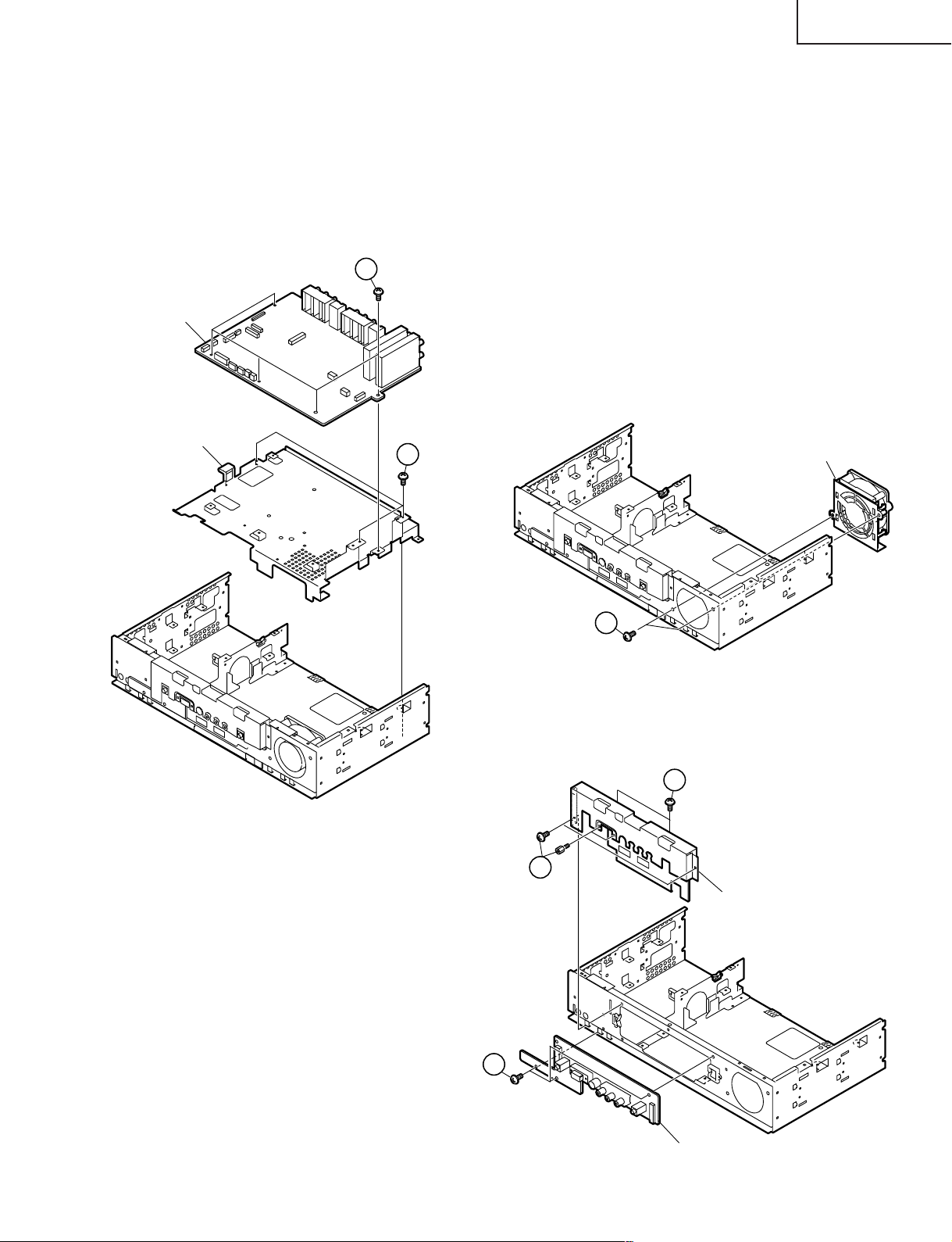
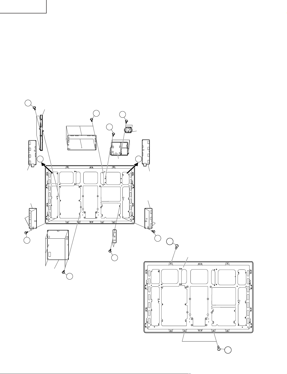
LC-37HV6U
Ë Ë
Ë Display
Ë Ë
1. Remove the top and bottom terminal covers.
2. Remove the four lock screws from the speaker. Disconnect the speaker terminals and detach the speaker.
3. Remove the four lock screws from the stand, and detach the stand.
4. Remove the 18 lock screws from the cabinets A and B, and remove the cabinet B.
5. Remove the two lock screws from the operation PWB assembly, and detach the operation PWB assembly.
6. Remo v e the lock screw from the operation PWB insulating sheet, and detach the operation PWB insulating sheet.
7. Remove the seven lock screws from the main PWB shield, and detach the main PWB shield.
8. Remove the four lock screws from the stand fixture, and detach the stand fixture.
4
Terminal Cover (Top)
3
Terminal Cover (Bottom)
4
4
2
1
4
Speaker
Stand
6
Operation PWB Insulating Sheet
P152
5
P151
Operation PWB Assembly
7
Main PWB Shield
18
Stand Fixture
8
Page 19
LC-37HV6U
FFC Holder (Left)
FFC Holder (Right)
Cable Holder
Cable Holder
Speaker Jack PWB
R/C, LED PWB
P101
CN4101
CN4102
9
11
10
9
9. Open the six FFC holders. Remo ve the three lock screws from each of the right and left FFC holders. Disconnect
all the FFC connectors and detach the right and left FFC holders.
10.Remove the two lock screws from the speaker jack PWB, disconnect the connector, and detach the speaker jack
PWB.
11.Remove the two lock screws from the R/C, LED PWB, and detach the R/C, LED PWB.
12.Disconnect the connectors from each PWB. (13 from the monitor PWB, 5 from the power PWB, 6 from the audio
PWB, 7 from the inv erter-1 PWB, 5 from the inverter-2 PWB, 7 from the inv erter-3 PWB, 6 from the inv erter-4 PWB,
2 from the 1-Bit amplifier unit, and 1 from the thermistor PWB)
1-Bit Amplifier Unit
Inverter-1 PWB
12
P7505
P7506
P7507
12
12
CN3701
12
CN3782
CN3702
Power PWB
CN4701
CN4702
12 12
SC4601 SC4604
SC4603
CN4101
CN7004
CN2004
CN2002
Monitor PWB
12
Audio PWB
SC4602
CN7705
CN2003
12
12
12
P7554
CN2702
12
Inverter-2 PWB
Thermistor PWB
19
Inverter-3 PWB
P7616
P7619
P7618
P7647
P7644
Inverter-4 PWB
12
12
12
12
Page 20
LC-37HV6U
13. Remove the eight lock screws from the Monitor PWB, and detach the main PWB.
14. Remove the six lock screws from the power PWB, and detach the power PWB.
15. Remove the four lock screws from the audio PWB, and detach the audio PWB.
16. Remove the three lock screws from the holder, and detach the holder.
17. Detach the inverter-1 PWB.
18. Remove the three lock screws from the inverter-2 PWB, and detach the inverter-2 PWB.
19. Detach the inverter-3 PWB.
20. Remove the three lock screws from the inverter-4 PWB, and detach the inverter-4 PWB.
21. Remove the two lock screws from the thermistor PWB, and detach the thermistor PWB.
22. Remove the two lock screws from the 1-Bit amplifier unit, and detach the 1-Bit amplifier unit.
23. Remove the three lock screws from the chassis, and detach the chassis.
16
Inverter-1 PWB
Inverter-2 PWB
18
Holder
13
17 19
Monitor PWB
22
15
Audio PWB
Thermistor PWB
1-Bit Amplifier Unit
Inverter-3 PWB
Inverter-4 PWB
20
23
Power PWB
21
Chassis
14
23
20
Page 21
LC-37HV6U
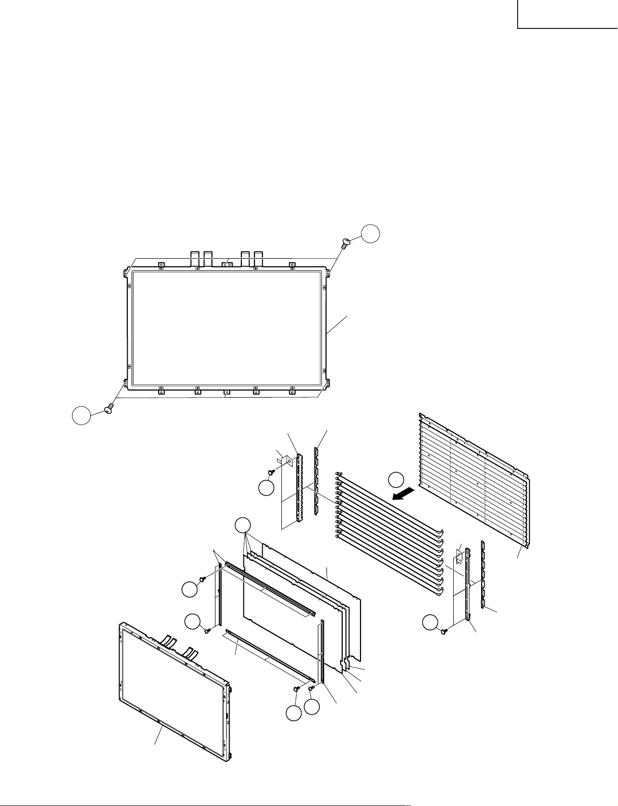
• Precautions in handling the liquid crystal panel
1. Handle the liquid crystal panel in a clean room (Humidity: 50% or more).
2. Be sure to wear an earth wristband.
3. Be careful not to drop and shock the liquid crystal panel.
4. Use an ionizer (within 30 cm).
24.Remove the six lock screws from the LCD panel, and detach the LCD panel unit.
25.Remove the three lock screws from each of the sheet fixtures, and detach the sheet fixtures.
26.Detach the reflection/deflection sheet, prism sheet, diffusion sheet and diffusion panel.
27.Remove the three lock scre ws from each of the top and bottom lamp holders , and detach the top and bottom lamp
holders.
28.Detach the lamp assembly from the lamp clip.
23
23
Sheet fixture
24
Lamp Holder (Top)
Panel bracket
26
25
LCD Panel Unit (Front)
Lamp Holder (Bottom)
Lamp Unit
Diffusion Panel
27
Panel
bracket
Reflection Panel
LCD Panel Unit
24
Sheet fixture
24
24
Sheet fixture
21
26
Lamp Holder (Bottom)
Lamp Holder (Top)
Diffusion Sheet
Prism Sheet
Reflection/Deflection Sheet
Page 22

LC-37HV6U
ADJUSTMENT PROCEDURES (AVC SYSTEM)
Preparation for adjustment
1. The product has been adjusted and optimized in the factory. If the product needs to be readjusted for some
reason, e.g., after parts replacement, follow the instructions shown below.
2. Control parameter values set in the in-process adjustment mode has been stored in the corresponding registers.
When the product is readjusted, the contents of the registers are changed. Bef ore readjustment, f actory settings
should be noted in case the contents of registers require to be restored.
3. Use a stabilized AC power supply.
4. To rewrite a program, you should note the items ("OSD MENU" and "Adjustment Values") you want to change
and initialize EEPROM, and then rewrite the changes into EEPROM.
How to enter the in-process adjustment mode
CAUTION: Exercise great care to hide the procedure in entering the in-process adjustment mode from the
customer. Inadvertent setting changes in this mode may cause a fatal error resulting in a program being
unrecoverable.
1. Entering the in-process adjustment mode:
Connect the system cable between the display and AVC system.
Turn off the "MAIN POWER" button of the display once.
Turn on the main power while holding down the "INPUT" button and the "VOL (-)" button of the Display
simultaneously.
The system will be activated.
~If you see multiple lines of blue characters on the display, you are in the in-process adjustment mode. If not
(the normal activation screen opens), retry.
2. Accessing the inspection process mode:
After activation of the system, make adjustments according to the instructions indicated on the process
adjustment OSD menu screen.
Move to the General Process Adjustment (AVC System Section Process).
3. Restoring factory settings: (At the time of "INDUSTRY INIT" execution, please wait for about 30 seconds until
/// disappears.)
When the "INDUSTRY INIT" button is selected after activation of the system, factory channel setting remains
unchanged.
After the system exits from the in-process adjustment mode.
Changes made by the user will default to factory settings. Note that channel setting is also initialized.
4. Exiting from the in-process adjustment mode:
Unplug the power cable while the system is in the in-process adjustment mode to exit from the mode.
Take care not to press the "POWER" button on the remote controller or the AVC system after using factory
settings to run the system.
5. OSD menu screen and menu items during manual adjustment:
~The layout and men u items of the OSD menu screen ma y somewhat v ary depending on the program versions.
~Just rewriting a program does not cause settings to be "initial values". (Preparation for adjustment)
1. Button operation in the in-process adjustment mode
Cursor Up Move to the next page
Cursor Down Back to the previous page
Volume (+) Increase the setting by 1
Volume (-) Decrease the setting by 1
SET/ENTER Execute the function
Cursor Left Increase the setting by 10
Cursor Right Decrease the setting by 10
Channel (Up) Move the cursor up
Channel (Down) Move the cursor down
INPUT Change input (Tuner-A ->Tuner-B -> Input 1 -> Input 2 ->Input 3 -> Input 4 -> PC ->)
22
Page 23
2. In-process adjustment screen layout
Page Source of input Color system HDCP Model name
1/13 INPUT2 N358 HDCP: OFF MONITOR: LC-37HV6U
KEY WRITE ON
INDUSTRY INIT OFF
CENTER Version 1.01 (U 2003/09/12 A )
OSD Version 1.00 (J 2003/06/20 A )
CVIC Version W2002/11/27 11:33 X2002/11/27 13:53
V2002/04/19 11:26 S2002/11/27 13:49
MONITOR Version 7A.7A7A
ModelSelect MAIN 2
ModelSelect AV 4
LC-37HV6U
ModelSelect MONITOR xx
STANDBY TYPE 0
HOTEL MODE OFF
6. Loading the backup data and setting HDCP when the PC I/F unit is replaced
Nearly all data including factory settings, user settings, and channel setting is stored in the PC I/F unit.
The product comes with EEPROM (IC1506) on the Main Unit in case the PC I/F unit is replaced; original data
backed up on the EEPROM can be loaded to the new PC I/F unit.
∫ How to load the backup data
Select EEPROM RECOVER in the OSD menu (page 7) and turn the "Volume" key ON; then press "SET/
ENTER".
∫ How to set HDCP
After completion of adjustments, select KEY WRITE "ON" in the OSD menu (page 1/13) f or manual adjustment
and turn the "Volume" key ON; then press "SET/ENTER".
∫ How to read the factory settings (backup data)
Select EEPROM RECOVER (page 7), set it from "OFF" to "ON" with the "Volume" key, and then press the
"SET/ENTER" key.
∫ Adjustments required after reading the factory settings
1) Page 2
Ë +Badj3.3V Adjustment of reference voltage
Ë +Badj1.8V Adjustment of important component operating voltage (It is adjusted automatically by pressing
the "SET/ENTER" key after performing 3.3V adjustment.)
2) Page 8 to Page 10
Ë N358 WB adjustment White balance adjustment (TV, VCR, etc.)
Ë COMP 15K WB adjustment White balance adjustment (Component 480i)
Ë COMP HDTV WB adjustment White balance adjustment (Component 1080i)
23
Page 24
LC-37HV6U
1) Analog adjustment
(1) V oltage adjustment
Item Adjusting conditions/points Adjusting procedure
1 3.3 V Adjustment Page: 2 • Connect a DC voltmeter to TP4 on the PC I/F unit.
Location: TP4
Move the cursor to
and (–)
keys to adjust the voltage to 3.30 ± 0.01 V.
TP4TP4
"Ë
+Badj.3.3V" and use
"VOL" (
+)
2 1.8 V Adjustment Page: 2 • After adjustment to 3.3 V, move the cursor to the
Location: Pin (6) of CN9 "Ë+Ba dj.1.8V" l i ne and pre ss the "ENTER" key on
the remote controller. Adjustment will be made
automatically.
If "ERR" appears, adjust the voltage at pin (6) of
CN9 on the PC I/F unit to 1.90 ± 0.01 V.
11
CN9CN9
1313
24
Page 25
(2) Tuner adjustment
TP1102TP1102
TP1101
TP1101
Item Adjusting conditions/points Adjusting procedure
1 Signal setting Signal: • Use a signal generator to provide the tuner with a
NTSC RF Signal RF signal of 193.25 MHz on the split field color bar.
(Split field color bar)
Input terminals:
•
The color saturation of the color bar must be 75%.
A 100% white area must be included.
ANT-A, ANT-B • Make sure the 100% white area (synchronized)
US channel 10 received shows 2.00 Vp-p when the color bar opens in
video mode. If not, adjust the signal generator.
2 Tuner level Adjustment Page: 4 1.Provide the above RF signal to ANT-A and adjust
Locations: TP1101, TP1102
"TUNERA DAC ADJ" so that the tuner output is
1.0 ± 0.02 Vp-p at TP1101 when US channel 10 is
received.
LC-37HV6U
1.0Vp-p
2.Provide the above RF signal to ANT-B and adjust
"TUNER B DAC ADJ" so that the tuner output is
1.0 ± 0.02 Vp-p at TP1102 when US channel 10 is
received.
1.0Vp-p
25
Page 26
LC-37HV6U
0.7Vp-p
0.525Vp-p
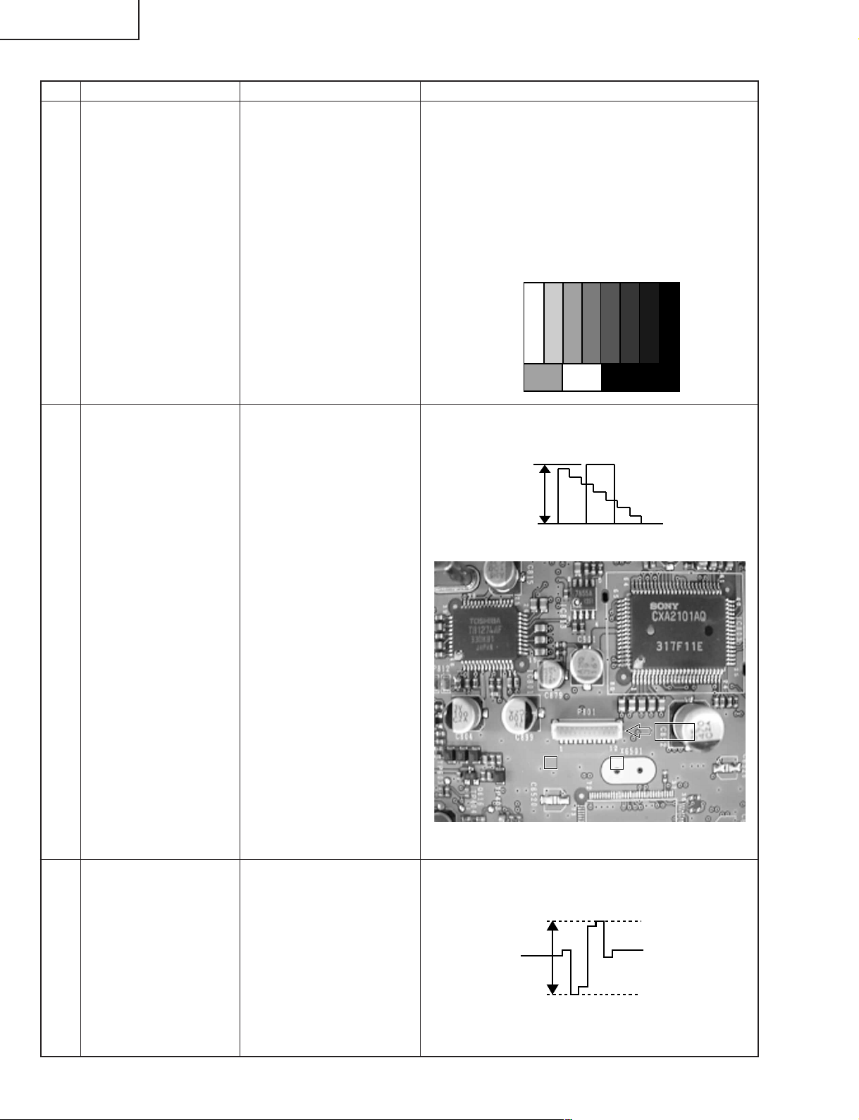
(3) NTSC signal adjustment
Item Adjusting conditions/points Adjusting procedure
1 Signal setting Signal: • Use a signal generator to provide the split field color
NTSC bar to the video image input pin of video input 1.
Split field color bar
•
The color saturation of the color bar must be 75%. A
100% white area must be included.
• Make sure the 100% white area (synchronized)
shows 2.00 Vp-p when the color bar opens in
video mode. If not, adjust the signal generator.
2 MAIN N358 Y Page: 3 Adjust "MAIN N358 Y GAIN" so that the 100%
GAIN Adjustment Signal pin: INPUT1, video white area shows 0.7 ± 0.01 Vp-p at pin (1) of P801.
Location: Pin (1) of P801
P801P801
11
1312
3 MAIN N358 CB Page: 3 Adjust "MAIN N358 CB GAIN" so that the width
GAIN Adjustment Location: Pin (3) of P801 shown below is 0.525 ± 0.01 Vp-p at pin (3) of P801.
26
Page 27
LC-37HV6U
Smoothed
1.0Vp-p
Smoothed
Item Adjusting conditions/points Adjusting procedure
4 MAIN N358 TINT Page: 3 Adjust "MAIN N358 TINT" so that the bottom edges
Adjustment Location: Pin (3) of P801 of the waveform at pin (3) of P801 are in line with
each other as shown below.
5 MAIN N358 CR GAIN Page: 3 Adjust "MAIN N358 CR GAIN" so that the width
Adjustment Location: Pin (5) of P801 shown below is 0.525 ± 0.01 Vp-p at pin (5) of P801.
0.525Vp-p
6 MAIN Page: 3 Adjust "MAIN CONTRAST 15K" so that the
CONTRAST 15K Location: Pin (7) of P801 difference between black and while peaks is
Adjustment 0.95 ± 0.02 V at pin (7) of P801.
7 Two-screen setting Press the TWIN PICT- Make the adjustment-purpose special two-screen
URE key. setting.
(The same images should appear on the main and
sub screens.)
8 SUB N358 Y Page: 4 Adjust "SUB N358 Y CONTRAST" so that the
CONTRAST Adjustment Location: Pin (9) of P801 difference between the black and white peaks is
1.0 ± 0.02 Vp-p at pin (9) of P801.
9 SUB N358 COLOR Page: 4 Adjust "SUB N358 COLOR GAIN" so that the black
GAIN Adjustment Location: Pin (11) of P801 peak is 0.7 ± 0.01 Vp-p at pin (11) of P801.
0.7Vp-p
10 SUB N358 TINT Page: 4 Adjust "SUB N358 TINT" so that the bottom edges
Adjustment Location: Pin (11) of P801 of the waveform at pin (11) of P801 are in line with
each other as shown below.
27
Page 28
LC-37HV6U
0.7Vp-p
0.70Vp-p
0.7Vp-p
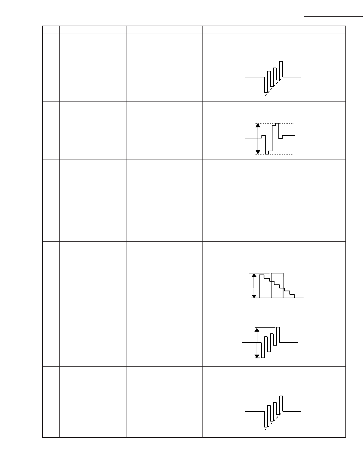
(4) Component 15 kHz signal adjustment
Item Adjusting conditions/points Adjusting procedure
1 Signal setting Signal: Provide the 100% color bar source of component 15k
Component 15k to the component input pin of video input 1.
100% color bar
Signal pin:
INPUT1 COMPONENT
2 COMP 15K GAIN Page: 5 Adjust "COMP 15K GAIN" so that
Location: Pin (1) of P801 0.70 ± 0.01 Vp-p is achieved at pin (1) of P801.
3 COMP 15K CB GAIN Page: 5 Adjust "COMP 15K CB GAIN" so that the width
Location: Pin (3) of P801 shown below is 0.70 ± 0.01 Vp-p at pin (3) of P801.
4 COMP 15K CR GAIN Page: 5 Adjust "COMP 15K CR GAIN" so that the width
Location: Pin (5) of P801 shown below is 0.70 ± 0.01 Vp-p at pin (5) of P801.
(5) Component HDTV signal adjustment
Item Adjusting conditions/points Adjusting procedure
1 Signal setting Signal: Provide the component HDTV source of the 100%
Component HDTV color bar to the component pin of video input 1.
100% color bar
Signal pin:
INPUT1 COMPONENT
2 COMP HDTV Page: 6 Adjust "COMP HDTV CONTRAST" so that the
CONTRAST Adjustment Location: Pin (9) of P801 difference between the black and while peaks is 0.95
± 0.02 Vp-p at pin (9) of P801.
28
Page 29

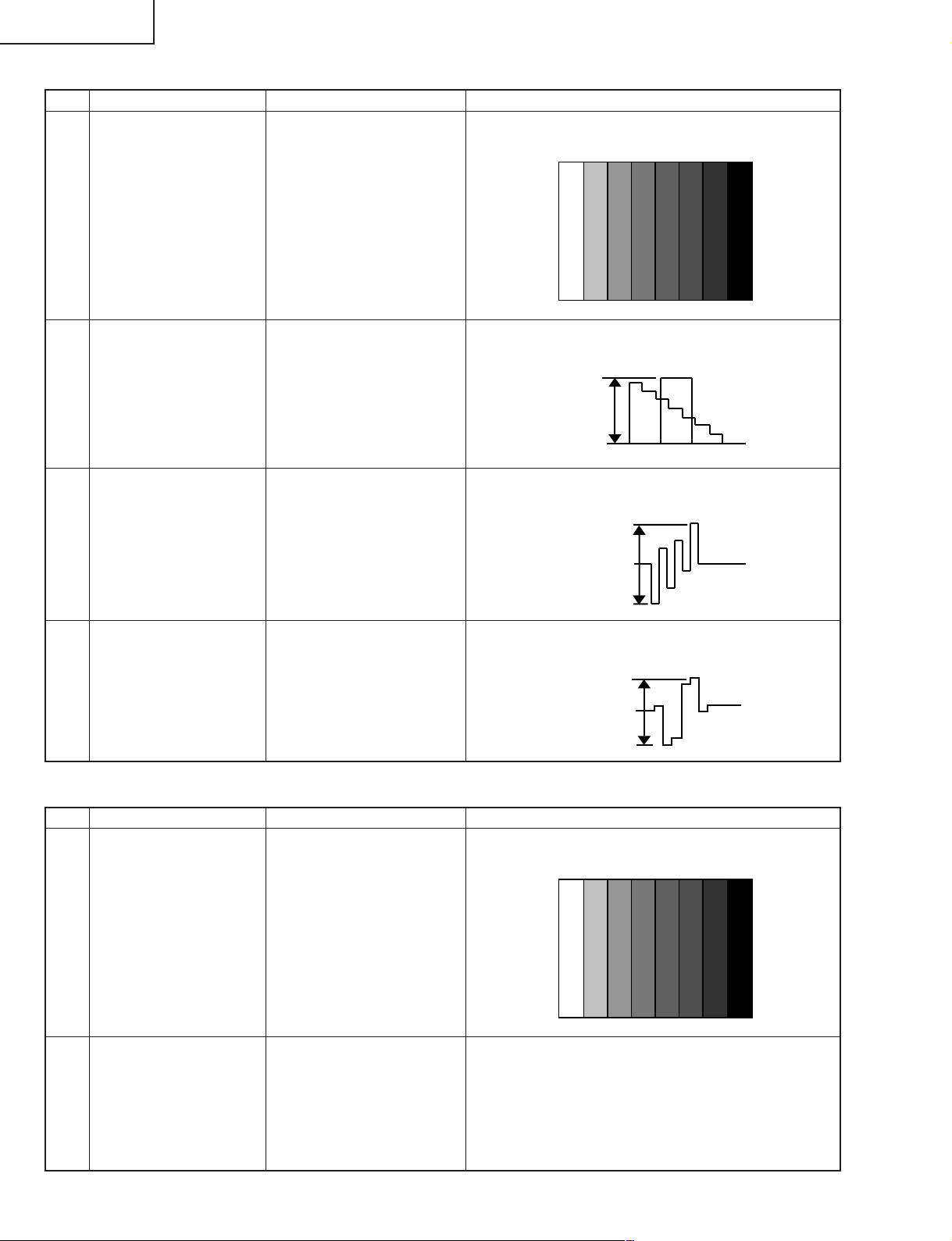
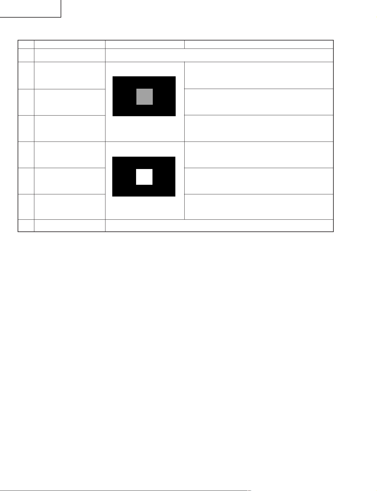
2) Digital white balance adjustment
(1) NTSC signal adjustment
Item Adjusting conditions Adjusting procedure
1 Setting
2
N358 R cutoff
N358 G cutoff
3
N358 B cutoff
4
N358 R drive
5
N358 G drive
6
N358 B drive
7
8 Convergence
LC-37HV6U
1. Provide the adjusting N358 signal (adjustment conditions) to the video image input pin of
video input 1. Page: 8
20% white window pattern
~
It is recommended that a
pattern without chroma and
burst be used.
80% white window pattern
~
It is recommended that a
pattern without chroma and
burst be used.
Repeat the above adjustments until convergence is reached (Adjust cutoff, drive, cutoff, drive and so on.)
1. Press "1" on the remote controller in the process
adjustment mode.
2. Adjust "N358 R CUTOFF" so that the luminance level of
the window pattern is maximized.
1. Press "2" on the remote controller in the process
adjustment mode.
2. Adjust N358 G CUTOFF so that the luminance level of
the window pattern is maximized.
1. Press "3" on the remote controller in the process
adjustment mode.
2. Adjust "N358 B CUTOFF" so that the luminance level of
the window pattern is maximized.
1. Press "4" on the remote controller in the process
adjustment mode.
2. Adjust "N358 R DRIVE" so that the luminance level of
the window pattern is maximized.
1. Press "5" on the remote controller in the process
adjustment mode.
2. Adjust "N358 G DRIVE" so that the luminance level of
the window pattern is maximized.
1. Press "6" on the remote controller in the process
adjustment mode.
2. Adjust "N358 B DRIVE" so that the luminance level of
the window pattern is maximized.
(2) COMPONENT 15 kHz signal adjustment
Item Adjusting conditions Adjusting procedure
1 Setting
2
COMP 15 kHz
R cutoff
COMP15 kHz
3
1. Provide the adjusting 525i component signal (adjustment conditions) to the component
video input pin of video 1. Page: 9
20% white window pattern
G cutoff
COMP 15 kHz
4
~
Simply press Y.
80% white window pattern
5
B cutoff
COMP
15 kHz
R drive
COMP15 kHz
6
G drive
COMP 15 kHz
7
~
B drive
Simply press Y.
1. Press "1" on the remote controller in the process
adjustment mode.
2. Adjust "COMP 15K R CUTOFF" so that the luminance
level of the window pattern is maximized.
1. Press "2" on the remote controller in the process
adjustment mode.
2. Adjust "COMP 15K G CUTOFF" so that the luminance
level of the window pattern is maximized.
1. Press "3" on the remote controller in the process
adjustment mode.
2. Adjust "COMP 15K B CUTOFF" so that the luminance
level of the window pattern is maximized.
1. Press "4" on the remote controller in the process
adjustment mode.
2. Adjust "COMP 15K R DRIVE" so that the luminance
level of the window pattern is maximized.
1. Press "5" on the remote controller in the process
adjustment mode.
2. Adjust "COMP 15K G DRIVE" so that the luminance
level of the window pattern is maximized.
1. Press "6" on the remote controller in the process
adjustment mode.
2. Adjust "COMP 15K B DRIVE" so that the luminance
level of the window pattern is maximized.
8 Convergence
Repeat the above adjustments until convergence is reached (Adjust cutoff, drive, cutoff, drive and so on.)
29
Page 30
LC-37HV6U
(3) COMPONENT HDTV signal adjustment
Item Adjusting conditions Adjusting procedure
1 Setting
2
COMP HDTV
R cutoff
HDTVG cutoff
COMP
3
COMP HDTV
4
B cutoff
COMP HDTV
5
R drive
HDTV
COMP
6
G drive
HDTV
COMP
7
B drive
1. Provide the adjusting 1080i component signal (adjustment conditions) to the component
vide input pin of video 1. Page: 10
20% white window pattern
~
Simply press Y.
80% white window pattern
~
Simply press Y.
1. Press "1" on the remote controller in the process
adjustment mode.
2. Adjust "COMP HDTV R CUTOFF" so that the
luminance level of the window pattern is maximized.
1. Press "2" on the remote controller in the process
adjustment mode.
2. Adjust "COMP 15K G CUTOFF" so that the luminance
level of the window pattern is maximized.
1. Press "3" on the remote controller in the process
adjustment mode.
2. Adjust "COMP HDTV B CUTOFF" so that the luminance
level of the window pattern is maximized.
1. Press "4" on the remote controller in the process
adjustment mode.
2. Adjust "COMP HDTV R DRIVE" so that the luminance
level of the window pattern is maximized.
1. Press "5" on the remote controller in the process
adjustment mode.
2. Adjust "COMP HDTV G DRIVE" so that the luminance
level of the window pattern is maximized.
1. Press "6" on the remote controller in the process
adjustment mode.
2. Adjust "COMP HDTV B DRIVE" so that the luminance
level of the window pattern is maximized.
8 Convergence
Repeat the above adjustments until convergence is reached (Adjust cutoff, drive, cutoff, drive and so on.)
30
Page 31

LC-37HV6U
4. Factory setting
Item Adjusting conditions Adjusting procedure
INDUSTRY INIT
1
Page: 1
Notes:
1) Perform factory setting as the latest task. Do not turn on the power after factory setting.
2) Turn the AVC’s AC power off to turn off the system.
Never turn off the power during factory setting.
3) After completion of factory setting, the system will exit from the process adjustment mode automatically. If not so,
HDCP has been set to off. Check HDCP setting.
4) Factory setting results in initializations of all user settings including channel setting.
(Items set in process adjustment mode are not initialized).
Items initialized by factory setting include the following:
• User settings (menu)
• Channel data (including broadcast frequencies)
• Password
• Operation time
• Auto installation flag
• Optimal manufacturer settings
• VCHIP block setting
1. Move the cursor to the "INDUSTRY INIT" line, use the
VOL key to turn the system on and press the ENTER
key.
Factory setting is complete when the process adjustment
menu disappears and the system enters the TUNER
input mode.
~Make sure HDCP is on. If it is off, the system cannot
exit from the process adjustment mode.
2. Turn off the AVC AC power.
31
Page 32

LC-37HV6U
Ë Ë
Ë Adjustment Model Menu List (AVC System)
Ë Ë
Do not change items, the adjustment procedure of which is not described in this manual. Inadvertent changes of
such items may result in unexpected or unrecoverable errors.
PAGE LINE NAME FUNCTION
1 1 KEY WRITE
2 INDUSTRY INIT Resetting the internally stored data to the factory settings
3 CENTER Version Main microprocessor version information (program)
4 OSD Version Main microprocessor version information (data)
5 CVIC Version Main microprocessor version information (program)
6 MONITOR Version Monitor microprocessor version information
7 ModelSelect MAIN
8 ModelSelect AV
9 ModelSelect MONITOR
10 STANDBY TYPE
11 HOTEL MODE
2 1 Ë+BAdj3.3V 3.3V adjustment
3 1 ËN358 MAIN Adjust
4 1 ËN358 SUB Adjust
5 1 ËCOMP 15K Adjust
6 1 ËCOMP HDTV Adjust
7 1 TUNER TEST1(CH15)
8 1 ËN358 White Balance
9 1 ËCOMP15K White Balance
2 Ë+BAdj1.8V(Enter:Auto)
3 ËREFERENCE Adjust
4 Select Adj Signal
5 Center Acutime Cumulative operating time on AVC center side
6 RESET Reset
7 BackLight Acutime Cumulative operating time of monitor
8 RESET Reset
2 N358 MAIN+SUB Adjust
3 MAIN N358 Y GAIN Adjustment in one-screen mode or adjustment of main side (left) in two-screen mode
4 MAIN N358 CB GAIN Adjustment in one-screen mode or adjustment of main side (left) in two-screen mode
5 MAIN N358 CR GAIN Adjustment in one-screen mode or adjustment of main side (left) in two-screen mode
6 MAIN N358 TINT Adjustment in one-screen mode or adjustment of main side (left) in two-screen mode
7 MAIN CONTRAST 15K Adjustment in one-screen mode or adjustment of main side (left) in two-screen mode
8 MAIN CUBBRIGHT 15K
2 SUB N358 CONTRAST Adjustment of sub side (left side) in two-screen mode
3 SUB N358 COLOR GAIN Adjustment of sub side (left side) in two-screen mode
4 SUB N358 TINT Adjustment of sub side (left side) in two-screen mode
5 TUNERA DAC ADJ Level adjustment of Tuner-A
6 TUNERB DAC ADJ Level adjustment of Tuner-B
2 COMP 15K GAIN Adjustment of component (480i)
3 COMP 15K CB GAIN Adjustment of component (480i)
4 COMP 15K CR GAIN Adjustment of component (480i)
2 COMP HDTV CONTRAST Adjustment of component (1080i)
3 COMP HDTV SUBBRIGHT Adjustment of component (1080i)
2 TUNER TEST2(CH10)
3 PEAK ACL SW
4 DC TRAN
5 DYNAMIC GAMMA
6 SIGNAL INFO
7 CENTER PROG UPDATE Version upgrade of software
8 EEPROM SAVE Adjustment value data save
9 EEPROM RECOVER Adjustment value data recovery
2 PAL White Balance
3 PC White Balance
4 N358 R CUTOFF White balance adjustment of NTSC
5 N358 G CUTOFF White balance adjustment of NTSC
6 N358 B CUTOFF White balance adjustment of NTSC
7 N358 R DRIVE White balance adjustment of NTSC
8 N358 G DRIVE White balance adjustment of NTSC
9 N358 B DRIVE White balance adjustment of NTSC
2 COMP15K R CUTOFF Digital white balance adjustment of component (480i)
3 COMP15K G CUTOFF Digital white balance adjustment of component (480i)
4 COMP15K B CUTOFF Digital white balance adjustment of component (480i)
5 COMP15K R DRIVE Digital white balance adjustment of component (480i)
6 COMP15K G DRIVE Digital white balance adjustment of component (480i)
7 COMP15K B DRIVE Digital white balance adjustment of component (480i)
8 COMP15K PASS SW
1.8V adjustment (Note that the value measured at the terminal area of the PC/IF PWB unit is 1.9V.)
32
Page 33

PAGE LINE NAME FUNCTION
10 1 ËCOMP33K White Balance
2 COMPHDTV R CUTOFF Digital white balance adjustment of component (1080i)
3 COMPHDTV G CUTOFF Digital white balance adjustment of component (1080i)
4 COMPHDTV B CUTOFF Digital white balance adjustment of component (1080i)
5 COMPHDTV R DRIVE Digital white balance adjustment of component (1080i)
6 COMPHDTV G DRIVE Digital white balance adjustment of component (1080i)
7 COMPHDTV B DRIVE Digital white balance adjustment of component (1080i)
11 Omitted
12 1
13 1 DEBUG PRINT SW
MONITOR GAMMA OFFSET R
2
MONITOR GAMMA OFFSET G
3
MONITOR GAMMA OFFSET B
4 MONITOR GAMMA R
5 MONITOR GAMMA G
6 MONITOR GAMMA B
7 MONITOR GAMMA WRITE
2 PIC ADJ MAKER SELECT
3 PIC ADJ KOUTEI SELECT
4 1274 V_CD_MODE
5 ACL HARD SW
6 DEBUG_SELECT_SW
7
DEBUG COMPANY SELECT
8
DEBUG PANELTYPE SELECT
LC-37HV6U
33
Page 34

LC-37HV6U
UPGRADING INSTALLED PROGRAMS
Programs installed in the product are mainly divided into the following two categories:
∫ Main programs (for AVC System)
∫ Monitor program (for Display)
CAUTON: Exercise great care to hide the procedure in entering the in-process adjustment mode from the
customer. Inadvertent setting changes in this mode may cause a fatal error resulting in a program being
unrecoverable.
[Tools required]
∫ PC
A Windows 95/98/me/2000/XP PC that has a COM port (RS-232C).
A USB-R232C converter will be acceptable provided that it is appropriately set and has PC compatibility.
∫ RS-232C cross cable
Interlink cable is also acceptable.
[Preparations]
Rewriting a program needs the product to enter the adjustment process mode.
1) The re writing software is supplied in the form of an ex e file named e.g., "MAIN_2002_10_10A.e x e" (provisional).
Create a directory on a HD and copy the software into the directory.
2)Double-click the file. The file will be self-extracted. Check the extracted file against the documentation
accompanying with the software.
3) Connect the AVC System and the Display unit with each other and make them ready for oper ation (mak e sure
the power LEDs of the AVC System and Display unit turn red).
4) Use an RS-232C cable to connect the PC to the AVC System.
5) Exercise great care to hide the procedure in entering the adjustment process mode from the customer.
Press the "MAIN POWER" button while holding down the "VOL (–)" key and the "INPUT" key on the Display
unit simultaneously.
If blue characters appear on the display, the system has entered the in-process adjustment mode successfully.
If not (the normal activation screen opens), retry.
[Rewriting the main program]
1) In the in-process adjustment mode , press the "CH(ù)" k e y on the remote controller. You will move to page ("7"
will appear on the upper left corner of the screen).
2) Make sure CENTER PROG UPDATE on page 7 is highlighted.
(It checks that "CENTER PROG UPDATE" on page 7 is chosen.)
3) Use the "VOL(–)/(+)" keys to change OFF to ON.
4)Press the "ENTER" key on the remote controller. Characters on the screen will disappear and the screen
blacks out.
5) Double-click the batch file specified in the document accompanying with the software.
6) A black window (MS-DOS window) will open and rewriting starts automatically.
Rewiring of the main program is now complete. Unplug the AC cord from the AVC System and turn off the
system and then on again.
7) Enter the adjustment process mode and make sure the version information on the CENTER Version, OSD
Version and CVIC Version lines on page 1/13 has been updated.
34
Page 35

LC-37HV6U
Continued
35
Page 36

LC-37HV6U
[How to rewrite the monitor program]
1) After entering the process adjustment mode, start up the terminal software obtained separately.
(Freeware products available on the Internet can be used.)
2) Make setting as shown below.
Baud rate: 9600
Data: 8 bits
Parity: NONE
Stop: 1 bit
Flow control: NONE
3) If the above setting is made correctly, pressing the "ENTER" key on the PC will make "ERR" appear on the
terminal software.
4) In this state, type the following. (
The characters displayed on the screen disappear and the screen becomes black.
IPL_0002
~ Immediately after the above entry, an unusual display may be appear on the terminal software, which means no
abnormal condition.
5) Change the baud rate to 115200.
6) Press the "ENTER" key to make appear the following display
ERR
SEND "MONITOR PROG UPDATE PROGRAM" from PC to MR
7) Using the file transmission function (function to transmit specified file contents) of the terminal software, select
the decompressed file (specified by the attached documentation) in the directory on the PC and execute
transmission.
8) When the following display appears on the terminal software, rewriting of the monitor program has been
completed. (Its contents may vary depending on the terminal software or program.)
Unplug the power cord to turn off the power and then turn it on again.
9) For confirmation, enter the process adjustment mode again and check that the version information shown on
the line "Monitor Version" on the 1st page corresponds to the new version shown on the attached documentation.
means the ENTER key.)
36
Page 37

LC-37HV6U
ADJUSTMENT PROCEDURES (Displa y)
The adjustment values are set to the optimum conditions at the factory before shipping. If a value should become
improper or an adjustment is required due to part replacement, make an adjustment according to the following
procedure.
1. Preparation
Note that the unit should be replaced when the receiver IC (IC2206), HDCP key R OM (IC2208) or microprocessor
(IC2004) is replaced.
Applicable unit: DKEYHC016FE53
2. Adjusting procedure
Entering the adjustment process mode → VLS BIAS (15V) voltage adjustment → GRAY LEVEL (14.5V) voltage
adjustment → COM BIAS adjustment → Background adjustment
3. How to enter the adjustment process mode
(1) When the AVC System is not connected
• Turn OFF the monitor main power. Turning ON the monitor main power while pressing the "INPUT" key
and "VOL (–)" ke y on the top face of the monitor main body together will establish the "Monitor Process"
mode.
(2) When the AVC System is connected
• Turn OFF the monitor main power. Turning ON the monitor main power while pressing the "CH (Ù)" key
and "VOL (+)" key on the top face of the monitor main body together will establish "Monitor Process"
mode.
In each case of (1) and (2), "<K>" is displayed in the upper left portion of the screen.
Then, pressing any key will bring you to the first page of the "Monitor Adjustment" mode.
~ To exit the adjustment process mode, turn OFF the main power.
4. Adjustment process mode key operation table
Key
Cursor UP
Cursor DOWN
Cursor RIGHT
Cursor LEFT
ENTER
INPUT
CH (ù)
CH (Ù)
VOL (+)
VOL (–)
Function 1 (when on the left side of a page)
Moving up by one item or moving to the
previous page (when at the top)
Moving down by one item or moving to the next
page (when at the bottom)
Moving to the right by one item or moving to
another page (in the case of the initial page)
Moving to the left by one item or moving to
another page (in the case of the initial page)
Test pattern off
Moving to the next page
Moving down by one item or moving to the next
page (when at the bottom)
Moving down by one item or moving to the next
page (when at the bottom)
Moving to the right by one item or moving to
another page (in the case of the initial page)
Moving to the left by one item or moving to
another page (in the case of the initial page)
Function 2 (when changing a numeric value)
Incrementing the adjustment value by one or
executing the item (in the case of W or R items)
Decrementing the adjustment value by one or
executing the item (in the case of W or R items)
Moving to the right by one item
Moving to the left by one item
Executing the item (in the case of W or R
items)
Moving to the next page
Incrementing the adjustment value by one or
executing the item (in the case of W or R items)
Decrementing the adjustment value by one or
executing the item (in the case of W or R items)
Moving to the right by one item
Moving to the left by one item
37
Page 38

LC-37HV6U
5. Adjustment
5-1.VLS BIAS (15V) voltage adjustment
5-2.GRAY LEVEL (14.5V) voltage adjustment
5-3.COM BIAS adjustment
5-4.Background adjustment
Shift to the "VLS BIAS" item with the cursor UP/DOWN key and select a numeric value with the cursor
RIGHT/LEFT key.
Connect a digital volt meter to TP4101 (or C4180+) on the monitor PWB and make a adjustment with the
cursor UP/DOWN key so that the voltage becomes 15.00V±0.05V.
Shift to the "GRAY LEVEL" item with the cursor UP/DOWN key and select a numeric value with the cursor
RIGHT/LEFT key.
Connect a digital volt meter to TP4104 (near IC4105) on the monitor PWB and mak e a adjustment with the
cursor UP/DOWN key so that the voltage becomes 14.50V±0.05V.
Because this voltage is a gray scale reference voltage, adjust it correctly.
Shift to the "COM BIAS" item with the cursor UP/DOWN key and select a numeric value with the cursor
RIGHT/LEFT key.
Changing the numeric value with the cursor UP/DOWN key will make appear the test patter n. Make an
adjustment so that the flicker near the center of the screen is minimized.
Start up the set with the AVC System connected and adjust the background of the monitor.
• Procedure
-1) Display the adjustment screen (200-level gray scale on High side, 48-level gray scale on Low side).
-2) Adjust "R OFFSET", "G OFFSET" and "B OFFSET" so that the 200-level gr ay scale pattern becomes
normative.
Adjust the chromaticity of the High pattern (in the left portion of the screen) so that x = 0.287 and y =
0.302.
-3) Adjust "R GAMMA", "G GAMMA" and "B GAMMA" so that the 48-level gray scale pattern becomes
normative.
Adjust the chromaticity of the Low pattern (in the right portion of the screen) so that x = 0.275 and y
= 0.280.
The above-mentioned adjustments can be made according to the following procedure.
38
Page 39

LC-37HV6U
(1) Adjusting method using RS-232C
• Get a personal computer with a COM port (RS-232C) equipped with WINDOWS 95/98/me/2000/xp and
a RS-232C crossing cable
• Start up the set with the RS-232C cable connected.
• Start up the terminal software.
(Freeware products available on the Internet can be used.)
• Make setting as shown below.
Baud rate : 9600
Data : 8 bits
Parity : None
Stop : 1 bit
Flow control : None
• If the above setting is made correctly, pressing the "ENTER" key on the PC will make "ERR" appear on
the terminal software.
• In this state, entering a command shown in the table bellow and pressing the "ENTER" key will allow y ou
to make an adjustment.
If "OK" is displayed on the terminal software after the "ENTER" key is pressed, the command has been
entered successfully.
If "ERR" is displayed, enter the command again.
RS232C command table
Command
MSET1001
MOFR~~~~
MOFG~~~~
MOFB~~~~
MGAR~~~~
MGAG~~~~
MGAB~~~~
MINF0000
MINF0001
MINF0002
Function
Used to start the background adjustment.
Used to adjust the value of R OFFSET.
Used to adjust the value of G OFFSET.
Used to adjust the value of B OFFSET.
Used to adjust the value of R GAMMA.
Used to adjust the value of G GAMMA.
Used to adjust the value of B GAMMA.
Used to display the R GAMMA table.
Used to display the B GAMMA table.
Used to display the G GAMMA table.
Remarks
The adjustment ends with a numeric value other than 1001.
Range: 0000 to 0512 (Initial value: 0255)
Range: 0000 to 0512 (Initial value: 0255)
Range: 0000 to 0512 (Initial value: 0255)
Range: 0000 to 0255 (Initial value: 0100)
Range: 0000 to 0255 (Initial value: 0100)
Range: 0000 to 0255 (Initial value: 0100)
39
Page 40

LC-37HV6U
Lamp error detection
1. Feature description
This liquid-crystal TV incorporates a lamp error detection feature (lamp error detection) that automatically
turns OFF the power for safety under abnormal lamp or lamp circuit conditions.
If anything is wrong with the lamp or lamp circuit or the lamp error detection feature is activated for some
reason, the following will result.
1 The power of TV main body is turned OFF about 13 seconds after it is turned ON. (The power LED on
2 If 1 occurs five times consecutively, it becomes impossible to turn ON the power. (The power LED
2. Measures
2-1.Checking with lamp error detection OFF
Disconnect the cable connected to the AVC System Turn OFF the monitor main power. Turning ON the
monitor main power while pressing the "INPUT" key and "VOL (–)" key together will establish the "Monitor
Process" mode ("<K>" is displayed).
Then, pressing any key will bring you to the first page of the "Monitor Process" mode.
This allow you to check the lamp and lamp circuit for abnormal conditions.
Check that "L ERR RESET" on the fourth line of the first page of the "Monitor Process" mode is 1 or more.
If it is 1 or more, a lamp error has been detected.
2-2.Reset of lamp error count
After checking the lamp and lamp circuit for abnormal conditions, reset the lamp error count. Move the
arrow to "L ERR RESET" on the fourth line of the first page of the "Monitor Process" mode with the cursor
UP/DOWN ke y and select the numeric value of "L ERR RESET" with the cursor RIGHT/LEFT key. In this
state, press the cursor UP/DOWN key to reset it to "0".
the front of the TV turns red from green and keeps blinking in red (ON for 250ms and OFF for 1sec).)
keeps blinking in red (ON for 250ms and OFF for 1sec).)
First page of monitor process mode
SERVICE
GRAYLEVEL
COMBIAS
VLSBIAS
→L ERR RESET
LCD
PATTERN
SOUND AND FAN
OTHER
VER M1.~~ CEEP8
Then perform operation checking and check that the lamp error detection feature is not activated.
37AD1
076
077
064
5
Values specific to each monitor
Resetting to "0"
40
Page 41

•List of process adjustment modes (Display)
LC-37HV6U
41
Page 42

LC-37HV6U
Process adjustment list
1st level Page Item Setting range Initial value
Contents 0 GRAYLEVEL 0~255 112
COM BIAS 0~255 87
VLS BIAS 0~255 41
L ERR RESET Zero clear 0
LCD 1 MODE 50Hz, 60Hz, PC 60Hz
PWM CTRL 0~7 7
PWM FREQ 0~4095 1289
PWM DUTY1 0~4095 0
PWM DUTY2 0~4095 0
PHASDIF 0~255 0
PCLK1 0~3 0
PCLK2 0~7 0
2 MODE 50Hz, 60Hz, PC 60Hz
OS SW 0~1 0
OS D1 0~255 110
OS D2 0~255 123
OS D3 0~255 135
OS D4 0~255 155
OS D5 0~255 167
OS D6 0~255 174
OS D7 0~255 179
3 MODE 50Hz, 60Hz, PC 60Hz
OPC 0 0~85 00
OPC 1 0~85 20
OPC 2 0~85 29
OPC 3 0~85 38
OPC 4 0~85 47
OPC 5 0~85 56
OPC 6 0~85 65
OPC 7 0~85 75
4 MODE 50Hz, 60Hz, PC 60Hz
OPC 8 0~85 85
OS AUTO 0~1 0
PATTERN 1 PATTERN1 0~14 0
PATTERN2 0~12 0
R GAMMA 20~180 Display only 100
R OFFSET 0~510 Display only 255
G GAMMA 20~180 Display only 100
G OFFSET 0~510 Display only 255
B GAMMA 20~180 Display only 100
B OFFSET 0~510 Display only 255
SOUND 1 100HZ 0~255 92
400HZ 0~255 96
1KHZ 0~255 145
4KHZ 0~255 187
10KHZ 0~255 187
FAN START 0~255 224
FAN END 0~255 230
TEMP ERR 0~255 55
OTHER 1 CLR MODE 1 digit 0~4 0
W –
LCD DATA 4 digits 0~F –
R/W –
EEPROM 7 digits 0~F –
R/W –
SII861 6 digits 0~F –
R/W –
2 L ERR STOP 0~1 0
MODE 0~4 0
REMOCON 0~1 0
OSTEMP AD 0~255 AD value
OPC AD 0~255 AD value
42
Page 43
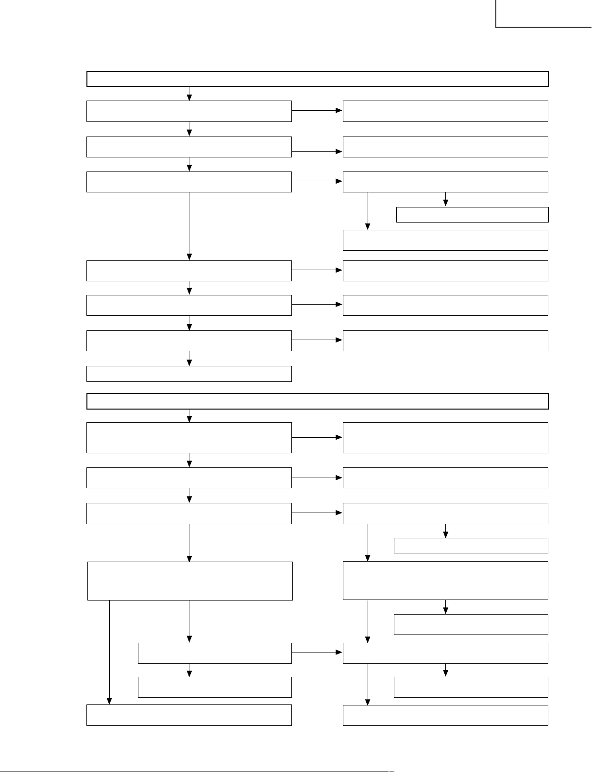
AVC System
LC-37HV6U
TROUBLE SHOOTING TABLE
Power is not supplied. (The front LED does not come on.)
Is the power cord connector connected to the main body
correctly?
YES
Is the fuse (F701) normal?
YES
Is the BU+5V line (pin (9) of P1702) normal?
YES
Are the wire harness, FFC, etc. in the set connected
correctly?
YES
Are there voltage variations on the OVP line (pin (3) of
P1702) just after the power is turned ON?
YES
Are each DC/DC converter output and MOS-FET (Q1701,
Q1702, Q1703 and IC1706) normal?
YES
Replace IC1702.
NO
NO
NO
NO
NO
NO
Connect the power cord correctly and turn ON the power
SW.
Replace the fuse. If the fuse blows when the power SW is turned
ON, replace D701 and IC 701 and perform checking again.
Is there any faulty part or short-circuited circuit on the
BU+5V line?
YES
Check the peripheral circuitry of IC1701.
Remove the faulty or short-circuited part and perform
checking again.
Connect the wire harness, FFC, etc. in the set correctly and
perform checking again.
Check the parts (IC701, IC721, PC702, Q702, Q703 and
D711) in the power unit.
Check each DC/DC converter output and replace MOS-FET
(Q1701, Q1702, Q1703 and IC1706).
NO
Power is not supplied in spite of power-on operation being performed. (The front LED does not turn green from red or blinks in red.)
Are the connectors MDR (white) and DVI (gray) of the
system cable connecting the Display and AVC System
connected correctly?
YES
Are the power SW on the AVC System side and the power
SW on the Display side turned ON?
YES
Are the voltages on the UR+6V, UR+10V and UR+13V
lines (pins (13), (1) and (17) of P1702) normal?
YES
Are the D+1.8VCV (pins (5) and (6) of P1701), D+3.3V (pin
8 of P1701) line, A+5V (pin 3 of P1701) and D+5V (pin (1)
of P1701) normal?
YES
Is D_POW (pins (32), (33) and (34) of IC1702, pin
(2) of IC1704 and pin (2) of IC1705) set to "H"?
Check the line of D_POW (pin (6) of main
PWB IC1503).
NO
NO
NO
NO
NO
YES
Connect the connectors correctly and turn ON the power
again.
Turn ON the power SW on the AVC System side and the
power SW on the Display side and turn ON the power.
Is PS_ON (pin (11) of P1702) set to "H" (3.5V)?
YES
Are the impedances of the UR+6V, UR+10V and UR+13V
lines normal?
(Measure the resistances between pins (13), (1) and (17) of
P1702 and GND.)
YES
Check the UR+6V, UR+10V and UR+13V
lines and the circuit parts on the lines.
Are MOS-FET (Q1701, Q1702 and Q1703 and REG IC
(IC1704 and IC1705) normal?
NO
NO
Check the PS_ON line.
NO
YES
Replace IC1702.
Check if the wire harness, FFC, etc. in the set are
connected correctly.
Check each output line and replace MOS-FET (Q1701, Q1702
and Q1703 and REG IC (IC1704 and IC1705).
43
Page 44

LC-37HV6U
YES
YES
YES
YES
NO
NO
NO
NO
No sound comes out. (Sounds come out at the time of TV broadcast receiving.)
No sound comes out from the headphones.
Check or replace the peripheral circuitry of IC2501.
No sound comes out from the monitor
Perform checking from pins (25) and (24) of
IC2501 to L.P.F (IC2506), H/P AMP (IC2502) and
audio mute (Q2501) and around the headphone
terminal. Are they all as specified?
Is the audio output from the monitor output
set to "Variable"? Are the headphones
connected?
Check the headphone mute circuit.
(Check the peripheral circuitry of D2501,
Q2501 and IC2502.)
Is the audio output from IC2501 (MULTI
SOUND PROCESSOR) normal?
Pins (34) and (33) of IC2501 (SC2 OUT L/R)
Check the headphone plug circuit.
Perform checking from pin (6) of headphone
(J2402) to pin (30) of IC1601. Are they all
as specified?
Perform checking from pins (34) and (33) of
IC2501 to pins (16) and (10) of the monitor
output terminal (J1104).
Check IC2504, Q2503 and Q2502 as well
as audio mute circuit (Q1103 and Q1102).
NO
YES
YES
YES
YES
YES
NO
NO
NO
No sound comes out at the time of TV broadcast receiving. (Sounds come out at the time of external input.)
No sound comes out at the time of UHF/VHF receiving.
Is the input signal to pin (67) (SOUND 1F1) and pin (69) (SOUND 1F2) of IC2501 (MULTI SOUND
PROCESSOR) normal?
Check B.P.F. of SIF1 and SIF2. Are they all
as specified?
Is the SIF output from the tuner normal?
(Pin (7) of TU1101 and pin (7) of TU1102)
Check TU1101 and TU1102 (U/V tuner) and
the parts around them.
Is the I2S_DAOUT signal inputted normally from
pin (6) of IC2501 (MULTI SOUND
PROCESSOR) to pin (25) (SDI0) of IC2518?
Check if the I2S_DAOUT, I2S_CL, I2S_WS and
I2S_DAIN signals are outputted from IC2501 and
inputted to IC2518 (DSP).
Is the audio output from IC2501 (MULTI
SOUND PROCESSOR) normal?
Pins (28) and (27) (DAC_M L/R) of IC2501
Check IC2501 (MULTI SOUND
PROCESSOR) and the peripheral circuitry.
Is the audio output from pins (7) and (1) of
IC2505 (OP_AMP) normal?
Check the display side.
Check the peripheral circuitry of IC2505
(OP_AMP).
NO
YES
YES
No sound comes out at the time of external input and PC input. (Sounds come out at the time of TV broadcast receiving.)
Is the audio input signal to IC1301 (AV
SWITCH) normal?
<INPUT1>
Pin(24) fo IC1301 (L/R VIDEO1)
<INPUT2>
Pin(9) and (11) IC1301 (L/R VIDEO2)
<INPUT3>
Pin(16) and (18) IC1301 (L/R VIDEO3
<INPUT4>
Pin(23) and (25) IC1301 (L/R VIDEO4)
<PC SOUND INPUT>
Pin(29) and (31) IC1301 (L/R PC-IN)
Check IC1301 (AV SWITCH) and the
peripheral circuitry.
Check IC2501 (MULTI SOUND
PROCESSOR) and the peripheral circuitry.
Are the audio input circuits of IC1301 (AV
SWITCH) normal?
Perform checking from pins (18) and (12) of J1103
to pins (2) and (4) (L/R VIDEO1) of IC1301.
Perform checking from pins (16) and (10) of J1103
to pins (9) and (11) (L/R VIDEO2) of IC1301.
Perform checking from pins (18) and (12) of J1104
to pins (16) and (18) (L/R VIDEO3) of IC1301.
Perform checking from pins (5) and (7) of J2404 to
pins (23) and (25) (L/R VIDEO4) of IC1301.
Perform checking from pins (2) and (3) of J2403 to
pins (29) and (31) (L/R PC-IN) of IC1301.
Is the audio output signal from IC1301 (AV
SWITCH) normal?
Pins (52) and (54) of IC1301
(LOUT1/ROUT1)
Is the audio input signal from IC2501(MULTI
SOUND PROCESSOR) normal?
Pin(56) and (57) of IC2501(SC1INL/R)
AVC System
44
Page 45
NO
NO
NO
NO
NO
NO
NO
NO
YES
YES
YES
YES
YES
YES
YES
YES
No picture comes out at the time of external input. (Pictures come out at the time of TV broadcast receiving.) <At the time
of CVBS video signal and S video signal input>
No external input picture comes out. <<INPUT 1 to 4>>
Is the desired INPUT mode selected on input change menu screen?
Select an input signal on the input signal source menu screen.
<At the time of CVBS video signal input> Is the video
signal inputted to pin (93) of IC7001 (MAIN Y/C
SEPARATOR)?
Perform checking from IC1301 to IC7001.
Are the Y, Cb and Cr MAIN signals inputted to pins
(69), (68) and (67) of IC803 (RGB DECODER)?
Perform checking from IC801 to IC803.
(Q842-4, IC813, IC814, Q814~816, etc.)
Are the Y, Cb and Cr MAIN signals outputted to pins
(21), (22) and (23) of IC801?
Check IC801 (MAIN VIDEO CHROMA) and the
peripheral circuitry.
Are the R, G and B MAIN signals outputted to pins (35),
(37) and (39) of IC803?
Check IC803 (RGB DECODER) and the peripheral
circuitry.
Are the R, G and B MAIN signals inputted to pins (25),
(1) and (5) of FL810 (30/6.7MHz L.P.F.)?
Perform checking from IC803 to FL810.
(Q801-3, etc.)
Are the R, G and B MAIN signals outputted to pins (17),
(14) and (11) of FL810?
Check PC I/F unit.
Cutoff frequency setting terminal (pin (21) of FL810
(6.7/30MHz L.P.F.))
〈〈525i〉〉: L
〈〈525P, 1125i and 750P
〉〉: H
<At the time of CVBS video signal input>
Are the MAIN-Y and MAIN-C signals inputted to pins
(41) and (39) of IC801 (MAIN VIDEO CHROMA),
respectively?
<At the time of Y/C video signal input>
Are the MAIN-Y and MAIN-C signals inputted to pins (44)
and (43) of IC801 (MAIN VIDEO CHROMA), respectively?
<At the time of CVBS video signal input>
Perform checking from IC1301 to IC801.
(Q7007, Q7008, IC7001, IC7003, Q7005, Q7006,
FL7004, FL7005, etc.)
<At the time of Y/C video signal input>
Perform checking from IC1301 to IC801.
(Q403, Q404, etc.)
NO
NO
NO
YES
NO
YES
YES
YES
YES
YES
YES
YES
YES
No TUNER (U/V) picture comes out.
Is the video signal outputted to the tuner
(TU1101/1102) output terminal (pin (17))?
Is the video signal inputted to pins (7) and (1) of IC1104
(LEVEL ADJ)?
Check IC1301 (AV SWITCH) and the peripheral
circuitry.
Check or replace the peripheral circuitry of the tuner
(TU1101/1102).
Is the video signal outputted to pins (5) and (3) of
IC1104 (LEVEL ADJ)?
Is the control signal for level adjustment inputted from
pins (1) and (2) of IC1105 to pins (6) and (2) of IC1104
(LEVEL ADJ)?
Is the tuner video input to IC1103 (AV SWITCH)
normal?
Pin (63) of IC1301 (MAIN TUNER IN)
Pin (60) of IC1301 (SUB TUNER IN)
Check or replace the peripheral circuitry of IC1105
(2CH_DA_CONV).
AVC System
<At the time of CVBS video signal input> Is the CVBS video signal outputted to pin (56) of IC1301?
<At the time of Y/C video signal input> Are the MAIN-Y, MAIN-C, SUB-Y and SUB-C signals outputted to pins (56), (58), (44) and
(47) of IC1301, respectively?
Is the signal inputted to each input terminal of IC1301 (AV SWITCH)?
<CVBS video signal input>
〈〈Input 1〉〉 Is the signal inputted to pin (1)? → Perform checking from pin (4) of J1103 to pin (1) of IC1301.
〈〈Input 2〉〉 Is the signal inputted to pin (8)? → Perform checking from pin (1) of J1103 to pin (8) of IC1301.
〈〈Input 3〉〉 Is the signal inputted to pin (15)? → Perform checking from pin (4) of J1104 to pin (15) of IC1301.
〈〈Input 4〉〉 Is the signal inputted to pin (22)? → Perform checking from pin (2) of J2404 to pin (22) of IC1301.
<S video signal input>
〈〈Input 1〉〉 Are the Y and C signals inputted to pins (3) and (5), respectively? → Perform checking from pins (9) and (10) of
SC1101 to pins (3) and (5) of IC1301.
〈〈Input 2〉〉 Are the Y and C signals inputted to pins (10) and (12), respectively? → Perform checking from pins (3) and (4) of
SC1101 to pins (10) and (12) of IC1301.
〈〈Input 3〉〉 Are the Y and C signals inputted to pins (17) and (19), respectively? → Perform checking from pins (9) and (10) of
SC1102 to pins (17) and (19) of IC1301.
〈〈Input 4〉〉 Are the Y and C signals inputted to pins (24) and (26), respectively? → Perform checking from pins (3) and (4) of
J2401 to pins (24) and (26) of IC1301.
〈〈MAIN system〉〉
NO
NO
NO
NO
NO
NO
<At the time of CVBS video signal input> Is the video
signal inputted to pin (7) of IC402 (SUB COMB
SEPARATOR)?
Perform checking from IC1301 to IC402.
Are Y, Cb and Cr SUB signals inputted to 6.7MHz
L.P.F. composed of Q901-6?
Perform checking from IC802 to Q901-6.
Are the Y, Cb and Cr MAIN signals outputted to pins
(21), (22) and (23) of IC802?
Check IC802 (SUB VIDEO CHROMA) and the
peripheral circuitry.
Are Y, Cb and Cr SUB signals outputted from 6.7MHz
L.P.F. composed of Q901-6?
Check Q901-6 (6.7MHz L.P.F.) and the peripheral
circuitry.
Check PC I/F unit.
<At the time of CVBS video signal input>
Are the MAIN-Y and MAIN-C signals inputted to pins
(1) and (48) of IC802 (SUB VIDEO CHROMA),
respectively?
<At the time of Y/C video signal input>
Are the MAIN-Y and MAIN-C signals inputted to pins (5)
and (7) of IC802 (SUB VIDEO CHROMA), respectively?
<At the time of CVBS video signal input>
Perform checking from IC1301 to IC802.
(Q407, Q408, IC402, IC404, Q416, Q417, Q418, etc.)
<At the time of Y/C video signal input>
Perform checking from IC1301 to IC802.
(Q409, Q410, etc.)
〈〈SUB system〉〉
LC-37HV6U
45
Page 46

LC-37HV6U
NO
NO
NO
YES
YES
YES
YES
No picture comes out at the time of external input. <At the time of COMPONENT video signal input>
No external input picture comes out.
〈〈INPUT 1/3〉〉
Is the desired INPUT mode selected on input change menu screen?
Select an input signal on the input signal source menu screen.
Is the signal inputted to pins (5), (7) and (9) of
IC1401 (AV SWITCH)?
→ Perform checking
from pins (7), (14) and (20) of J1103 to pins (5),
(7) and (9) of IC1401.
Is the signal inputted to pins (59), (61) and (63)
of IC1401 (AV SWITCH)?
→ Perform checking
from pins (7), (14) and (20) of J1103 to pins
(59), (61) and (63) of IC1401.
Is the signal inputted to pins (15), (17) and (19) of IC1401?
→ Perform checking from pins (20), (18) and (16) of IC1652 to pins (15),
(17) and (19) of IC1401.
Are the Y, Cb and Cr signals inputted to pins (26)
and (19), pins (25) and (18) and pins (27) and (17)
of IC801 (MAIN VIDEO CHROMA), respectively?
Perform checking from pins (50), (48) and (46) of
IC1401 to pins (26) and (19), pins (25) and (18)
and pins (27) and (17) of IC801.
Are the Y, Cb and Cr MAIN signals outputted to pins
(21), (22) and (23) of IC801, respectively?
Check IC801 (MAIN VIDEO CHROMA) and the
peripheral circuitry.
NO
NO
Are the R, G and B MAIN signals outputted to
pins (35), (37) and (39) of IC803, respectively?
Check IC803 (RGB DECODER) and the
peripheral circuitry.
NO
Are the R, G and B MAIN signals inputted to pins (25),
(1) and (5) of FL810 (6.7/30MHz L.P.F.), respectively?
Perform checking from IC803 to FL810. (Q801-
3, etc.)
Are the Y, Cb and Cr signals inputted to pins
(5) and (47), pins (4) and (48) and pins (3) and
(46) of IC803 (RGB DECODER), respectively?
Perform checking from pins (38), (36) and (34)
of IC1401 to pin (5), pins (47) and (4), pins (48)
and (3) and pin (46) of IC803.
Are the Y, Cb and Cr MAIN signals inputted to
pins (69), (68) and (67) of IC803 (RGB
DECODER), respectively?
Perform checking from IC801 to IC803.
(IC813, IC814, Q814-5, Q814-6, etc.)
NO
NO
NO
NO
YES
YES
YES
YES
YES
YES
YES
YES
Are the Y, Cb and Cr signals inputted to pins (19), (34),
(26) and (31), pins (18), (33) and (25) and pins (17), (35)
and (27) of IC802 (SUB VIDEO CHROMA), respectively?
Perform checking from pins (44), (42) and (40) of
IC1401 to pins (19), (34), (26) and (31), pins (18),
(33) and (25) and pins (17), (35) and (27) of IC802.
Are the Y, Cb and Cr SUB signals outputted to
pins (21), (22) and (23) of IC802, respectively?
Check IC802 (SUB VIDEO CHROMA) and the
peripheral circuitry.
Check the peripheral circuitry of Q901-2, Q903-
4 and Q905-6 (6.7MHz L.P.F.).
Are the Y, Cb and Cr SUB signals inputted to
Q901-2, Q903-4 and Q905-6 (6.7MHz L.P.F.),
respectively?
Are the R, G and B SUB signals outputted to
Q901-2, Q903-4 and Q905-6 (6.7MHz L.P.F.),
respectively?
Check the PC I/F unit.
Perform checking from IC802 to Q901-2, Q903-
4 and Q905-6 (6.7MHz L.P.F.).
NO
YES
YES
YES
YES
Are the R, G and B MAIN signals outputted to
pins (17), (14) and (11) of FL810, respectively?
Cutoff frequency setting terminal (pin (21) of
FL810 (6.7/30MHz L.P.F.))
〈〈525i〉〉: L
〈〈525P, 1125i and 750P
〉〉: H
NO
NO
No picture comes out at the time of external input. <At the time of DVI video signal input>
No external input picture comes out.
〈〈INPUT 3〉〉
Is the desired INPUT3 mode selected on input change menu screen?
Select a DVI signal on the input signal source menu screen.
Is the signal inputted to pins (52), (49), (51), (48), (6), (5), (2)
and (3) of IC1650 (DVI_D/A)?
→ Perform checking from
pins (9), (1), (10), (2), (24), (23), (18) and (17) of SC1650 to
pins (52), (49), (51), (48), (6), (5), (2) and (3) of IC1650.
Are the MAIN, PASS and SUB video signals outputted to pins (50), (48) and (46), pins (38), (36) and (34) and pins (44), (42) an
d (40) of IC1401, respectively?
Check IC1401 (AV SWITCH) and the peripheral circuitry.
Check the PC I/F unit.
Check IC1401 (AV SWITCH) and the peripheral circuitry.
AVC System
〈〈INPUT1〉〉 〈〈INPUT3〉〉
〈〈MAIN 525i system
〉〉
〈〈PASS 525P, 1125I and 750P system
〉〉
〈〈SUB system〉〉
Is the signal inputted to pins (8), (10) and (12)
of IC1652 (MULTI_PLEXER)?
→ Perform
checking from pins (31), (26) and (23) of
IC1650 to pins (8), (10) and (12) of IC1652.
Is the signal inputted to pins (1), (3) and (5) of
IC1652 (MULTI_PLEXER)?
→ Perform
checking from pins (25), (26) and (27) of
SC1650 to pins (1), (3) and (5) of IC1401.
〈〈Analog signal〉〉
〈〈Digital signal〉〉
46
Page 47

LC-37HV6U
NO
NO
NO
YES
YES
Unstable synchronization
Check the PC I/F unit.
Are HD1 and VD1 are outputted from pins
(9) and (4) of IC801 (MAIN VIDEO
CHROMA), respectively?
Check IC801 and the peripheral circuit.
Are HD1 and VD1 are inputted to pins (28)
and (27) of IC1901 (PLD), respectively?
Perform checking from pins (9) and (4) of
IC801 to pins (28) and (27) of IC1901.
Are HD3 and VD3 are outputted from pins
(7) and (6) of IC1901 (PLD), respectively?
Check IC1901 and the peripheral circuit.
NO
NO
YES
Are HD3 and VD3 are inputted to pins (14)
and (13) of IC604 (Sync. Sep.), respectively?
Perform checking from pins (7) and (6) of
IC1901 to pins (14) and (13) of IC604.
NO
NO
YES
YES
Are SP-HD, SP-VD and SP-CP inputted to
pins (5), (3) and (8) of IC1901,
respectively?
Perform checking from pins (16), (28) and
(15) of IC604 to pins (5), (3) and (8) of
IC1901.
Are PL-HD, PL-VD, PL-CP and PL-BLK
outputted from pins (30), (29), (31) and
(32) of IC1901, respectively?
Check IC1901 and the peripheral circuit.
NO
YES
Are Hsync, Vsync and SCP inputted to pins
(1) and (66), pins (2) and (65) and pin (31)
of IC803 (RGB DECODER), respectively?
Perform checking from pins (30), (29), (31)
and (32) of IC1901 to pins (1) and (66),
pins (2) and (65) and pin (31) of IC803.
NO
YES
YES
Are HS and VS outputted from pins (29)
and (28) of IC803?
Check IC803 and the peripheral circuit.
Are SP-HD, SP-VD and SP-CP outputted from
pins (16), (28) and (15) of IC604, respectively?
Check IC604 and the peripheral circuit.
YES
AVC System
〈〈NAIN system〉〉 (In the case of 15k)
NO
NO
NO
YES
YES
YES
Are HD2 and VD2 outputted from pins (9)
and (4) of IC802 (SUB VIDEO CHROMA),
respectively?
Check IC802 and the peripheral circuit.
Are HD2 and VD2 inputted to pins (41) and
(42) of IC1901 (PLD), respectively?
Perform checking from pins (9) and (4) of
IC802 to pins (41) and (42) of IC1901.
Are HDS and VDS outputted from pins (39)
and (40) of IC1901 (PLD), respectively?
Check IC1901 and the peripheral circuit.
〈〈SUB system〉〉
〈〈NAIN system〉〉
(In the case of D2, D3 and D4)
47
Page 48

LC-37HV6U
NO
YES
YES
YES
YES
YES
YES
YES
YES
No picture comes out.
No CC/TEXT comes out.
Is the desired CC/TEXT mode on menu screen?
Select the display mode with "CC" button of remote controller.
Is the input to pins (124),
(133) and (139) of IC10004
normal?
Check CN10006 and the
peripheral circuitry.
NO
Is the digital output section
of IC10004 normal?
Check IC10004 and the
peripheral circuitry.
NO
Is the digital output from
IC10025 normal?
Check IC10025 and the
peripheral circuitry.
NO
YES
YES
YES
Is the input to pins (126),
(136) and (141) of IC10004
normal?
Check CN10008 and the
peripheral circuitry.
NO
Is the digital output section
of IC10004 normal?
Check IC10004 and the
peripheral circuitry.
NO
Is the digital output from
IC10025 normal?
Check IC10025 and the
peripheral circuitry.
NO
YES
YES
YES
Are TL10207, TL10208
and TL10211 normal?
Check CN10006 and the
peripheral circuitry.
NO
NO
NO
NO
NO
NO
Is the digital output section
of IC10310 normal?
Check IC10310 and the
peripheral circuitry.
NO
Check the display side.
Check the PC I/F unit.
AVC System (PC I/F unit Troubleshooting)
AVC System
MAIN in one-screen mode or two-screen mode
SUB in two-screen mode
Is the signal applied to pins (21), (22), (24), (25), (27), (28), (30)
and (31) of IC10413?
Because this signal is a high-frequency signal (about 1GHz), take
great care in checking it.
In the case of TV, video and component system
In the case of PC system
Note: The Ref.
No. of the PC I/F unit is REF.1XXXX.
Are the R, G, B, BOX signals outputted to pins (42), (41), (40) and (39) of IC1602,
respectively?
Are the R, G, B signals inputted to pins (57), (53) and (55) of IC1401, respectively?
Is there signal input to pin (1) of IC2507?
Is there signal output to pin (7) of IC2507?
Is there signal input to pin (17) of IC1602?
Check IC1401 and the peripheral circuit.
Are the H-Sync, and V-Sync signals (both positive) inputted to pins (1) and (2) of IC1602,
respectively? or check IC1602 and the peripheral circuit.
Perfom checking from pins (42), (41) and (40) of IC1602 to pins (57), (53) and (55) of IC1401.
Performchecking from pin (56) of IC1301 to pin (1) of IC2507.
Check IC2507 and the periplheral circuit.
Perform checking from pin (7) of IC2507 to pin (17) of IC1602.
48
Page 49

TROUBLE SHOOTING TABLE
No sound or picture comes out.
LC-37HV6U
(Display)
Does the power LED
light up in green.
YES
Is the Backlight off?
YES
Perform checking
around IC2204.
NO
NO
Is the power LED
blinking in red?
YES
Blinking once?
NO
Blinking twice?
NO
Blinking five times?
NO
Blinking seven times?
Is "LOSS OF SYNC"
displayed?
YES
Perform checking
around IC2208.
NO
YES
YES
YES
NO
Is the AC cable
normal?
NO
Replace the
AC cable.
To "The backlight does not go on"
Check the power unit.
Check the temperature of the set.
Check the 1-bit amplifier unit.
To "No picture comes
out"
Table of monitor power LED blinking timing at the time of error occurrence
250ms 1sec
Error type
Cable error
AVC-side power error
Blinking once: Slow
Lamp error
Blinking once: Fast
Monitor power error
Blinking twice
AVC temperature
error
Blinking three times
AVC fan error
Blinking four times
Monitor temperature
error
Blinking five times
Monitor fan error
Blinking six times
Monitor 1-bit error
Blinking seven times
LTD operation (1 cycle)
H: ON
L: OFF
H: ON
L: OFF
H: ON
L: OFF
H: ON
L: OFF
H: ON
L: OFF
H: ON
L: OFF
H: ON
L: OFF
H: ON
L: OFF
49
Page 50

LC-37HV6U
No picture comes out.
Is the RSET terminal (pin (3))
of IC2206 set to "H"?
YES
Is the clock (91.3 MHz) applied to
TL2202 (pin (102) of IC2206)?
YES
Is the normal synchronization
signal is applied to TL2202 (pin
(97) of IC2206), TL2203 (pin
(96) of IC2206) and TL2204
(pin (95) of IC2206)?
YES
Check IC4903 and the ICs
(IC4701, IC4702, IC4901 and
IC4902) downstream from it.
Note that the unit should be replaced when the receiver IC (IC2206), HDCP key ROM (IC2208) or microprocessor
(IC2004) is replaced.
Applicable unit: DKEYHC016FE53
Data bit dropout (gray-scale-related)
NO
NO
NO
Perform checking around X2201
connected to pin (161) of IC2206.
YES
Is X2201 connected to pin (161) of
IC2206 oscillating (18.26 MHz)?
YES
Is IC2202 operating (CONFIG
ROM)?
YES
IC2206 is faulty.
NO
NO
Check X2201 and the
peripheral circuitry.
Perform checking
around IC2202.
Set PATTERN1 on the adjustment
process menu to "2". Is the gray
scale pattern displayed correctly?
YES
Set PATTERN3 on the adjustment
process menu to "1" to "3" (the QS
drive test pattern is displayed). Is
the gray scale displayed correctly?
YES
Set PATTERN3 on the adjustment
process menu to "4". Is the test
pattern displayed correctly at
intervals of one dot?
YES
Set PATTERN3 on the adjustment
process menu to "5". Is the test
pattern displayed correctly at
intervals of one dot?
YES
Perform checking between SC2201
and IC2206, between IC2206 and
IC4701 or between IC2206 and
IC4901.
NO
NO
NO
NO
Check the color signal in question
with the gray scale test pattern. Is
there a problem with the contact
and resistance between IC4501
and SC4601-4604?
YES
Perform checking around
IC4501 and SC4601-4604.
Perform checking around
IC4702 and IC4902.
Perform checking between
IC4701 and IC4501.
Perform checking between
IC4901 and IC4501.
NO
Check FFC
connected to
SC4601-4604.
PATTERN R, G and B become effective only when the monitor is started singly. Each can produce a solid
filled screen of 256-level gray scale, which can be used for IC wire connection checking when a certain gray
scale level is not produced.
50
Page 51

Noise is caused to the moving picture when
the QS drive is set to ON.
LC-37HV6U
Is OSTEMP.AD on the 3rd page of the
process adjustment mode set to 255?
YES
Is the harness connected correctly
between the Thermistor PWB and
Inverter-4 PWB?
YES
Is the board-to-board connected
correctly between the Inverter-3 PWB
and Inverter-4 PWB?
YES
Is the harness connected correctly
between the Monitor PWB and
Inverter-3 PWB?
YES
Is the input voltage on pin (2) of
IC2004 (microprocessor) 5V?
YES
TH6301 thermistor
is faulty.
No
No
No
No
No
Check IC4701 and
IC4901 and the peripheral
circuitry.
Connect the harness
correctly or replace it.
Connect the board-toboard securely or replace
it.
Connect the harness
correctly or replace it.
Pin (2) of IC2004
(microprocessor) is faulty.
51
Page 52

LC-37HV6U
The backlight does not go on.
Is any of the fuses of
F7501-F7504,
F7551-F7553 and
F7641-F7643
blown?
YES
Check the inverter
circuit downstream
from the blown fuse.
No
Is the control signal applied to
pin (2) (OFL1) and pin (3)
(OFL2) of P7506 and P7616?
YES
Is power supplied to each
Inverter PWB?
YES
Check the wire connecting the Inverter-1 and -3 PWBs, the
wire connecting the Inverter-2 and -4 PWBs, the board-toboard between the Inverter-1 and -2, and the board-toboard between the Inverter-3 and -4.
Check the counterpart
inverter circuit on the
opposite side.
No
No
Is the harness connected correctly
between the Monitor PWB and
Inverter-1 and -3 PWBs?
YES
Check the peripheral circuitry of
IC4501 of the Monitor PWB and
check the operation of Q7704
and Q7705.
Check the 15V output on the
Power PWB.
Check the connection of the high-voltage
(pin (2)) wire on the side of the blown
fuse and check that of the counterpart
high-voltage (pin (2)) wire of the
fluorescent lamp on the opposite side.
No sound comes out. (Checking with the AVC
System connected)
Is power supplied to each IC
on the AUDIO PWB?
YES
Is the audio signal applied to
pin (7) (L-IN) and pin (9) (RIN) of P3804?
YES
Is the audio signal applied
to pin (13) and pin (15) of
P3803?
YES
Is the output signal from the
1-bit amplifier applied to
P3903?
No
No No
No
Check if 5V is supplied to the power
regulator circuit (IC3812 and IC3816)
and pin (2) of P3804.
Is the audio signal applied to
pin (13) and pin (20) of
SC2202 on the Monitor PWB?
YES
Perform checking around Q2012 and
Q2014 and check the wire between
Monitor PWB and Audio PWB.
Are the MUTE circuits
(Q3804 and Q3805)
operating?
Perform checking around
IC2004, IC3804 and the 1bit amplifier.
NoNo
Check for the AVC
System side for output.
Perform checking
around IC3803 and
IC3808.
YES
Check if the internal/external
switching relay (RY3901)
functions correctly.
52
Page 53

The whole screen is whitish (LCD power supply)
Remove the FFCs attached to SC4101,
SC4102 and SC4601- SC4604
(because the panel may be broken).
YES
Check the power supplies.
Check the power supplies to
SC4101 and SC4102 in particular.
YES
LC-37HV6U
Is the voltage of R4114 about 6V?
YES
Check the input/output
voltage of IC4105.
No
Check the performance of Q4101 and Q4112
and check the resistance around IC4102.
53
Page 54

LC-37HV6U
∫ IC2501 (RH-iX3370CEN1Q)
IC for decoding audio signals.
It serves as an S-IF audio signal decoder and an audio data selector.
∫ IC2518 (NJU26150)
The NJU26150 is a processor IC that consists of 24-bit DSP (Digital Signal Processor) core and various
interfaces. Programs written on IC2519 (EEPROM) are downloaded to the built-in PRAM and run as specified.
The built-in functions are supported by audio delay line, BBE and parametric equalizer. Signals are digitized in
the I2S format.
∫ IC2521 (NJU26106)
The NJU26106 is a digital signal processor that decodes the matrix-encoded (Lt/Rt) stereo signals. On this
model, Dolby Virtual function is supported by this IC.
∫ IC1301 (CXA2069Q)
7-input, 3-output selector.
This IC selects all audio and video signals received from input terminals and the tuner, except those signals
that relates to PC and components.
Video signals delivered to the IC are sent to Y/C separation circuits IC7001 (main) and IC402 (sub). Audio
signals are sent to the SR board via IC2501 (sound processor).
MAJOR IC INFORMATIONS (AVC System)
∫ IC1401 (MM1519XQ)
4-input, 3-output video selector for component input.
This IC receives AV1/3 sub component input signals, AV3 DV1 RGB input signals and C.C. (closed caption)
signals. Its output is for main, sub, component and C.C.
∫ IC1650 (Sil907)
Analog output TMDS receiver incorporating HDCP key.
This IC converts digital DVI-D signals into analog signals and supplies the analog RGB signals to IC1401.
∫ DVI1.0 compliant
∫ 480P, 720P, 1080I supported
∫ 10-bit DAC output
∫ Incorporated HDCP key
∫ IC1602 (RH-IXA837WJZZY)
This IC is a single-chip microprocessor formed by silicone gate CMOS process. It has OSD, data slicer, I2C
bus interface and other functions and applies to the selection system of closed-caption decoder-fitted TV
channels.
On this model, the IC serves as a CC (Closed Caption) decoder and V-CHIP decoder.
This IC process the Vertical Blanking Interval (VBl) data from the image signal field in the data that matches
the transmission format defined per EIA-608.
∫ IC1601 (RH-IXA837WJZZY)
This IC is a single-chip microprocessor formed by silicone gate CMOS process. It has OSD, data slicer, I2C
bus interface and other functions and applies to the selection system of closed-caption decoder-fitted TV
channels.
On this model, the IC serves as a V-CHIP decoder.
This IC processes the extended data service (XDS) data in field 2 of Vertical Blanking Internal (VBl).
The XDS data is processed to define program blocking signals (PB) or restored XDS data packets.
The on-chip XDS filter in this IC allows only the XDS data packets to be restored and programmed.
The IC supports violence blocking and other XDS data service monitors (picture-in-picture).
54
Page 55

LC-37HV6U
∫ IC7001 (µPD64084)
This IC provides 3D processing of NTSC signals and thus high resolution Y/C separation of the main image
signals received from IC1301.
It incorporates a 4M-bit frame delay memory board and features one-chip 3D Y/C separation.
∫ Two operation modes available; dynamic image 3D Y/C separation mode and 2D Y/C separation + YCNR
mode
∫ Y coring circuit, vertical contour compensation circuit, peaking filter and noise detection circuit incorporated
∫ Power down mode available to minimize power consumption when not in operation
∫ IC402 (TC90A69)
Adaptive infield 3-line digital comb filter supporting both NTSC and PAL.
This IC is a high-precision Y/C 1 chip incorporating a CNR circuit and perf orms YC separation of the sub video
signals received from IC1301.
∫ IC801/802 (TB1274AF)
IC for synchronous processing, luminance processing and chroma demodulation for color TV.
It receives main and sub luminance and chrominance signals from IC7001 (main) and IC402 (sub) and delivers
component signals.
∫ IC803 (CXA2101Q)
IC having a component input integrated with a high-performance image compensation circuit. Equipped with
circuits for processing baseband signals and RGB signals and a 4-channel video switch incorporating an H/V
synchronization signal processing circuit.
Input selection is done by INPUT-SEL (IIC BUS). YCbCr, Y, PbPr, GBR and their H/V synchronization signals
are inputted to input pins of each channel.
Multi-scan facility permits acceptance of a horizontal scan line frequency range of 15 kHz to 60 kHz.
∫ FL810 (SM5301AS)
The SM5301AS is a 5th order Butterworth low-pass filter that has the sync clamp function. In response to the
input video signal, this filter can preset the cut-off frequency according to the control voltage at pin 21.
∫ IC1901 (IXA392WJ)
FPGA for synchronous processing.
This IC selects synchronization signals and creates horizontal blanking signals.
∫ IC604 (TA1318AF)
IC for synchronous processing of TV component signals and measurement of frequency.
This IC incorporates an input signal frequency measurement feature and synchronous regeneration features.
It supports synchronous horizontal regeneration (15.75 kHz, 31.5 kHz, 33.75 kHz and 45 kHz) and synchronous
vertical regeneration (480I, 480P, 576I, 720P, 1080I, PAL 100 Hz, and NTSC 120 Hz).
55
Page 56

LC-37HV6U
∫ PC I/F unit
∫ IC10004 (CXA3506R)
3-ch, 8-bit 120MSPS A/D converter incorporating AMP and PLL.
This IC process video signals supplied to the interface board. On the main side, video signals (analog RGB)
from CN6 are inputted to IN1 of IC10004. On the PC side , vide signals (analog RGB) from CN8 are inputted to
IN2 of IC10004.
Converted digital signals are sent to IC10025.
∫ IC10310 (TLC5733A)
3-ch, 8-bit 20MSPS A/D converter.
This IC processes video signals supplied to the interface board. It receives analog signals (YCbCr) from CN6
and sends converted digital signals to IC10310.
The incoming video signal is converted to digital one and fed to IC10025.
∫ IC10025 (IXA091WJ)
IC for I/P conversion and scaling of digital image according to the output resolution, and for data conversion.
There are two input channels: V0 and V1. V1 is for sub 480i input processing for two-screen application. V0 is
for processing all signals for main used for one and two-screen applications.
∫ The IC generates clamp signals based on input synchronization signals.
∫ It also performs data matrix conversion.
∫ It creates OSD signals.
The incoming video signal is fed to IC10413.
∫ IC10413 (SII170)
Panel link transmitter.
This IC converts 8-bit RGB image data received from IC10025 into TMDS differential signals and sends the
resulting digital signals to the monitor.
HDCP function is provided.
(Note:When replace this IC, it becomes PWB replacement correspondence.)
∫ IC10001 (IX3270CE)
One-chip RISC microprocessor.
This IC communicates with the monitor and controls the system operation.
It controls all the ICs located in the AVC system.
∫ IC10405 (µPD4721G)
RS-232C line driver/receiver conforming to EIA/TIA-232-E.
This IC enables the system to be controlled from a PC connected to the system.
It also allows IC10001 to be upgraded using the PC.
56
Page 57

LC-37HV6U
Ë
VHISM5301AS-1Y(ASSY:FL810)
3ch output video buffer with a built-in high band filter.
»Block Diagram
Pin No. Pin Name I/O Pin Function
»Pin Function
1 GINA/UINA I Analog GINA or a UINA signal input terminal. A synchronized signal is inputted
from a SYNCIN terminal.
2 GSG1 I The terminal for a GOUT/UOUT output buffer gain setup.
3 GINB/UINB I Analog GINB or a UINB signal input terminal. A synchronized signal is inputted
from a SYNCIN terminal.
4 NC — Not connected
5 BINA/VINA I Analog BINA or a VINA signal input terminal. A synchronized signal is inputted
from a SYNCIN terminal.
6 GSB1 I The terminal for a BOUT/VOUT output buffer gain setup.
7 BINB/VINB I Analog BINB or a VINB signal input terminal. A synchronized signal is inputted
from a SYNCIN terminal.
8 NC — Not connected
9 DISABLE I Power save function. Pull down resistance built-in.
L : Enable
H : Disable(output terminal (FROUT/YOUT, GOUT/UOUT and BOUT/VOUT are
high impedance.)
10 GND3 — Analog GND terminal.
11 BOUT/VOUT O B/V signal output terminal
12 VCC3 — Analog 5V power supply terminal.
13 GND2 — Analog GND terminal.
14 GOUT/UOUT O G/U signal output terminal
15 VCC2 — Analog 5V power supply terminal.
16 GND1 — Analog GND terminal.
17 ROUT/YOUT O R/Y signal output terminal
18 VCC1 — Analog 5V power supply terminal.
19 GND4 — Analog GND terminal.
20 RFC I L.P.F.(Low path filter) The resistance connection terminal for a cutoff frequency
setup.
21 VFC I L.P.F.(Low path filter) The resistance connection terminal for a cutoff frequency
setup.
22 MUXSEL I Input terminal selection signal. Pull down resistance built-in.
L : XINA terminal side is chosen.
H : YINB terminal side is chosen.
23 SYNCIN I The external H-sync signal input terminal for filter channels.
Active"H." Pull down resistance built-in.
24 VCC4 — Analog 5V power supply terminal.
25 RINA/YINA I Analog RINA or a YINA signal input terminal. A synchronized signal is inputted
from a SYNCIN terminal.
26 GSR1 I The terminal for a ROUT/YOUT output buffer gain setup.
27 RINB/YINB I Analog RINB or a YINB signal input terminal. A synchronized signal is inputted
from a SYNCIN terminal.
28 NC — Not connected
57-2
57
57-1
Page 58
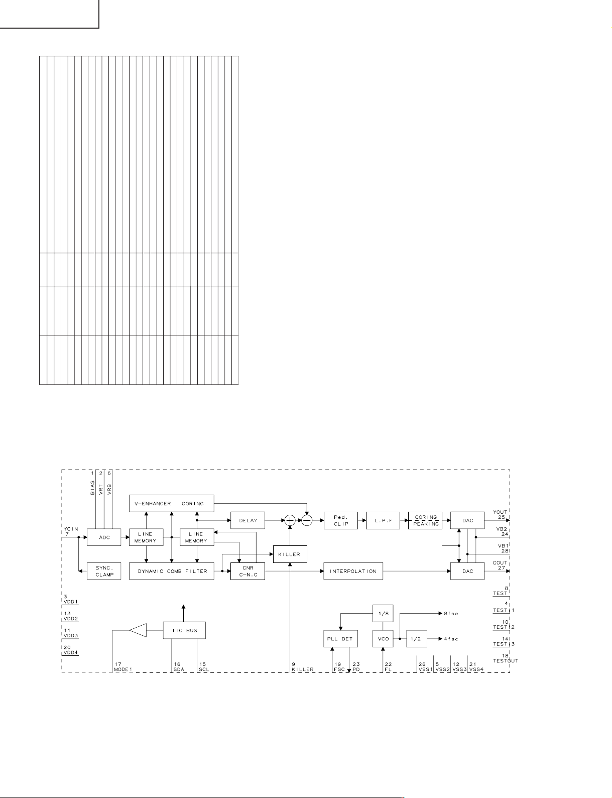
LC-37HV6U
Ë
VHITC90A69F-1Y(ASSY:IC401)
3LINE DIGITAL COMB FILTER(NTSC)
»Block Diagram
»Pin Function
Pin No. Pin Name I/O Pin Function
1 BIAS — Bias for ADC
2 VRT — D range upper bias for ADC
3 VDD1 — Power supply for ADC and DAC (analog system)
4 TESTI1 I Test input
5 VSS2 — GND for ADC (analog system)
6 VRB — D range lower bias for ADC
7 YCIN I Picture signal input
8 TEST O Reset control and TEST control at the time of shipment
9 KILLER I Y/C separation and vertical enhancer-off control
10 TESTI2 I Test input
11 VDD3 — Power supply for logic (digital system)
12 VSS3 — GND for Logic and DRAM (digital system)
13 VDD2 — Power supply for DRAM (digital system)
14 TESTI3 I Test input
15 SCL I Clock input of IIC BUS
16 SDA I Data input of IIC BUS
17 MODE1 O MODE1 output
18 TESTOUT I Test input
19 FSC I Clock input
20 VDD4 — Power supply for PLL (analog system)
21 VSS4 — GND for PLL (analog system)
22 FIL I VCO control
23 PD O PLL detection output
24 VB2 — Bias 2 for DAC
25 YOUT O Luminosity signal output
26 VSS1 — GND for DAC (analog system)
27 COUT O Color signal output
28 VB1 — Bias 1 for DAC
58-2
58-1
58
Page 59

LC-37HV6U
Ë
VHITA1318AF1EY (ASSY:IC604)
Synchronous processing for TV component signals, frequency measurement
»Block Diagram
Pin No. Pin Name I/O Pin Function
»Pin Function
1 HD2-IN I Input the horizontal synchronizing signal.
It's polarity corresponds to both positive and negative.
Input from this pin does not be synchronized internally.
2 VD2-IN I Input the vertical synchronizing signal.
It's polarity corresponds to both positive and negative.
Input from this pin does not be synchronized internally.
3 HD1-IN I Input the horizontal synchronizing signal.
It's polarity corresponds to both positive and negative.
Input from this pin does not be synchronized internally.
4 VD1-IN I Input the vertical synchronizing signal.
It's polarity corresponds to both positive and negative.
Input from this pin does not be synchronized internally.
5 ANALOG GND — The GND pin for analog circuit block.
6 N.C — It is a blank terminal. Please connect with GND.
7 AFC FILTER — Connect the filter for horizontal AFC. The frequency of the horizontal output is
varied by the volyage at this pin.
8 N.C — It is a blank terminal. Please connect with GND.
9 HVCO — Connect the ceramic oscillator for horizontal oscillator.
10 N.C — It is a blank terminal. Please connect with GND.
11 VCC — The VCC pin.(9.0V)
12 DAC2(H/C. O DAC2 output pin. When TEST mode, HD or composite sync signal to frequency
SYNC output) counter circuit is output.
13 VD3-IN I Input the vertical synchronizing signal.
It's polarity corresponds to both positive and negative.
14 HD3-IN I Input the horizontal synchronizing signal.
It's polarity corresponds to both positive and negative.
15 CP-OUT O Clamp pulse output pin. CP according to the incoming signal by which
synchronous reproduction is carried out is outputted.
16 HD1-OUT O HD output pin. This pin is open-collector system.
HD1/HD2 input signal is outputted from this terminal, without carrying out
synchronous processing.
It's polarity is switched by BUS write function.
17 N.C — It is a blank terminal. Please connect with GND.
18 DIGITAL GND — The GND pin for digital circuit block.
19 HD2-OUT O HD output pin. This pin is open-collector system.
HD1/HD2 input signal is outputted from this terminal, without carrying out
synchronous processing.
It's polarity is switched by BUS write function.
20 N.C — It is a blank terminal. Please connect with GND.
21 SDA I/O The SDA pin for I2C BUS.
22 SCL I The SCL pin for I2C BUS.
23 ADDRESS SW I Slave address switch.
24 SYNC2-IN I It is the input of a synchronous separation circuit.
Y signal is inputted through a clamp capacitor.
25 DAC1(V. SYNC O DAC1 output pin. When TEST mode, VD or vertical sync signal to frequency
output) counter circuit is output.
26 SYNC1-IN I It is the input of a synchronous separation circuit.
Y signal is inputted through a clamp capacitor.
27 N.C — It is a blank terminal. Please connect with GND.
28 VD1-OUT O VD output pin. This pin is open-collector system.
VD1/VD2 does not be synchronizing and they are output from this pin.
It's polarity is switched by BUS write function.
29 VD2-OUT O VD output pin. This pin is open-collector system.
VD1/VD2 does not be synchronizing and they are output from this pin.
It's polarity is switched by BUS write function.
30 DAC3 O DAC2 output terminal. This pin is open-collector system. The pulse signal for a
shipment test is outputted at the time of TEST mode.
59-2
59
59-1
Page 60

LC-37HV6U
Ë
VHITB1274AF1EQ (ASSY:IC801,IC802)
VIDEO/CHROMA/SYNC. processor
»Block Diagram
»Pin Function
Pin No. Pin Name I/O Pin Function
1 CVBS1/Y1-IN I CVBS1 or a Y1-IN signal is inputted.
2 SYNC-IN I Synchronized signal is inputted.
3 CVBS-OUT O Output terminal of CVBS or a Y+C signal.
4 VS O Counted-down vertical synchronized signal is outputted.
5 COMB Y-IN I Y-signal outputted from comb-filter is inputted.
It opens, when not using it.
6 D-VDD — Power supply of a DDS/BUS/V-CD/H-CD block is supplied.
DC5V (standard)"
7 COMB C-IN I C-signal outputted from comb-filter is inputted.
It opens, when not using it."
8 D-GND — GND terminal of a DDS/BUS/V-CD/H-CD block.
9 HS O Horizontal synchronized signal which required H-AFC is outputted.
10 SCP O Sand Castle Pulse is outputted. A clamp pulse and a horizontal Blanking pulse
are outputted.
11 Yvi-IN O Y-signal for a synchronous input selected by Video-SW is outputted.
12 SYNC-VCC — Power supply of a SYNC/HVCO block is supplied.
DC5V (standard)
13 SCL I SCL terminal of I2CBUS.
14 SDA I/O SDA terminal of I2CBUS.
15 YS3(RGB1-in) I Selecte SW of a main signal and RGB1 input signal.
Only when "RGB1-ENB" is set as "enable" by bus setup, the input of YS3
becomes effective.
16 SYNC-GND — GND terminal of a SYNC/HVCO block.
17 Cr1-IN I Y1-/Cb1/Cr1 signal is inputted.
18 Cb1-IN I
19 Y1-IN I
20 CLP-FIL — Filter for Y clamp is connected.
21 Y-OUT O Y/Cb/Cr signal is outputted.
22 Cb-OUT O
23 Cr-OUT O
24 YS1(YVbC2-IN) I Selecte SW of a main signal and YCrCb2 input signal.
25 B1-IN I RGB1 signal is inputted. This input is selected in YS3 or I2CBUS.
26 G1-IN I
27 R1-IN I
28 Y/C-GND — GND terminal of Y/C/Text/Video-SW / 1HDL block.
29 Cr2-IN I Y2/Cb2/Cr2 signal is inputted. This input is selected in YS1.
It opens, when not using it.
30 Cb2-IN I
31 Y2-IN I
32 Y/C-VCC — Power supply of Y/C/Text/Video-SW / 1HDL block is supplied.
DC5V (standard)
33 B2-IN I RGB2 signal is inputted. This input is selected in YS2.
It opens, when not using it.
34 G2-IN I
35 R2-IN I
36
YS2/YM(RGB2-IN)
I Selecte SW of a main signal and RGB2 input signal.
37 FIL. — Connects with a Y/C-VCC terminal.
38 X'TAL — 16.2MHz X'tal oscillation element is connected.
39 C3-IN I Chrominance signal is inputted. It opens, when not using it.
40 APC-FIL — Filter for a chrominance demodulater is connected.
41 CVBS3/Y3-IN I CVBS3 or Y3 signal is inputted. It opens, when not using it.
42 ADDRESS I Slave address is set up.
43 C2-IN I Chrominance signal is inputted. It opens, when not using it.
44 CVBS2/Y2-IN I CVBS2 or Y2 signal is inputted. It opens, when not using it.
45 COMB SYS O The distinction result of the received color system is outputted from this terminal
and a terminal 46.
46 Fsc-OUT O Subcarrier is outputted.
47 AFC-FIL — Filter for AFC detection is connected.
48 C1-IN I Chrominance signal is inputted. It opens, when not using it.
60-2
60
60-1
Page 61
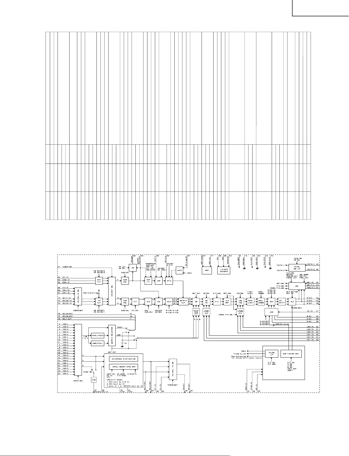
LC-37HV6U
Ë
VHICXA2101Q-1Q(ASSY:IC803)
Multi Component Processor
»Block Diagram
»Pin Function
Pin No. Pin Name I/O Pin Function
1 IN2-H I IN2-H:FIndependent H-synchronization signal input terminal
2 IN2-V I IN2-V:FIndependent V-synchronization signal input terminal
3 IN2-1 I Signal input terminal of IN2 system
4 IN2-2 I
5 IN2-3 I
6 Vcc-MAT
—
Power supply terminal of a selector system and a synchronous processing
system
7 IN3-H I IN3-H:FIndependent H-synchronization signal input terminal
8 IN3-V I IN3-V:FIndependent V-synchronization signal input terminal
9 IN3-1 I Signal input terminal of IN3 system
10 IN3-2 I
11 IN3-3 I
12 GND-MAT
—
Ground terminal of a selector system and a synchronous processing system
13 IN4-H I IN4-H:FIndependent H-synchronization signal input terminal
14 IN4-V I IN4-V:FIndependent V-synchronization signal input terminal
15 IN4-1 I Signal input terminal of IN4 system
16 IN4-2 I
17 IN4-3 I
18 V-PH
—
Capacitor connection terminal for carrying out the peak hold of the V-sync.
19 IN5-H I IN5-HÅFIndependent H-synchronization signal input terminal
20 IN5-V I IN5-VÅFIndependent V-synchronization signal input terminal
21 IN5-1 I Signal input terminal of IN5 system
22 IN5-2 I
23 IN5-3 I
24 H-PH
—
Capacitor connection terminal for carrying out the peak hold of the H-sync.
25 YG-OUT O Composite Video signal output terminal for synchronous separation.
26 YG-IN I Composite Video signal input terminal for synchronous separation.
27 IREF-SYNC
—
Reference current setting terminal (about 4.6 V)
28 VS-OUT O HV of IN1 system or HV of IN2 to IN5 system selector output, and this either are
chosen by I2 C BUS"YCBCR/MAT", and it outputs by positive.
29 HS-OUT O
30 Vcc-OUT O Power supply terminal of RGB system
31 SCP-IN I Input terminal of Sand-Castle-Pulse
32 VTIM-IN I Input terminal of V-timing pulse.
33 HP-IN I Input terminal of H-pulse
34 GND-OUT O Ground terminal of RGB system
35 R-OUT O Output terminal of RGB signal
37 G-OUT O Outputted by 2.6 Vp-p at the time of the input of the white of 100IRE.
39 B-OUT O
36 R-SH
—
Sample & Hold terminal for AKB of RGB
38 G-SH
—
40 B-SH
—
41 IK-IN I Reference pulse is returned to this terminal.
42 PABL-FIL I Peak hold terminal of Peak ABL.
43 ABL-FIL I LPF is formed to an ABL control signal.
44 ABL-IN I ABL control signal input terminal
45 YS/YM-1 I Control input terminal of YM1/YS1
Input level corresponds with three values.
When the value of YM and each YS reaches, it serves also as the function
which turns off VM.
46 LR1-IN I Signal input terminal of analog RGB1
47 LG1-IN I
48 LB1-IN I
49 YS/YM-2 I Control input terminal of YM2/YS2
Input level corresponds with three values.
When the value of YM and each YS reaches, it serves also as the function
which turns off VM.
50 LR2-IN I Signal input terminal of analog RGB2
51 LG2-IN I
52 LB2-IN I
53 ADDRESS I Slave address setting terminal of I2C BUS.
54 DPIC-C
—
Capacitor is connected to black detection of dynamic picture (black extension)
at GND.
55 SCL I Input terminal of SCL(Serial Clock) of a I2C BUS standard.
56 SDA I Input terminal of SDA(Serial Data) of a I2C BUS standard.
57 DPIC-MUTE I MUTE of dynamic picture (black extension) is controllable with a terminal.
58 CLP-C Connection terminal of the capacitor for Y-system clamp.
61-2
61
61-1
Page 62

LC-37HV6U
Pin No. Pin Name I/O Pin Function
59 VM-OUT O VM output terminal. The differentiation waveform of Y-signal is outputted by
positive.
60 VM/SHP/
—
Terminal for turning off VM, SHARPNESS, and COLOUR.
COL-OFF Input level corresponds with three values.
61 YCBCR-SW I Change terminal of a signal inputted into INT/EXT SW.
External input terminal is chosen by High.
62 ECR-IN I Input terminal of Exteriors Y, Cb and Cr.
63 ECB-IN I
64 EY-IN I
65 V1-IN I Input terminal of HV of IN1 system. Positive input.
66 H1-IN I
67 CR1-IN I Input terminal of Y, Cb, and Cr of IN1 system.
68 CB1-IN I
69 Y1-IN I
70 GND-SIG
—
GND terminal of the signal processing system of Y-component
71 IREF-YC
—
Reference current setting terminal (mainly Y-component signal processing
system).
72 Vcc-SIG
—
Power supply terminal of the signal processing system of Y-component.
73 SELCR-IN I Selector outputs Y, Cb, and Cr are inputted through the capacitor for a clamp.
74 SELCB-IN I
75 SELY-IN I
76 SELY-OUT O Selector output terminal of IN2 to IN5.
The signal changed into Y, Cb, and Cr is outputted.
77 SELCB-OUT O
78 SELCR-OUT O
79 SELH-OUT O Selector HV output terminal of IN2 to IN5.
80 SELV-OUT O
ËVHIMM1519XQ-1Q(IC1401)
Component input video switch
»Block Diagram
Pin No. Pin Name I/O Pin Function
»Pin Function
1 VIDEO 1-L1 I Line input of D-terminal
2 VIDEO 1-L2 I
3 VIDEO 1-L3 I
11 VIDEO 2-L1 I
12 VIDEO 2-L2 I
13 VIDEO 2-L3 I
21 VIDEO 3-L1 I
22 VIDEO 3-L2 I
23 VIDEO 3-L3 I
4,14,39,45,52,58 VCC — Analog power supply(9V)
51 AVCC —
5 VIDEO 2-Y I Y-signal input
15 VIDEO 3-Y I
53 TUNER-Y I
59 VIDEO 1-Y I
24 DGND — GND
6,8,16,18,33,35, GND —
37,41,43,47,49,
54,56,60,62
7 VIDEO 2-Pb I Pb,Pr signal input
9 VIDEO 2-Pr I
17 VIDEO 3-Pb I
19 VIDEO 3-Pr I
55 TUNER-Pb I
57 TUNER-Pr I
61 VIDEO 1-Pb I
63 VIDEO 1-Pr I
10 VIDEO 2-SW I Switch line of D-terminal
20 VIDEO 3-SW I
32 MONO-SW I
64 VIDEO 1-SW I
25 ADDRESS I Slave address select pin
26 SDA I/O Data input of I2C bus
27 SCL I Clock input of I2C bus
28 DVCC — Digital power supply(5V)
29 L3 OUT O Line output for monitor
30 L2 OUT O
31 L1 OUT O
34 Pr OUT 3 O Video signal output
36 Pb OUT 3 O
38 Y OUT 3 O
40 Pr OUT 2 O
42 Pb OUT 2 O
44 Y OUT 2 O
46 Pr OUT 1 O
48 Pb OUT 1 O
50 Y OUT 1 O
62-2
62-1
62
Page 63

LC-37HV6U
Ë
VHICXA2069Q-1 (ASSY:IC1301)
S2 correspondence 7 input 3 output AV switch
»Block Diagram
»Pin Function
Pin No. Pin Name I/O Pin Function
63 TV I Video signal input
1 V1 I Composite video signal input
8V2 I
15 V3 I
22 V4 I
30 V5 I
60 V6 I
3 Y1 I Luminance signal is inputted with a Y/C separation signal input terminal.
10 Y2 I YIN1 inputs the signal which carried out Y/C separation of the output of VOUT1.
17 Y3 I
24 Y4 I
49 YIN1 I
5 C1 I Chrominance signal is inputted with the input terminal of Y/C separation signal.
12 C2 I CIN1 inputs the signal which carried out Y/C separation of the output of VOUT1.
19 C3 I
26 C4 I
51 CIN1 I
62,2 LTV,LV1 I Input terminal of an audio signal
9,16 LV2,LV3 I
23,29 LV4,LV5 I
59,64 LV6,RTV I
4,11 RV1,RV2 I
18,25 RV3,RV4 I
31,61 RV5,RV6 I
53 VOUT1 O Composite video signal is outputted with the output terminal of a video signal.
41 VOUT3 O
44 V/YOUT2 O Composite video signal output or a luminance signal output is chosen with the
output terminal of a video signal in I2C Bus control.
56 YOUT1 O Luminance signal is outputted with the output terminal of a video signal.
39 YOUT3 O
58 COUT1 O Chrominance signal is inputted with the output terminal of a video signal.
47 COUT2 O
37 COUT3 O
52 LOUT1 O Audio signal output terminal
43 LOUT2 O
38 LOUT3 O
54 ROUT1 O
45 ROUT2 O
40 ROUT3 O
6 S2-1 I Terminal on which C-signal was overlapped and which detects DC of S2
13 S2-2 I correspondence.
20 S2-3 I Less than 1.3V and they are 4:3 picture signals.
27 S2-4 I More than 1.3V and less than 2.5V, and is a 4:3 letter box signal.
More than 2.5V and is the squeeze signal of 16:9 pictures.
GND at 100KΩ pull-down Since it is carrying out, it becomes 4:3 picture signals
at the time of opening.
7 S-1 I Terminal for a change of composite video/S.
14 S-2 I Detection result is written in a status register.
21 S-3 I Less than 3.5V and is S-signal. More than 3.5V and is a composite video signal.
28 S-4 I Since the pull-up is carried out to 5V by resistance of 100K
É , it becomes a
composite video signal at the open.
32 ADR I I2C Choose the slave address for Bus.
Less than 1.5V and is 90H. More than 2.5V and is 92H. Set to 90H at the time
of terminal opening.
33 SCL I Signal input terminal for I2C Bus.
34 SDA I Signal input terminal for I2C Bus.
36 DC OUT O DC of the S2 correspondence superimposed on COUT3 output is outputted.
DC is superimposed by connecting with COUT3 output through capacity. Control
by I
2
CBus.
When external resistance 4.7Kohm is attached, output impedance 10±3KΩ of
S2 standard is realized.
55 TRAP1 I Trap circuit for subcarriers is connected.
46 TRAP2 I
48 MUTE I Mute terminal for audio signal output
Less than 1.3V and is the mute off.
More than 2.5V and is the mute on.
50 BIAS I Terminal for internal reference bias (Vcc/2).
Connects with GND through a capacitor.
63-2
63
63-1
Page 64

LC-37HV6U
Ë
RH-IXA837WJN1Y (ASSY:IC1601-2)
Single-chip 8-bit CMOS microcomputer with Closed caption decoder and On-screen display controller.
»Block Diagram
»Pin Function
Pin No. Pin Name I/O Pin Function
22,14,21 VCC,AVCC, Power supply — To VCC, AVCC5V ± 10 (Standard) C0V are impressed to VSS.
VSS
18 CNVSS CNVSS Please connect with VSS.
25 RESET Reset input I Required more than 2 mus to reset with a reset input terminal.
19 XIN Clock input I It is the input-and-output terminal of a main clock generating circuit.
20 XOUT Clock output O The clock generating circuit is built in and a setup of oscillation frequency is
performed by connecting a ceramic resonance element or a crystal
oscillation element between XIN and XOUT. When you use an external
clock input, please connect the source of a clock oscillation to a XIN
terminal, and open a XOUT terminal wide.
3,4,5,6,7,8, P00/PWM0~ In/output port I/O A port P0 is an input-and-output port of 8 bits. It has the input-and-output
9,10 P05/PWM5, P0 direction register, and can program whether it is made an input terminal for
P06/INT2/AD4,
every bit, or it is made an output terminal. At the time of reset, it becomes
P07/INT1 input mode. Output form is N channel open DOREIN output.
PWM output O P00 - P05 terminal are the PWM output terminal PWM0 - PWM5, and
common use, respectively. Output form is N channel open DOREIN output.
External I P06 and P07 terminal are the INT external interruption input terminals INT2
interruption and INT1 and common use, respectively.
input
Analog input I P06 terminals are the analog input terminal AD4 and common use.
Pin No. Pin Name I/O Pin Function
35,34,33,32, P10/OUT2, In/output port I/O The port P1 has the function almost equivalent to a port P0 in the input-and-
31,30,29,28 P11/SCL1, P1 output port of 8 bits. Output form is a CMOS output.
P12/SCL2, OSD output O P10 terminals are the OSD output terminal OUT2 and common use. Output
P13/SDA1, form is a CMOS output.
P14/SDA2, Multi-master I/O P11 - P14 terminal are SCL1, SCL2, SDA1, SDA2 and common use,
P15/AD1/INT3,
12 C-BUS respectively at the time of multi-master I2 C-BUS interface use. Output form
P16/AD2, interface is N channel open DOREIN output.
P17/AD3 Analog input I P10, P15 - P17 terminal are the analog input terminals AD8 and AD1 - AD3
and common use, respectively.
External I P15 terminals are the INT external interruption input terminal INT3 and
interruption common use.
input
38,37,36,11, P20/SCLK, In/output port I/O The port P2 has the function almost equivalent to a port P0 in the input-and-
12,13,24,23 P21/SOUT, P2 output port of 8 bits. Output form is a CMOS output
P22/SIN, Serial I/O I/O P20 terminals are the serial I/O synchronous clock input-and-output
P23/TIM3, synchronous terminal SCLK and common use. Output form is N channel open drain
P24/TIM2, clock output.
P25, in/output
P26/OSC1/
Serial I/O data
O P21 terminals are the serial I/O data output terminal SOUT and common
XCIN, output use. Output form is N channel open drain output at the time of serial I/O use.
P27/OSC2/
Serial I/O data
I P22 terminals are the serial I/O data input terminal SIN and common use.
XCOUT input
External clock I P23 and P24 terminal are the external clock input terminals TIM3 and TIM2
input for timer for timers, and common use, respectively.
Clock input I P26 terminals are the clock input terminal OSC1 for OSD, and common
for OSD use.
Clock output O P27 terminals are the clock input terminal OSC2 for OSD, and common use.
for OSD Output form is a CMOS output.
Sub clock I P26 terminals are the sub clock input terminal XCIN and common use.
input
Sub clock O P27 terminals are the sub clock input terminal XCOUT and common use.
output Output form is a CMOS output.
27,26 P30/AD5, In/output port I/O A port P30 and P31 are the input-and-output ports of 2 bits. It has the
P31/AD6, P3 function almost equivalent to a port P0. Output form can choose either a
CMOS output or N channel open drain output.
Analog input I P30 and P31 terminal are the analog input terminal AD5, AD6, and common
use, respectively.
1,2 P50/HSYNC, Input port P5 I Port P5 is the input port of 2 bits.
P51/VSYNC Horizontal I P50 terminals are the horizontal synchronized signal input terminal HSYNC
synchronized for OSD, and common use.
signal
Vertical I P51 terminal is the vertical synchronized signal input terminal VSYNC for
synchronized OSD.
signal
42,41,40,39 P52/R, Output port O P52 - P55 terminal are the output ports of 4 bits. Output form is a CMOS
P53/G, P5 output.
P54/B, OSD output O P52 - P55 terminal are the OSD output terminals R, G, B, and OUT1 and
P55/OUT1 common use, respectively. Output form is a CMOS output.
17 CVIN Data slicer I Please input a composite video signal through a capacitor.
in/output
16 VHOLD I Please connect a capacitor between VHOLD and VSS.
15 HLF I/O Please connect the filter which consists of a capacitor and resistance
between HLF and VSS.
64-2
64
64-1
Page 65

LC-37HV6U
Ë
VHISII907++-1Q(ASSY: IC1650)
HDCP_LSI
»Block Diagram
Pin No. Pin Name I/O Pin Function
42 ODCK O Output Data Clock.
44 DE O Output Data Enable. This signal qualifies the active data area.
18 HSYNC O Horizontal Sync control signal.
19 VSYNC O Vertical Sync control signal.
23 IOR O RED Analog Out.
26 IOG O GREEN Analog Out.
31 IOB O BLUE Analog Out.
30 COMP I Compensation. Provides compensation for the internal reference amplifier.
This pin should be connected through a 0.01_F ceramic capacitor and a 10_F
tantalum capacitor to DACVCC externally. These capacitors must be as close to
the pin as possible to avoid any noise pick-up.
29 RSET I Full Scale Adjust Resistor. A precision resistor (1%) connected between this pin
and DACGND controls the magnitude of the full scale video signal. RSET may
need to be adjusted for optimum gain; see page 16 for recommended values.
This resistor must be as close to the pin as possible to avoid any noise pick-up.
40 SCDT O Sync Detect. A HIGH level is output when DE is actively toggling, indicating that
the link is alive. When DE is inactive, a LOW level is output indicating the link is
down. SCDT is internally connected to PD_DAC# and has the same effect as
PD_DAC# driven low externally (see below). SCDT can be left unconnected,
tied to PD_DAC# (redundant to internal connection), or used by an external
circuit to monitor the link activity. The SCDT output remains in the active mode
at all times.
20 PD_DAC# I DAC Power Down (active LOW). A HIGH level puts the DAC in normal
operation. A LOW level powers down the DAC and puts all the video data
outputs into a high impedance (tri-state) mode with a weak internal pull-down
device bringing the outputs to ground. The HSYNC, VSYNC, and DE signals are
not affected. Only the DAC is powered down in this mode; the chip itself is not in
full power-down mode with this pin. Tie high through pullup resistor if not used.
»Pin Function
Pin No. Pin Name I/O Pin Function
11 PD# I Power Down (active LOW). A HIGH level puts the chip in normal operation.
A LOW level puts the chip in full power down mode. During this mode the
following occur: the receiver core, DAC and all analog logic are powered down;
all outputs (including HSYNC, VSYNC, DE, ODCK, and data signals) are
brought to logic zero (0) state. Tie high through pullup resistor if not used.
2 RX0+ Analog Receiver Data. TMDS low voltage differential signal input data pairs.
3 RX0_ Analog
51 RX1+ Analog
52 RX1_ Analog
48 RX2+ Analog
49 RX2_ Analog
5 RXC+ Analog Receiver Clock. TMDS low voltage differential signal input clock pair.
6 RXC_ Analog
8 EXT_RES Analog Impedance Matching Control. In the common case of 50_ transmission line, an
external 412_ 1% resistor is recommended for connection between AVCC and
this pin.
15 SCLS I I2C Clock. This is a slave I2C clock interface for communicating with a host side
master. The clock may be run up to 400kHz. This pin is not 5V tolerant and
should go through a level shifter for connection to the DDC clock line.
14 SDAS I/O I2C Data. This is a slave I2C data interface for communicating with a host side
master. Data may be clocked in at up to 400kHz. This pin is not 5V tolerant and
should go through a level shifter for connection to the DDC data line.
39 RESET# I Power-On Reset. This pin acts as active LOW reset for the cipher block logic.
It must be held low for at least 100ns after power up. For HDCP applications,
this pin should be connected to an external power-on reset circuit that causes
this signal to go high after the required low period. For non-HDCP applications,
this pin should always be tied LOW.
13,22,46 VCC Power Digital Core VCC, must be set to 3.3V.
12,21,45 GND Ground Digital Core GND.
17,41 OVCC Power Digital Output VCC, must be set to 3.3V.
16,43 OGND Ground Digital Output GND.
1,7 AVCC Power TMDS Analog VCC must be set to 3.3V.
4,47,50 AGND Ground TMDS Analog GND.
9 PVCC Power PLL Analog VCC must be set to 3.3V.
10 PGND Ground PLL Analog GND.
37 DACVCC Power DAC Analog VCC, must be set to 3.3V.
35 DACGND Ground DAC Analog GND.
24 DACVCCR Power DAC Red VCC, must be set to 3.3V.
25 DACGNDR Ground DAC Red GND.
27 DACVCCG Power DAC Green VCC, must be set to 3.3V.
28 DACGNDG Ground DAC Green GND.
32 DACVCCB Power DAC Blue VCC, must be set to 3.3V.
33 DACGNDB Ground DAC Blue GND.
34 No Connect No Connect These pins should normally be unconnected, but can be left connected to pull-
ups if desired.
36 No Connect No Connect
38 Reserved Reserved This pin must be tied HIGH for normal operation.
65-2
65
65-1
Page 66

LC-37HV6U
Ë
VHIFA3675F/-1 (ASSY:IC1702)
6-channel DC-DC converter IC
»Block Diagram
»Pin Function
Pin No. Pin Name I/O Pin Function
1 VCC1 — Power supply for control circuit.
2RT — Oscillator timing resistor.
3CT — Oscillator timing capacitor.
4 CS3 — Soft start for Ch.3 & Ch.4.
5 CS5 — Soft start for Ch.6.
6 CS4 — Soft start for Ch.5.
7 CS1 — Soft start for Ch.1
8 CS2 — Soft start for Ch.2.
9 VREF O Reference voltage output.
10 CREF O Capacitor for reference voltage output.
11 VREG O Regulated for voltage output.
12 IN2- I Ch.2 inverting input to error amplifier.
13 FB2 O Ch.2 output of error amplifier.
14 IN1- I Ch.1 inverting input to error amplifier.
15 FB1 O Ch.1 output of error amplifier.
16 IN5+ I Ch.5 non-inverting input to error amplifier.
17 IN5- I Ch.5 inverting input to error amplifier.
18 FB5 O Ch.5 output of error amplifier.
19 IN6- I Ch.6 inverting input to error amplifier.
20 FB6 O Ch.6 output of error amplifier.
21 IN3+ I Ch.3 non-inverting input to error amplifier.
22 IN3- I Ch.3 inverting input to error amplifier.
23 FB3 O Ch.3 output of error amplifier.
24 IN4+ I Ch.4 non-inverting input to error amplifier.
25 IN4- I Ch.4 inverting input to error amplifier.
26 FB4 O Ch.4 output of error amplifier.
27 CP I Timing capacitor for timer latch delay.
28 GND — Ground.
29 TLSEL I Ch.3 & Ch.4 timer latch selection(Low:disable).
30 CNT5 I Ch.6 ON/OFF function.
31 CNT4 I Ch.5 ON/OFF function.
32 CNT2 I Ch.2 ON/OFF function.
33 CNT3 I Ch.3 & Ch.4 ON/OFF function.
34 CNT1 I Ch.1 ON/OFF function.
35 VCC2 — Power supply for output stage.
36 VDRV O Bias for logic circuit of output.
37 PGND1 — Power ground.
38 OUT1S O Ch.1 source electrode of output stage.
39 OUT1 O Ch.1 output(for Pch-MOSFET)
40 OUT4 O Ch.4 output(for Pch-MOSFET)
41 OUT3 O Ch.3 output(for Pch-MOSFET)
42 OUT2S O Ch.2 source electrode of output stage.
43 OUT2 O Ch.2 output(for Pch-MOSFET)
44 OUT6S O Ch.6 source electrode of output stage.
45 OUT6 O Ch.6 output(for Pch-MOSFET)
46 OUT5 O Ch.5 output(for Pch-MOSFET)
47 OUT5S O Ch.5 source electrode of output stage.
48 PGND2 — Power ground.
66-2
66
66-1
Page 67

LC-37HV6U
Ë
VHIMD1422N+-1Y(ASSY:IC1706)
DC-DC converter power IC
»Block Diagram
Pin No. Pin Name I/O Pin Function
1 S/S I capacitor connection terminal for a soft start.
2 OCL- I Over(–) current-detection terminal.
3 OCL+ I Over-current (+) detection terminal.
4,26 GND — GND terminal.
5 R/C I Remote ON/OFF control terminal.
6 Vcc — Power supply terminal of a control circuit.
8 Vboot I Power supply terminal of a main switch and MOSFET control circuit.
9 VGL I Gate terminal of the Low side MOSFET for periodic rectification.
11~14 VOUT O Output terminal of the power stage.
16 P.GND — GND terminal of an output circuit.
18~21 VDD — Power supply terminal of the main switch MOSFET.
23 VGH I Gate terminal of the high side MOSFET for periodic rectification.
25 VB I Output bootstrap terminal.
Capacitor is connected between VB terminal and VOUT and the circuit for
control of MOSFET inside IC is bootstrapped.
27 VTS — Terminal for TEST. Please do not connect anywhere.
28 Vref I Internal standard voltage output terminal.
30 ampOUT O Built-in error amplifier output terminal.
32 amp- I Built-in error amplifier reversal input terminal. .
7,10,15,17, N/C — It is a no-connection terminal.
22,24,29,31
»Pin Function
Ë
RH-IXA802WJN3Q(ASSY:IC1901)
PLD(Programmable Logic Device)
»Pin Function
Pin No. Pin Name I/O Pin Function
1NC — Non connection
2 SP_CP2 I Clamp signal input terminal from the synchronous separation IC.
(with 15k system)
3 SP_VD I Vertical synchronized signal input terminal from the synchronous separation IC
4 GND — Ground
5 SP_HD I Horizontal synchronized signal input terminal from the synchronous separation
IC
6 VD3 O Vertical synchronized signal output terminal to the synchronous separation IC
7 HD3 O Horizontal synchronized signal output terminal to the synchronous separation IC
8 SP_CP1 I Clamp signal input terminal from the synchronous separation IC.
(with normally)
9 TDI I Data input terminal for ISP
10 TMS I Mode input terminal for ISP
11 TCK I Clock input terminal for ISP
12 TEXT_HD O TEXT_HD output terminal
13 US_HD I RCA/TEXT horizontal synchronized input terminal
14 TEXT_VD O TEXT_VD output terminal
15 Vcc3.3V — Power supply terminal
16 US_VD I RCA/TEXT vertical synchronized input terminal
17 GND — Ground
18 MODEA I Mode selection signal A
19 MODEB I Mode selection signal B
20 MODEC I Mode selection signal C
21 SELA I MAIN, VIDEO, CHROME/ RCA HD change control signal
22 SELO I Synchronized signal output control signal input terminal for TEXT
23 SELC I HD change control signal input terminal for closed captions
24 TDO O Data output for ISP
25 GND — Ground
26 Vcc3.3V — Power supply terminal
27 VD1 I MAIN, VIDEO, CHROME vertical synchronized signal input terminal from IC
28 HD1 I MAIN, VIDEO, CHROME horizontal synchronized signal input terminal from IC
29 PL_VD O Vertical synchronized output terminal
30 PL_HD O Horizontal synchronized output terminal
31 PL_CP O Clamp signal output terminal
32 PL_BLK O H blank signal output terminal
33 MODED I Mode selection signal D
34 NC — Non connection
35 Vcc3.3V — Power supply terminal
36 NC — Non connection
37 CC_HD O Horizontal synchronized signal for closed caption
38 ow_vblk I V blank signal input terminal for auto wide
39 HDS O Horizontal synchronized signal output terminal for PC board.
40 VDS O Vertical synchronized signal output terminal for PC board.
41 HD2 I Horizontal synchronized signal input terminal from SUB, VIDEO, CHROME IC
42 VD2 I Vertical synchronized signal input terminal from SUB, VIDEO, CHROME IC
43 CLK I Clock input
44 NC — Non connection
67-2
67
67-1
Page 68

LC-37HV6U
Ë
RH-IX3370CEN1Q(ASSY:IC2501)
Multi Standard Sound Processor
»Block Diagram
»Pin Function
Pin No. Pin Name I/O Pin Function
1NC — Not connected
2 I2C_CL I/O I2C clock
3 I2C_DA I/O I2C data
4 I2S_CL I/O I2S clock
5 I2S_WS I/O I2S word strobe
6 I2S_DA_OUT O I2S data output
7 I2S_DA_IN1 I I2S1 data input
8 ADR_DA O ADR data output
9 ADR_WS O ADR word strobe
10 ADR_CL O ADR clock
11,12,13 DVSUP — Digital power supply 5V
14,15,16 DVSS — Digital ground
17 I2S_DA_IN2 I I2S2-data input
18 NC — Not connected
19 I2S_CL3 I I2S3 clock
20 I2S_WS3 I I2S3 word strobs
21 RESETQ I Power-on-reset
22 I2S_DA_IN3 I I2S3-data input
23 NC — Not connected
24 DACA_R O Headphone out, right
25 DACA_L O Headphone out, left
26 VREF2 — Reference ground 2
27 DACM_R O Loudspeaker out, right
28 DACM_L O Loudspeaker out, left
29,30,31,32 NC — Not connected
33 SC2_OUT_R O SCART 2 output, right
34 SC2_OUT_L O SCART 2 output, left
35 VREF1 — Reference ground 1
36 SC1_OUT_R O SCART 1 output, right
37 SC1_OUT_L O SCART 1 output, left
38 CAPL_A — Volume capacitor AUX
39 AHVSUP — Analog power supply 8V
40 CAPL_M — Volume capacitor MAIN
41,42 NC — Not connected
43,44 AHVSS — Analog ground
45 AGNDC — Analog reference voltage
46 NC — Not connected
47 SC4_IN_L I SCART 4 input, left
48 SC4_IN_R I SCART 4 input, right
49 ASG — Analog Shield Ground
50 SC3_IN_L I SCART 3 input, left
51 SC3_IN_R I SCART 3 input, right
52 ASG — Analog Shield Ground
53 SC2_IN_L I SCART 2 input, left
54 SC2_IN_R I SCART 2 input, right
55 ASG — Analog Shield Ground
56 SC1_IN_L I SCART 1 input, left
57 SC1_IN_R I SCART 1 input, right
58 VREFTOP — Reference voltage IF A/D converter
59 NC — Not connected
60 MONO_IN I Mono input
61,62 AVSS — Analog ground
63,64 NC — Not connected
65,66 AVSUP — Analog power supply 5V
67 ANA_IN1+ I IF input 1
68 ANA_IN- I IF common(can be left vacant, only if IF input 1 is also not in use)
69 ANA_IN2+ I IF input 2(can be left vacant, only if IF input 1 is also not in use)
70 TESTEN I Test pin
71 XTAL_IN I Crystal oscillator
72 XTAL_OUT O
73 TP — Test pin
74 AUD_CL_OUT O Audio clock output(18.432MHz)
75,76 NC — Not connected
77 D_CTR_I/O_1 I/O D_CTR_I/O_1
78 D_CTR_I/O_0 I/O D_CTR_I/O_0
79 ADR_SEL I I2C Bus address select
80 STANDBYQ I Stand-by(low-active)
68-2
68
68-1
Page 69

LC-37HV6U
Ë
VHINJU26150-1Q(ASSY:IC2518)
DIGITAL AUDIO PROCESSOR
»Block Diagram
Pin No. Pin Name I/O Pin Function
»Pin Function
1 SDO2 O Sound data output CH2
2 SDO1 O Sound data output CH1
3 SDO0 O Sound data output CH0
4 SDA2 I/O I2C I/O (for download)
5 SCL/SCK I I2C clock / serial clock
6 SDA/SDOUT I/O I2C I/O / serial out
7 AD1/SDIN I I2C address / serial in
8 AD2/SSX I I2C address / serial enable
9 VDDO — Power supply for oscillator (+2.5V)
10 XI I Clock input terminal
11 XO O Output for VCO connection
12 VSSO — Oscillator power supply GND
13 RESET I Reset terminal
14 VDDC — Internal power supply +2.5V
15 VSSC — Internal power supply GND
16 SCL2 I/O I2C clock output (for download)
17 VDDC — Internal power supply +2.5V
18 VDDC — Internal power supply +2.5V
19 VSSC — Internal power supply GND
20 VSSC — Internal power supply GND
21 VDDR — Power supply for I/O (+2.5V)
22 VDDR — Power supply for I/O (+2.5V)
23 VSSR — I/O ground
24 VSSR — I/O ground
25 SDI0 I Sound data output channel 0
26 SDI1 I Sound data output channel 1
27 SDI2 I Sound data output channel 2
28 LRI I LR clock input
29 BCKI I Bit clock input
30 MCK O A/D, D/A clock input
31 BCKO O Bit clock output
32 LRO O LR clock output
Ë
VHINJU26106-1Q(ASSY:IC2521)
DOLBY PROLOGIC II/VIRTUAL DOLBY SURROUND
»Block Diagram
Pin No. Pin Name I/O Pin Function
»Pin Function
1 TEST0 O Sound data output CH2
2 TEST1 O Sound data output CH1
3 SDO0 O Sound data output CH0
4 SEL1 I I2C(="L"),serial(="H") setup
5 SCL/SCK I I2C clock / serial clock
6 SDA/SDOUT I/O I2C I/O / serial out
7 AD1/SDIN I I2C address / serial in
8 AD2/SSX I I2C address / serial enable
9 VDDO — Power supply for oscillator (+2.5V)
10 XI I Clock input terminal
11 XO O Output for VCO connection
12 VSSO — Oscillator power supply GND
13 RESETX I Reset
14 VDDC — Internal power supply +2.5V
15 VSSC — Internal power supply GND
16 TEST2 I/O When using it, it connects with open.
17 VDDC — Internal power supply +2.5V
18 VDDC — Internal power supply +2.5V
19 VSSC — Internal power supply GND
20 VSSC — Internal power supply GND
21 VDDR — Power supply for I/O (+2.5V)
22 VDDR — Power supply for I/O (+2.5V)
23 VSSR — I/O ground
24 VSSR — I/O ground
25 SDI0 I Sound data input 0
26 SDI1 I Sound data input 1
27 TEST3 I When using it, it connects with GND.
28 LRI I LR clock input
29 BCKI I Bit clock input
30 MCK O A/D, D/A clock output
31 BCKO O Bit clock output
32 LRO O LR clock output
69-2
69
69-1
Page 70

LC-37HV6U
Ë
VHIPD64084+-1Q(ASSY:IC7001)
3-dimensional Y/C separation LSI with a built-in 4 M bit memory
»Block Diagram
»Pin Function
Pin No. Pin Name I/O Pin Function
1,33,48,75 DGND — Digital part GND (common to I/O part grounding)
39,62,100 DVDD — Digital part 2.5V power supply
4-12,28-30,32, TEST01-TEST26 Test terminal (OPEN or GND connection)
40-43,78-85,99
13 EXTALTF O Extended 4fsc and an alternat-flag output terminal
14-23 EXTDYCO0- I/O Extended digital input-and-output terminal
EXTDYCO9
24-25 DGNDRAM — DRAM part GND
26-27 DVDDRAM — DRAM part 2.5V power supply
31 DVDDIO — I/O part 3.3V power supply
34-35 AGND — OSC circuit part GND
36 XI I Standard clock input
37 XO O Standard clock reversal output
38 AVDD — OSC circuit part 2.5V power supply
44 RPLL I Test input terminal (GND connection)
45 SLA0 I I2C-bus slave address selection input
46 SCL I I2C-bus clock input
47 SDA I/O I2C-bus clock output
49 AGND — I2C-bus data input-and-output terminal
50 AVDD — fsc DAC section 2.5V power supply
51 FSCO O fsc generator fsc output
52-53 AGND — 8fsc PLL section grounding
54 FSCI I 8fsc PLL fsc input
55 AVDD — 8fsc PLL section 2.5V power supply
56 CKMD I CLK8 test mode selection (GND connection)
57 CLK8 I/O CKMD = 0 : 8fsc clock output
CKMD = 1 : 8fsc clock input
58 RSTB I System reset input (active low)
59 ST0 O Internal signal monitor output
60 ST1 O Internal signal monitor output
61 NSTD O Non-standard detection monitor output
(L : A standard judging , H : Non-standard judging)
63-72 DYCO0-DYCO9 I/O Digital input and output
73 ALTF O 4fsc alternat-flag output
74 LINE I Compulsive line processing selection input
(L : It is usually Processing H. : Processing between compulsive lines)
76 KIL I External killer input
(L : It is usually Processing H. : Compulsive Y/C separation stop)
77 CSI I Composite sync. input (active low)
2 TESTIC1 I The test terminal for IC sorting (GND connection)
3 TESTIC2 I The test terminal for IC sorting (GND connection)
86 AVDD — Y-DAC and C-DAC part 2.5V power supply
87 CBPC O C-DAC phase compensation output
88 ACO O C-DAC analog C-signal output
89 AYO O C-DAC analog Y-signal output
90 CBPY O Y-DAC phase compensation output
91 AGND — Y-DAC and C-DAC part grounding
92 AGND — ADC section grounding
93 AYI I ADC analog composite signal input
94 VCLY O ADC clamp potential output
95 VRBY O ADC bottom standard voltage output
96 VRTY O ADC top standard voltage output
97 VCOMY O ADC standard voltage of the same phase
98 AVDD — ADC section 2.5V power supply
70-2
70
70-1
Page 71

LC-37HV6U
Ë
RH-IX3289CEZZ(ASSY:IC7200)
Auto Wide IC
»Pin Function
Pin No. Pin Name I/O Pin Function
1 GND — Ground
2 VCC — Power supply(3.3V)
3 CKIN I
4 CKOUT O
5 VCC — Power supply(3.3V)
6 GND — Ground
7 TEST I N.C
8 ASD0 O AWDATA
9 TPI I AWCS_W
10 TCI I D_CLK
11 TDI I D_DATAOUT
12 SIREI I AWCS_R
13 VCC — Power supply(3.3V)
14 HER1 O N.C
15 HER2 O N.C
16 VMSET I N.C
17 VCKIN I Ground
18 VCKO O N.C
19 VDIN I VDIN
20 HD I HD
21 HOVBLK O N.C
22 GND — Ground
23 TESTOUT O N.C
24 GND — Ground
25 OUT0 O N.C
26 OUT1 O N.C
27 VCC — Power supply(3.3V)
28 OUT2 O N.C
29 OUT3 O N.C
30 OUT4 O N.C
31 VTS I N.C
32 HTS I N.C
33 OUTSWI I N.C
34 ASDOCNTOUT O ASDOCNTOUT
35 DIA I N.C
36 MTESTI I N.C
37 ANSWIO I ANSWIO
38 ANSWOI O ANSWOI
39 GND — Ground
40 PRS I PRS
41 IPIN I N.C
42 VCC — Power supply(3.3V)
43 HIN I AT_HD
44 VIN I AT_VD
Ë
RH-IX3270CEZZ (ASSY:IC10001)
32bit RISC Micro Processor
»
Block Diagram
71-2
71-1
71
Page 72
LC-37HV6U
Pin No. Pin Name I/O Pin Function
»Pin Function
34,36-44, D[15:0] I/O Data bus D[15:0]
46,48-52
23-26,28,30-32 D[23:16/PTA[7:0] I/O Data bus D[23:16]/I/O port A[7:0]
13-18,20,22 D[31:24/PTB[7:0] I/O Data bus D[31:24]/I/O port B[7:0]
86,84,82,78-72, A[25:0] O Address bus A[15:0]
70-68-60,56-53
96 CS0 O Chip select 0
98 CS2/PTK[0] O/(I/O) Chip select 2/I/O port K[0]
99 CS3/PTK[1] O/(I/O) Chip select 3/I/O port K[1]
100 CS4/PTK[2] O/(I/O) Chip select 4/I/O port K[2]
101 CS5/CE1E/PTK[3] O/(I/O) Chip select 5/CE1(area 5SPCMIA)/O port K[3]
102 CS6/CE1B 0 Chip select 6/CE1(area 6SPCMIA)
87 BS/PTK[4] O/(I/O) Bus cycle startup signal /I/O port K[4]
118 RAS3U/PTE[2] O/(I/O) "RAS(area 3DRAM,SDRAM upper 32MB address)/I/O port E[2}"
106 RAS3L/PTJ[0] O/(I/O) "RAS(area 3DRAM,SDRAM upper 32MB address)/I/O port J[0}"
119 RAS2U/PTE[1] O/(I/O) "RAS(area 2DRAM,SDRAM upper 32MB address)/I/O port E[1}"
107 RAS2L/PTJ[1] O/(I/O) "RAS(area 2DRAM,SDRAM upper 32MB address)/I/O portJE[1}"
108
CASLL/CAS/PTJ[2]
O/(I/O) CAS(DRAM)/CAS(SDRAM)/I/O port J[2] for D7-D0.
110 CASLH/PTJ[3] O/(I/O) CAS(DRAM)/I/O port J[3] for D15-D18.
112 CASHL/PTJ[4] O/(I/O) CAS(DRAM)/I/O port J[4] for D23-D16.
113 CASHH/PTJ[5] O/(I/O) CAS(DRAM)/I/O port J[5] for D31-D24.
116 CAS2L/PTE[6] O/(I/O) CAS(area 2DRAM)/I/O port E[6] for D7-D0.
117 CAS2H/PTE[3] O/(I/O) CAS(area 2DRAM)/I/O port E[3] for D15-D8.
89 WE0/DQMLL O D7-D0 selection signal/DQM(SDRAM)
90 WE1/DQMLU/WE O D15-D8 selection signal/DQM(SDRAM)/PCMCIA WE
91 WE2/DQMUL/ O/(I/O) D23-D16 selection signal/DQM(SDRAM)/PCMCIA I/O port K[6]
ICIORD/PTK[6]
92 WE3/DQMUU/ O/(I/O) D31-D24 selection signal/DQM(SDRAM)/PCMCIA I/O write/I/O port K[7]
ICIOWR/PTK[7]
93 RD/WR O Read/write change signal
88 RD O Read strobe
105 CKE/PTK[5] O/(I/O) CK enable(Only for SDRAM)/I/O port K[5]
123 WAIT I Hardware weight demand.
11-8 IRL[3:0]/IRQ[3:0]/ I External interruption demand/I/OportH[3:0]
PTH[3:0]
12 IRQ4/PTH[4] I External interruption demand/I/OportH[4]
7 NMI I Non maskable interruption demand.
160 IRQOUT O Interruption demand output
182 WAKEUP/PTD[3] O/(I/O) Interruption demand output at the time of standby mode/I/OportD[3]
159 TCLK/PTH[7] I/O Clock input output/I/OportH[7] for TMU/RTC.
191 DREQ0/PTD[4] I DMA demand 0/I/OportD[4]
114 DACK0/PTD[5] O/(I/O) DMA acknowledge 0/I/O port D[5]
192 DREQ1/PTD[6] I DMA demand 0/I/O port D[6]
115 DACK1/PTD[7] O/(I/O) DMA acknowledge 1/I/O port D[7]
189 DRAK0/PTD[1] O/(I/O) DMA acknowledge 0/I/O port D[1]
190 DRAK1/PTD[0] O/(I/O) DMA acknowledge 0/I/O port D[0]
171 RxD0/SCPT[0] I Input port [0] for receiving data 0/SCI.
164 TxD0/SCPT[0] O Output port [0] for transmission data 0/SCI.
165 SCK0/SCPT[1] I/O I/O port [1] for serial clock 0/SCI.
172 RxD1/SCPT[2] I Input port [2] for receiving data 1/SCI.
166 TxD1/SCPT[2] O Output port [2] for transmission data 1/SCI.
167 SCK1/SCPT[1] I/O I/O port [3] for serial clock 1/SCI.
174 RxD2/SCPT[4] I Input port [4] for receiving data 2/SCI.
168 TxD2/SCPT[4] O Output port [4] for transmission data 2/SCI.
169 SCK2/SCPT[5] I/O I/O port [5] for serial clock 2/SCI.
170 RTS2/SCPT[6] O/(I/O) Requests to Send 2/for SCI/I/O port [6]
176
CTS2/IRQ5/SCPT[7]
I Transmitting clearance 2/an external interruption demand/Input port [7] for SCI.
104 CE2B/PTE[5] O/(I/O) Chip enable 2/I/O port E[5] for Pc card 0.
126 IOIS16/PTG[7] I Write protection/Input port G[7]
103 CE2A/PTE[[4] O/(I/O) Chip enable 2/I/O port E[4] for PC card 1.
146,149 CAP[1:2] — External capacity terminal for PLL [1:2]
156 EXTAL I External clock/Crystal oscillation element terminal
155 XTAL O Crystal oscillation element terminal
162 CKIO I/O System clock input and output
5 EXTAL2 I Crystal oscillation element terminal for RTC.
4 XTAL O Crystal oscillation element terminal for RTC.
193 RESETP I Power-on reset demand
124 RESETM I Manual reset demand
Pin No. Pin Name I/O Pin Function
122 BREQ I Bus demand
121 BACK O Bus acknowledge.
2,1,144 MD[2:0] I Clock mode setup
196,195 MD[4:3] I Area 0 bus wide setup.
197 MD5 I Endian setup
194 CA O Chip active.
158,157 STATUS[1:0]/ I/O Processor status[1:0]/I/O port J[7:6]
PTJ[7:6]
204-199 AN[5:0]/PTL[6:7] I A/D conversion input[5:0]/input port L[5:0]
206,207 AN[6:7]/DA[1:0]/ I/O A/D conversion input[6:7]/D/A conversion output[1:0]/input port L[6:7]
PTL[6:7]
177-180,185-188
PTC[7:0]/PINT[7:0]
I/O I/O port C[7:0]/port Interruption [7:0]
184
PTD[2]/RESETOUT
I/O I/O port D[2]/reset output
120,94 PTE[0]/PTE[7] I/O I/O port E[0]/I/O port E[7]
136-143
PTF[7:0]/PINT[15:8]
I I/O port F[7:0]/port Interruption [15:8]
127-131,135 PTG[6:0] I I/O port G[6:0]
125 PTH[5]/ADTRG I I/O port H[5]/Analog trigger
151 PTH[6] I I/O port H[6]
21,29,35,47,59, Vcc — power supply (3.3V)
71,81,85,97,111,
134,154,163,175,
183
145,150 Vcc(PLL) — power supply (3.3V)
3 Vcc(RTC) — power supply (3.3V)
205 Avcc — Analog power supply (3.3V)
19,27,33,45,57, Vss — power supply (0V)
69,79,83,95,109,
132,152,153,161,
173,181
147,148 Vss(PLL) — power supply (0V)
6 Vss(TRC) — power supply (0V)
198,208 Avss — Analog power supply (0V)
72-2
72
72-1
Page 73

LC-37HV6U
Ë
9DK001-15079(CXA3506R) (ASSY:IC10004)
3ch 8bit 120MSPS A/D CONVERTER AMP. PLL
»Block Diagram
»Pin Function
Pin No. Pin Name I/O Pin Function
1 B/CbOUT O Amplifier output signal monitor
2 ADDRESS I I2C slave address setup
3 R/CrOUT O Amplifier output signal monitor
4NC — Not connected
5NC — Not connected
6 XPOWERSAVE I Power save setup
7 DGNDREG — GND for registers
8 DVCCREG — Power supply for registers
9 SDA I Control register data input
10 SCL I Control register clock signal input
11 XSENABLE I Enable signal input for 3 line control registers
12 SEROUT O 3 line control register data read-out
13 3WIRE/I2C I Selection in I2C-bus mode and 3 line bus mode
15 AVCCADREF — Power supply for reference voltage of ADC
16,94 AVCCAD3 — Analog power supply of ADC
17 VRT O The top reference voltage output of ADC
18,92 DVCCAD3 — Digital power supply of ADC
19,32,42,54, DVCCADTTL — Power supply for a TTL output of ADC
65,76,90
20,33,44,55, DGNDADTTL — GND for a TTL output of ADC
67,77,89
21,22,24-28,31 RA0~RA7 O R channel port A side data output
23,30,43,50, DGNDAD3 — Digital GND of ADC
59,66,79,86
29,80 AGNDAD3 — Analog GND of ADC
34-41 RB0~RB7 O R channel port B side data output
Pin No. Pin Name I/O Pin Function
45-49,51-53 BA0~BA7 O B channel port A side data output
56-58,60-64 BB0~BB7 O B channel port B side data output
68-75 GA0~GA7 O G channel port A side data output
78,81-85,87,88 GB0~GB7 O G channel port B side data output
91 DVCCAD — Digital power supply of ADC
93 VRB O Bottom reference voltage output of ADC
95 AGNDADREF — GND for reference voltage of ADC
96 DVCCPLLTTL — Power supply for a TTL output of PLL
97 DGNDPLLTTL — Power supply for a TTL output of PLL
98 XCLKCLK O CLK reversal output
99 1/2XCLK O CLK output
100 1/2CLK O 1/2 CLK reversal output
101 DSYNC/ O 1/2 CLK output
103 DIVOUT O DSYNC signal output /DIVOUT signal output.
104 UNLOCK O UNLOCK signal output terminal.
105 SOGOUT O Sync signal output of a sync-on green signal.
106 HOLD I Input of the de-sable signal of phase comparison.
107 XTLOAD I Reset setup of a programmable counter.
108 EVEN/ODD I Sampling clock reversal pulse input of ADC.
109 XCLKIN I Negative clock input for a test.
110 CLKIN I Positive clock input for a test.
111 SYNCIN1 I Sync signal input1
112 SYNCIN2 I Sync signal input2
113 CLPIN I Clamp pulse input.
114 DVCCPLL — Digital power supply for PLL.
115 DGNDPLL — Digital GND for PLL.
116 AVCCVCO — Analog power supply for VCO of PLL.
117 AGNDVCO — Analog GND for VCO of PLL.
118 RC1 — PLL loop filter external terminal-1.
119 RC2 — PLL loop filter external terminal-2.
120 AVCCIR — Analog power supply for IREF
121 IREF I Current setup
123 AGNDIR — Analog GND for IREF
124 G/YIN1 I G/Y signal input-1
125 AVCCAMPG — Power supply for G/Y amplifier parts
126 G/YIN2 I G/Y signal input-2
127 AGNDAMPG — GND for G/Y amplifier parts
128 G/YCLP — Clamp capacitor connection terminal for brightness
129 B/CbCLP — Clamp capacitor connection terminal for brightness
130 R/CrCLP — Clamp capacitor connection terminal for brightness
132 SOGIN1 I sync-on green signal input-1.
133 B/CbIN1 I B/Cb signal input-1
134 AVCCAMPB — Power supply for B/Cb amplifier parts
135 SOGIN2 I sync-on green signal input-2.
136 B/CbIN2 I B/Cb signal input-2
137 AGNDAMPB — GND for B/Cb amplifier parts
139 R/CrIN1 I R/Cr signal input-1
140 AVCCAMPR — Power supply for R/Cr amplifier parts
141 R/CrIN2 I R/Cr signal input-2
142 AGNDAMPR — GND for R/Cr amplifier parts
143 G/YOUT O Amplifier output signal monitor
144 DACTEST O Test output terminal of DAC for amplifier part control registers
14,102,122, OUTDPGND — GND
131,138
73-2
73
73-1
Page 74

LC-37HV6U
Ë
VHISII170BG-1Q(ASSY:IC10413)
SiI170 Panel Link Transmitter
»Block Diagram
»Pin Function
Pin No. Pin Name I/O Pin Function
36,37,38,39,40, D23-D12 I Upper 12 bits of 24-bit pixel bus. Mode controlled by configuration register bit:
41,42,43,44,45, When BSEL = HIGH, this bus inputs the top half of the 24-bit pixel bus.
46,47 When BSEL = LOW, these bits are not used to input pixel data. In this mode,
the state of D[23:16] is input to the I2C register CFG. This allows an extra 8-bits
of user configuration data to be read by the graphics controller through the I2C
interface (see I2C register definition).
50,51,52,53,54, D11-D0 I Bottom half of 24-bit pixel bus / 12-bit pixel bus input. Mode controlled by
55,58,59,60,61, configuration register bit:
62,63 When BSEL = HIGH, this bus inputs the bottom half of the 24-bit pixel bus.
When BSEL = LOW, this bus inputs _ a pixel (12-bits) at every latch edge (both
falling and/or rising) of the clock.
57 IDCK+ I Input Data Clock +. This clock is used for all input modes.
56 IDCK- I Input Data Clock -. This clock is only used in 12-bit mode when dual edge
clocking is turned off (DSEL = LOW). It is used to provide the ODD latching
edges for multi-phased clocking. If (BSEL = HIGH) or (DSEL = HIGH) this pin is
unused and should be tied to GND.
2 DE I Data enable. This signal is high when input pixel data is valid to the transmitter
and low otherwise.
4 HSYNC I Horizontal Sync input control signal.
5 VSYNC I Vertical Sync input control signal.
3 VREF I Must be tied to 3.3V.
10 PD# I Power Down (active LOW). A HIGH level (3.3V) indicates normal operation and
a LOW level (GND) indicates power down mode. During power down mode, the
I2C pins are active, but digital input, output buffers and the PanelLink Digital
core are powered down. This pin should be tied LOW to ensure the chip is
powered off when RESET is asserted.
When PD# is asserted, the differential output pins for TMDS are tri-stated until
the PD# register bit is asserted through I2C.
25 TX0+ TMDS Low Voltage Differential Signal output data pairs.
24 TX0- These pins are tri-stated when PD# is asserted.
28 TX1+
27 TX1-
31 TX2+
30 TX2-
22 TXC+ TMDS Low Voltage Differential Signal output clock pairs.
21 TXC- These pins are tri-stated when PD# is asserted.
Pin No. Pin Name I/O Pin Function
19 EXT_SWING Voltage Swing Adjust. A resistor should tie this pin to AVCC. This resistor
determines the amplitude of the voltage swing. A 510 ohm resistor is
recommended for remote display applications. For notebook computers, 680
ohm is recommended.
11 MSEN O Monitor Sense. This pin is an open collector output. The output is
programmable through the I2C interface (see I2C register definitions).
An external 5k pull-up resistor is required on this pin.
34 RESERVED I This pin is reserved for Silicon Image use only and should be tied LOW for
normal operation.
7,8 NC — These pins are not electrically connected inside the package.
13 ISEL/RST# I I2C Interface Select. If HIGH, then the I2C interface is active.
15 SCLS I DDC I2C Clock. This pin is a slave I2C clock line which interfaces to the DDC
bus for communicating with a host side master. HDCP KSV, An, and Ri values
are exchanged over this DDC bus during authentication. The clock may be run
up to 400kHz. This pin is not 5V-tolerant; it should be connected through a level
shifter to the DDC clock line SCL. This is an open-collector pin.
14 SDAS I/O DDC I2C Data. This pin is a slave I2C data line for communicating with a host
side master. HDCP KSV, An and Ri values are exchanged over this DDC bus
during authentication. Data may be clocked in at up to 400kHz. This pin is not
5V-tolerant; it should be connected through a level shifter to the DDC clock line
SDA. This is an open-collector bi-directional pin, and is not made high-
impedance when PD#=LOW.
6 CTL3 I External CTL3. This pin is used to bring in the CTL3 signal for HDCP when the
HDCP encryption is performed before the video enters the SiI 170. To enable
this input, the CTL3 bit must be programmed in Reg[0x08]. If the CTL3 bit is
cleared, then this input pin is ignored and may be left unconnected. This pin is
a regular high swing (3.3V) input, containing a weak pull-down resistor so that if
left unconnected it will default to LOW.
9 HTPLG I Monitor Charge Input. This pin is used to connect to the DVI Hot Plug pin to
detect the presence of an attached monitor.
1,12,33 VCC — Digital VCC. Connect to 3.3V supply.
16,35,64 GND — Digital GND.
23,29 AVCC — Analog VCC. Connect to 3.3V supply.
20,26,32 AGND — Analog GND.
18 PVCC1 — Primary PLL Analog VCC. Connect to regulated 3.3V supply.
49 PVCC2 — Filter PLL Analog VCC. Connect to regulated 3.3V supply.
17 PGND1 — PLL Analog GND.
48 PGND2 — PLL Analog GND.
74-2
74
74-1
Page 75

LC-37HV6U
Ë
9DK001-15149(TLV5734PAG)(ASSY:IC10310)
TRIPLE 8-BIT 30-MSPS ADCWITH HIGH-PRECISION CLAMP FOR YUV/RGB VIDEO
»Block Diagram
»Pin Function
Pin No. Pin Name I/O Pin Function
1 RT A I Top reference voltage level for ADC A (nominal RT A _ RB A = 1 V for video
signals)
2 RB A I Bottom reference voltage level for ADC A
3 EXTCLP I External clamp pulse input (active high)
4 OEB A I Output enable of ADC A (active low)
5 QA DGND — Digital ground for output driver of ADC A
6-13 AD8-AD1 O Data output of ADC A (MSB:AD8, LSB:AD1) (format 1, format 2, format 3)
14 QA DVDD — Digital supply (3.3 V) for output driver of ADC A. DVDD, QA DVDD, QB DVDD,
and QC DVDD are tied together internally.
15 DGND — Digital ground for all logic
16 QB DVDD — Digital supply (3.3 V) for output driver of ADC B. DV DD , QA DV DD , QB DV
DD and QC DV DD are tied together internally.
17-24 BD8-BD1 O Data output of ADC B (MSB:BD8, LSB:BD1) (format 2)
Data output of ADC B, C (format 1, format 3)
25 QB DGND — Digital ground for output driver of ADC B
26 DVDD — Digital supply (3.3 V) for all logic. DVDD, QA DVDD, QB DVDD, and QC
DVDD are tied together internally.
27 OEB B I Output enable of ADC B (active low)
28,29 MODE1,0 I Output format mode selector.
30 INIT I Output initialized. The output data is synchronized with the first falling edge of
CLK after INIT changes from low to high (see Figure 1). INIT is a control
terminal that allows the external system to initialize the TLV5734 data
conversion cycle.
31 CLK I Clock input. The clock frequency is four times the frequency subcarrier (fsc) for
most video systems
32 NC — NC should be tied low when using this device.
33 G/Y I Video input mode selector, low for RGB, high for YUV
34 OEB C I Output enable of ADC C (active low)
35 QC DVDD — Digital supply (3.3 V) for output driver of ADC C. DVDD, QA DVDD, QB DVDD,
and QC DVDD are tied together internally.
36-43 CD8-CD1 I Data output of ADC C (MSB:CD8, LSB:CD1) (format 2)
When MODE1 = L, MODE0 = L, CD8 outputs MSB flag of BD8_BD5 (format 1)
When MODE1 = L, MODE0 = L, CD7 outputs LSB flag of BD8_BD5 (format 1)
When MODE1 = H, MODE0 = L, CD8 outputs B channel flag of BD8_BD1
(format 3)
When MODE1 = H, MODE0 = L, CD7 outputs B channel flag of BD8_BD1
(CD8_CD1) (format 3)
44 QC DGND — Digital ground for output driver of ADC C
45 AGND — Substrate ground
46 RB C I Bottom reference voltage level for ADC C
47 RT C I Top reference voltage level for ADC C (nominal RT C _ RB C = 1 V)
48 CLP OUT C O Clamp bias current of ADC C. A resistor-capacitor network sets the clamp
settling time.
49 CLPV C I Clamp level of ADC C
50 C AVCC — Analog supply (3.3 V) for ADC C
51 CIN I Analog input of ADC C. Used for R/V
52 GND C — Analog ground of ADC C
53 CLP OUT B O Clamp bias current of ADC B. A resistor-capacitor network sets the clamp
settling time.
54 CLPVB I Clamp level of ADC B
55 B AVCC — Analog supply (3.3 V) for ADC B
56 BIN I Analog input of ADC B. Uses for B/U
57 GND B — Analog ground of ADC B
58 RB B I Bottom reference voltage level for ADC B
59 RT B I Top reference voltage level for ADC B (nominal RT B _ RB B = 1 V)
60 CLP OUT A O Clamp bias current of ADC A. A resistor-capacitor network sets the clamp
settling time.
61 CLPVA I Clamp level of ADC A
62 A AVCC — Analog supply (3.3 V) for ADC A
63 AIN I Analog input of ADC A. Used for G/Y
64 GND A — Analog ground of ADC A
75-2
75
75-1
Page 76

LC-37HV6U
∫ IC2206 (SII861)
This is a DVI receiver.
The TMDS differential signal that is transmitted from the system cable is processed here to produce 24-bit
RGB signals, H and V sync signals, and DE signal in the odd and even numbers.
∫ IC4701 (IXA332WJ)
This is a QS driver for even.
Input signals of the DVI receiver are QS (Quick Shoot)-driven according to the temperature parameter from
the monitor microprocessor.
∫ IC4901 (IXA332WJ)
This is a QS driver for odd.
Input signals of the DVI receiver are QS (Quick Shoot)-driven according to the temperature parameter from
the monitor microprocessor. The H and V sync as well as DE signals coming from the DVI receiver are also
QS-driven and then be put out.
∫ IC4501 (IXA725WJ)
This is an LCD controller.
With the 24-bit RGB signals, H and V sync signals and DE signal, all coming from the QS drivers (odd and
even), the video data is sorted in the odd and even numbers for the right and left of the LCD panels and the
LCD panels are driven. This controller is intended to generate control signals for those tasks as well as the
brightness.
MAJOR IC INFORMATION (Display)
∫ IC4101 (IXA706WJ)
This TFT LCD gradation reference power IC has 18 gradation output buffer amplifier circuits, CMOS buffer
amplifier, and reference voltage source incorporated.
∫ IC2004 (IXA201WJ)
This monitor microprocessor has the following functions: monitor OSD control, ther mistor-based panel
temperature detection, QS driver temperature parameter setting, LCD controller timing, brightness data setting,
monitor power control, power lines monitoring, remote control decoding, and OPC control.
∫ IC3803 (TA8184F)
This IC is designed to control the volume, balance, treble and bass.
The DC voltage is regulated for all these controls.
76
Page 77

LC-37HV6U
Ë
IC4701(RH-IXA332WJZZQ)
QS DRIVE(EVEN)IC
»Pin Function
Pin No. Pin Name I/O Pin Function
1 GND GND
2 TMS BOUNDARY SCAN TEST PORT
3 HSIN HORIZONTAL SYNC SIGNAL INPUT
4 VSIN VERTICAL SYNC SIGNAL INPUT
5 DEIN DE (DATA ENABLE) INPUT
6 REMS7 EVEN R7 INPUT
7 REMS6 EVEN R6 INPUT
8 REMS5 EVEN R5 INPUT
9 REMS4 EVEN R4 INPUT
10 REMS3 EVEN R3 INPUT
11 GND GND
12 VCCO 3.3 V INPUT
13 VCCINT 2.5 V INPUT
14 REMS2 EVEN R2 INPUT
15 REMS1 EVEN R1 INPUT
16 REMS0 EVEN R0 INPUT
17 GEMS7 EVEN G7 INPUT
18 GEMS6 EVEN G6 INPUT
19 GND GND
20 GEMS5 EVEN G5 INPUT
21 GEMS4 EVEN G4 INPUT
22 GEMS3 EVEN G3 INPUT
23 GEMS2 EVEN G2 INPUT
24 GEMS1 EVEN G1 INPUT
25 GND GND
26 VCCO 3.3 V INPUT
27 GEMS0 EVEN G0 INPUT
28 VCCINT 2.5 V INPUT
29 BEMS7 EVEN B7 INPUT
30 BEMS6 EVEN B6 INPUT
31 BEMS5 EVEN B5 INPUT
32 GND GND
33 BEMS4 EVEN B4 INPUT
34 BEMS3 EVEN B3 INPUT
35 BEMS2 EVEN B2 INPUT
36 BEMS1 EVEN B1 INPUT
37 BEMS0 EVEN B0 INPUT
38 VCCINT 2.5 V INPUT
39 VCCO 3.3 V INPUT
40 GND GND
41 NC RESERVED
43 NC RESERVED
44 NC RESERVED
45 NC RESERVED
46 NC RESERVED
47 NC RESERVED
48 NC RESERVED
49 NC RESERVED
50 M1 MODE PIN INPUT 1 FOR CONFIG
51 GND GND
52 M0 MODE PIN INPUT 0 FOR CONFIG
53 VCCO 3.3 V INPUT
54 M2 MODE PIN INPUT 2 FOR CONFIG
55 NC RESERVED
56 NC RESERVED
57 MP_DA 3-WIRE SERIAL DATA INPUT
58 MP_CK 3-WIRE SERIAL CLOCK INPUT
59 MP_CS 3-WIRE SERIAL CHIP SELECTION INPUT
60 DDC_RST 3-WIRE SERIAL RESET INPUT
61 DQ23 DATA BUS D23 INPUT/OUTPUT FOR SDRAM
62 DQ22 DATA BUS D22 INPUT/OUTPUT FOR SDRAM
63 DQ21 DATA BUS D21 INPUT/OUTPUT FOR SDRAM
64 GND GND
65 VCCO 3.3 V INPUT
66 VCCINT 2.5 V INPUT
67 DQ20 DATA BUS D20 INPUT/OUTPUT FOR SDRAM
68 DQ19 DATA BUS D19 INPUT/OUTPUT FOR SDRAM
69 DQ18 DATA BUS D18 INPUT/OUTPUT FOR SDRAM
70 DQ17 DATA BUS D17 INPUT/OUTPUT FOR SDRAM
71 DQ16 DATA BUS D16 INPUT/OUTPUT FOR SDRAM
72 GND GND
73 DQM2 MASK OUTPUT 2 (DQ16 TO DQ23)
74 A2 ADDRESS BUS A2 OUTPUT FOR SDRAM
75 A1 ADDRESS BUS A1 OUTPUT FOR SDRAM
76 VCCINT 2.5 V INPUT
77 CLK(GCK1) 3-WIRE SERIAL CLOCK INPUT
78 VCCO 3.3 V INPUT
79 GND GND
80 GCK0 3-WIRE SERIAL CHIP SELECTION INPUT
81 A0 ADDRESS BUS A0 OUTPUT FOR SDRAM
82 A10 ADDRESS BUS A10 OUTPUT FOR SDRAM
83 BA1 BANK ADDRESS OUTPUT 1
84 BA0 BANK ADDRESS OUTPUT 0
85 GND GND
86 CS# CHIP SELECTION INPUT
87 RAS# COMMAND INPUT (RAS#)
88 CAS# COMMAND INPUT (CAS#)
89 WE# COMMAND INPUT (WE#)
90 NC RESERVED
91 VCCINT 2.5 V INPUT
92 VCCO 3.3 V INPUT
93 GND GND
94 DQM0 MASK OUTPUT 0 (DQ0 TO DQ7)
95 DQ7 DATA BUS D7 INPUT/OUTPUT FOR SDRAM
96 DQ6 DATA BUS D6 INPUT/OUTPUT FOR SDRAM
97 DQ5 DATA BUS D5 INPUT/OUTPUT FOR SDRAM
98 DQ4 DATA BUS D4 INPUT/OUTPUT FOR SDRAM
99 DQ3 DATA BUS D3 INPUT/OUTPUT FOR SDRAM
100 DQ2 DATA BUS D2 INPUT/OUTPUT FOR SDRAM
101 DQ1 DATA BUS D1 INPUT/OUTPUT FOR SDRAM
102 DQ0 DATA BUS D0 INPUT/OUTPUT FOR SDRAM
103 GND GND
104 DONE CONFIG COMPLETION INPUT/OUTPUT
105 VCCO 3.3 V INPUT
106 PROGRAM CONFIG CONTROL SIGNAL INPUT
107 INIT RESET INPUT/OUTPUT FOR CONFIG
108 NC RESERVED
109 NC RESERVED
110 NC RESERVED
111 NC RESERVED
112 NC RESERVED
113 NC RESERVED
114 NC RESERVED
115 NC RESERVED
116 GND GND
117 VCCO 3.3 V INPUT
118 VCCINT 2.5 V INPUT
119 NC RESERVED
120 RE7 EVEN R7 OUTPUT
121 RE6 EVEN R6 OUTPUT
122 RE5 EVEN R5 OUTPUT
123 RE4 EVEN R4 OUTPUT
124 GND GND
125 RE3 EVEN R3 OUTPUT
126 RE2 EVEN R2 OUTPUT
127 RE1 EVEN R1 OUTPUT
128 VCCINT 2.5 V INPUT
129 RE0 EVEN R0 OUTPUT
130 VCCO 3.3 V INPUT
131 GND GND
132 GE7 EVEN G7 OUTPUT
133 GE6 EVEN G6 OUTPUT
134 GE5 EVEN G5 OUTPUT
135 GE4 EVEN G4 OUTPUT
136 GE3 EVEN G3 OUTPUT
137 GND GND
Pin No. Pin Name I/O Pin Function
77-2
77
77-1
Page 78

LC-37HV6U
Pin No. Pin Name I/O Pin Function
138 GE2 EVEN G2 OUTPUT
139 GE1 EVEN G1 OUTPUT
140 GE0 EVEN G0 OUTPUT
141 NC RESERVED
142 BE7 EVEN B7 OUTPUT
143 VCCINT 2.5 V INPUT
144 VCCO 3.3 V INPUT
145 GND GND
146 BE6 EVEN B6 OUTPUT
147 BE5 EVEN B5 OUTPUT
148 BE4 EVEN B4 OUTPUT
149 BE3 EVEN B3 OUTPUT
150 BE2 EVEN B2 OUTPUT
151 BE1 EVEN B1 OUTPUT
152 BE0 EVEN B0 OUTPUT
153 DIN DATA INPUT FOR CONFIG
154 DOUT DATA OUTPUT FOR CONFIG
155 CCLK CLOCK OUTPUT FOR CONFIG
156 VCCO 3.3 V INPUT
157 TDO BOUNDARY SCAN TEST PORT
158 GND GND
159 TDI BOUNDARY SCAN TEST PORT
160 DQ15 DATA BUS D15 INPUT/OUTPUT FOR SDRAM
161 DQ14 DATA BUS D14 INPUT/OUTPUT FOR SDRAM
162 DQ13 DATA BUS D13 INPUT/OUTPUT FOR SDRAM
163 DQ12 DATA BUS D12 INPUT/OUTPUT FOR SDRAM
164 DQ11 DATA BUS D11 INPUT/OUTPUT FOR SDRAM
165 DQ10 DATA BUS D10 INPUT/OUTPUT FOR SDRAM
166 DQ9 DATA BUS D9 INPUT/OUTPUT FOR SDRAM
167 DQ8 DATA BUS D8 INPUT/OUTPUT FOR SDRAM
168 DQM1 MASK OUTPUT 1 (DQ8 TO DQ15)
169 GND GND
170 VCCO 3.3 V INPUT
171 VCCINT 2.5 V INPUT
172 SDCLK CLOCK OUTPUT FOR SDRAM
173 SDCLKE CLOCK ENABLE OUTPUT FOR SDRAM
174 A9 ADDRESS BUS A9 OUTPUT FOR SDRAM
175 A8 ADDRESS BUS A8 OUTPUT FOR SDRAM
176 A7 ADDRESS BUS A7 OUTPUT FOR SDRAM
177 GND GND
178 A6 ADDRESS BUS A6 OUTPUT FOR SDRAM
179 A5 ADDRESS BUS A5 OUTPUT FOR SDRAM
180 A4 ADDRESS BUS A4 OUTPUT FOR SDRAM
181 A3 ADDRESS BUS A3 OUTPUT FOR SDRAM
182 GCK2 EXTERNAL CLOCK INPUT
183 GND GND
184 VCCO 3.3 V INPUT
185 CLK(GCK3) MAIN CLOCK INPUT
186 VCCINT 2.5 V INPUT
187 DQM3 MASK OUTPUT (DQ24 TO DQ31)
188 DQ31 DATA BUS D31 INPUT/OUTPUT FOR SDRAM
189 DQ30 DATA BUS D30 INPUT/OUTPUT FOR SDRAM
190 GND GND
191 DQ29 DATA BUS D29 INPUT/OUTPUT FOR SDRAM
192 DQ28 DATA BUS D28 INPUT/OUTPUT FOR SDRAM
193 DQ27 DATA BUS D27 INPUT/OUTPUT FOR SDRAM
194 DQ26 DATA BUS D26 INPUT/OUTPUT FOR SDRAM
195 DQ25 DATA BUS D25 INPUT/OUTPUT FOR SDRAM
196 VCCINT 2.5 V INPUT
197 VCCO 3.3 V INPUT
198 GND GND
199 DQ24 DATA BUS D24 INPUT/OUTPUT FOR SDRAM
200 NC RESERVED
201 NC RESERVED
202 NC RESERVED
203 NC RESERVED
204 NC RESERVED
205 NC RESERVED
206 NC RESERVED
207 TCK BOUNDARY SCAN TEST PORT
208 VCCO 3.3 V INPUT
Pin No. Pin Name I/O Pin Function
1 GND GND
2 TMS BOUNDARY SCAN TEST PORT
3 NC RESERVED
4 NC RESERVED
5 NC RESERVED
6 NC RESERVED
7 NC RESERVED
8 NC RESERVED
9 NC RESERVED
10 NC RESERVED
11 GND GND
12 VCCO 3.3 V INPUT
13 VCCINT 2.5 V INPUT
14 NC RESERVED
15 ROMS7 ODD R7 INPUT
16 ROMS6 ODD R6 INPUT
17 ROMS5 ODD R5 INPUT
18 ROMS4 ODD R4 INPUT
19 GND GND
20 ROMS3 ODD R3 INPUT
21 ROMS2 ODD R2 INPUT
22 ROMS1 ODD R1 INPUT
23 ROMS0 ODD R0 INPUT
24 GOMS7 ODD R7 INPUT
25 GND GND
26 VCCO 3.3 V INPUT
27 GOMS6 ODD G6 INPUT
28 VCCINT 2.5 V INPUT
29 GOMS5 ODD G5 INPUT
30 GOMS4 ODD G4 INPUT
31 GOMS3 ODD G3 INPUT
32 GND GND
33 GOMS2 ODD G2 INPUT
34 GOMS1 ODD G1 INPUT
35 GOMS0 ODD G0 INPUT
36 BOMS7 ODD B7 INPUT
37 BOMS6 ODD B6 INPUT
38 VCCINT 2.5 V INPUT
39 VCCO 3.3 V INPUT
40 GND GND
41 BOMS5 ODD B5 INPUT
42 BOMS4 ODD B4 INPUT
43 BOMS3 ODD B3 INPUT
44 BOMS2 ODD B2 INPUT
45 BOMS1 ODD B1 INPUT
46 BOMS0 ODD B0 INPUT
47 HSIN HORIZONTAL SYNC SIGNAL INPUT
48 VSIN VERTICAL SYNC SIGNAL INPUT
49 DEIN DE (DATA ENABLE) INPUT
50 M1 MODE PIN INPUT 1 FOR CONFIG
51 GND GND
52 M0 MODE PIN INPUT 0 FOR CONFIG
53 VCCO 3.3 V INPUT
54 M2 MODE PIN INPUT 2 FOR CONFIG
55 NC RESERVED
56 NC RESERVED
57 MP_DA 3-WIRE SERIAL DATA INPUT
58 MP_CK 3-WIRE SERIAL CLOCK INPUT
59 MP_CS 3-WIRE SERIAL CHIP SELECTION INPUT
60 DDC_RST 3-WIRE SERIAL RESET INPUT
61 DQ23 DATA BUS D23 INPUT/OUTPUT FOR SDRAM
62 DQ22 DATA BUS D22 INPUT/OUTPUT FOR SDRAM
63 DQ21 DATA BUS D21 INPUT/OUTPUT FOR SDRAM
64 GND GND
65 VCCO 3.3 V INPUT
66 VCCINT 2.5 V INPUT
Ë
IC4901(RH-IXA332WJZZQ)
QS DRIVE(ODD)IC
»Pin Function
78-2
78
78-1
Page 79

LC-37HV6U
Pin No. Pin Name I/O Pin Function
67 DQ20 DATA BUS D20 INPUT/OUTPUT FOR SDRAM
68 DQ19 DATA BUS D19 INPUT/OUTPUT FOR SDRAM
69 DQ18 DATA BUS D18 INPUT/OUTPUT FOR SDRAM
70 DQ17 DATA BUS D17 INPUT/OUTPUT FOR SDRAM
71 DQ16 DATA BUS D16 INPUT/OUTPUT FOR SDRAM
72 GND GND
73 DQM2 MASK OUTPUT 2 (DQ16 TO DQ23)
74 A2 ADDRESS BUS A2 OUTPUT FOR SDRAM
75 A1 ADDRESS BUS A1 OUTPUT FOR SDRAM
76 VCCINT 2.5 V INPUT
77 CLK(GCK1) MAIN CLOCK INPUT
78 VCCO 3.3 V INPUT
79 GND GND
80 GCK0 EXTERNAL CLOCK INPUT
81 A0 ADDRESS BUS A0 OUTPUT FOR SDRAM
82 A10 ADDRESS BUS A10 OUTPUT FOR SDRAM
83 BA1 BANK ADDRESS OUTPUT 1
84 BA0 BANK ADDRESS OUTPUT 0
85 GND GND
86 CS# CHIP SELECTION INPUT
87 RAS# COMMAND INPUT (RAS#)
88 CAS# COMMAND INPUT (CAS#)
89 WE# COMMAND INPUT (CAS#)
90 NC RESERVED
91 VCCINT 2.5 V INPUT
92 VCCO 3.3 V INPUT
93 GND GND
94 DQM0 MASK OUTPUT 0 (DQ0 TO DQ7)
95 DQ7 DATA BUS D7 INPUT/OUTPUT FOR SDRAM
96 DQ6 DATA BUS D6 INPUT/OUTPUT FOR SDRAM
97 DQ5 DATA BUS D5 INPUT/OUTPUT FOR SDRAM
98 DQ4 DATA BUS D4 INPUT/OUTPUT FOR SDRAM
99 DQ3 DATA BUS D3 INPUT/OUTPUT FOR SDRAM
100 DQ2 DATA BUS D2 INPUT/OUTPUT FOR SDRAM
101 DQ1 DATA BUS D1 INPUT/OUTPUT FOR SDRAM
102 DQ0 DATA BUS D0 INPUT/OUTPUT FOR SDRAM
103 GND GND
104 DONE CONFIG COMPLETION INPUT/OUTPUT
105 VCCO 3.3 V INPUT
106 PROGRAM CONFIG CONTROL SIGNAL INPUT
107 INIT RESET INPUT/OUTPUT FOR CONFIG
108 BO0 ODD B0 OUTPUT
109 BO1 ODD B1 OUTPUT
110 BO2 ODD B2 OUTPUT
111 BO3 ODD B3 OUTPUT
112 BO4 ODD B4 OUTPUT
113 BO5 ODD B5 OUTPUT
114 BO6 ODD B6 OUTPUT
115 BO7 ODD B7 OUTPUT
116 GND GND
117 VCCO 3.3 V INPUT
118 VCCINT 2.5 V INPUT
119 NC RESERVED
120 GO0 ODD G0 OUTPUT
121 GO1 ODD G1 OUTPUT
122 GO2 ODD G2 OUTPUT
123 GO3 ODD G3 OUTPUT
124 GND GND
125 GO4 ODD G4 OUTPUT
126 GO5 ODD G5 OUTPUT
127 GO6 ODD G6 OUTPUT
128 VCCINT 2.5 V INPUT
129 GO7 ODD G7 OUTPUT
130 VCCO 3.3 V INPUT
131 GND GND
132 RO0 ODD R0 OUTPUT
133 RO1 ODD R1 OUTPUT
134 RO2 ODD R2 OUTPUT
135 RO3 ODD R3 OUTPUT
136 RO4 ODD R4 OUTPUT
137 GND GND
Pin No. Pin Name I/O Pin Function
138 RO5 ODD R5 OUTPUT
139 RO6 ODD R6 OUTPUT
140 RO7 ODD R7 OUTPUT
141 NC RESERVED
142 NC RESERVED
143 VCCINT 2.5 V INPUT
144 VCCO 3.3 V INPUT
145 GND GND
146 DEOUT DATA ENABLE OUTPUT
147 HSOUT HORIZONTAL SYNC SIGNAL OUTPUT
148 VSOUT VERTICAL SYNC SIGNAL OUTPUT
149 NC RESERVED
150 NC RESERVED
151 NC RESERVED
152 NC RESERVED
153 DIN DATA INPUT FOR CONFIG
154 DOUT DATA OUTPUT FOR CONFIG
155 CCLK CLOCK OUTPUT FOR CONFIG
156 VCCO 3.3 V INPUT
157 TDO BOUNDARY SCAN TEST PORT
158 GND GND
159 TDI BOUNDARY SCAN TEST PORT
160 DQ15 DATA BUS D15 INPUT/OUTPUT FOR SDRAM
161 DQ14 DATA BUS D14 INPUT/OUTPUT FOR SDRAM
162 DQ13 DATA BUS D13 INPUT/OUTPUT FOR SDRAM
163 DQ12 DATA BUS D12 INPUT/OUTPUT FOR SDRAM
164 DQ11 DATA BUS D11 INPUT/OUTPUT FOR SDRAM
165 DQ10 DATA BUS D10 INPUT/OUTPUT FOR SDRAM
166 DQ9 DATA BUS D9 INPUT/OUTPUT FOR SDRAM
167 DQ8 DATA BUS D8 INPUT/OUTPUT FOR SDRAM
168 DQM1 MASK OUTPUT 1 (DQ8 TO DQ15)
169 GND GND
170 VCCO 3.3 V INPUT
171 VCCINT 2.5 V INPUT
172 SDCLK CLOCK OUTPUT FOR SDRAM
173 SDCLKE CLOCK ENABLE OUTPUT FOR SDRAM
174 A9 ADDRESS BUS A9 OUTPUT FOR SDRAM
175 A8 ADDRESS BUS A8 OUTPUT FOR SDRAM
176 A7 ADDRESS BUS A7 OUTPUT FOR SDRAM
177 GND GND
178 A6 ADDRESS BUS A6 OUTPUT FOR SDRAM
179 A5 ADDRESS BUS A5 OUTPUT FOR SDRAM
180 A4 ADDRESS BUS A4 OUTPUT FOR SDRAM
181 A3 ADDRESS BUS A3 OUTPUT FOR SDRAM
182 GCK2 3-WIRE SERIAL CHIP SELECTION INPUT
183 GND GND
184 VCCO 3.3 V INPUT
185 GCK3 3-WIRE SERIAL CLOCK INPUT
186 VCCINT 2.5 V INPUT
187 DQM3 MASK OUTPUT 3 (DQ24 TO DQ31)
188 DQ31 DATA BUS D31 INPUT/OUTPUT FOR SDRAM
189 DQ30 DATA BUS D30 INPUT/OUTPUT FOR SDRAM
190 GND GND
191 DQ29 DATA BUS D29 INPUT/OUTPUT FOR SDRAM
192 DQ28 DATA BUS D28 INPUT/OUTPUT FOR SDRAM
193 DQ27 DATA BUS D27 INPUT/OUTPUT FOR SDRAM
194 DQ26 DATA BUS D26 INPUT/OUTPUT FOR SDRAM
195 DQ25 DATA BUS D25 INPUT/OUTPUT FOR SDRAM
196 VCCINT 2.5 V INPUT
197 VCCO 3.3 V INPUT
198 GND GND
199 DQ24 DATA BUS D24 INPUT/OUTPUT FOR SDRAM
200 NC RESERVED
201 NC RESERVED
202 NC RESERVED
203 NC RESERVED
204 NC RESERVED
205 NC RESERVED
206 NC RESERVED
207 TCK BOUNDARY SCAN TEST PORT
208 VCCO 3.3 V INPUT
79-2
79
79-1
Page 80

LC-37HV6U
Ë
IC2004(RH-IXA201CEN*Q)
MONITOR MICROPROCESSOR
»Pin Function
Pin No. Pin Name I/O Pin Function
1 KEY1 KEY DETECTION INPUT FOR TUNING ∆, ∇AND INPUT SELECTION
2 OSTEMP TEMPERATUREDETECTION INPUT FOR QS DRIVE CONTROL
3 AVSS GND FOR AD
4 F_MODE FLASH MEMORY WRITE INPUT
5 XOUT RESERVED
6 XIN 5.0 V INPUT
7 VSS GND
8 OSCIN MAIN CLOCK INPUT (16.0 MHZ)
9 OSCOUT MAIN CLOCK OUTPUT
10 RESET RESET INPUT
11 FVPP POWER SOURCE FOR FLASH MEMORY
12 TMDS_RST PANEL LINK IC RESETOUTPUT
13 REQOUT EXTERNAL ADJUSTMENT DETECTION OUTPUT
14 MREADY EXTERNAL ADJUSTMENT TRANSITION DETECTION INPUT
15 LSYNC PANEL LINK NO-SIGNAL DETECTION INPUT
16 IREM REMOTE CONTROL SIGNAL INPUT
17 L_FL_ERR LAMP ERROR DETECTION INPUT
18 TV_POW2 MONITOR MAIN POWER CONTROL OUTPUT
19 TV_POW MONITOR POWER SUPPLY BOARD CONTROL OUTPUT
20 DDC_SCL I2C CLOCK INPUT/OUTPUT FOR AVC CENTER EXPANSION I/O
21 DDC_SDAI I2C DATA INPUT FOR AVC CENTER EXPANSION I/O
22 DDC_SDAO I2C DATA OUTPUT FOR AVC CENTER EXPANSION I/O
23 CONFIG_SCL MONITOR MAIN I2C CLOCK INPUT/OUTPUT
24 CONFIG_SDAI MONITOR MAIN I2C DATA INPUT
25 CONFIG_SDAO MONITOR MAIN I2C DATA OUTPUT
26 SR_UP MDR CABLE CHECK
27 RSTB_TMDS PANEL LINK RESET DETECTION INPUT
28 VSH_IN PANEL POWER DETECTION INPUT
29 VSH_OUT PANEL POWER (3.3 V) CONTROL OUTPUT
30 CSEN1 MDR CABLE CHECK
31 PROTECT 1-BIT ERROR DETECTION INPUT
32 POWDTC_M MAIN POWER KEY DETECTION INPUT
33 VCC 6.0 V INPUT
34 POWR_LED POWER LED (RED) OUTPUT
35 OPC_LED LED OUTPUT DURING OPC CONTROL
36 TIM_LED RESERVED LED OUTPUT
37 POWG_LED POWER LED (GREEN) OUTPUT
38 SMPOW POWER OUTPUT FOR AVC CENTER
39 DACCS1 EXPANSION DAC SELECTION OUTPUT 1
40 MSTATE PANEL LINK I2C USE DETECTION INPUT
41 W_PROTECT EEPROM WRITE PROTECT CONTROL OUTPUT
42 SP_ON/OFF SPEAKER RELAY CONTROL OUTPUT
43 FAN-ERR FAN ERROR DETECTION INPUT
44 FAN-CNT FAN CONTROL OUTPUT
45 PANEL_POW PANEL POWER CONTROL OUTPUT
46 HDCP_SCL I2C CLOCK OUTPUT FOR HDCP WRITE
47 HDCP_SDA I2C DATA OUTPUT FOR HDCP WRITE
48 RXD0_M ASYNCHRONOUS RECEPTION INPUT
49 TXD0_M ASYNCHRONOUS TRANSMIT OUTPUT
50 MP_DA 3-WIRE SERIAL DATA OUTPUT
51 MP_CS 3-WIRE SERIAL CHIP SELECT OUTPUT
52 MP_CLK 3-WIRE SERIAL CLOCK OUTPUT
53 PMUTE VIDEO MUTE OUTPUT
54 DDCRST FPGA RESETOUTPUT
55 CSEN2 START REQUEST DETECTION INPUT
56 DDCPOW DVI CABLE CONNECTION DETECTION INPUT
57 STBY_POW STANDBY KEY DETECTION INPUT
58 AVCC 5.0 V INPUT FOR AD
59 CCKM MDR CABLE CHECK
60 OPC BRIGHTNESS DETECTION INPUT
61 ADJ_GRAY ASYNCHRONOUS POWER AUTO-ADJUSTMENT INPUT
62 AREA2 DESTINATION DISCRIMINATION 2 INPUT
63 AREA1 DESTINATION DISCRIMINATION 1 INPUT
64 KEY2 VOLUME LOW AND ON KEY DETECTION INPUT
Ë
IC4501(RH-IXA725WJZZ)
LCD CONTROLLER
»Pin Function
Pin No. Pin Name I/O Pin Function
A1 NC NC
A2 VDD 3.3 V INPUT
A3 OLER7 LEFT EVEN R7 OUTPUT
A4 OLOR7 LEFT ODD R7 OUTPUT
A5 VDD 3.3 V INPUT
A6 OLOR3 LEFT ODD R3 OUTPUT
A7 VDD 3.3 V INPUT
A8 TES2 TEST PIN (PULL DOWN AT 100 K)
A9 OLOG5 LEFT ODD G5 OUTPUT
A10 OLEG4 LEFT EVEN G4 OUTPUT
A11 OLOG1 LEFTODD G1 OUTPUT
A12 OLEG0 LEFT EVEN G0 OUTPUT
A13 OLEB5 LEFT EVEN B5 OUTPUT
A14 OLOB4 LEFT ODD B4 OUTPUT
A15 VDD 3.3 V INPUT
A16 NC NC
B1 GND GND
B2 OLER6 LEFT EVEN R6 OUTPUT
B3 VDD 3.3 V INPUT
B4 OLER4 LEFT EVEN R4 OUTPUT
B5 GND GND
B6 OLER0 LEFT EVEN R0 OUTPUT
B7 GND GND
B8 TES1 TEST PIN (PULL DOWN AT 100 K)
B9 OLOG4 LEFTODD G4 OUTPUT
B10 GND GND
B11 OLOG0 LEFTODD G0 OUTPUT
B12 GND GND
B13 OLEB4 LEFT EVEN B4 OUTPUT
B14 VDD 3.3 V INPUT
B15 OLEB2 LEFT EVEN B2 OUTPUT
B16 GND GND
C1 SPRS2 SPOI2 INPUT/OUTPUT
C2 GND GND
C3 OLER5 LEFT EVEN R5 OUTPUT
C4 OLOR6 LEFTODD R6 OUTPUT
C5 OLOR4 LEFTODD R4 OUTPUT
C6 OLER1 LEFT EVEN R1 OUTPUT
C7 OLOR0 LEFT ODD R0 OUTPUT
C8 GND GND
C9 OLEG7 LEFT EVEN G7 OUTPUT
C10 VDD 3.3 V INPUT
C11 OLEG3 LEFT EVEN G3 OUTPUT
C12 VDD 3.3 V INPUT
C13 OLOB7 LEFT ODD B7 OUTPUT
C14 OLEB1 LEFT EVEN B1 OUTPUT
C15 GND GND
C16 OLEB3 LEFT EVEN B3 OUTPUT
D1 GND GND
D2 VDD 3.3 V INPUT
D3 RPOL2 RPOL2 OUTPUT
D4 SPLS2 SPIO2 INPUT/OUTPUT
D5 OLOR5 LEFT ODD R5 OUTPUT
D6 OLER2 LEFT EVEN R2 OUTPUT
D7 OLOR1 LEFTODD R1 OUTPUT
D8 VDD 3.3 V INPUT
D9 OLOG6 LEFT ODD G6 OUTPUT
D10 OLOG3 LEFT ODD G3 OUTPUT
D11 OLEG2 LEFT EVEN G2 OUTPUT
D12 OLEB6 LEFT EVEN B6 OUTPUT
D13 OLOB5 LEFT ODD B5 OUTPUT
D14 OLOB2 LEFT ODD B2 OUTPUT
D15 OLEB0 LEFT EVEN B0 OUTPUT
D16 OLOB3 LEFT ODD B3 OUTPUT
E1 GSP1 GSP1 OUTPUT
E2 GLBR GLBR OUTPUT
80-2
80
80-1
Page 81

LC-37HV6U
Pin No. Pin Name I/O Pin Function
E3 GCK GCK OUTPUT
E4 GSP2 GSP2 OUTPUT
E5 RPOL1 RPOL1 OUTPUT
E6 OLER3 LEFT EVEN R3 OUTPUT
E7 OCK CLOCK OUTPUT FOR PANEL CONTROL
E8 OLOG7 LEFTODD G7 OUTPUT
E9 OLEG6 LEFT EVEN G6 OUTPUT
E10 OLOG2 LEFTODD G2 OUTPUT
E11 OLEB7 LEFT EVEN B7 OUTPUT
E12 OLOB6 LEFTODD B6 OUTPUT
E13 OLOB1 LEFTODD B1 OUTPUT
E14 OLOB0 LEFTODD B0 OUTPUT
E15 GND GND
E16 VDD 3.3 V INPUT
F1 VDD 3.3 V INPUT
F2 TSPAT TEST PATTERN PIN (PULL DOWN AT 100 k)
F3 PANEL PANEL SELECTION INPUT (PULL UP AT 100 K)
F4 OEMÅQINV OEM_INV OUTPUT
F5 POWER POWER OUTPUT
F6 OLOR2 LEFTODD R2 OUTPUT
F7 LBR LBR OUTPUT
F8 TES0 TEST PIN (PULL DOWN AT 100 K)
F9 OLEG5 LEFT EVEN G5 OUTPUT
F10 OLEG1 LEFT EVEN G1 OUTPUT
F11 REV REV OUTPUT
F12 LPOL2 LPOL2 OUTPUT
F13 LPOL1 LPOL1 OUTPUT
F14 SPLS1 SPIO1 INPUT/OUTPUT
F15 SPRS1 SPOI1 INPUT/OUTPUT
F16 HG LS OUTPUT
G1 OREB3 RIGHT EVEN B3 OUTPUT
G2 OREB2 RIGHT EVEN B2 OUTPUT
G3 OREB1 RIGHT EVEN B1 OUTPUT
G4 OREB0 RIGHT EVEN B0 OUTPUT
G5 GND GND
G6 OEM OEM OUTPUT
G11 OSD1 OSD INPUT (PULL DOWN AT 100 K)
G12 OSD2 OSD INPUT (PULL DOWN AT 100 K)
G13 OFL1 LIGHT CONTROL 1 CONTROL OUTPUT
G14 OFL2 LIGHT CONTROL 2 CONTROL OUTPUT
G15 GND GND
G16 OSD3 OSD INPUT (PULL DOWN AT 100 K)
H1 VDD 3.3 V INPUT
H2 OROB3 RIGHTODD B3 OUTPUT
H3 OROB2 RIGHTODD B2 OUTPUT
H4 GND GND
H5 OROB1 RIGHT ODD B1 OUTPUT
H6 OROB0 RIGHT ODD B0 OUTPUT
H11 OSD0 OSD INPUT (PULL DOWN AT 100 K)
H12 VDD 3.3 V INPUT
H13 GND GND
H14 OSDÅQH RESERVED
H15 OSDÅQBLK OSD INPUT (PULL DOWN AT 100 K)
H16 OSDÅQV RESERVED
J1 OREB7 RIGHT EVEN B7 OUTPUT
J2 OROB4 RIGHT ODD B4 OUTPUT
J3 OREB6 RIGHT EVEN B6 OUTPUT
J4 OREB5 RIGHT EVEN B5 OUTPUT
J5 OREB4 RIGHT EVEN B4 OUTPUT
J6 OROB5 RIGHT ODD B5 OUTPUT
J11 IRE5 EVEN R5 INPUT
J12 IRE6 EVEN R6 INPUT
J13 OSDÅQCK RESERVED
J14 IRE7 EVEN R7 INPUT
J15 ATPG_SCAN_EN (PULL DOWN AT 100 K)
J16 ATPG_MODE (PULL DOWN AT 100 K)
K1 VDD 3.3 V INPUT
K2 GND GND
K3 OREG0 RIGHT EVEN G0 OUTPUT
K4 OREG1 RIGHT EVEN G1 OUTPUT
Pin No. Pin Name I/O Pin Function
K5 OROB7 RIGHT ODD B7 OUTPUT
K6 OROB6 RIGHT ODD B6 OUTPUT
K11 IGE3 EVEN G3 INPUT
K12 IRE0 EVEN R0 INPUT
K13 IRE1 EVEN R1 INPUT
K14 IRE2 EVEN R2 INPUT
K15 IRE3 EVEN R3 INPUT
K16 IRE4 EVEN R4 INPUT
L1 OREG3 RIGHT EVEN G3 OUTPUT
L2 OROG0 RIGHT ODD G0 OUTPUT
L3 OROG1 RIGHT ODD G1 OUTPUT
L4 OROG2 RIGHT ODD G2 OUTPUT
L5 OROG3 RIGHT ODD G3 OUTPUT
L6 OREG2 RIGHT EVEN G2 OUTPUT
L7 OROR5 RIGHT ODD R5 OUTPUT
L8 GACS CS INPUT
L9 IBO7 ODD B7 INPUT
L10 IGO0 ODD G0 INPUT
L11 IGO6 ODD G6 INPUT
L12 IBE7 EVEN B7 INPUT
L13 IGE4 EVEN G4 INPUT
L14 IGE5 EVEN G5 INPUT
L15 IGE6 EVEN G6 INPUT
L16 IGE7 EVEN G7 INPUT
M1 VDD 3.3 V INPUT
M2 GND GND
M3 OREG4 RIGHT EVEN G4 OUTPUT
M4 OREG5 RIGHT EVEN G5 OUTPUT
M5 OROR2 RIGHTODD R2 OUTPUT
M6 ORER3 RIGHT EVEN R3 OUTPUT
M7 ORER6 RIGHT EVEN R6 OUTPUT
M8 SDA 3-WIRE SERIAL DATA INPUT
M9 IBO2 ODD B2 INPUT
M10 IGO1 ODD G1 INPUT
M11 IRO3 ODD R3 INPUT
M12 IBE2 EVEN B2 INPUT
M13 IBE6 EVEN B6 INPUT
M14 IGE0 EVEN G0 INPUT
M15 IGE1 EVEN G1 INPUT
M16 IGE2 EVEN G2 INPUT
N1 OREG7 RIGHT EVEN G7 OUTPUT
N2 OROG4 RIGHT ODD G4 OUTPUT
N3 OREG6 RIGHT EVEN G6 OUTPUT
N4 OROR1 RIGHT ODD R1 OUTPUT
N5 ORER2 RIGHT EVEN R2 OUTPUT
N6 OROR6 RIGHT ODD R6 OUTPUT
N7 ORER7 RIGHT EVEN R7 OUTPUT
N8 IBO1 ODD B1 INPUT
N9 IBO3 ODD B3 INPUT
N10 IGO5 ODD G5 INPUT
N11 IRO2 ODD R2 INPUT
N12 IRO7 ODD R7 INPUT
N13 IBE1 EVEN B1 INPUT
N14 IBE3 EVEN B3 INPUT
N15 IBE4 EVEN B4 INPUT
N16 IBE5 EVEN B5 INPUT
P1 OROG7 RIGHT ODD G7 OUTPUT
P2 GND 3.3 V INPUT
P3 OROG5 RIGHT ODD G5 OUTPUT
P4 OROR3 RIGHT ODD R3 OUTPUT
P5 VDD 3.3 V INPUT
P6 OROR7 RIGHT ODD R7 OUTPUT
P7 VDD 3.3 V INPUT
P8 RST 3-WIRE SERIAL RESET INPUT
P9 IBO4 ODD B4 INPUT
P10 IGO4 ODD G4 INPUT
P11 IRO1 ODD R1 INPUT
P12 IRO6 ODD R6 INPUT
P13 VSYNC VSYNC INPUT
P14 GND GND
81-2
81
81-1
Page 82

LC-37HV6U
Pin No. Pin Name I/O Pin Function
P15 GND GND
P16 IBE0 EVEN B0 INPUT
R1 GND GND
R2 OROG6 RIGHTODD G6 OUTPUT
R3 VDD 3.3 V INPUT
R4 ORER0 RIGHT EVEN R7 OUTPUT
R5 GND GND
R6 ORER4 RIGHT EVEN R7 OUTPUT
R7 GND GND
R8 PQÅQOFF FORCED VIDEO MUTE CONTROL INPUT
R9 IBO6 ODD B6 INPUT
R10 IGO3 ODD G3 INPUT
R11 IRO0 ODD R0 INPUT
R12 IRO5 ODD R5 INPUT
R13 DE DE INPUT
R14 VDD 3.3 V INPUT
R15 CLK EXTERNAL CLOCK INPUT
R16 GND GND
T1 NC NC
T2 VDD 3.3 V INPUT
T3 OROR0 RIGHT ODD R0 OUTPUT
T4 ORER1 RIGHT EVEN R1 OUTPUT
T5 OROR4 RIGHT ODD R4 OUTPUT
T6 ORER5 RIGHT EVEN R5 OUTPUT
T7 SCK 3-WIRE SERIAL CLOCK INPUT
T8 IBO0 ODD B0 INPUT
T9 IBO5 ODD B5 INPUT
T10 IGO2 ODD G2 INPUT
T11 IGO7 ODD G7 INPUT
T12 IRO7 ODD R7 INPUT
T13 HSYNC HSYNC INPUT
T14 FCLK (PULL DOWN AT 100 K)
T15 VDD 3.3 V INPUT
T16 NC NC
Ë
IC3803(VHITA8184F/-1Y)
AUDIO VOLUME IC
»Pin Function
Pin No. Pin Name I/O Pin Function
1 GND GND
2 IN2 INPUT (R CH)
3 N.C RESERVED
4 CH2 TREBLE TUNING
5 CL2 BASS TUNING
6 CLB2 BASS TUNING
7 OUT2 OUTPUT (R CH)
8 BAL BALANCE CONTROL INPUT
9 VOL VOLUME CONTROL INPUT
10 N.C RESERVED
11 LOUD LOUDNESS
12 REF REFERENCE VOLTAGE INPUT
13 L.ADJ LOUDNESS CONTROL INPUT
14 BASS BASS CONTROL INPUT
15 N.C RESERVED
16 TRBL TREBLE CONTROL INPUT
17 RIP RIPPLE FILTER
18 OUT1 OUTPUT (L CH)
19 CLB1 BASS TUNING
20 CL1 BASS TUNING
21 CH1 TREBLE TUNING
22 N.C RESERVED
23 IN1 INPUT (L CH)
24 VCC POWER INPUT
82-2
82
82-1
Page 83
LC-37HV6U
Ë
IC4101(RH-IXA706WJZZQ)
GRADATION REFERENCE POWER IC
»Pin Function
Pin No. Pin Name I/O Pin Function
1 VL3 L3 AMPLIFIER OUTPUT
2 VL4 L4 AMPLIFIER OUTPUT
3 VL5 L5 AMPLIFIER OUTPUT
4 VL6 L6 AMPLIFIER OUTPUT
5 VL7 L7 AMPLIFIER OUTPUT
6 NC RESERVED
7 VCC2 POWER PIN
8 VR7 R7 AMPLIFIER OUTPUT
9 VR6 R6 AMPLIFIER OUTPUT
10 VR5 R5 AMPLIFIER OUTPUT
11 VR4 R4 AMPLIFIER OUTPUT
12 VR3 R3 AMPLIFIER OUTPUT
13 VR2 R2 AMPLIFIER OUTPUT
14 VR1 R1 AMPLIFIER OUTPUT
15 VR0 R0 AMPLIFIER OUTPUT
16 VR8 R8 AMPLIFIER OUTPUT
17 VCC1 POWER PIN
18 NC RESERVED
19 VR REF AMPLIFIER INVERSION INPUT
20 VREF REF AMPLIFIER OUTPUT
21 VA8 R8 AMPLIFIER REFERENCE INPUT
22 VA0 R0 AMPLIFIER REFERENCE INPUT
23 VA1 R1 AMPLIFIER REFERENCE INPUT
24 VA2 R2 AMPLIFIER REFERENCE INPUT
25 VA3 R3 AMPLIFIER REFERENCE INPUT
26 VA4 R4 AMPLIFIER REFERENCE INPUT
27 VA5 R5 AMPLIFIER REFERENCE INPUT
28 VA6 R6 AMPLIFIER REFERENCE INPUT
29 VA7 R7 AMPLIFIER REFERENCE INPUT
30 VA8 R8 AMPLIFIER REFERENCE INPUT
31 GND2 GND
32 VB7 L7 AMPLIFIER REFERENCE INPUT
33 VB6 L6 AMPLIFIER REFERENCE INPUT
34 VB5 L5 AMPLIFIER REFERENCE INPUT
35 VB4 L4 AMPLIFIER REFERENCE INPUT
36 VB3 L3 AMPLIFIER REFERENCE INPUT
37 VB2 L2 AMPLIFIER REFERENCE INPUT
38 VB1 L1 AMPLIFIER REFERENCE INPUT
39 VB0 L0 AMPLIFIER REFERENCE INPUT
40 GND1 GND
41 VB8 L8 AMPLIFIER REFERENCE INPUT
42 COMI COM AMPLIFIER REFERENCE
43 COMO COM AMPLIFIER OUTPUT
44 COMS COM AMPLIFIER INVERSION INPUT
45 VL0 L0 AMPLIFIER REFERENCE INPUT
46 VL8 L8 AMPLIFIER REFERENCE INPUT
47 VL1 L1 AMPLIFIER REFERENCE INPUT
48 VL2 L2 AMPLIFIER REFERENCE INPUT
83-2
83
83-1
Page 84

LC-37HV6U
CHASSIS LAYOUT/OVERALL WIRING DIA GRAM-1/2
(AVC System)
H
G
F
E
D
C
B
A
87109654321
84
Page 85

LC-37HV6U
85
1716 1918151413121110
Page 86

LC-37HV6U
OVERALL WIRING DIAGRAM-2/2 (AVC System)
H
G
F
E
D
C
B
A
87109654321
86
Page 87

LC-37HV6U
87
1716 1918151413121110
Page 88

LC-37HV6U
CHASSIS LAYOUT (Display)
H
KEY PWB
MONITOR PWB
G
F
E
D
INVERTER-1 PWB
INVERTER-2 PWB
C
B
A
R/C, LED PWB
87109654321
88
Page 89

AUDIO PWB
LC-37HV6U
1-Bit AMP PWB
CNA102
LFA101
LFA102
ICA102
CA319
VRA102
VRA101
CA317
CA315
CA104
ICA101
CA103
CA308
CNA101
INVERTER-3 PWB
DA303
LFA301
CA306
SP-J PWB
INVERTER-4 PWB
THERMISTOR PWB
1716 1918151413121110
89
Page 90

LC-37HV6U
5
J
N
7
8
OVERALL WIRING DIAGRAM (Display)
H
G
TO LAMP
TO LAMP
F
TO LAMP
E
TO LAMP
TO LCD
PANEL
D
TO LAMP
TO LAMP
C
TO LAMP
B
1
P7501
3
1
P7502
3
INVERTER
UNIT 1
1
P7503
3
1
P7504
3
1
P7551
3
INVERTER
UNIT 2
1
P7552
3
1
P7553
3
16
QCNW-B577WJQZ
5
P7506
1
P7505
2
1
1
P7507
P7508
8
16
B to B
16
P7555
P7554
2
1
P7557
KEY UNIT
P153
10
1
QCNW-B678WJQZ
QCNW-B585WJQZ
QCNW-B223WJZZ
P151
5
1
SC4101
(30pin)
1
QCNW-B581WJQZ
5
1
7
1
QCNW-B579WJQZ
QCNW-B580WJQZ
8
1
1
4
1
10
TO LCD
PANEL
SC4603
(53pin)
P7704
P7707
P2004
P2002
5
71
CN3701
CN3702
POWER UNIT
CN2702
QCNWA481WJZZ
CN4701
CN4702
TO LCD
PANEL
QCNW-A480WJZZ
QCNW-B582WJQZ
SC4601
(50pin)
MONITOR UNIT
1
4
3
1
TO LCD
PANEL
SC4604
(53pin)
QCNW-B67
QCNW-B5
QCNW
A481W
S
(
QC
1
R/C,LED UNIT
A
P101
8
87109654321
90
Page 91

LC-37HV6U
TO LCD
PANEL
Z
QCNWA481WJZZ
C4604
3pin)
QCNW-B677WJQZ
QCNW-B587WJQZ
SC4602
(50pin)
TO LCD
PANEL
QCNW-A480WJZZ
SC4102
(30pin)
P7705
P2003
P2005
6
QCNW-B584WJQZ
1
10
1
5
1
QCNW-B679WJQZ
1
P3804
10
5
QCNW-B590WJQZ
1
AUDIO UNIT
P3906
4113
1
1
P3803
15
1
P3903
P3801
8
P3802
1-BIT AMP. UNIT
P3801
1
8
QCNW-C090WJZZ
15
6
P7616
1
2
P7615
1
QCNW-B578WJQZ
INVERTER
UNIT 3
1
P7618
8
P7617
16
B to B
16
P7645
2
P7647
1
INVERTER UNIT 4
2
P7644
1
QCNW-B593WJQZ
P7611
P7612
P7613
P7614
P7641
P7642
1
3
TO LAMP
1
TO LAMP
3
1
3
TO LAMP
1
TO LAMP
3
TO LCD
PANEL
1
3
TO LAMP
1
3
TO LAMP
QCNW-B583WJQZ
QCNW-B841WJQZ
THERMI
STOR
UNIT
14
1
2
P6301
P201
SP_JACK UNIT
91
QCNW-B591WJQZ
61
1716 1918151413121110
P7649
P7643
1
3
TO LAMP
Page 92

LC-37HV6U
SYSTEM BLOCK DIAGRAM (AVC System)
H
G
F
E
D
C
B
A
87109654321
92
Page 93

LC-37HV6U
93
1716 1918151413121110
Page 94

LC-37HV6U
SIGNAL FLOW BLOCK DIAGRAM (AVC System)
H
G
F
E
D
C
B
A
87109654321
94
Page 95

LC-37HV6U
95
1716 1918151413121110
Page 96

LC-37HV6U
POWER SYSTEM BLOCK DIAGRAM (AVC System)
H
G
F
E
D
C
B
A
87109654321
96
Page 97

LC-37HV6U
97
1716 1918151413121110
Page 98

LC-37HV6U
PC I/F UNIT BLOCK DIAGRAM (AVC System)
H
G
F
E
D
C
B
A
87109654321
98
Page 99

LC-37HV6U
99
1716 1918151413121110
Page 100

LC-37HV6U
R
t
o
)
SIGNAL BLOCK DIAGRAM (Display)
H
LCD BackLight
R RGB
OFL1,2 8 x 3 x2 8 x
G
LCD Controller
IC4501 (A725WJ)
RGB 8 x 3
F
16 (data)
E
D
SDRAM (OS EVEN)
IC4702 (A312WJ) (OS EVEN)
17 (address etc.)
INITIAL
E2PROM (128k)
IC2202
HDCP KEY
E2PROM (32k)
IC2208
Conf.
PROM
IC4703
OS Driver (EVEN)
QFP 208pin
IC4701(A332WJ)
IC4903
CLK
CLOCK
BUFFER
RGB 8 x 3
H,V,DE
DVI Receiver
QFP 208pin (TMDS)
IC2206 (SII861)
RGB 8 x 3
Conf.
PROM
IC4904
OS Driver (ODD)
QFP 208pin
(OS ODD)
IC4901(A332WJ)
RGB 8 x 3
OSD control Test
OSD drive contr
L
Ligh
16 (data)
17 (addr
OSD
C
B
A
Power PWB
(for monitor)
DDC
E2PROM (1k)
IC2203 IC2008
TMDS 2 x 4
DVI Connector (24pin)
(TMDS) (TMDS)
SC2201 (ZA017WJ)
TV POW
•
TMDS 2 x 4
•
DDC 3
87109654321
E2PROM(8k
System Conn
SC2202 (Z20
100
 Loading...