

Page 1
TopPage
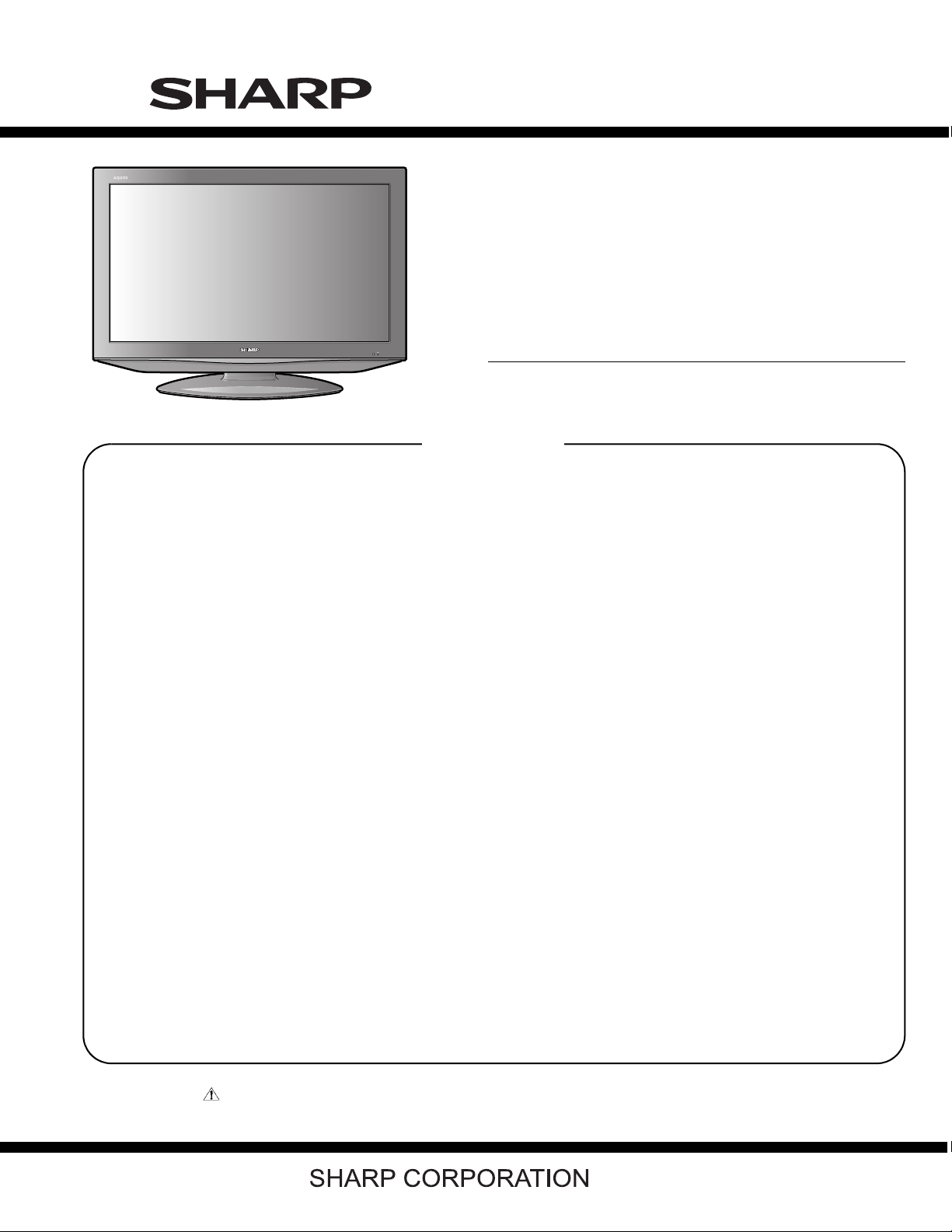
LC-37AD5E
SERVICE MANUAL
No. S77K9LC37AD5E
LCD COLOUR TELEVISION
CONTENTS
SAFETY PRECAUTION
IMPORTANT SERVICE SAFETY PRE-
CAUTION ............................................................i
Precautions for using lead-free solder ...............ii
CHAPTER 1. OPERATION MANUAL
[1] SPECIFICATIONS ......................................... 1-1
[2] OPERATION MANUAL .................................. 1-2
[3] DIMENSIONS ................................................ 1-7
CHAPTER 2. REMOVING OF MAJOR PARTS
[1] REMOVING OF MAJOR PARTS ................... 2-1
CHAPTER 3. ADJUSTMENT PROCEDURE
[1] After replacement of any PWB and/or IC for
repair, note the following. ............................... 3-1
[2] SOFTWARE UPDATING................................ 3-1
[3] Entering and exiting the adjustment pro-
cess mode.................................................... 3-16
[4] Remote controller key operation and de-
scription of display in adjustment process
mode. ........................................................... 3-16
[5] Adjustment process mode menu.................. 3-17
[6] Special features............................................ 3-18
[7] Video signal adjustment procedure.............. 3-19
[8] White Balance Adjustment ........................... 3-20
[9] Initialization to factory settings ..................... 3-21
[10] Lamp error detection .................................... 3-21
[11] Public Mode (Hotel Mode)............................ 3-22
MODEL
CHAPTER 5. MAJOR IC INFORMATIONS
[1] MAJOR IC INFORMATIONS .........................5-1
CHAPTER 6. OVERALL WIRING DIAGRAM/BLOCK
DIAGRAM
[1] OVERALL WIRING DIAGRAM ......................6-1
[2] MAIN BLOCK DIAGRAM...............................6-2
[3] SYSTEM BLOCK DIAGRAM .........................6-3
[4] POWER BLOCK DIAGRAM ..........................6-4
CHAPTER 7. PRINTED WIRING BOARD
[1] MAIN UNIT PRINTED WIRING BOARD........7-1
[2] AV UNIT PRINTED WIRING BOARD............7-5
[3] POWER UNIT PRINTED WIRING
BOARD.......................................................... 7-8
[4] D-TUNER UNIT PRINTED WIRING
BOARD........................................................7-10
[5] KEY UNIT PRINTED WIRING BOARD ....... 7-10
[6] DIGITAL UNIT PRINTED WIRING
BOARD........................................................ 7-11
[7] R/C, LED UNIT PRINTED WIRING
BOARD........................................................7-15
CHAPTER 8. SCHEMATIC DIAGRAM
[1] DESCRIPTION OF SCHEMATIC DIA-
GRAM............................................................8-1
[2] SCHEMATIC DIAGRAM................................8-2
Parts Guide
LC-37AD5E
CHAPTER 4. TROUBLESHOOTING TABLE
[1] TROBLESHOOTING TABLE ......................... 4-1
Parts marked with " " are important for maintaining the safety of the set. Be sure to replace these parts with specified ones for maintaining the
safety and performance of the set.
This document has been published to be used for
after sales service only.
The contents are subject to change without notice.
Page 2
LC-37AD5E
LC37AD5E
SAFETY PRECAUTION
Service Manual
IMPORTANT SERVICE SAFETY PRECAUTION
Service work should be performed only by qualified service technicians who are thoroughly familiar with all safety checks and the
servicing guidelines which follow:
WARNING
1. For continued safety, no modification of any circuit should be
attempted.
2. Disconnect AC power before servicing.
CAUTION:
FOR CONTINUED PROTECTION AGAINST A
RISK OF FIRE REPLACE ONLY WITH SAME
TYPE FUSE.
• Use an AC voltmeter having with 5000 ohm per volt, or higher, sensitivity or measure the AC voltage drop across the resistor.
• Connect the resistor connection to all exposed metal parts having a
return to the chassis (antenna, metal cabinet, screw heads, knobs
and control shafts, escutcheon, etc.) and measure the AC voltage
drop across the resistor.
All checks must be repeated with the AC cord plug connection
reversed. (If necessary, a nonpolarized adaptor plug must be used
only for the purpose of completing these checks.)
Any reading of 1.05 V peak (this corresponds to 0.7 mA peak AC.)
or more is excessive and indicates a potential shock hazard which
must be corrected before returning the monitor to the owner.
F701 (T4AL/AC250V)
BEFORE RETURNING THE RECEIVER
(Fire & Shock Hazard)
Before returning the receiver to the user, perform the following
safety checks:
3. Inspect all lead dress to make certain that leads are not pinched,
and check that hardware is not lodged between the chassis and
other metal parts in the receiver.
4. Inspect all protective devices such as non-metallic control knobs,
insulation materials, cabinet backs, adjustment and compartment
covers or shields, isolation resistor-capacitor networks, mechanical
insulators, etc.
5. To be sure that no shock hazard exists, check for leakage current in
the following manner.
• Plug the AC cord directly into a 220~240 volt AC outlet.
• Using two clip leads, connect a 1.5k ohm, 10 watt resistor paralleled by a 0.15µF capacitor in series with all exposed metal cabinet
parts and a known earth ground, such as electrical conduit or electrical ground connected to an earth ground.
///////////////////////////////////////////////////////////////////////////////////////////////////////////////////////////////////////////////////////////////////////////////////////////////////////////////////////////////////////////
TO EXPOSED
METAL PARTS
SAFETY NOTICE
Many electrical and mechanical parts in LCD color television have
special safety-related characteristics.
These characteristics are often not evident from visual inspection, nor
can protection afforded by them be necessarily increased by using
replacement components rated for higher voltage, wattage, etc.
Replacement parts which have these special safety characteristics are
identified in this manual; electrical components having such features
are identified by “ ” and shaded areas in the Replacement Parts
List and Schematic Diagrams.
///////////////////////////////////////////////////////////////////////////////////////////////////////////////////////////////////////////////////////////////////////////////////////////////////////////////////////////////////////////
For continued protection, replacement parts must be identical to those
used in the original circuit.
The use of a substitute replacement parts which do not have the same
safety characteristics as the factory recommended replacement parts
shown in this service manual, may create shock, fire or other hazards.
DVM
AC SCALE
1.5k ohm
10W
0.15µF
TEST PROBE
CONNECT TO
KNOWN EARTH
GROUND
i
Page 3
LC-37AD5E
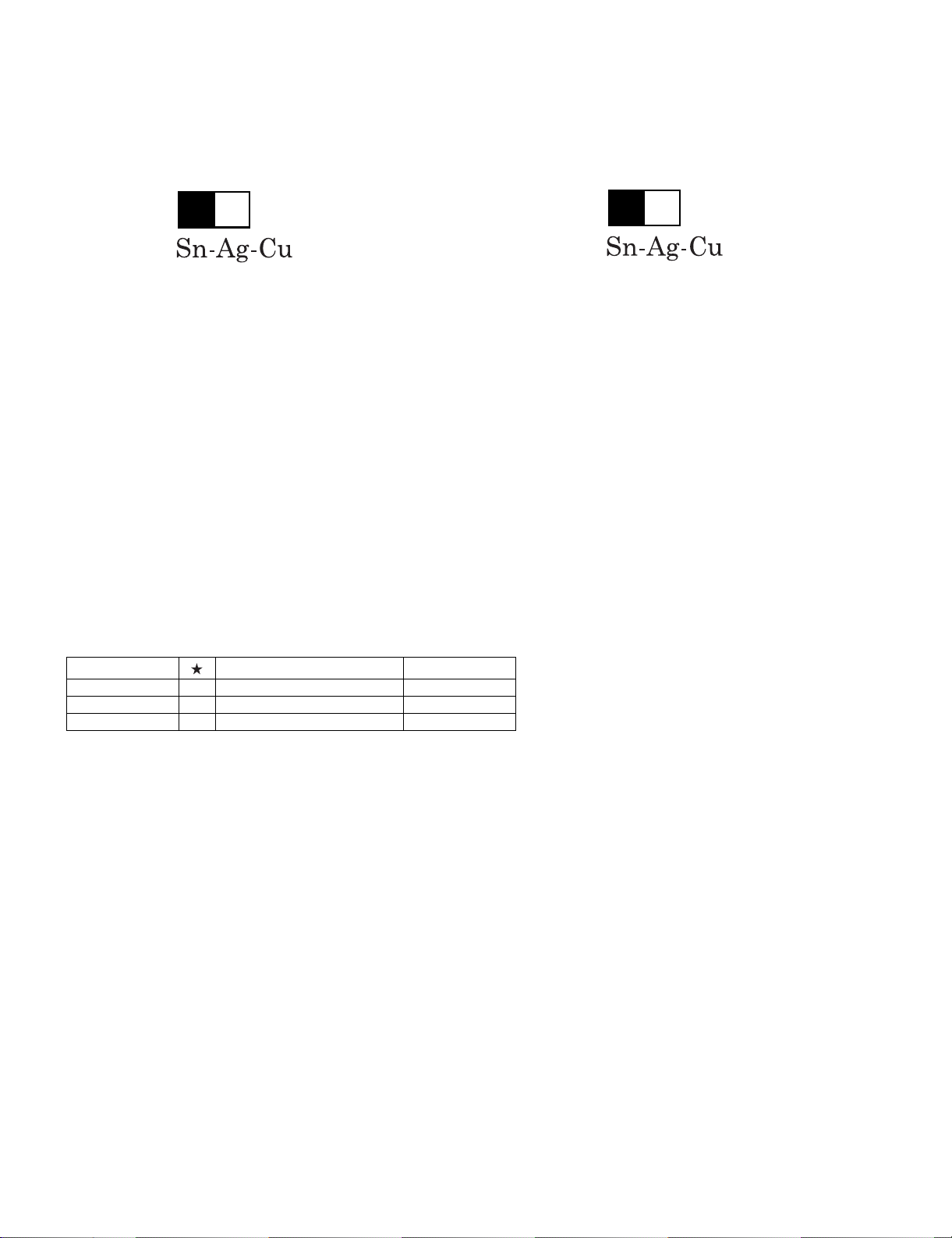
Precautions for using lead-free solder
Employing lead-free solder
• “PWBs” of this model employs lead-free solder. The LF symbol indicates lead-free solder, and is attached on the PWBs and service manuals. The
alphabetical character following LF shows the type of lead-free solder.
Example:
L Fa
Indicates lead-free solder of tin, silver and copper.
Indicates lead-free solder of tin, silver and copper.
L F a/a
Using lead-free wire solder
• When fixing the PWB soldered with the lead-free solder, apply lead-free wire solder. Repairing with conventional lead wire solder may cause damage or accident due to cracks.
As the melting point of lead-free solder (Sn-Ag-Cu) is higher than the lead wire solder by 40 °C, we recommend you to use a dedicated soldering
bit, if you are not familiar with how to obtain lead-free wire solder or soldering bit, contact our service station or service branch in your area.
Soldering
• As the melting point of lead-free solder (Sn-Ag-Cu) is about 220 °C which is higher than the conventional lead solder by 40 °C, and as it has poor
solder wettability, you may be apt to keep the soldering bit in contact with the PWB for extended period of time. However, Since the land may be
peeled off or the maximum heat-resistance temperature of parts may be exceeded, remove the bit from the PWB as soon as you confirm the
steady soldering condition.
Lead-free solder contains more tin, and the end of the soldering bit may be easily corroded. Make sure to turn on and off the power of the bit as
required.
If a different type of solder stays on the tip of the soldering bit, it is alloyed with lead-free solder. Clean the bit after every use of it.
When the tip of the soldering bit is blackened during use, file it with steel wool or fine sandpaper.
• Be careful when replacing parts with polarity indication on the PWB silk.
Lead-free wire solder for servicing
Part No. Description Code
ZHNDAi123250E J φ0.3mm 250g (1roll) BL
ZHNDAi126500E J φ0.6mm 500g (1roll) BK
ZHNDAi12801KE J φ1.0mm 1kg (1roll) BM
ii
Page 4
LC-37AD5E
LC37AD5E
CHAPTER 1. OPERATION MANUAL
[1] SPECIFICATIONS
Service Manual
urkis h/Gr
1 – 1
Page 5
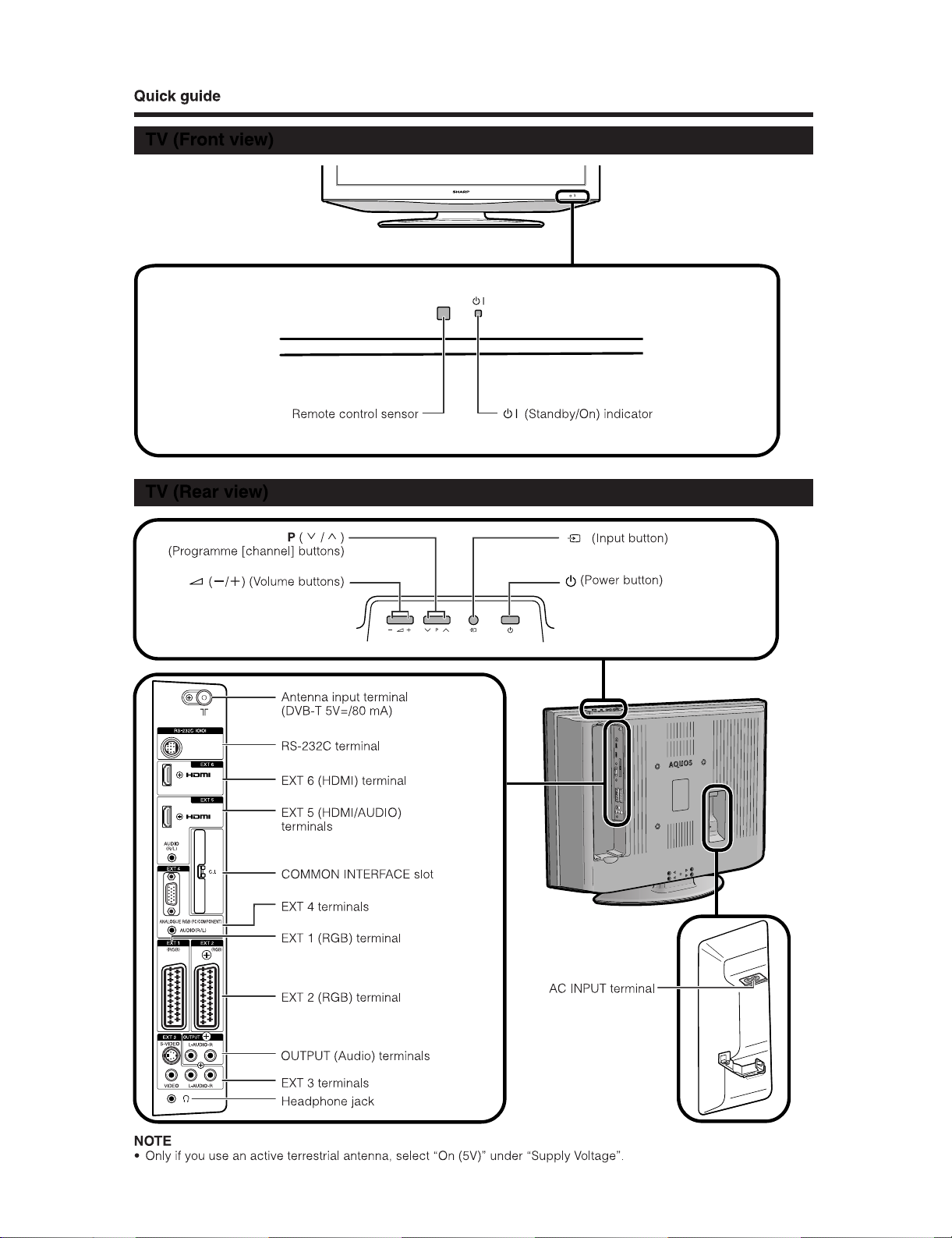
[2] OPERATION MANUAL
LC-37AD5E
1 – 2
Page 6
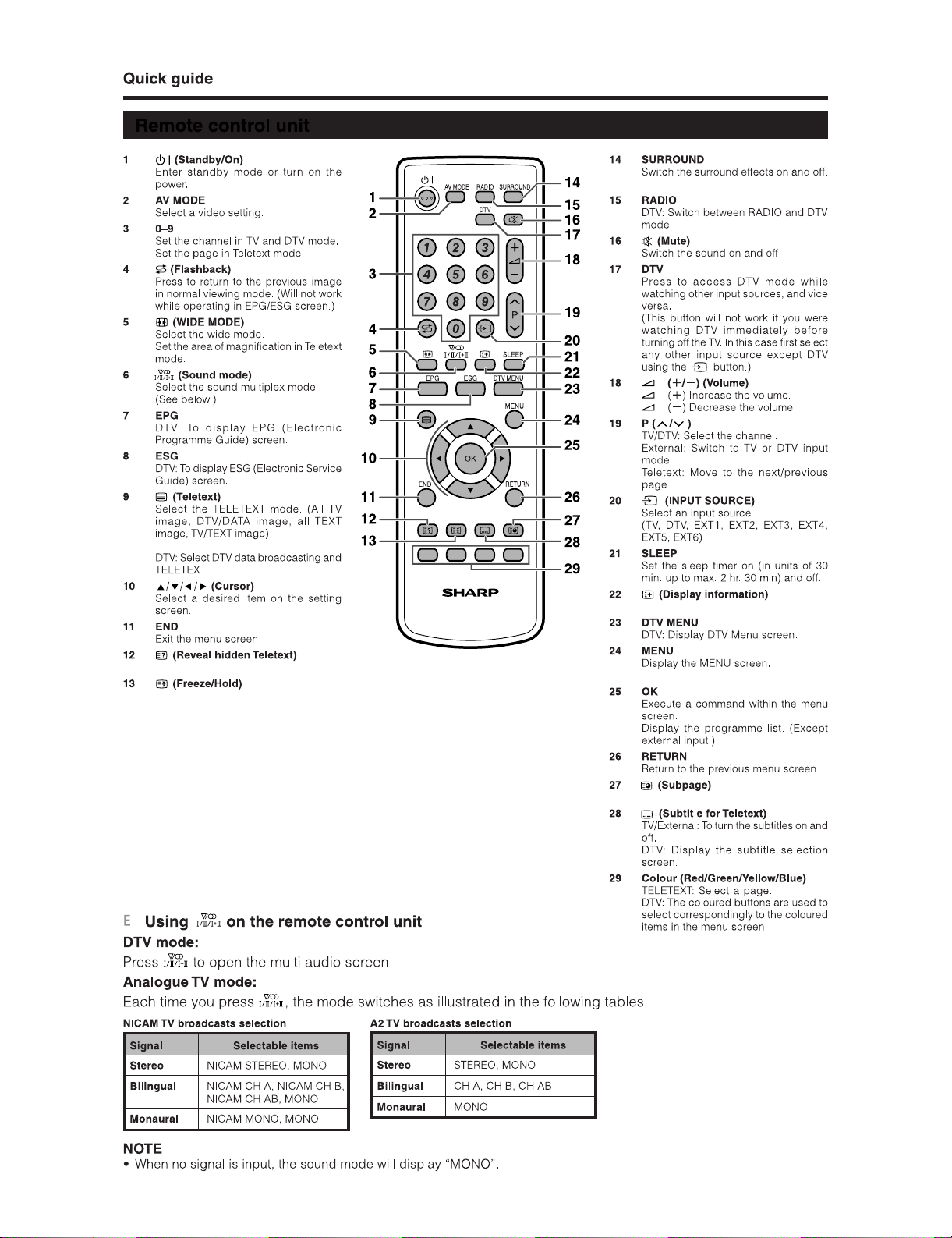
LC-37AD5E
1 – 3
Page 7
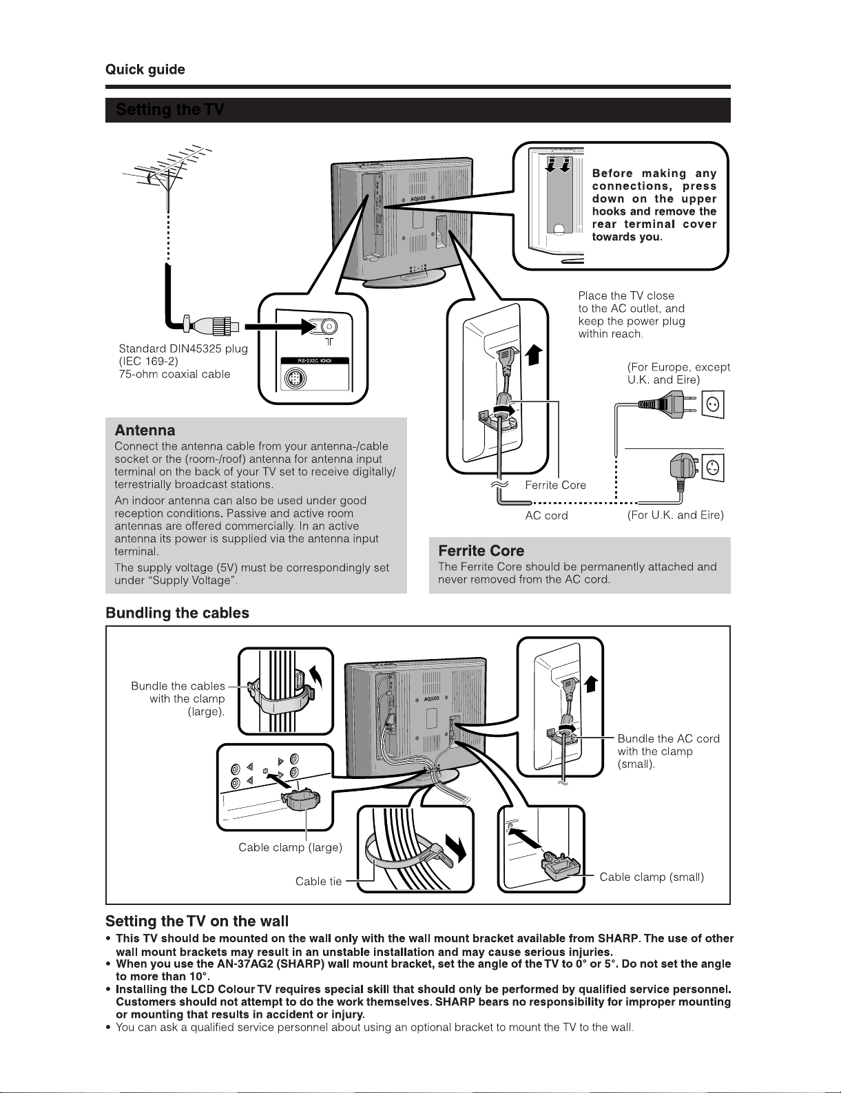
LC-37AD5E
1 – 4
Page 8
LC-37AD5E
1 – 5
Page 9
LC-37AD5E
1 – 6
Page 10
LC-37AD5E
[3] DIMENSIONS
Units: inches (mm)
919.0
822.6
650.5
601.5
463.8
370.4
49.0
547.0
200.0
293.0
116.5114.8
85.0
200.0
1 – 7
Page 11
Set each holder like this way.
Others are omitted .
#LCD HOLDER Set to gide lib of CAB-A
Push untill Locked
LC37AD5E
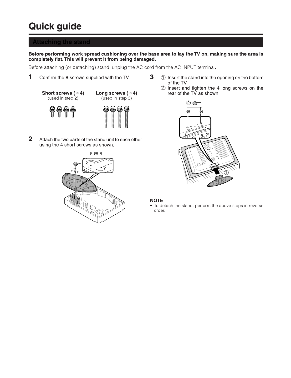
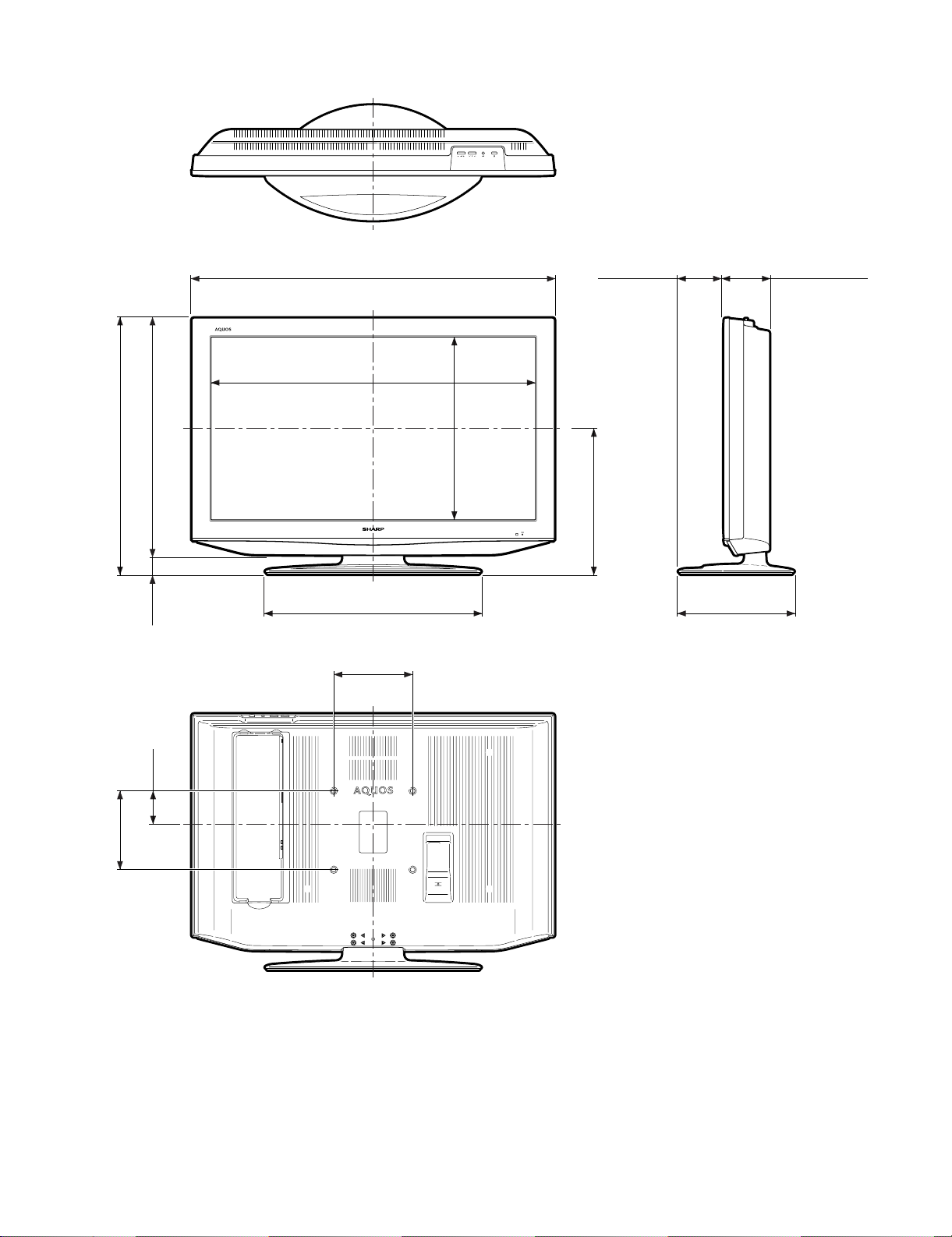
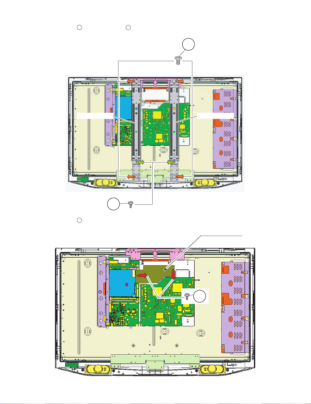
CHAPTER 2. REMOVING OF MAJOR PARTS
Service Manual
[1] REMOVING OF MAJOR PARTS
LC-37AD5E
1. Remove the 4 lock screws , and the 12 lock screws . Detach the Rear Cabinet.
1
2
2
1
Rear Cabinet
2. Remove the 6 lock LCD Side Holders .
3
3
3
3
3
3
3
2 – 1
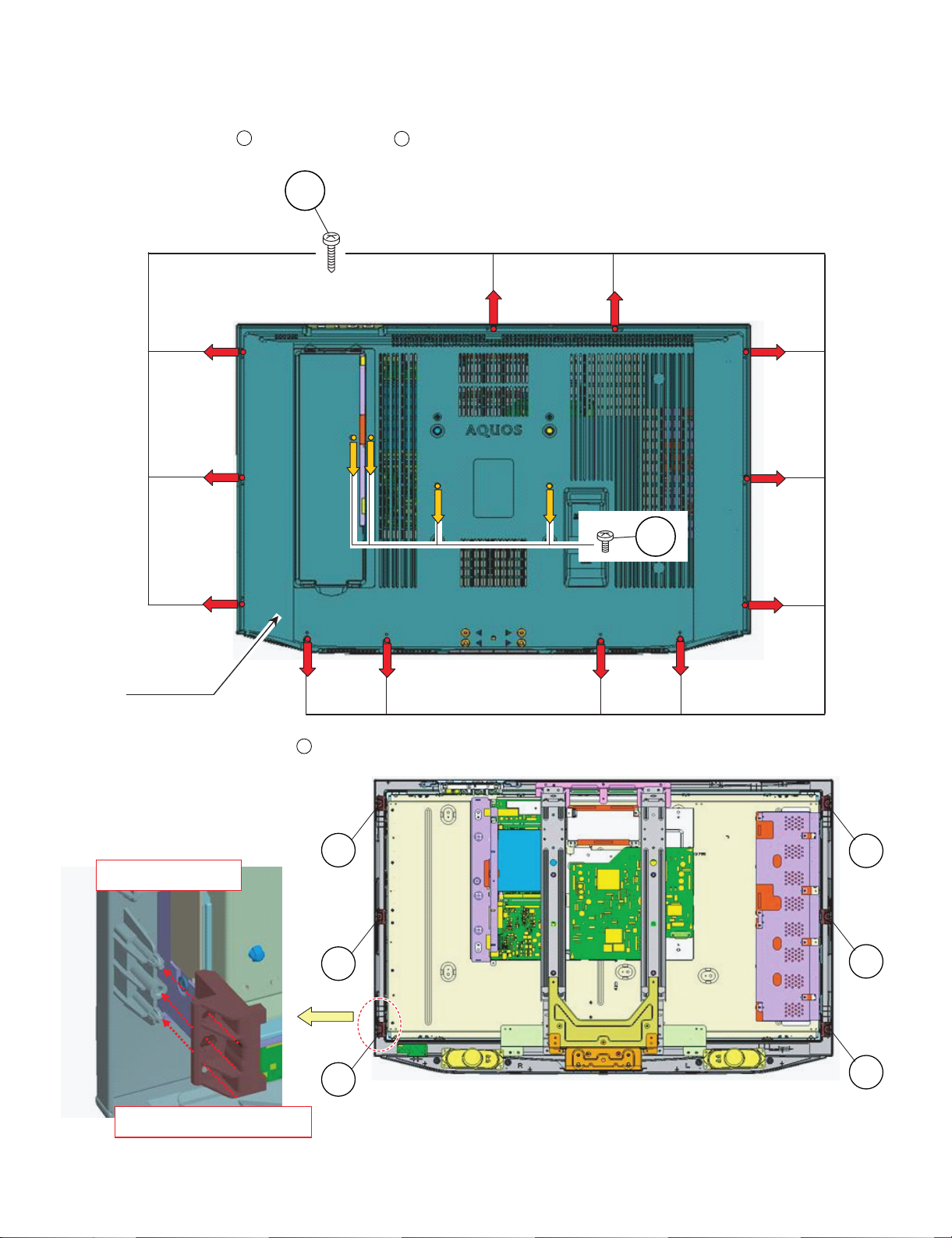
Page 12
LC-37AD5E
STAND ANGLE UNIT
Wire "KM" to WH
3. Remove the 9 lock screws . Detach the Stand Angle Unit.
4
4
4. Remove the 2 lock screws . Detach the Top Control Cover Ass'y.
TOP CONTROL COVER
Wire "KM"
5
TOP CONTROL COVER ASS'Y
5
2 – 2
Page 13
LC-37AD5E
5. Remove the 2 lock scrwes , and the 4 lock screws . Detach the Center Angle-L/R.
6
7
7
CENTER ANGLE LCENTER ANGLE R
6
6. Remove the 2 lock scrwes . Detach the Digital Shield.
8
DIGITAL SHIELD
8
2 – 3
Page 14
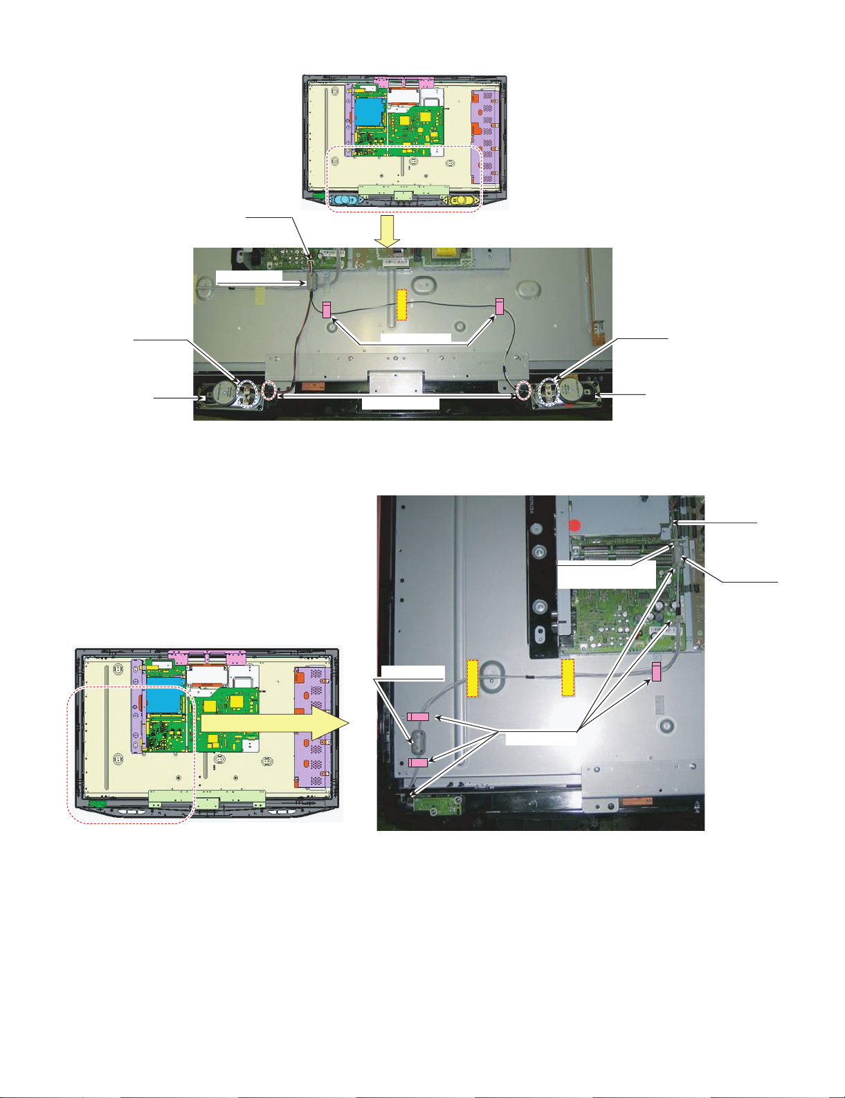
LC-37AD5E
FOR Wire "SP"
Wire "SP" to SP Lib
Wire "SP" to WH
FOR Wire "RA"
#StoptomoveCore,
No shape to Shield A ngle
Wire "RA" to WH
7. Remove all the connectors from PWBs.
Wire "SP"
Wire "SP-R"
SP-R
Wire "SP-L"
SP-L
Wire "RA"
for "RA" wire
2 – 4
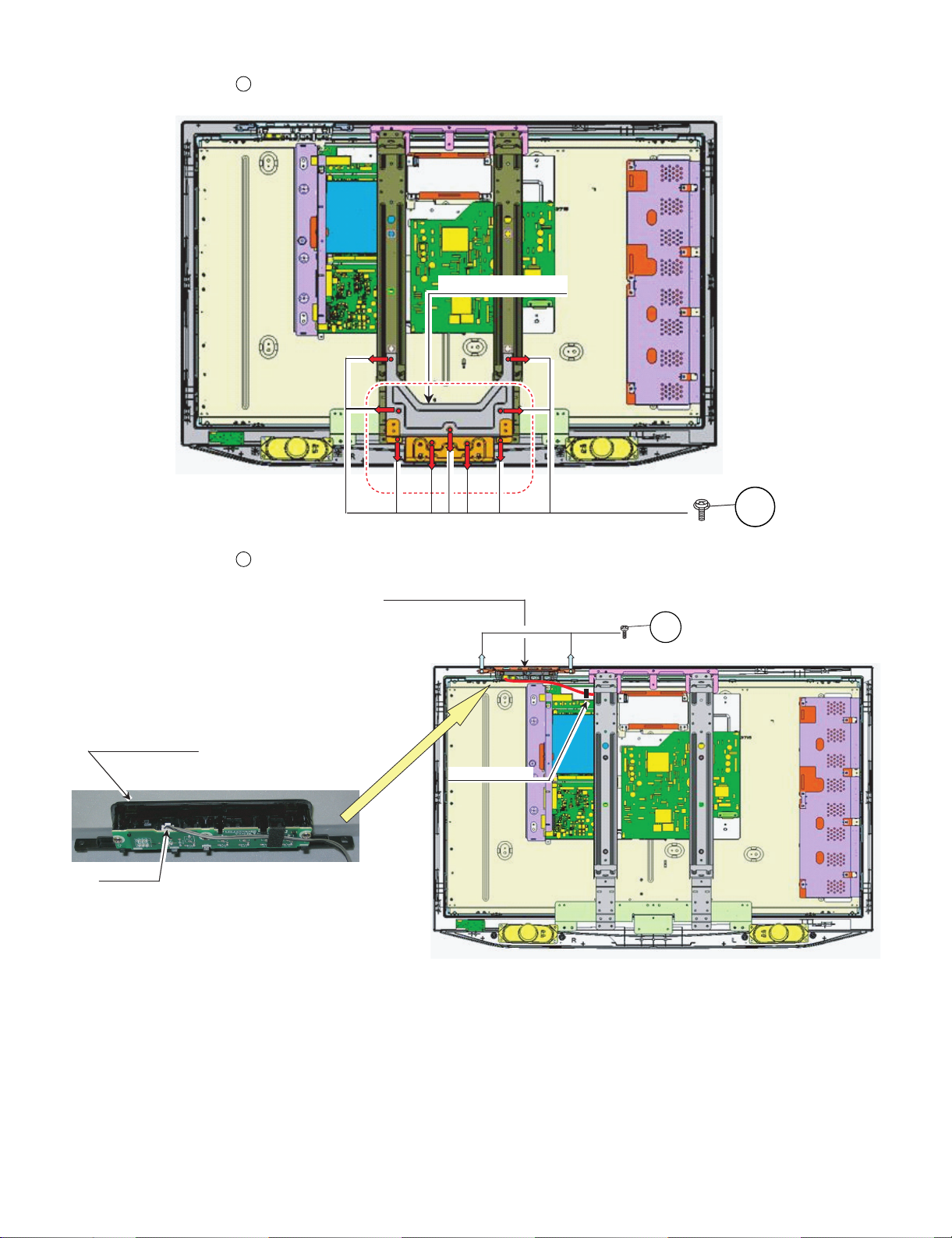
Page 15
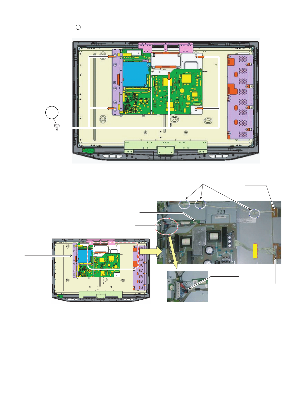
LC-37AD5E
8. Remove the 5 lock screws . and detach the Chassis Tray Unit.
9
9
9. Remove all the connectors from PWBs.
Chassis Tray Unit
Wire "SH"
Wire "LV"
Wire "LB" to WH
Wire "LB"
Wire "LV" to WH
Wire "LA"
2 – 5
Page 16
LC-37AD5E
Tuner Unit
10.Remove the 1 lock screw . Detach the Terminal Cover.
11.Remove the 2 lock screws . Detach the D-Tuner Unit.
10
11
11
D-TUNER Unit
B to B connector
10
Chassis Tray Unit
2 – 6
Page 17
LC-37AD5E
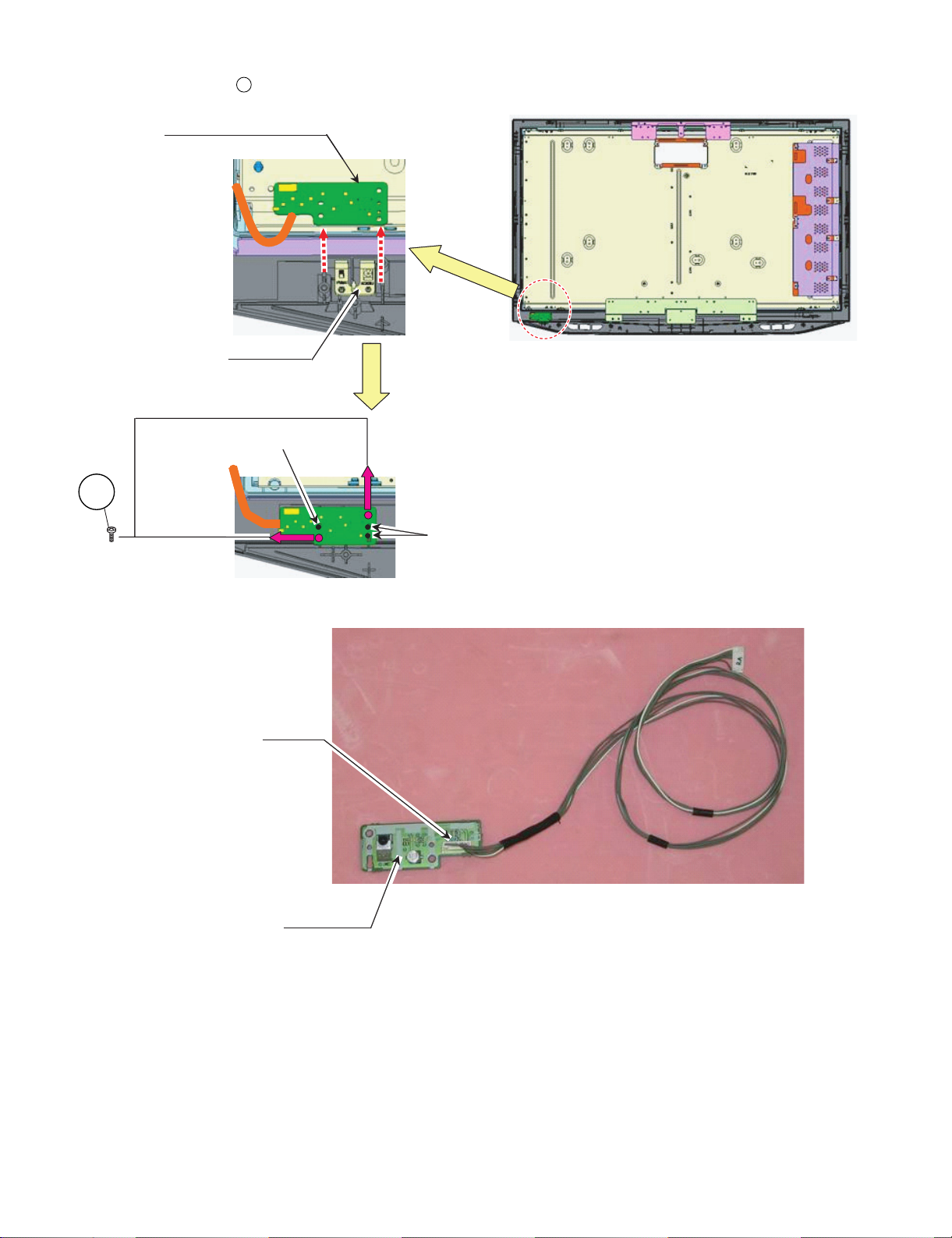
12.Remove the 2 lock screws . Detach the R/C, LCD Unit.
R/C LED UNIT With Wire "RA"
Wire "RA"
#R/C LED PWB Set to gide lib of CAB-A
Wire "RA"
12
LED COVER
12
Wire "RA"
R/C, LED UNIT
#R/CLEDPWBSettogidelibofCAB-A
2 – 7
Page 18
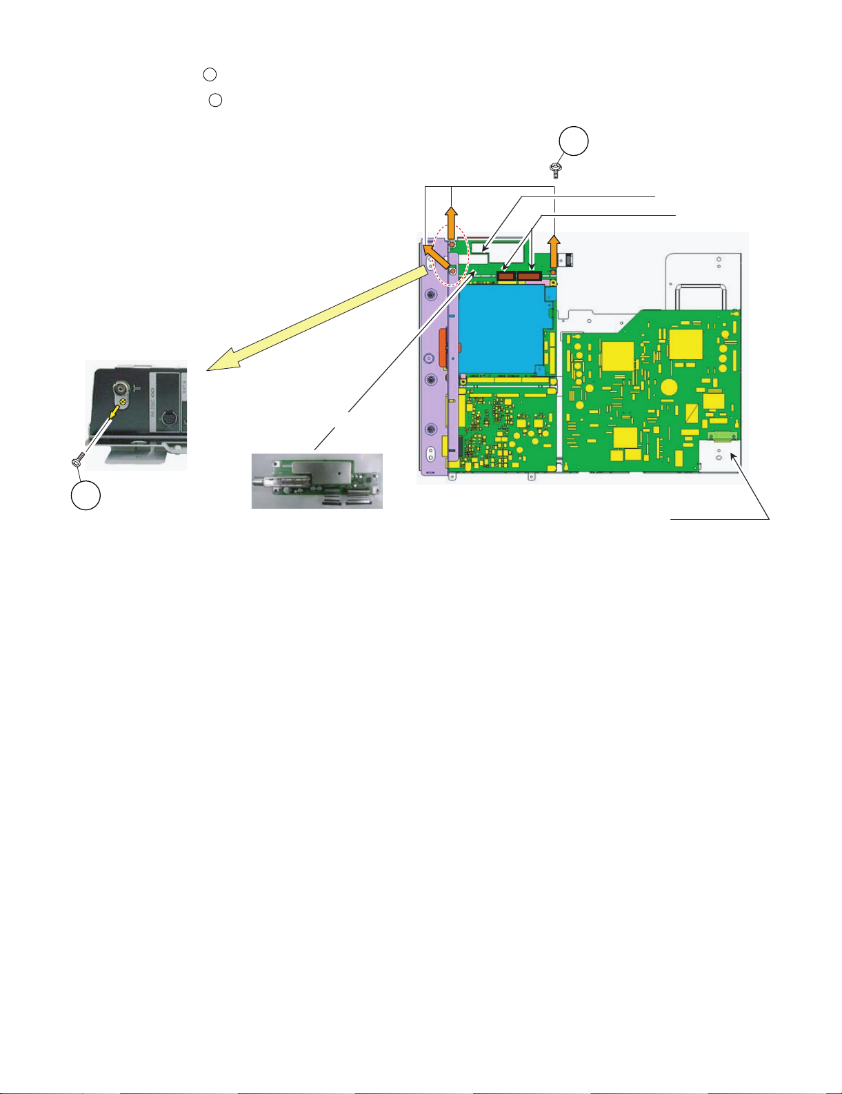
LC-37AD5E
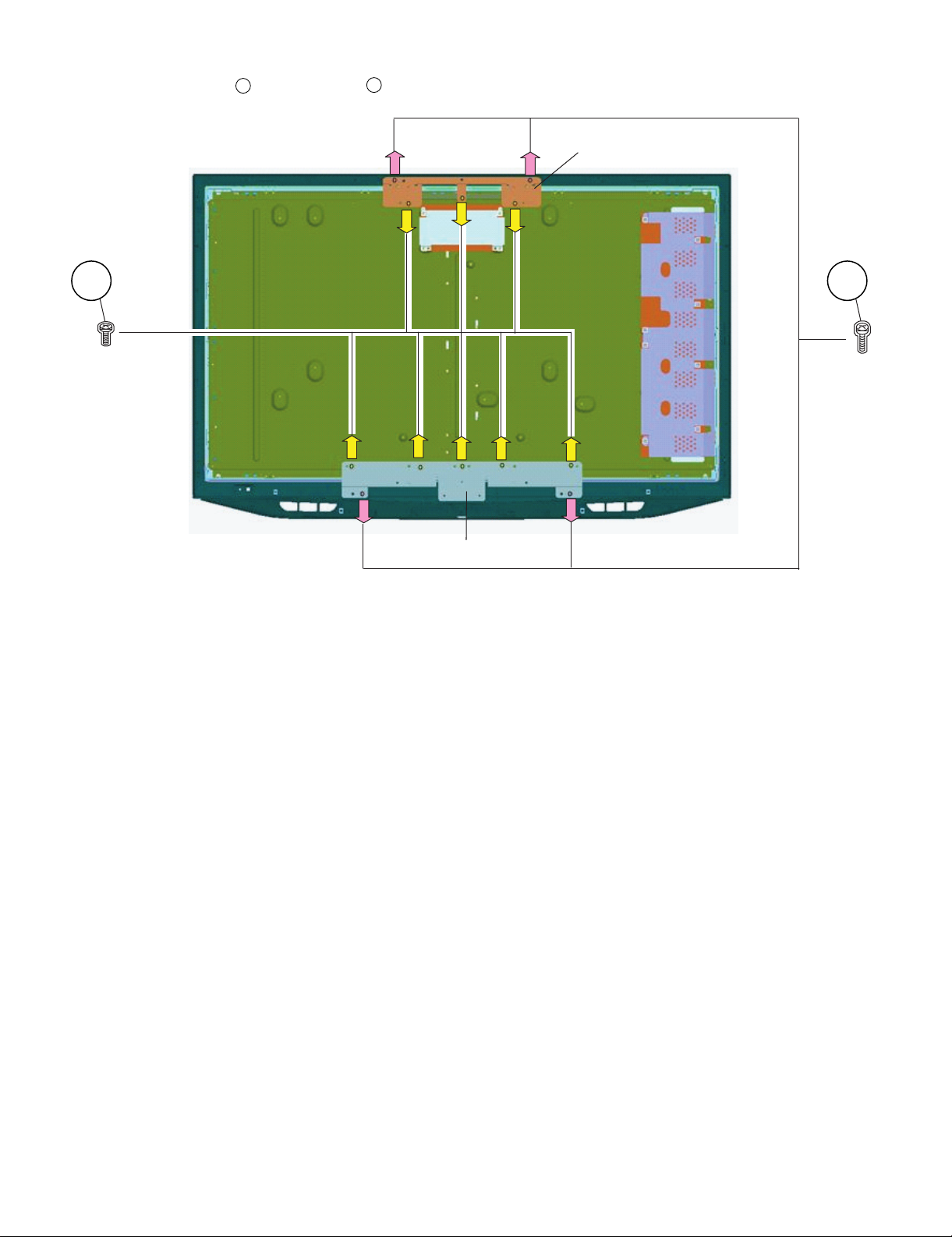
13.Remove the 4 lock screws , and 8 lock screws . Detach the LCD Angle.
13
14
LCD ANGLE TOP
14 13
LCD ANGLE BOTTOM
2 – 8
Page 19
LC37AD5E
CHAPTER 3. ADJUSTMENT PROCEDURE
Service Manual
[1] After replacement of any PWB and/or IC for repair, note the following.
When replacing the following units, be sure to prepare the new units loaded with updated software.
MAIN-UNIT: DUNTKD890FM32
• Note that an IC into which ROM data is written is available for MAIN-UNIT servicing (see below)
IC1901 VHi24LC2BiNEES EDID (HDMI)
IC1902 RH-iXC023WJZZS EDID (HDMI)
IC2303 RH-iXB731WJZZS EDID (PC)
[2] SOFTWARE UPDATING
There are 2 methods to update software in the VCTp: I2C method, RS-232C HyperTerminal and RS-232C Tera Term method.
• RS-232C method is allowed when the TV is working properly and the action should be only software upgrade.
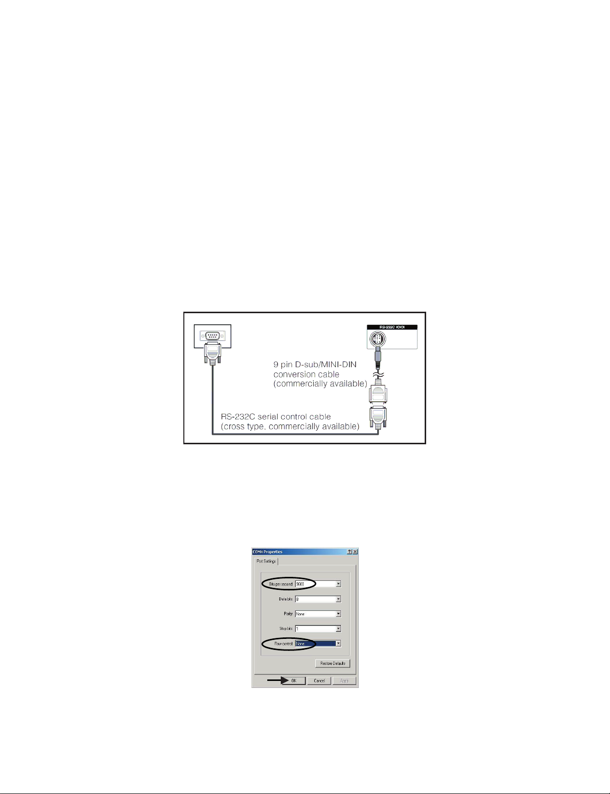
1. RS-232C Method Description (HyperTerminal).
The hardware tools requirement are:
1. A Modem-null (Cross type) DB9 female to DB9 female cable.
2. An adaptor DB9 male to mini-Din 9 pin male cable (Sharp Code: QCNWGA015WJPZ)
3. Make the connections as indicated in the figure:
LC-37AD5E
Computer TV set
Before using RS-232C updating method is necessary to configure a Terminal PC software. HyperTerminal has been selected as a Terminal software because it’s include in all Windows versions as an accessory, and you can find it inside “Accessories\Communications” folder. For this reason, please follow carefully the next steps:
1) First time HyperTerminal is used, it’s necessary to configure some settings. Follows next action to configure two connection: low speed
(9600bps) and high speed (115200bps).
2) Create a New Connection file with name “P55_9600bps”.
3) Select a free COM port and select the Port Settings properties as follows:
3 – 1
Page 20
LC-37AD5E
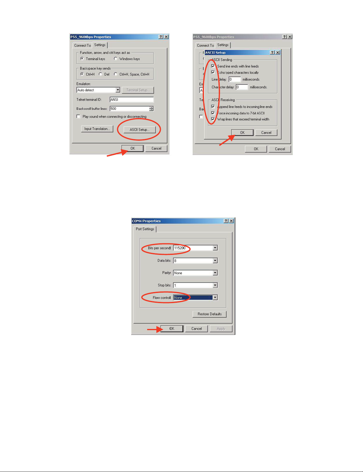
4) Click on “File\Properties” menu for selecting the General and ASCII properties as follows:
5) Select “New Connection” in the File Menu.
6) Answer “Yes” to close current connection and “Yes” to save session “P55_9600bps”.
7) Create a new connection with the name “P55_115200bps”.
8) Select a the same COM port used in item 2 and select the Port Settings properties as follows:
9) Select the same General and ASCII properties as item 3.
10)Close HyperTerminal session, answering “Yes” to close current connection and “Yes” to save session “P55_115200bps”.
To start updating session, click over “P55_9600bps” icon that you can find in the “START\All programs\Accessories\ Communications\HyperTerminal\HyperTerminal” folder and follow next procedure:
3 – 2
Page 21
LC-37AD5E
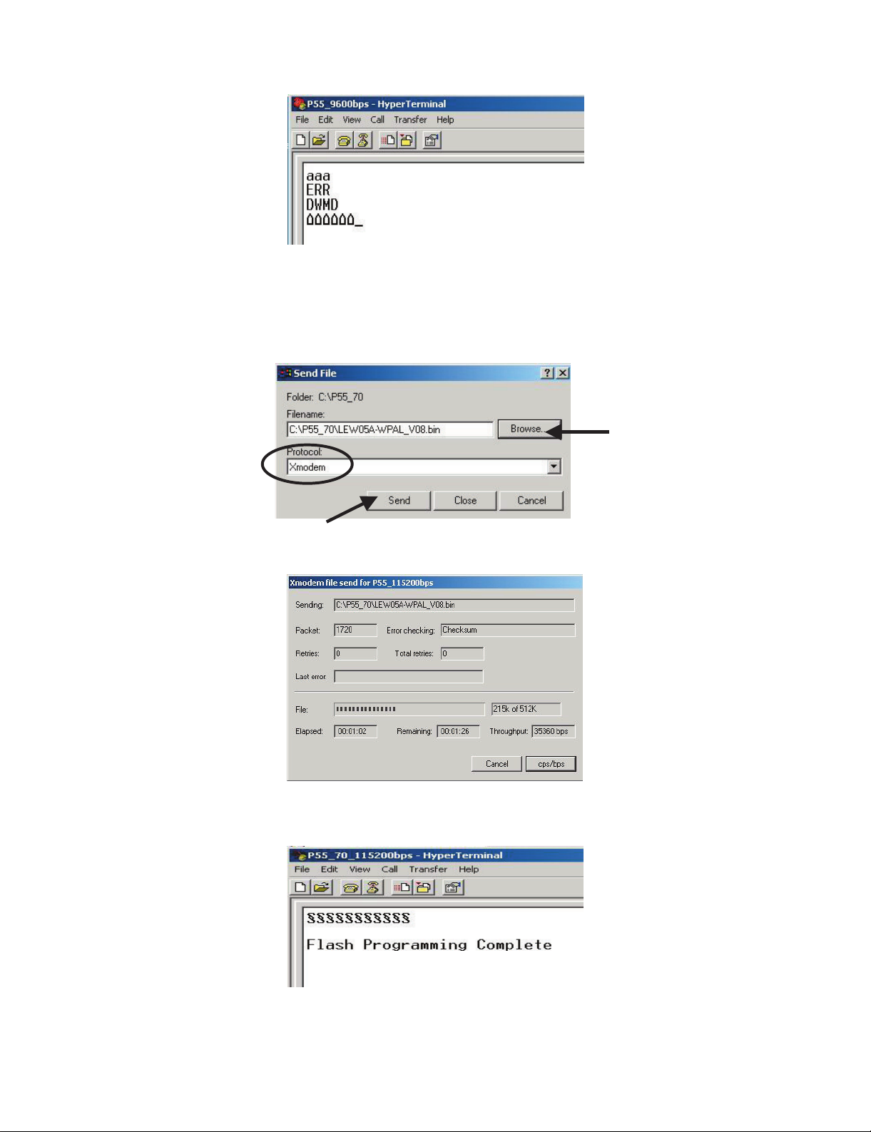
1) Check the connection between TV set and PC, sending a wrong command, as for example: “aaa”. TV set returns an “ERR” label as an syntaxis
ERROR (Not correct order or sequence).
2) Send the command “DWMD” to enter TV set in Download Mode. The TV set answer sending same symbol continuosly. If this symbol character
doesn’t appear, please don’t worry and pass to next step.
3) Close this connection and open “P55_115200bps” connection clicking over the “P55_115200bps” that you can find in “START\All pro-
grams\Accessories\ Communications\HyperTerminal\HyperTerminal” folder.
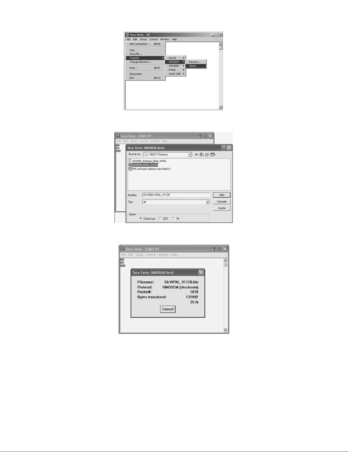
4) Using “Transfer\Send file...” menu, select desired file (.bin format) and the transmission protocol (Xmodem) as show below.
5) After press “Send” button the updating process starts as follows:
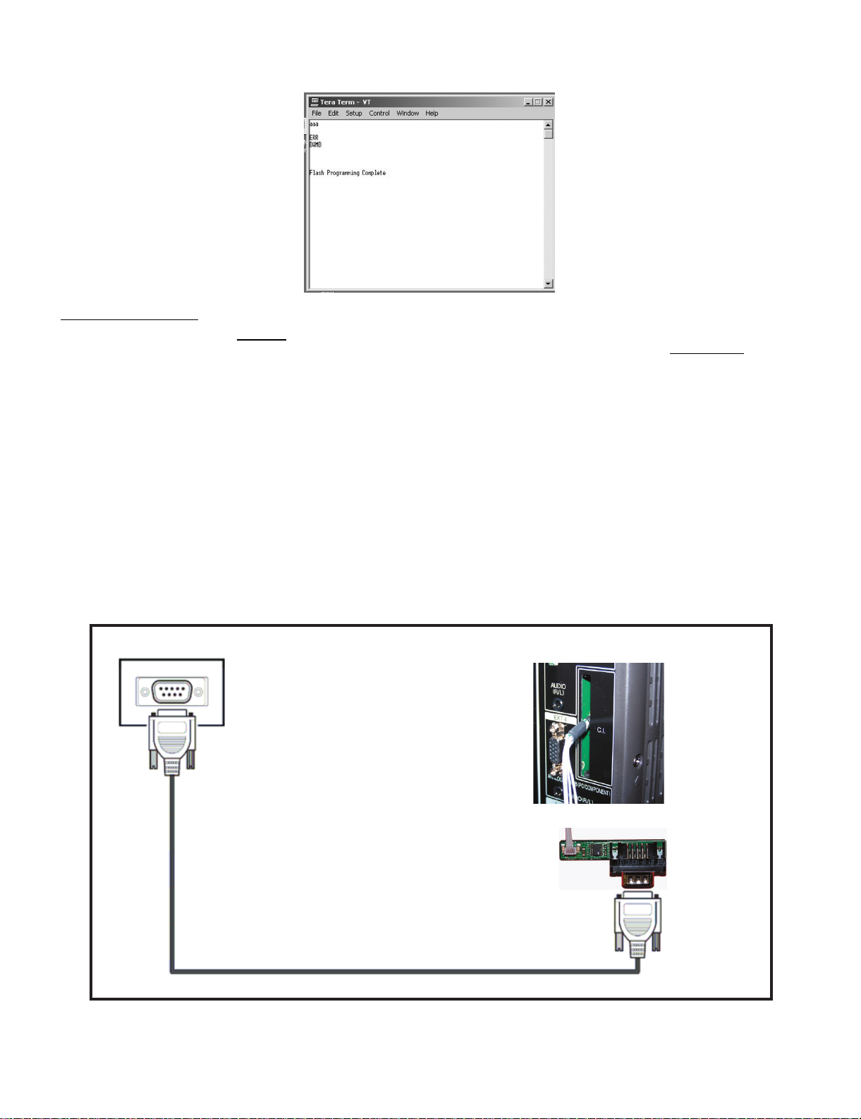
6) When flash update process finishes, the “Flash Programming Complete” label appears in the screen, the device automatically go to switch off,
and in a few seconds go to switch on again.
VERY IMPORTANT NOTE:
During the updating time, please don’t use the PC for other purpouses, in order to abolish communication problems between TV set and
PC. If TV set was not updated properly, the TV won’t have the software to startup again, and you must follow the “I2C method” to update
another time the TV set.
3 – 3
Page 22
LC-37AD5E
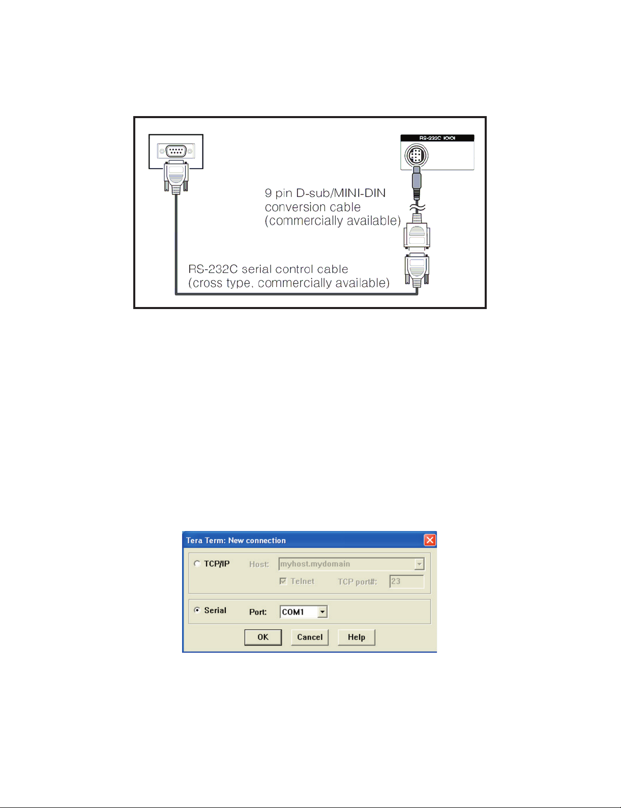
2. RS-232C Method Description (Tera Term)
The hardware tools requirement are:
1. A Modem-null (Cross type) DB9 female to DB9 female cable.
2. An adaptor DB9 male to mini-Din 9 pin male cable (Sharp Code: QCNWGA015WJPZ)
3. Make the connections as indicated in the figure:
Computer TV set
Software requirements:
To upgrade VCTp software from RS-232C external connector is necessary to use a Tera Term (Pro) free software.
The URL of Tera Term home page is:
http://hp.vector.co.jp/authors/VA002416/teraterm.html
(The address may be changed in future)
Tera Term (Pro) supported operating systems:
MS-Windows 95 or upper
MS-Windows NT 3.5 and 4.0 or upper
Note.- For Windows 3.1 use Tera Term version 1.X.
Copy all the distribution files to an empty floppy disk or temporary directory (for example C:\ TEMP).
Run SETUP.EXE and follow the instruction given by it.
After the installation, the distribution? les are no longer needed, you can delete them or may keep them in the floppy disk.
Ho w to us e Tera Te r m Pro:
When the Tera Term (Pro) program is used, it’s necessary to shape some settings. Follows next action to configure the connection:
3 – 4
Page 23
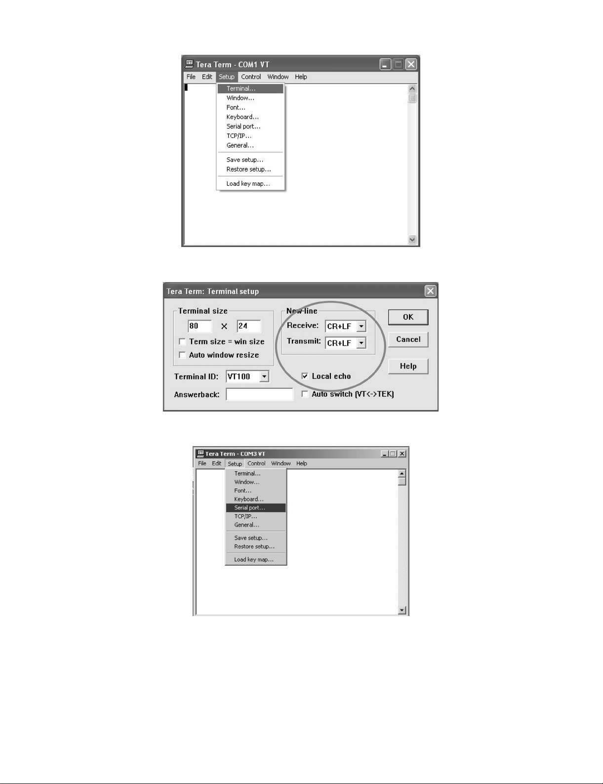
1) Select: Serial→COM X→ O.K.
2) Select: Term inal
LC-37AD5E
3) Choose the same options as the above picture.
3 – 5
Page 24
LC-37AD5E
4) Select: Setup → Serial port → O.K. Appear the follow screen:
5) Select follows settings:
Serial port to use: COM x
Baud rate: 9600
Data: 8 bits
Parity: none
Stop: 1 bit
Flow control: none
Enter O.K.
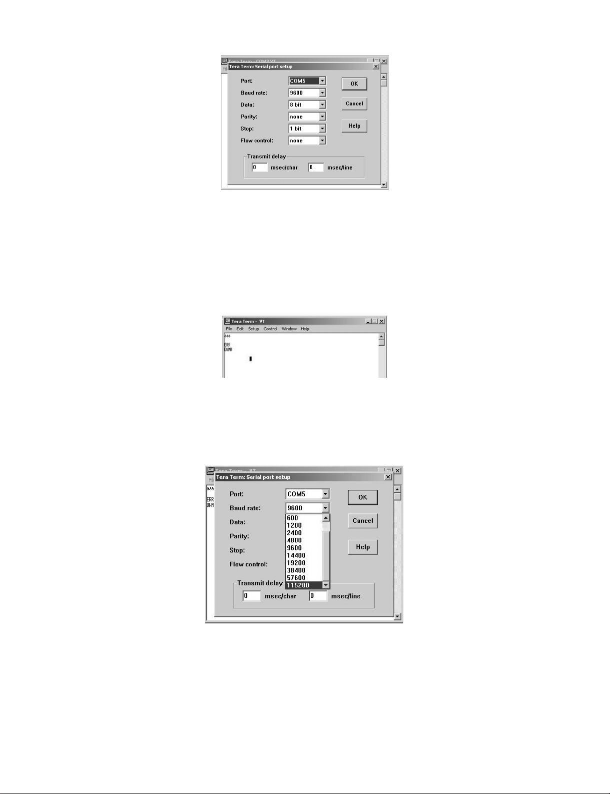
6) Check the connection between TV set and PC, sending a wrong command, as for example: “aaa”. TV set returns an “err” label as an syntaxes
ERROR (Not correct order or sequence).
Send a “DWMD” (capital letters) command to enter TV set in Download Mode.
Change a baud rate to 115200.
Select: Setup → Baud rate → 115200 → O.K.
3 – 6
Page 25
7) Select: File → Transfer → XMODEM → Sent
8) Choose the file for upgrade and click “Open”.
LC-37AD5E
9) After select “Open” the upgrade process starts as follows:
3 – 7
Page 26
LC-37AD5E
10)When flash update process finishes, the “Flash programming complete” label appear in the screen, the device automatically go to switch off, and
in a few seconds go to switch on again.
VERY IMPORTANT NOTE:
During the updating time, please don’t use the PC for other purposes, in order to abolish communication problems between TV set and PC.
If TV set was not updated properly, the TV won’t have the software to startup again, and you must follow the “I2C method”
another time the TV set.
3. How to update the Digital Board Software.
There are 2 methods to update the Digital Board Software on Flash Memory (IC4203) thought the Digital Processor (IC4001).
• Jig RS-232 Method (From PC trough RS-232C COM port).
• PCMCIA CARD (Compact Flash Memory) Method.
NOTE: The PCMCIA method is only compatible with those PCs running XP Windows Version.
to update
3.1. Jig RS-232 Method Description
• Hardware requirements:
1. A modem null (Cross type) DB9 female to DB9 female cable.
2. The Jig Kit (Sharp Code: QCNWKA012WJZZ)
3. Make the connections as in the below figure.
Computer
TV Set
(CI Terminal)
~
~
Jig
RS-232C serial control cable
(cross type, commercially available)
• Software requirements:
1. “Winupload” application software on PC.
3 – 8
Page 27
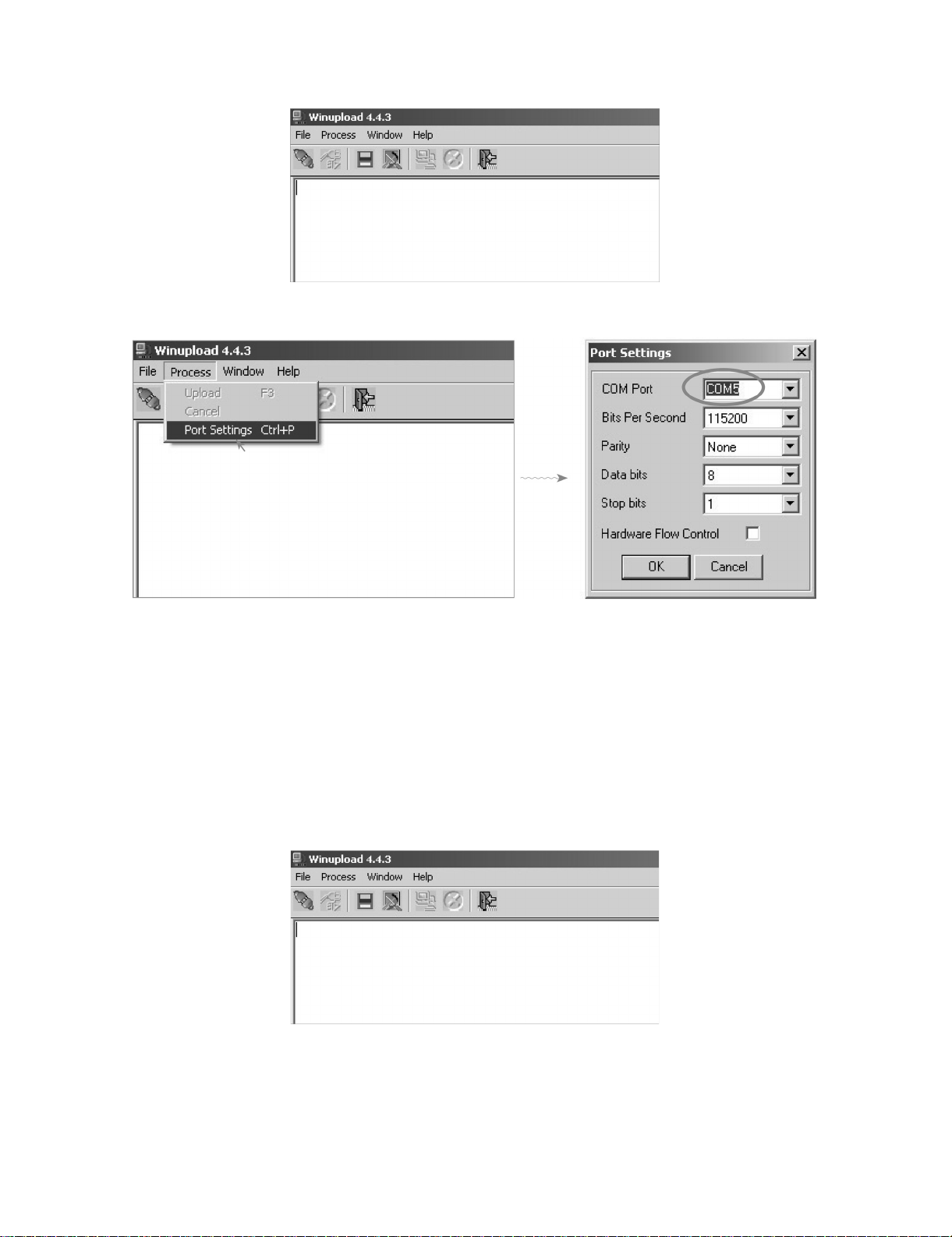
• How to setup the “Winupload” software for the first time:
1. Start “Winupload”. It will appear the following picture.
2. Select the most suitable RS232 Serial Port from “Port Setting” - “Process” Menu.
LC-37AD5E
3. Select the following settings from “Port Settings” Menu.
Bits Per Second: 115200
Parity: None
Data bits: 8
Stop bits: 1
Hardware Flow Control: OFF
• Procedure for updating the TV set.
1. Switch off the TV set to be updated, in DTV mode.
2. Start “Winupload”. It will appear the following picture on PC.
3 – 9
Page 28
LC-37AD5E
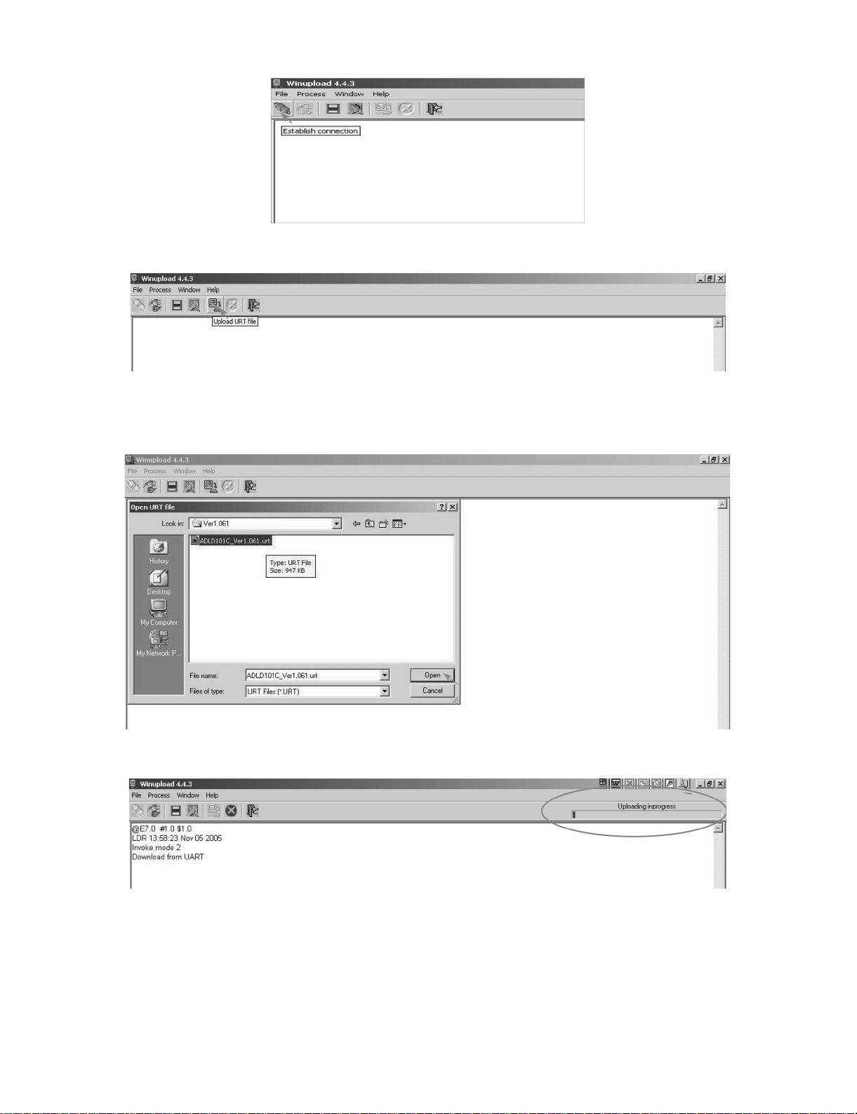
3. Establish connection on Winupload Software.
4. Select “Upload URT file”
5. Select and open the “.urt” data file from data directory
NOTE: Consider the version shown below just an example, may be is not the latest one, and could be different depending on the TV set destination
(market/Country) or model.
6. Switch On the TV Set (previously in DTV Mode). The Uploading Process starts automatically.
3 – 10
Page 29
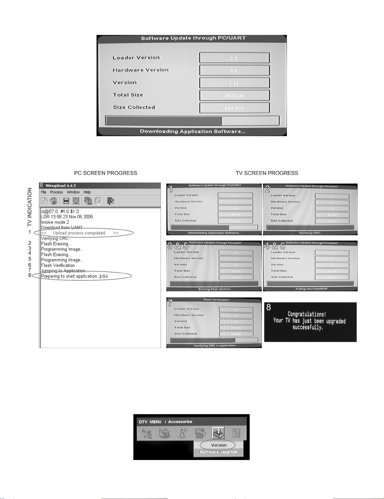
LC-37AD5E
While the TV set is uploading the software, the following information is shown on the TV set screen.
Then, data transfer from PC to TV set finishes when the “Upload progress completed” label appears in the “Winupload” screen. Now, the TV set made
some additional verification (Items #2 to #7). When the full uploading process is finished, in the “Winupload” window appears the label “Preparing to
start application” for a new TV Set, and just now, in the TV screen of the updated set, appears a congratulations label (Item #8).
NOTE: Do not turn off the TV set while the software updating was in progress.
7. Unplug the AC cord.
8. Disconnect the Jig from TV Set.
• Software Version verification procedure.
1. Connect the AC cord and Switch On the TV Set.
2. Select DTV Menu on TV Set. The following On Screen Display will appear.
3 – 11
Page 30
LC-37AD5E
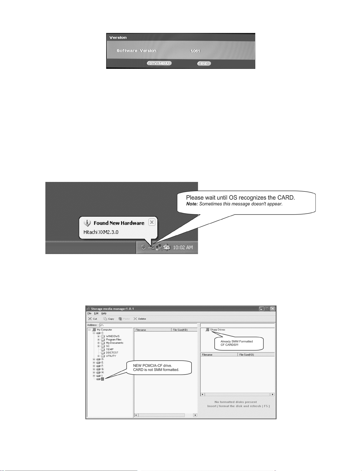
3. Select “Version”. The updated version can be verified.
NOTE: Consider the version shown above just as example, may be is not the latest one, and could be different depending on the TV set destination
(market/Country) or model.
3.2. PCMCIA Card (Compact Flash) Method.
• Hardware requirements:
1. Compact Flash Memory Card.
2. PCMCIA Compact Flash Adapter or USB Multi Card Reader.
• Software requirements:
1. “StorageMediaManager1.0.1” application software, installed on PC.
2. “Loader 1.1” or higher application software, installed on DTV Set.
NOTE: Storage Media Manager only for Windows XP.
• How to prepare the CF Card using the “Storage Media Manager 1.0.1” (SMM):
1. Insert PCMCIA (Compact Flash (CF) + CF-Adapter)
2. Execute SMM. If SMM does not appear or a Windows Error Box appears, please verify there are no USB media drives connected to the PC.
NOTE: Consider that it's recommended remove unnecessary media during SMM execution. Probably, If you try to use an USB Multi Card Reader
with SMM doesn't work fine.
3. If the CF card has never been formatted for the SMM (is not same format type used in Windows), the SMM will show you the PCMCIA-CF drive as
a Windows Media Drives, hanged of the “My Computer” tree (“J” Drive in the picture showed below).
But, if the PCMCIA-CF card had been formatted previously by SMM, directly the PCMCIA-CF drive will appear in the SMM formatted Drives box
(Sharp Drives). Please go to Item #6.
3 – 12
Page 31

4. In case of not SMM formatted card, select PCMCIA-CD Drive and using the Right-Click Pop up Menu please format the Drive.
5. Formatting the CF card. Select “Yes” to confirm the action.
NOTE: All FC’s data of the inside are erased.
LC-37AD5E
6. If SMM formatted card already appears under SHARP DRIVES box please continue, if not try to repeat from item #1. Select origin folder and “.img”
data file to be written in the CF card.
3 – 13
Page 32

LC-37AD5E
7. First of all, select copy target drive and then use Drag & drop for the “.img” file.
8. Wait, copy is in process.
9. Copy is finished, when the Copying progress bar disappears and the name of data file appears in the File Box.
3 – 14
Page 33

LC-37AD5E
10. Close SMM application.
11. Remove PCMCIA safely using the Windows Task bar pop up menu (Right-click over the Tray Icon).
12. Now, the PCMCIA-CF card is prepared to update the TV set.
Procedure to update the TV Set using PCMCIA-CF Card:
1. Switch Off the LCD TV Set in DTV mode.
2. Insert PCMCIA Card (already prepared according the details before given at “How to prepare the CF Card using the “Storage Media Manager
1.0.1 “(SMM))”.
3. Switch On the LCD TV Set (it starts automatically the updating, Items #1 to #4).
4. Wait till the finishing indication is shown.
5. For checking the correct update, please Select DTV Menu on TV Set. The following On Screen Display will appear.
6. Select “Version”. The updated version can be verified.
3 – 15
Page 34

LC-37AD5E
[3] Entering and exiting the adjustment process mode
1) Unplug the AC power cord of running TV set to force off the power.
2) While holding down the “VOL (-)” and “INPUT” keys on the set at once, plug in the AC power cord to turn on the power.
The letter appears on the screen.
3) Next, hold down the “VOL (-)” and “P ( )” keys on the set at once.
Multiple lines of orange characters appearing on the screen indicate that the set is now in the adjustment Process mode.
If you fail to enter the adjustment process mode (the display is the same as normal startup), retry the procedure.
4) To exit the adjustment process mode after the adjustment is done, unplug the AC power cord to force off the power. (When the power is turned off
with the remote controller, once unplug the AC power cord and plug it in again. In this case, wait 10 seconds or so before plugging.)
K
Caution: Use due care in handling the information described here lest the users should know how to enter the adjustment process mode.
If the settings are tampered with in this mode, unrecoverable system damage may result.
[4] Remote controller key operation and description of display in adjustment process mode.
1. key operation
Remote controller key Main unit key Function
P ( / )
(+ / –) (+ / –)
Cursor ( / )
Cursor ( / )
on remote controller button
OK —————— Executing a function
* Input mode is switched automatically when relevant adjustment is started so far as the necessary input signal is available.
P ( / )
—————— Turning a page (PREVIOUS/NEXT)
—————— Changing a selected line setting (+10/–10)
Moving an item (line) by one (UP/DOWN)
Changing a selected item setting (+1/–1)
Input source switching (toggle switching)
(TV→DTV→EXT1→EXT2→EXT3→EXT5→EXT6)
2. Description of display
(1) Current page/Total pages (3) Currently selected input
(4) Current colour TV system
(2) Current page title
(5) Destination
1/11
[INFO] TV AUTO XX:EURO
Main Version
Dev Version
Dev Loader Version
Pic Version
TEMP SENSOR
NORMAL STANDBY CAUSE
ERROR STANDBY CAUSE
LEW07 01.XX (XX/XX/XXX)
XX
XX
XX
XX
XX
XX
Adjustment process
menu header
(7) Parameters
3 – 16
Page 35

[5] Adjustment process mode menu
The character string in brackets [ ] will appear as a page title in the adjustment process menu header.
Page Line Item Description Remarks (adjustment detail, etc.)
1/11 [INFO]
1 Main Version LEW07 01. XX (XX/XX/XX) Main microprocessor version
2 Dev Version XX DTV microprocessor version
3 Dev Loader Version XX DTV microprocessor-Loader version
4 Pic Version xxxxxx Pic MICON version
5 TEMP SENSOR xxxxxx
6 NORMAL STANDBY CAUSE RC_STANDBY
7 ERROR STANDBY CAUSE [1] 00H 00M Error standby cause Total operating time before error
[2] 00H 00M
[3] 00H 00M
[4] 00H 00M
[5] 00H 00M
2/11 [INIT]
1 Factory Init [EURO/RUSSIA/SWEDEN] ENTER Initialization to factory settings execution
2 Inch Setting XX Inch present setting
3 Public Mode OFF/ON HOTEL MODE flag setting
4 Center Acutime xxH xxM Main operating hours
5 RESET OFF/ON Main operating hours reset
6 Backlight Acutime xxH xxM Backlight operating hours
7 RESET OFF/ON Backlight operating hours reset
8 Picture Read Pos X 0-xxx x-axis setting of picture data
9 Picture Read Pos Y 0-xxx y-axis setting of picture data
10 Picture Read ON/OFF Start/stop of picture data
3/11 [PAL.SECAM.N358]
1 RF-AGC ADJ ENTER RF-AGC auto adjustment execution
2 PAL+TUNER ADJ ENTER PAL TUNER auto adjustment execution
3 PAL ADJ ENTER PAL auto adjustment execution
4 TUNER ADJ ENTER TUNER auto adjustment execution
5 CONTRAST SD 32 PAL contrast adjustment
6 SECAM CB OFFSET 1 SECAM offset adjustment
7 SECAM CR OFFSET 1 SECAM offset adjustment
8 TUNER A DAC 32 TUNER DAC adjustment
9 RF AGC 16 RF AGC adjustment
4/11 [COMP 15K]
1 COMP 15K ADJ ENTER COMP15K auto adjustment execution
2 COMP 15K CONTRAST 40 Contrast adjustment
5/11 [HDTV]
1 HDTV CONTRAST 41 HDTV Contrast adjustment
6/11 [SMPTE]
1 RF-AGC ADJ ENTER RF-AGC auto adjustment execution
2 PAL-TUNER ADJ ENTER PAL TUNER auto adjustment execution
3 PAL ADJ ENTER PAL auto adjustment execution
4 TUNER ADJ ENTER TUNER auto adjustment execution
5 CONTRAST SD 32 PAL contrast adjustment
6 SECAM CB OFFSET 1 SECAM offset adjustment
7 SECAM CR OFFSET 1 SECAM offset adjustment
8 TUNER A DAC 32 TUNER DAC adjustment
9 RF AGC 16 RF AGC adjustment
7/11 [M GAMMA INFO]
1 M GAMMA IN 1 160 W/B adjustment, gradation 1 input setting
2 M GAMMA IN 2 320 W/B adjustment, gradation 2 input setting
3 M GAMMA IN 3 480 W/B adjustment, gradation 3 input setting
4 M GAMMA IN 4 640 W/B adjustment, gradation 4 input setting
5 M GAMMA IN 5 800 W/B adjustment, gradation 5 input setting
6 M GAMMA IN 6 960 W/B adjustment, gradation 6 input setting
7 M GAMMA WRITE OFF/ON EEP writing of adjustment values
8 M GAMMA RESET OFF/ON Initialization of adjustment values
LC-37AD5E
3 – 17
Page 36

LC-37AD5E
Page Line Item Description Remarks (adjustment detail, etc.)
8/11 [M GAMMA 1-3]
1 M GAMMA R 1 0 W/B adjustment, gradation 1R adjustment value
2 M GAMMA G 1 0 W/B adjustment, gradation 1G adjustment value
3 M GAMMA B 1 0 W/B adjustment, gradation 1B adjustment value
4 M GAMMA R 2 0 W/B adjustment, gradation 2R adjustment value
5 M GAMMA G 2 0 W/B adjustment, gradation 2G adjustment value
6 M GAMMA B 2 0 W/B adjustment, gradation 2B adjustment value
7 M GAMMA R 3 0 W/B adjustment, gradation 3R adjustment value
8 M GAMMA G 3 0 W/B adjustment, gradation 3G adjustment value
9 M GAMMA B 3 0 W/B adjustment, gradation 3B adjustment value
10 M GAMMA WRITE OFF/ON EEP writing of adjustment values
9/11 [M GAMMA 4-6]
1 M GAMMA R 4 0 W/B adjustment, gradation 4R adjustment value
2 M GAMMA G 4 0 W/B adjustment, gradation 4G adjustment value
3 M GAMMA B 4 0 W/B adjustment, gradation 4B adjustment value
4 M GAMMA R 5 0 W/B adjustment, gradation 5R adjustment value
5 M GAMMA G 5 0 W/B adjustment, gradation 5G adjustment value
6 M GAMMA B 5 0 W/B adjustment, gradation 5B adjustment value
7 M GAMMA R 6 0 W/B adjustment, gradation 6R adjustment value
8 M GAMMA G 6 0 W/B adjustment, gradation 6G adjustment value
9 M GAMMA B 6 0 W/B adjustment, gradation 6B adjustment value
10 M GAMMA WRITE OFF/ON EEP writing of adjustment values
10/11 [ETC]
1 EEP CLEAR OFF/ON Clear of all adjustment value
2 EEP CLEAR B OFF/ON Clear of adjustment value of B mode
3 STANDBYCAUSE RESET OFF/ON Reset of STANDBY CAUSE
4 AUTO INSTALLATION SW 0/1 1: * * * 0: * * *
5OPTION 0
6 COUNTRY EURO/RUSSIA/SWEDEN Destination setting
7 L ERR RESET 0 LAMP ERR RESET Initializatio of L_ERR
8 L ERR STOP 0/1 LAMP ERR Inhibit L_LRR detection
9 DTV CLR ENTER Clear of DTV Setting
10 I2C-OFF ENTER I2C DATA execution
11/ 11 [L CD]
1 OSC FREQ50 144 INVERTER drive frequency setting
2 OSC FREQ60 144 INVERTER drive frequency setting
3 PWM FREQ50 1 Frequency setting for INVERTER dimmer
4 PWM FREQ60 1 Frequency setting for INVERTER dimmer
5 PWM FREQ 424 Dimmer frequency adjustment
6 PWM DUTY 227 Dimmer DUTY adjustment
7 PWM CTRL 0 Dimmer CONTROL adjustment
[6] Special features
* ERROR STANDBY CAUSE (Page 1/11)
The total time when the unit enters the standby due to operational error and cause of error are recorded on EEPROM as much as possible.
The values can be used to locate the fault for repair.
* EEP CLEAR (Page10/11)
Clear of process adjustment EEP value.
3 – 18
Page 37

[7] Video signal adjustment procedure
* The adjustment process mode menu is listed in Section 5.
1. Signal check
1. Signal generator level adjustment check (Adjustment to the specified level)
• Composite signal PAL : 0.7Vp-p ±0.02Vp-p (Pedestal to white level)
2. Entering the adjustment process mode
1. Enter the adjustment process mode according to Section 3.
3. RF AGC adjustment
Adjustment point Adjustment Conditions Adjustment procedure
1 Setting [Signal]
PAL
Sprit Field Colour Bar
RF signal UV
[Terminal]
TUNER
• Feed the PAL Sprit Field colour bar signal to TUNER.
LC-37AD5E
Signal level: 55 dB µV + 1dB, -1dB (75Ω LOAD)
[E-12CH]
2 Auto adjustment
performance
4. Tuner adjustment
Adjustment point Adjustment Conditions Adjustment procedure
1 Setting [Signal]
2 Auto adjustment
performance
Adjustment process
Page3
PAL
Full Field Colour Bar
RF signal
Adjustment process
Page3
㸡100% white
Bring the cursor on [ RF AGC ADJ] and press [OK]
[ RF AGC ADJ OK] appears when finished.
• Feed the RF signal (PAL colour bar) to TUNER.
• Make sure the PAL colour bar pattern has the sync level of 7:3 with
the picture level.
[RF Signal]
㸡100% white
Bring the cursor on [ TUNER ADJ] and press [OK]
[ TUNER ADJ OK] appears when finished.
3 – 19
Page 38

LC-37AD5E
[8] White Balance Adjustment
Adjustment gradation values (IN) appear on page 7/11 of process adjustment, and adjustment initial values (offset value) appear on pages 8/11 and
9/11. For white balance adjustment, adjust the offset values on pages 8/11 and 9/11.
[Condition of the unit for inspection] Modulated light: MAX (+8)
[Adjustment reference device] Minolta CA-210
[Adjustment]
Check that the values on page 7/11 of process adjustment are set as below. If not, change them accordingly.
M GAMMA IN 1 160 M GAMMA IN 2 320
M GAMMA IN 3 480 M GAMMA IN 4 640
M GAMMA IN 5 800 M GAMMA IN 6 960
1) Display the current adjustment status at point 6. (Page 8/11 of process adjustment)
The display for checking the adjustment status is toggled by pressing the “6” button on the remote control.
(Normal OSD display → “6”→ display for check (OSD disappears) → “6” →normal OSD display → • • •)
2) Read the value of the luminance meter.
3) Change M GAMMA R6/M GAMMA B6 (Adjustment offset value) on page 9/11 of process adjustment so that the values of the luminance meter
approach x = 0.272 and y = 0.277.
(Basically, G is not changed. If adjustment fails with R and B, change G. When G is lowered, the weaker of R and B must be fixed.)
4) If G is changed in step 3), change the values of M GAMMA G1-M GAMMA G5 on pages 8/11 and 9/11 of process adjustment as follows. When not
changed, go to step5).
Offset value of M GAMMA G1 = (Offset value of M GAMMA G6) * (160/960)
Offset value of M GAMMA G2 = (Offset value of M GAMMA G6) * (320/960)
Offset value of M GAMMA G3 = (Offset value of M GAMMA G6) * (480/960)
Offset value of M GAMMA G4 = (Offset value of M GAMMA G6) * (640/960)
Offset value of M GAMMA G5 = (Offset value of M GAMMA G6) * (800/960)
5) Display the adjustment status of the current point 5. (Each time the “5” button on the remote control is pressed, the adjustment status check display is toggled.)
(Normal OSD display → “5” → Check display (OSD disappears) → “5” → Normal OSD display → • • •)
Change M GAMMA R5/M GAMMA B5 (adjustment offset value) on page 9/11 of process adjustment so that the values of the luminance meter
approach x = 0.272 and y = 0.277.
6) Repeat step 5) for points 4, 3, 2, and 1.
[Adjustment reference standard value]
Adjustment spec ±0.004 Inspection spec ±0.006 (point 1)
Adjustment spec ±0.002 Inspection spec ±0.004 (Excluding the above-mentioned)
3 – 20
Page 39

[9] Initialization to factory settings
LC-37AD5E
Caution: When the factory settings have been made, all user setting data, including the channel settings, are initialized.
After adjustments, exit the adjustment process mode.
To exit the adjustment process mode, unplug the AC power cord from the outlet to forcibly turn off the power.
When the power is turned off with the remote control, unpulug the AC power cord and plug it back in (wait apporximately 10 seconds before plugging in the AC power cord).
(The adjustments done in the adjustment process mode are not initialized.) Keep this in mind when initializing these settings.
Adjustment item Adjustment conditions Adjustment procedure
1 Factory settings Forcibly turn off the power
(See to below caution)
• Enter the adjustment process mode.
• Move the cursor to [Factory Init] on page 2/11.
• Use the R/C key to select a destination [EURO/RUSSIA/
SWEDEN]. And, press the [OK] key.
• “EXECUTING...” appears and initialization starts.
• After a while, “*** OK ***” appears and the setting is complete.
NOTE: Never turn the power off during initialization.
When performing factory settings (while displaying page 2 of adjustment
process), confirm that the item “Inch Setting” or the panel size displayed
in the upper right corner corresponds to each panel size.
The following settings will be back to their factory ones.
1. User settings
2. Channel data (e.g. broadcast frequencies)
3. Maker option setting
4. Password data
[10] Lamp error detection
1. Function description
This LCD colour television has a function (lamp error detection) to be turned OFF automatically for safety when the lamp or lamp circuit is abnormal.
If the lamp or lamp circuit is abnormal, or some other errors happen, and the lamp error detection is executed, the following occur.
1- The main unit of television is turned OFF 5 seconds after it is turned ON. (The power LED on the front side of TV turns from green to red.)
2 - If the situation “1” happens 5 times sequentially, the power is turned on (relay is turned ON).
However, the backlight is not turned on, and then the relay is turned OFF after 5 to 6 seconds. (The power LED turns from green to red.)
2. Countermeasures
When television is turned OFF by the lamp error detection mentioned above, it enters the adjustment process with the power LED red. Entering the
adjustment process turns OFF the error detection and turns ON TV. This enables the operation check to detect errors in the lamp or lamp circuit
Check whether “L ERROR RESET” on point 7, page 10/11 of the adjustment process is 1 or more. If it is 1 or more, it indicates the lamp error detection was executed. After confirming that the lamp or lamp circuit is normal, reset the lamp error counter pushing “OK” in the R/C. After resetting
counter the label “***OK***” appears on Screen.
3. Reset standby cause error list
After confirming that the lamp error counter has been erased, select “STAND BY CAUSE RESET” on point 3, page 10/11 of the adjustment process
and select ON using the right cursor. For execute press “OK” in the R/C and the label “***OK***” appears on Screen.
3 – 21
Page 40

LC-37AD5E
[11] Public Mode (Hotel Mode)
1. How to Enter in the Public Mode (Hotel Mode).
Turn on the power and enter in the Adjustment Process mode (ADJ1 or Service Mode) as usual.
In the [INIT], Page 2/11 of Service, turns ON the Public Mode option.
Turn off TV by pressing Main Power switch.
While pressing “VOL+” and “P^” keys at the same time, press Main Power switch for more than 2 seconds.
After this sequence the TV will turn on showing the Public Mode setting screen as follows:
Is possible to select each item of function by pressing cursor UP/DOWN keys on the remote control or CH( )/( ) keys on the LCD TV. (Except
DTV)
The setting position of each item of functions is made by pressing cursor RIGHT/LEFT keys on the remote control or VOL (+)/(-) keys on the LCD TV.
Select EXECUTE position after you set all function, and press cursor RIGHT/LEFT keys on the remote control or VOL (+)/(-) keys on the LCD TV for
confirmation.
2. Public Mode Settings.
1. POWER ON FIXED [VARIABLE FIXED]
When it is set to “FIXED” the TV is impossible to be switch off by Main Switch or Remote Control.
2. MAXIMUM VOLUME [0 60]
Is possible to set the maximum volume at limited level.
3. VOLUME FIXED [VARIABLE FIXED]
Is possible to fix the sound volume at limited level.
When “FIXED” is selected the sound volume before limited is fixed.
4. VOLUME FIXED LEVEL [0 60]
If “FIXED” has been selected, is possible to set a fixed volume at the level that is chosen.
5. RC BUTTON [RESPOND NO RESPOND]
If “NO RESPOND” is selected, the remote control keys are inoperative.
6. PANEL BUTTON [RESPOND NO RESPOND]
If “NO RESPOND” has been selected, the set’s keys remain deactivated (Except POWER key).
7. MENU BUTTON [RESPOND NO RESPOND]
If “NO RESPOND” has been selected, “MENU” key, of remote control, is inoperative.
8. ON SCREEN DISPLAY [YES NO]
If “NO” has been selected, the On Screen Display does not appear.
9. INPUT MODE START [NORMAL → TV (X) → DTV → INPUT1 → INPUT2 → INPUT3 → INPUT4 → INPUT5 ]
When any other item than “NORMAL” has been selected, the sets will start in a selected input mode at the next power-on.
10.INPUT MODE FIXED [VARIABLE → FIXED]
“FIXED” has been selected, any channels and input modes other than those selected at the start mode cannot be picked up.
11.RESET
Cancel all Public Mode settings. (It returns to the factory settings)
12.EXECUTE
Select this item, and press cursor RIGHT/LEFT keys on the remote control or VOL (+)/(-) keys on the LCD TV for confirmation the functions settings.
3 – 22
Page 41

LC-37AD5E
LC37AD5E
CHAPTER 4. TROUBLESHOOTING TABLE
Service Manual
[1] TROBLESHOOTING TABLE
Power unit operation check.
Are the power cord and harness in the unit properly connected? NO Connect the power cord and harness properly, and turn on the
power.
YES
Is F701 normal? NO Are both ends of C704, C705 and C706 short-circuited when
checking their resistance values?
NO
Replace F701.
YES
Is a voltage of BU5V applied to pin (20, 21) of P701?
(Set the main power SW to OFF.)
NO
Is a voltage of approx. 8 - 15V to pin (4) of IC705? NO Check IC705, IC708, D725 and Q724.
YES
Check short circuit of 5V line (D737, C752, etc.).
YES
Is it a symptom that the relay clatters twice as soon as the main
power SW is set to ON and the power is not supplied?
NO
Does the same symptom appear even if R858 (2.7k)
is removed and the power is supplied again?
YES
Check Q724, D731, D734, IC707, D751, D753,
D754, D741, D759 and D746.
YES
Does a relay noise sound? (Once) NO Are PCON1 and 2 [pins (1) and (2) of P702] at Hi (3V or more)?
YES
Check peripheral circuits of D738, R828 and D735. Check peripheral circuits of Q712, Q713,
NO Check IC704, D728, D762 and D736.
C704 • • • Check VA701, VA702 and D701.
C705 • • • Check IC704 and IC705.
If there are no problems, check the resistance value between
pins (1) and (5) of P704.
When the value is low (several Ω - several hundred Ω), disconnect P704.
If the value is still low, the parts of 24V line are defective.
When the resistance value is several kΩ, check the inverter unit.
NO
There is a possibility that control by P-CON is not performed
properly. Check whether the “P-CON1” and “PCON2” signals are
sent from pins (97) and (91) of IC1710 (FPGA) of MAIN-UNIT.
Q721, Q723 and RY701.
YES
YES
4 – 1
Page 42

LC-37AD5E
No sound from speakers
No sound output in all modes.
Is the audio signal properly sent from pins (28) (L-ch) and (27)
(R-ch) of IC3002?
YES
Is the audio signal of pins (3) (L-ch) and (5) (R-ch) of IC303 (OP-
AMP) sent properly?
YES
Is the audio signal of pin (4) of IC301 (R-ch)/IC302 (L-ch)
(AUDIO-AMP) sent properly?
YES
Is the audio signal output of pins (2, 1) (L-ch) and (4, 3) (R-ch) of
P301 (AUDIO-CONNECTOR) normal?
YES
Check Speaker Box (right and left) and wire harness.
NO Check IC3002 or peripheral circuits.
NO Check SC2704 and P1201 or peripheral circuits. Is the S-MUTE
signal “L”?
NO Check HEAD-PHONE (J1301) or peripheral circuits.
NO Check P301 (AUDIO-CONNECTOR) and peripheral circuits.
No sound (during the reception of TV broadcasting)
No audio output during UHF/VHF reception
Checklist:
1) Is the volume set to MIN or MUTE on the remote control? ••• Set the desired volume.
2) Are headphones connected to HEADPHONE (J1301)? ••• Disconnect them.
3) Is ANT-CABLE disconnected or connected improperly? ••• Connect it correctly as per the operation manual.
NO
Refer to “No sound output in all modes”.
NO
Is the SIF signal (SIF_IN+) sent to pin (31) of IC3002 (VCT)? YES Check whether +5V and +8V are supplied to pins (33) and (18) of
IC3002 respectively. Or, check peripheral circuits.
NO
Is the audio signal (SIF) sent from pin (1) of CONNECTOR
(SC2705)?
(TUNER) NO
Is the audio signal (SIF) sent from pin (12) of IC201 (IFDEMOD)?
YES Check pin (31) of IC3002 (VCT) and peripheral circuits.
YES Check Q203 (AMP) and peripheral circuits.
(TUNER) NO
Is the SIF signal sent to pins (23) and (24) of IC201 (IFDEMOD)?
(TUNER) NO
Is the IF signal sent from pin (17) of TUNER (TU201)? YES Check FL202 and peripheral circuits.
NO
Check whether 5V (CONT) and 5V are supplied to pins (1) and
(2) of TUNER (TU201) respectively. Check SDA/SCL and AGC
signal.
YES Check IC201 and peripheral circuits.
YES Replace TUNER (TU201).
4 – 2
Page 43

No sound from external input devices (1)
No sound from an external input device connected to EXT1
(SCART1).
<EXT1>
Is IN1-L audio signal sent from pin (6) of SCART1 terminal
(J1101) to pin (14) of IC3002 (VCT)?
Is IN1-R audio signal sent from pin (2) of SCART1 terminal
(J1101) to pin (13) of IC3002 (VCT)?
YES
Refer to “No sound output in all modes”.
No sound from external input devices (2)
No sound from an external input device connected to EXT2
(SCART2).
<EXT2>
Is IN2-L audio signal sent from pin (27) of SCART2 terminal
(J1101) to pin (12) of IC3002 (VCT)?
Is IN2-R audio signal sent from pin (23) of SCART2 terminal
(J1101) to pin (11) of IC3002 (VCT)?
NO
NO
LC-37AD5E
Check pins (6) and (2) of SCART1 and connection to an external
input device.
Check pins (27) and (23) of SCART2 and connection to an external input device.
YES
Refer to “No sound output in all modes”.
No sound from external input devices (3)
No sound from an external input device connected to EXT3.
<EXT3>
Is IN3-L audio signal sent from pin (3) of J1201 terminal to pin
(16) of IC3002 (VCT)?
Is IN3-R audio signal sent from pin (5) of J1201 terminal to pin
(15) of IC3002 (VCT)?
YES
Refer to “No sound output in all modes”.
No sound from external input devices (4)
No sound from EXT4 (AUDIO) connecting an external input
device.
<EXT4>
Is D-SUB-L audio signal sent from J2702 to pin (15) of IC2704
(SW)?
Is D-SUB-R audio signal sent from J2702 to pin (2) of IC2704
(SW)?
NO
NO
Check pins (3) and (5) of EXT3 (J1201) and connection to an
external input device.
Check the line between J2702 and IC2704.
(Q2703, Q2706, etc.)
YES
Is D-SUB-L audio signal sent to pin (10) of IC3002?
Is D-SUB-R audio signal sent to pin (9) of IC3002?
YES
Refer to “No sound output in all modes”.
NO Check the line between IC2704 and IC3002.
4 – 3
Page 44

LC-37AD5E
No sound from external input devices (5)
No sound from EXT5 (AUDIO) connecting an external input
device.
Check that Option-HDMI Setup-Audio select is set to “Analog”.
<EXT5> OK
Is HDMI-L audio signal sent from J2701 terminal to pin (14) of
IC2704 (SW)?
Is HDMI-R audio signal sent from J2701 terminal to pin (5) of
IC2704 (SW)?
YES
Is HDMI-L audio signal sent to pins (10) of IC3002?
Is HDMI-R audio signal sent to pins (9) of IC3002?
YES
Refer to “No sound output in all modes”.
NO
NO Check the line between IC2704 and IC3002.
Check the line between J2701 and IC2704.
(Q2704, Q2705, etc.)
4 – 4
Page 45

LC-37AD5E
No sound except from speakers (1)
No audio output from EXT1 (SCART) terminal.
Checklist:
1) Is the MUTE button on the remote control set to ON? ••• Set to OFF.
2) Check the connection to external devices. ••• Is there any improper connection?
Is audio signal sent to pins (3) (L-ch) and (1) (R-ch) of EXT1
(J1101)?
NO
Is S-MUTE-LINE [IC1710 (100)] at H? YES Check IC1710 and its peripheral circuit, and S-MUTE line.
NO
Is audio signal sent from pins (24) (L-ch) and (23) (R-ch) of
IC3002?
YES
Check the audio signal output line from pins (24) (L-ch) and (23)
(R-ch) of IC3002 to pins (3) (L-ch) and (1) (R-ch) of EXT1.
(Q1108, Q1107, etc.)
YES Check the connection to EXT1 (J1101) and external devices.
(Q1105, Q1106, etc.)
NO Check IC3002 or peripheral circuits.
No sound except from speakers (2)
No audio output from EXT2 (SCART) terminal.
Checklist:
1) Is the MUTE button on the remote control set to ON? ••• Set to OFF.
2) Check the connection to external devices. ••• Is there any improper connection?
Is audio signal sent to pins (24) (L-ch) and (22) (R-ch) of EXT2
(J1101)?
NO
Is S-MUTE-LINE [IC1710 (100)] or S2-MUTE-LINE [IC3003 (25)]
at H?
NO
Is audio signal sent from pins (22) (L-ch) and (21) (R-ch) of
IC3002?
YES
Check the audio signal output line from pins (22) (L-ch) and (21)
(R-ch) of IC3002 to pins (24) (L-ch) and (22) (R-ch) of EXT2.
(Q1104, Q1103, etc.)
YES Check the connection to EXT2 (J1101) and external devices.
YES Check IC1710/IC3003 and its peripheral circuit.
NO Check IC3002 or peripheral circuits.
(S-MUTE_LINE, S2-MUTE_LINE, Q1101, Q1102, D309, D310,
etc.)
4 – 5
Page 46

LC-37AD5E
No sound except from speakers (3)
No audio output from AUDIO_OUTPUT terminal.
Checklist:
1) Is the MUTE button on the remote control set to ON? ••• Set to OFF.
2) Check the connection to external devices. ••• Is there any improper connection?
Is audio signal sent to pins (13) (L-ch) and (15) (R-ch) of
AUDIO_OUTPUT (J1201)?
NO
Is S-MUTE-LINE [IC1710 (100)] at H? YES Check IC1710 and its peripheral circuits, and S-MUTE line.
NO
Is audio signal sent from pins (22) (L-ch) and (21) (R-ch) of
IC3002?
YES
Check the audio signal output line from pins (22) (L-ch) and (21)
(R-ch) of IC3002 to pins (13) (L-ch) and (15) (R-ch) of
AUDIO_OUTPUT. (Q1202, Q1201, etc.)
YES Check the connection to AUDIO_OUTPUT external (J1201) and
external devices.
(Q1204, Q1203, etc.)
NO Check IC3002 or peripheral circuits.
DTV troubleshooting
The unit does not enter the DTV mode. Or, the DTV menu does
not appear.
NO
No video output during DTV reception. YES Go to “No video output during DTV reception. Colour of image
NO
No audio output during DTV reception. YES Go to “No audio output during DTV reception. Sound is low”
YES Go to “The unit does not enter the DTV mode. Or, the DTV menu
does not appear.”
are not right.”
4 – 6
Page 47

The unit does not enter the DTV mode. Or, the DTV menu does not appear.
Digital UNIT:
Is a voltage supplied from IC4701 (3.3V-REG)/IC4704 (1.8VREG)/IC4702 (5V-REG)?
YES
Do X4001(32.768kHz)/ X4002(27MHz) oscillate? NO Check peripheral circuits of X4001/X4002.
D-TUNER UNIT: YES
Does each REG [IC206 (REG), IC208 (REG) and IC205 (REG)]
driving IC202 work normally?
YES
Is a voltage applied to pin (20) (I2CSEL) of P202?
(High=3.3V)
YES
Is FESCL/FESDA signal sent to pins (22) and (21) of P202 and
pins (1) and (13) of IC204 (SW).
YES
Does X202 (27MHz) oscillate? NO Check peripheral circuits of X202.
NO Check peripheral circuits of IC4701/IC4704 of IC4702.
(IC4701, IC4704, IC4702, Q4703 and POW-ON_LINE, etc.)
NO Check peripheral circuits of IC206/IC208/IC205.
NO MAIN UNIT:
Check around the pin (1) of IC1710.
NO Check peripheral circuits of IC202 (COFDM)/ IC4001 (D-Proces-
sor).
LC-37AD5E
YES
Check IC202 (COFDM)/IC4001 (D-Processor).
4 – 7
Page 48

LC-37AD5E
No video output during DTV reception. Colour of Images are not right.
D-TUNER UNIT:
Is digital signal fed from pins (20) and (21) of TU201 (TUNER) to
pins (11) and (10) of IC202 (COFDM)?
YES
Is data FED[0:7] sent from pins (3), (4), (5), (6), (8), (9), (10) and
(11) of P202?
DIGITAL UNIT: YES
Are video signals (R/G/B, CVBS) sent from C4639/C4640/C4641/
C4625?
YES
Are video signals (R/G/B, CVBS) send from the C4636/C4637/
C4638 and emitters of Q4607?
MAIN UNIT: YES
Is video signal (CVBS) sent from pin (2) of IC2705 (SW). NO Check IC2705 and its peripheral circuits.
YES
Are video signals (R/G/B, CVBS) fed from pins (179), (180), (181)
and (184) of IC3002?
NO Check TU201 and its peripheral circuits and if I2C is accessed
between TU201 and IC202.
NO Check between IC202 and P202.
NO Check R4011 (AC8pin), R4013 (AC9pin) and IC4001 (D-Proces-
sor).
NO Check Q4601-Q4607 and their peripheral circuits.
NO Check peripheral circuits of IC3002.
YES
Are scrambled images not displayed? YES DIGITAL UNIT:
NO
Refer to “No video output in all modes”.
No audio output during DTV reception. Sound is low.
DIGITAL UNIT:
Is audio signal fed to pins (5) (L-ch) and (10) (R-ch) of IC4604
(OP-AMP)?
YES
Is audio signal sent from pins (7) and (8) of IC4604 (OP-AMP)? NO Check power supply of IC4604 (OP-AMP) and its peripheral cir-
MAIN UNIT: YES
Is audio signal sent to pins (11) and (4) of IC2704 (SW)? NO Check the line between IC4604 and IC2704.
YES
Is AIN1L audio signal sent to pins (10) of IC3002?
Is AIN1R audio signal sent to pins (9) of IC3002?
NO Check R4002 (AD2pin) and IC4001 (D-Processor).
NO Check output of pins (13) and (3) of IC2704 and peripheral cir-
Check 5V output of pin (1), (2), (5) and (6) of IC4702.
Check 5V of pin (6) of Q4401.
cuits.
cuits.
YES
Refer to “No sound output in all modes”.
4 – 8
Page 49

No picture on the display (1)
No video output in all modes.
YES
Is LVDS video signal (LVDS_0N/0P-3N/3P) sent to pins (141)/
(140)-(129)/(128) of IC3002 (VCT), and is CLK signal (LVDS_CN/
CP) sent to pins (132)/(131)?
YES
Is LVDS video signal (LVDS_0N/0P-3N/3P) sent to pins (20)/(19)(8)/(7) of connector (P2305), and is CLK signal (LVDS_CN/CP)
sent to pins (11)/(10)?
YES
Is power (LCD5V) supplied to pins (28-31) of connector (P2305)? NO Check LCD5V_LINE and its peripheral circuits.
YES
Check the panel module.
<On input of the tuner (U/V)> No picture on the display (2)
No picture appears on LCD during the tuner (U/V) reception.
NO Check IC3002 and its peripheral circuits.
NO Check the line between IC3002 and P2305.
(Q1706, Q1704, etc.)
LC-37AD5E
Checklist:
1) Is “INPUT SOURCE” button on the remote control set up correctly? ••• See the operation manual and set “INPUT SOURCE” to “TV”.
2) Is MENU-PICTURE-Contrast/Brightness set to “MIN”? ••• Set it to an appropriate level.
3) Is ANT-CABLE disconnected or connected improperly? ••• Connect it correctly as per the operation manual.
Is level of pins (15) and (14) of tuner (TU201) and pins (10) and
(11) of IC201 (IF-DEMOD) at H?
YES
Is the video signal (IF) sent from pin (17) of tuner (TU201)? NO Check the tuner (TU201) and peripheral circuits.
YES
Is video signal sent from pin (17) of IC201 (IF-DEMOD)? NO Check FL201 (SAW-FIL), IC201 and peripheral circuits.
YES
Is the video signal VIN1 (ATUNER-CVBS) sent to pin (191) of
lC3002 (VCT)?
YES
Refer to “No video output in all modes”.
NO These are communications lines for control (I2C). Follow the
path and check whether they are forced to L (PULL_DOWN).
NO Check IC201 (IF-DEMOD), CONNECTOR (P201/SC2705) and
peripheral circuits. (Q204, etc.)
4 – 9
Page 50

LC-37AD5E
<When EXT1 is used for external input> No picture on the display (3)
No EXT1-Composite output of the external input system.
Checklist:
1) Is “INPUT SOURCE” button on the remote control set up correctly? ••• See the operation manual and set “INPUT SOURCE” to “EXIT1”.
2) Is MENU-PICTURE-CONTRAST/BRIGHTNESS set to “MIN”? ••• Set it to an appropriate level.
3) Check the connection to the external device ••• Connect it correctly as per the operation manual for the device.
Is composite video signal sent to pin (20) of SCART1 (J1101)? NO Check external connection, input setting, SCART1 and periph-
eral circuits.
YES
Is composite video signal (VIN_1) sent to input terminal pin (6) of
IC2702 (SW)?
YES
Is composite video signal (VIN1) sent to input terminal pin (190)
of IC3002 (VCT)?
YES
Refer to “No video output in all modes”.
NO Check CONNECTOR (P1101/SC2702), SCART1 (J1101) and
peripheral circuits.
NO Check IC2702 (SW) and peripheral circuits.
<When EXT1 is used for external input> No picture on the display (4)
No EXT1-RGB output of the external input system.
Checklist:
1) Is “INPUT SOURCE” button on the remote control set up correctly? ••• See the operation manual and set “INPUT SOURCE” to “EXIT1”.
2) Is MENU-PICTURE-CONTRAST/BRIGHTNESS set to “MIN”? ••• Set it to an appropriate level.
3) Check the connection to the external device ••• Connect it correctly as per the operation manual for the device.
Is RGB signal sent to pins (15)/R, (11)/G and (7)/B of SCART1
(J1101)?
YES
Is RGB signal (R1/G1/B1=VIN_6/5/9) sent to input terminal pins
(187), (175) and (182) of IC3002 (VCT)?
YES
Refer to “No video output in all modes”.
NO Check external connection, input setting, SCART1 (J1101) and
peripheral circuits.
NO Check CONNECTOR (P1101/SC2702), SCART1 (J1101) and
peripheral circuits.
4 – 10
Page 51

LC-37AD5E
<When EXT1 is used for external input> No picture on the display (5)
No EXT1-Y/C output of the external input system.
Checklist:
1) Is “INPUT SOURCE” button on the remote control set up correctly? ••• See the operation manual and set “INPUT SOURCE” to “EXIT1”.
2) Is MENU-PICTURE-CONTRAST/BRIGHTNESS set to “MIN”? ••• Set it to an appropriate level.
3) Check the connection to the external device ••• Connect it correctly as per the operation manual for the device.
Is Y/C signal sent to pins (20) and (15) of SCART1 (J1101)? NO Check external connection, input setting, SCART1 (J1101) and
peripheral circuits.
YES
Is Y/C signal (VIN1=Y1/C1) sent to input terminal pins (190) and
(187) of IC3002 (VCT)?
YES
Refer to “No video output in all modes”.
<When EXT2 is used for external input> No picture on the display (6)
NO Check CONNECTOR (P1101/SC2702), IC2702 (SW) and
peripheral circuits.
No EXT2-Composite output of the external input system.
Checklist:
1) Is “INPUT SOURCE” button on the remote control set up correctly? ••• See the operation manual and set “INPUT SOURCE” to “EXIT2”.
2) Is MENU-PICTURE-CONTRAST/BRIGHTNESS set to “MIN”? ••• Set it to an appropriate level.
3) Check the connection to the external device ••• Connect it correctly as per the operation manual for the device.
Is composite video signal sent to pin (41) of SCART2 (J1101)? NO Check external connection, input setting, SCART2 (J1101) and
YES
Is composite video signal (VIN-2) sent to input terminal pin (4) of
IC2702 (SW)?
YES
Is composite video signal (VIN2) sent to input terminal pin (190)
of IC3002 (VCT)?
YES
Refer to “No video output in all modes”.
NO Check CONNECTOR (P1102/SC2703), SCART2 (J1101) and
NO Check IC2702 (SW) and peripheral circuits.
peripheral circuits.
peripheral circuits.
4 – 11
Page 52

LC-37AD5E
<When EXT2 is used for external input> No picture on the display (7)
No EXT2-RGB output of the external input system.
Checklist:
1) Is “INPUT SOURCE” button on the remote control set up correctly? ••• See the operation manual and set “INPUT SOURCE” to “EXIT2”.
2) Is MENU-PICTURE-CONTRAST/BRIGHTNESS set to “MIN”? ••• Set it to an appropriate level.
3) Check the connection to the external device ••• Connect it correctly as per the operation manual for the device.
Is RGB signal sent to pins (36)/R, (32)/G and (28)/B of SCART2
(J1101)?
YES
Is RGB signal (R2/G2/B2=VIN_15/16/17) sent to Input terminal
pins (178), (177) and (176) of IC3002 (VCT)?
YES
Refer to “No video output in all modes”.
<When EXT2 is used for external input> No picture on the display (8)
NO Check external connection, input setting, SCART2 (J1101) and
peripheral circuits.
NO Check CONNECTOR (P1102/SC2703), SCART2 (J1101) and
peripheral circuits.
No EXT2-Y/C output of the external input system.
Checklist:
1) Is “INPUT SOURCE” button on the remote control set up correctly? ••• See the operation manual and set “INPUT SOURCE” to “EXIT2”.
2) Is MENU-PICTURE-CONTRAST/BRIGHTNESS set to “MIN”? ••• Set it to an appropriate level.
3) Check the connection to the external device ••• Connect it correctly as per the operation manual for the device.
Is Y/C signal sent to pins (41) and (36) of SCART2 (J1101)? NO Check external connection, input setting, SCART2 (J1101) and
YES
Is Y/C signal (VIN2=Y2/C2) sent to input terminal pins (190) and
(178) of IC3002 (VCT)?
YES
Refer to “No video output in all modes”.
NO Check CONNECTOR (P1102/SC2703), IC2702 (SW) and
peripheral circuits.
peripheral circuits.
4 – 12
Page 53

LC-37AD5E
<When EXT3 is used for external input> No picture on the display (9)
No EXT3 output of the external input system.
Checklist:
1) Is “INPUT SOURCE” button on the remote control set up correctly? ••• See the operation manual and set “INPUT SOURCE” to “EXIT3”.
2) Is MENU-PICTURE-CONTRAST/BRIGHTNESS set to “MIN”? ••• Set it to an appropriate level.
3) Check the connection to the external device ••• Connect it correctly as per the operation manual for the device.
Is composite video signal sent to pin (1) of A/V-IN-TERMINAL
(J1201)?
YES
Is composite video signal (IN3-CVBS) sent from pins (2) of
IC1201 (SW)?
YES
Is composite video signal (IN3-CVBS) sent to input terminal pin
(4) of IC2705 (SW)?
YES
Is composite video signal (IN3-CVBS=VIN7) sent to input terminal pin (184) of IC3002 (VCT)?
NO Check external connection, input setting, A/V-IN-TERMINAL
(J1201) and peripheral circuits.
NO Check IC1201 and peripheral circuits.
NO Check CONNECTOR (P1102/SC2703), and peripheral circuits.
NO Check IC2705 (SW) and peripheral circuits.
YES
Refer to “No video output in all modes”.
<When EXT3 is used for external input> No picture on the display (10)
No EXT3-Y/C output of the external input system.
Checklist:
1) Is “INPUT SOURCE” button on the remote control set up correctly? ••• See the operation manual and set “INPUT SOURCE” to “EXIT3”.
2) Is MENU-PICTURE-CONTRAST/BRIGHTNESS set to “MIN”? ••• Set it to an appropriate level.
3) Check the connection to the external device ••• Connect it correctly as per the operation manual for the device.
Is Y/C signal sent to pins (11) and (7) of S-TERMINAL (J1201)? NO Check external connection, input setting, S-TERMINAL (J1201)
and peripheral circuits.
YES
Is Y3 signal (IN3-Y) sent from pin (2) of IC1201 (SW)? NO Check IC1201 and peripheral circuits.
YES
Is Y3 signal (IN3-Y) sent to input terminal pin (4) of IC2705 (SW)? NO Check CONNECTOR (P1102/SC2703), and peripheral circuits.
YES
Is Y/C signal (VIN7/VIN8) sent to input terminal pins (184) and
(183) of IC3002 (VCT)?
YES
Refer to “No video output in all modes”.
NO Check IC2705 (SW) and peripheral circuits.
4 – 13
Page 54

LC-37AD5E
<When EXT4 is used for external input> No picture on the display (11)
No EXT4 (15pin-D-SUB terminal) output of the external input system.
Checklist:
1) Is “INPUT SOURCE” button on the remote control set up correctly? ••• See the operation manual and set “INPUT SOURCE” to “EXIT4”.
2) Is MENU-PICTURE-CONTRAST/BRIGHTNESS set to “MIN”? ••• Set it to an appropriate level.
3) Check the connection to the external device ••• Connect it correctly as per the operation manual for the device.
Is “EXT4” selected with “INPUT SOURCE” button on the remote
control?
YES
Is D-SUB-COMPONENT signal (PCV_R/G/B) sent to pins (1), (2)
and (3) of EXT4-TERMINAL (SC2303)?
YES
Is D-SUB-COMPONENT signal
(PCV_R/G/B=VIN19/20/21) sent to pins (174), (173) and (172) of
IC3002 (VCT)?
NO Select “EXT4” with “INPUT SOURCE” button on the remote con-
trol.
NO Check D-SUB-adaptor and external connection.
NO Check EXT4-TERMINAL and peripheral circuits.
YES
Refer to “No video output in all modes”.
4 – 14
Page 55

LC-37AD5E
<When EXT5 is used for external input> No picture on the display (12)
No EXT5 (HDMI) output of the external input system.
Checklist:
1) Is “INPUT SOURCE” button on the remote control set up correctly? ••• See the operation manual and set “INPUT SOURCE” to “EXT5”.
2) Have you checked the type video signal sent from HDMI-connected external device? ••• Confirm the type (it should “RGB”, “YCbCr 4:4:4” or
“YCbCr 4:2:2”).
3) Have you checked the type of Color Matrix sent from HDMI-connected external device? ••• Confirm the type (it should be “ITU601” or
“ITU709”.)
4) Is ANT-CABLE disconnected or connected improperly? ••• Connect it correctly as per the operation manual.
Is “EXT5” selected with “INPUT SOURCE” button on the remote
control?
YES
Is the type of video signal (Signal Type) from HDMI-connected
external device set?
YES
Is the type of color signal (Color Matrix) from HDMI-connected
external device set?
NO Select “EXT5” with “INPUT SOURCE” button on the remote con-
trol.
NO From MENU-Option-HDMI Setup-Signal Type, select a signal
type (“RGB”, “YCbCr 4:4:4” or “YCbCr 4:2:2”).
NO From Option-HDMI Setup-Color Matrix, select a color signal type
(“ITU601” or “ITU709”)
YES
Is TMDS data (RX*±signal) sent to pins (1) - (12) of EXT5 (HDMI)
terminal (SC1901)?
YES
Is 8bit-DIGITAL signal (HDMI- R/G/B) sent from pins (110) - (144)
of IC1905 (HDMI-RECEIVER)?
YES
Is 8bit-DIGITAL signal (HDMI- R/G/B) sent to pins (73) - (50) of
IC3002 (VCT)?
YES
Refer to “No video output in all modes”.
NO Is I2C signal (SDA/SCL signal) sent to pins (16) and (15) of
EXT5 (HDMI) terminal?
Check external connection and peripheral circuits.
NO Check power supply (3.3/1.8V) pins (99) and (74) of IC1905,
SDA/SCL signal pins (29) and (30), and peripheral circuits.
NO Check SDA3/SCL3 signal pins (27) and (28), interface between
IC1905 and lC3002, and peripheral circuits.
4 – 15
Page 56

LC-37AD5E
<When EXT6 is used for external input> No picture on the display (13)
No EXT6 (HDMI) output of the external input system.
Checklist:
1) Is “INPUT SOURCE” button on the remote control set up correctly? ••• See the operation manual and set “INPUT SOURCE” to “EXT6”.
2) Have you checked the type video signal sent from HDMI-connected external device? ••• Confirm the type (it should “RGB”, “YCbCr 4:4:4” or
“YCbCr 4:2:2”).
3) Have you checked the type of Color Matrix sent from HDMI-connected external device? ••• Confirm the type (it should be “ITU601” or
“ITU709”.)
4) Is ANT-CABLE disconnected or connected improperly? ••• Connect it correctly as per the operation manual.
Is “EXT6” selected with “INPUT SOURCE” button on the
remote control?
YES
Is the type of video signal (Signal Type) from HDMI-connected
external device set?
YES
Is the type of color signal (Color Matrix) from HDMI-connected
external device set?
NO Select “EXT6” with “INPUT SOURCE” button on the remote con-
trol.
NO From MENU-Option-HDMI Setup-Signal Type, select a signal
type (“RGB”, “YCbCr 4:4:4” or “YCbCr 4:2:2”).
NO From Option-HDMI Setup-Color Matrix, select a color signal type
(“AUTO”, “ITU601” or “ITU709”)
YES
Is TMDS data (RX*±signal) sent to pins (1) - (12) of EXT6 (HDMI)
terminal (SC1902)?
YES
Is 8bit-DIGITAL signal (HDMI- R/G/B) sent from pins (110) - (144)
of IC1905 (HDMI-RECEIVER)?
YES
Is 8bit-DIGITAL signal (HDMI- R/G/B) sent to pins (73) - (50) of
IC3002 (VCT)?
YES
Refer to “No video output in all modes”.
NO Is I2C signal (SDA/SCL signal) sent to pins (16) and (15) of
EXT6 (HDMI) terminal?
Check external connection and peripheral circuits.
NO Check power supply (3.3/1.8V) pins (99) and (74) of IC1905,
SDA/SCL signal pins (31) and (32), and peripheral circuits.
NO Check SDA3/SCL3 signal pins (27) and (28), interface between
IC1905 and lC3002, and peripheral circuits.
4 – 16
Page 57

LC-37AD5E
<During external connection> No picture on the monitor (1)
SCART1:
No picture appears on EXT1 - connected monitor during the tuner
(U/V) reception.
Checklist:
1) Are input terminal on back of TV and “INPUT SOURCE” button on the remote control set up correctly? ••• See the operation manual and
set “INPUT SOURCE” appropriately.
2) Is the Signal Type (item) in MENU-Option-Input Select equal to Signal Type of an external device? ••• Set it to “CVBS”, “Y/C” or “RGB”.
3) Is ANT-CABLE disconnected or connected improperly? ••• Connect it correctly as per the operation manual.
4) The picture is sent to the monitor in a CVBS signal if the source during display is TV, CVBS or Y/C of EXT1-3.
When sent by component, etc., that signal is not sent to the monitor.
5) When the monitor picture is not sent and is not displayed on the monitor, refer to “No picture” for each terminal.
6) The video output from EXT1 is not the monitor output (output of the picture now watching).
The picture of the last selected TV channel is always sent to EXT1. (Specification)
Is video signal sent to pin (19) of SCART1 (J1101)? YES Check SCART1, external connection or input setting.
NO
Is video signal (V-OUT1) sent from pin (2) of IC1102 (SW)? YES Check SCART1 (J1101) and peripheral circuits.
NO
Is video signal (V-OUT1) sent from pin (195) of IC3002 (VCT)? YES Check IC1102 (SW), Connector (SC2702, P1101) and peripheral
circuits.
NO
Is video signal (CVBS) sent to pin (191) of lC3002? YES Check power supply of IC3002 and peripheral circuits.
NO
Is video signal (CVBS) sent from pin (17) of IC201 (IF-DEMOD)? YES Check CONNECTOR (P201, SC2705) and peripheral circuits.
NO
Is video signal (IF) sent from pin (17) of tuner (TU201)? YES Check IC201, FL201 (SAW-FIL), Q211 and peripheral circuits.
NO
Check +5V (CONT) power supply pins (1) and (2), I2C line pins
(15) and (14) of tuner (TU201) and peripheral circuits.
4 – 17
Page 58

LC-37AD5E
<During external connection> No picture on the monitor (2)
SCART2:
No picture from EXT1 appears on EXT2-connected monitor.
NOTE: Normally, if the screen during display is sent to EXT2, no
picture is sent to EXT2.
Checklist:
1) Are input terminal on back of TV and “INPUT SOURCE” button on the remote control set up correctly? ••• See the operation manual and
set “INPUT SOURCE” appropriately.
2) Is the Signal Type (item) in MENU-Option-Input Select equal to Signal Type of an external device? ••• Set it to “CVBS”, “Y/C” or “RGB”.
3) Is ANT-CABLE disconnected or connected improperly? ••• Connect it correctly as per the operation manual.
4) The picture is sent to the monitor in a CVBS signal if the source during display is TV, CVBS or Y/C of EXT1-3.
When sent by component, etc., that signal is not sent to the monitor.
5) When the monitor picture is not sent and is not displayed on the monitor, refer to “No picture” for each terminal.
6) The video output from EXT1 is not the monitor output (output of the picture now watching).
The picture of the last selected TV channel is always sent to EXT1. (Specification)
Is video signal sent to pin (40) of SCART2 (J1101)? YES Check SCART2, external connection or input setting.
NO
Is video signal (V-OUT2) sent from pin (2) of IC1101 (SW)? YES Check SCART2 (J1101) and peripheral circuits.
NO
Is video signal (V-OUT2) sent from pin (194) of IC3002 (VCT)? YES Check IC1101 (SW), Connector (SC2702, P1101) and peripheral
circuits.
NO
Is video signal (VIN2) from EXT1 sent to pin (190) of IC3002
(VCT)?
NO
Check whether video signal is sent to pin (20) of SCART1. YES Check SCART1, IC2702 (SW), CONNECTOR (SC2702, P1101)
NO
Check SCART1, external connection or input setting.
YES Check power supply of IC3002 (VCT) and peripheral circuits.
and peripheral circuits.
4 – 18
Page 59

LC-37AD5E
<During external connection> No picture on the monitor (3)
SCART2:
No picture from EXT3 appears on EXT2- connected monitor.
Checklist:
1) Are input terminal on back of TV and “INPUT SOURCE” button on the remote control set up correctly? ••• See the operation manual and
set “INPUT SOURCE” appropriately.
2) Is the Signal Type (item) in MENU-Option-Input Select equal to Signal Type of an external device? ••• Set it to “CVBS”, “Y/C” or “RGB”.
3) Is ANT-CABLE disconnected or connected improperly? ••• Connect it correctly as per the operation manual.
4) The picture is sent to the monitor in a CVBS signal if the source during display is TV, CVBS or Y/C of EXT1-3.
When sent by component, etc., that signal is not sent to the monitor.
5) When the monitor picture is not sent and is not displayed on the monitor, refer to “No picture” for each terminal.
6) The video output from EXT1 is not the monitor output (output of the picture now watching).
The picture of the last selected TV channel is always sent to EXT1. (Specification)
Is video signal sent to pin (40) of SCART2 (J1101)? YES Check SCART2, external connection or input setting.
NO
Is video signal (V-OUT2) sent from pin (2) of IC1101 (SW)? YES Check SCART2 (J1101) and peripheral circuits.
NO
Is video signal (V-OUT2) sent from pin (194) of IC3002 (VCT)? YES Check IC1101 (SW), Connector (P1102, SC2703) and peripheral
circuits.
NO
Is video signal (VIN7) from EXT3 sent to pin (184) of IC3002 YES Check power supply of IC3002 (VCT) and peripheral circuits.
NO
Is video signal (IN3YV) sent to pin (2) of IC1201(SW)? YES Check pin (184) of IC3002, IC2705 (SW), CONNECTOR (P1102,
SC2703) and peripheral circuits.
NO
Is video signal (CVBS) sent from pin (1) of A/V-TERMINAL
(J1201=EXT3)
NO
Check A/V-TERMINAL (J1201), external connection or input set-
ting.
YES Check pin (1) (IN3SW) of IC1201 (SW), power supply and
peripheral circuits.
4 – 19
Page 60

LC-37AD5E
LC37AD5E
CHAPTER 5. MAJOR IC INFORMATIONS
Service Manual
[1] MAJOR IC INFORMATIONS
1. MAJOR IC INFORMATIONS
1.1. IC202 (RH-iXB964WJZZQ)
The STv0362 is a single-chip demodulator using COFDM (coded orthogonal frequency division Multiplexing) and is intended for digital terrestrial
receivers using compressed video, sound and data services. It converts IF or base band differential signals to MPEG-2 format by processing OFDM
carriers.
The STv0362 is fully compliant with the DVB-T specification (ETS 300 744) and Nor Dig Unified specification.
1.2. IC201 (VHiTDA9886+-1Y)
The TDA9886 is an alignment-free multi standard (PAL, SECAM and NTSC) vision and sound IF signal PLL demodulator for positive and negative
modulation including sound AM and FM processing.
1.3. IC3002 (RH-iXB624WJN1Q)
The RH-iXB624WJN1Q provides a front-end video processing unit with 3 CVBS-Y/C or component inputs for HDTV.
The following 6 major functions are included:
1) Audio Processing
2) Video Processing
3) Motion Adaptive Upconversion
4) Scaling, Display Processing
5) Unified memory for Audio, Video and Text Control, 3D Comb filter PC Connectivity
6) Controlling, OSD and Text
1.4. IC3003 (RH-iXB664WJZZY)
This IC is based on LCD Driver and nano Watt Technology and is RISC microprocessor to control peripheral functions necessary for the system configuration.
In this equipment, the R/C LED on the AVC side and system on the display side are controlled.
1.5. IC1710 (RH-iXB823WJZZQ)
This IC is F.P.G.A. (Field Programmable Gate Arrays) for signal selector and synchronous processing of each digitalized input signal.
This IC functions as extended I/O of the main microcontroller and controls timing of bus signals among ICs, etc.
1.6. IC1905 (VHiSii9025+-1Q)
The Sii9025 is a compliant with the latest HDMI 1.2 (High Definition Multimedia Interface) specification.
Backward compatibility with DVI 1.0 allows HDMI systems to connect to existing DVI 1.0 hosts.
The SiI9025 is capable of receiving and outputting two channel digital audio at up to 192 kHz- an excellent solution for Digital TVs.
An S/PDIF port supports up to 192 kHz audio.
The SiI9025 also comes pre-programmed with HDCP keys, greatly simplifying the manufacturing process, while providing the highest level of HDCP
key security.
1) Dual-Input HDMI 1.2, HDCP 1.1 and DVI 1.0 compliant receiver.
2) Integrated TMDSR core.
3) Digital video interface supports video processors:
• 24-bit RGB/YCbCr 4:4:4
• 16/20/24-bit YCbCr 4:2:2
• 8/10/12-bit YCbCr 4:2:2 (ITU BT.656)
• 12-bit DMO (Digital Multimedia Output) RGB/YCbCr 4:4:4 (clocked with rising & falling edges)
• Color Space Conversion for both RGB-to-YCbCr and YCbCr-to-RGB (both 601 and 709)
• Auto video mode configuration simplifies system firmware design.
4) Digital audio interface supports high-end audio systems:
• One programmable I2S output for connection to low-cost DACs at 32-192kHz.
• S/PDIF output supports PCM, Dolby Digital, DTS digital audio transmission (32-192 kHz Fs) using IEC60958 and IEC61937.
• Auto audio error detection with programmable soft mute.
5) Integrated HDCP decryption engine for receiving protected audio and video content.
6) HDCP Built in Self Test (BIST) lowers cost to test HDCP operation.
5 – 1
Page 61

LC-37AD5E
7) Pre-programmed HDCP keys provide highest level of key security, simplifies manufacturing.
1.7. IC301/302 (VHiTDA8931T-1Y)
The TDA8931 is a switching power stage for high efficiency class-D audio power amplifier systems.
With this amplifier a compact 1x 20 W closed loop self-oscillating digital amplifier system can be built.
The audio output of LC-37AD5E are set to 10W, respectively.
1.8. IC4203 (RH-IXC100WJZZQ)
This IC is a high performance CMOS super technology 16Mbit Flash Memory.
Start software (loader) for the CPU with a built-in digital processor and application software have been written on this Flash Memory.
The digital processor reads these soft wares on start-up and implements them.
1.9. IC4201/4202 (RH-iXB742WJZZQ)
This IC is 64Mb SDRAM (static dynamic random-access memory) IC.
In this equipment, it is used for SMI memory (for image processing), and data is used for operation of the digital processor.
1.10. IC4001 (RH-IXB680WJZZQ)
This is a video/ audio signal processing IC (Digital Processor) (STi5516) for digital tuner, which has been manufactured by ST Microelectronics, and
incorporates a CPU.
In this equipment, it implements GUI processing and video/audio processing for digital tuner, negotiation processing with CI-CARD, etc.
5 – 2
Page 62

LC-37AD5E
2. Detailed ICs Information
2.1. IC201 (VHiTDA9886+-1Y)
2.1.1 Block Diagram
2.1.2 Pin Connections and short description
Pin No. Pin Name I/O Pin Function
1 VIF1 I VIF differential input1
2 VIF2 I VIF differential input2
3 OP1 O Output1 (open-collector)
4 FMPLL — FM-PLL for loop filter
5 DEEM O De-emphasis output for capacitor
6 AFD I AF decoupling input for capacitor
7 DGND — Digital ground
8 AUD O Audio output
9 TOP — Tuner AGC TakeOver Point (TOP)
10 SDA I/O I2C-bus data input/output
11 SCL I I2C-bus clock input
12 SIOMAD O Sound intercarrier output and MAD select
13 N.C — Not connected
14 TAGC O TAGC14tuner AGC output
15 REF I 4MHz crystal or reference input
16 VAGC — VIF-AGC for capacitor
17 CVBS O Video output
18 AGND — Analog ground
19 VPLL — VIF-PLL for loop filter
20 VP — Supply voltage (+5 V)
21 AFC O AFC output
22 OP2 O Output2 (open-collector)
23 SIF1 I SIF differential input1
24 SIF2 I SIF differential input2
5 – 3
Page 63

2.2. IC202 (RH-iXB964WJZZQ)
2.2.1 Pin Connections and short description
Pin No. Pin Name I/O Pin Function
Clock and resets
32 NOT_RESET I Hardware reset, active low
15 XTAL_I I Analog Crystal oscillator input/external clock (2.5 V)
14 XTAL_O O Analog Crystal oscillator output
13 VDDA_2V5 — Supply Analog oscillator supply (2.5 V)
16 VDDA_2V5 — Supply Analog PLL supply (2.5 V)
Analog interface
1 RF_LEVEL — ADC 8 input for RF level monitoring
2 VDDA_2V5 — Analog ADC 8 supply (2.5 V)
3 QP — Positive Q analog input for baseband configuration
4 QM — Negative Q analog input for baseband configuration
5 VDDA_ISO — Analog ISO nwell polarization (2.5 V)
6 VDDA_2V5 — Analog ADC 12 supply (2.5 V)
7 REFP — Internal positive reference
8 REFM — Internal negative reference
9 INCM — Internal common mode
10 IM — Negative I analog input for IF and baseband configuration
11 IP — Positive I analog input for IF and baseband configuration
12 VDDA_1.0 — Analog supply (1.0 V)
I2C interface
29 SDA I/O Serial data (open drain)
30 SCL I Serial clock (open drain)
21 SDAT I/O SDA tuner (open drain)
20 SCLT I SCL tuner
MPEG interface
43 D7 O Serial MPEG data or parallel MPEG data (bit 7)
42 D6 O Parallel MPEG data (bit 6)
40 D5 O Parallel MPEG data (bit 5)
39 D4 O Parallel MPEG data (bit 4)
37 D3 O Parallel MPEG data (bit 3)
36 D2 O Parallel MPEG data (bit 2)
35 D1 O Parallel MPEG data (bit 1)
33 D0 O Parallel MPEG data (bit 0)
44 CLK_OUT O MPEG byte or bit clock
46 STR_OUT O MPEG first byte sync
47 D/NOT_P O MPEG data valid/parity
48 ERROR O MPEG packet error
Front end controls
18 AGC_RF I/O
17 AGC_IF I/O
64 TEST I/O Reserved test mode, must be grounded.
27 GPIO0 I/O General-purpose input/output port 0. Reserved test mode, must be grounded.
49 GPIO1 I/O General-purpose input/output port 1
60 GPIO2 I/O General-purpose input/output port 2 or lock indicator
59 GPIO3 I/O General-purpose input/output port 3 or lock indicator
58 GPIO4 I/O General-purpose input/output port 4
57 GPIO5 I/O General-purpose input/output port 5
54 GPIO6 I/O General-purpose input/output port 6
53 GPIO7 I/O General-purpose input/output port 7
52 GPIO8 I/O General-purpose input/output port 8. Reserved test mode, must be grounded.
61 GPIO9 I/O General-purpose input/output port 9
23 AUX_CLK I/O Auxiliary clock
25 CS0 I Chip select LSB
26 CS1 I Chip select MSB
Power supply
19, 24, 31, 38,
45, 51, 55, 62
22, 28, 34, 41,
50, 56, 63
VDD_1V0 — Digital core supply (1.0 V)
VDD_3V3 — Digital I/O supply (3.3 V)
RF AGC control (5 V tolerant)
IF AGC control (5 V tolerant)
LC-37AD5E
5 – 4
Page 64

LC-37AD5E
2.3. IC301/IC302 (VHiTDA8931T-1Y)
2.3.1 Block Diagram
5 – 5
Page 65

2.3.2 Pin Connections and short description
Pin No. Pin Name Pin Function
1 VSSD Negative digital supply voltage; heat spreader
2 VSSA Negative analog supply voltage
3 INN Inverting input
4 INP Non inverting input
5 VDDA Positive analog supply voltage
6 POWERUP Power-up input
7 ENABLE Enable input
8 DIAG Diagnostic output
9 CGND Control ground; reference ground for pins POWERUP, ENABLE and DIAG
10 VSSD Negative digital supply voltage; heat spreader
11 VSSD Negative digital supply voltage; heat spreader
12 OVP Overvoltage protection reference input
13 HVP Half supply voltage output for charging SE capacitor
14 STABI Decoupling of internal stabilizer
15 VSSP Negative power supply voltage
16 OUT PWM output
17 BOOT Bootstrap capacitor connection
18 VDDP Positive power supply voltage
19 HVPI Half supply voltage output for reference voltage of input circuitry
20 VSSD Negative digital supply voltage; heat spreader
LC-37AD5E
5 – 6
Page 66

LC-37AD5E
2.4. IC1905 (VHiSii9025+-1Q)
2.4.1 Block Diagram
2.4.2 Pin Connections and short description
Pin No. Pin Name I/O Pin Function
Digital Video Output Pins
144, 143, 142, 141, 140, 137,
136, 133, 132, 131, 130, 129,
126, 125, 124, 123, 119, 118, 117,
116 , 11 3 , 112, 111, 11 0
1 DE O Data enable
2 HSYNC O Horizontal Sync Output control signal
3 VSYNC O Vertical Sync Output control signal
121 ODCK O Output Data Clock
Digital Audio Output Pins
97 XTALIN I Crystal Clock Input
96 XTALOUT O Crystal Clock Output
88 MCLKOUT O Audio Master Clock Output
86 SCK O I2S Serial Clock Output
85 WS O I2S Word Select Output
84 SD0 O I2S Serial Data Output
78 SPDIF O S/PDIF Audio Output
77 MUTEOUT O Mute Audio Output
Configuration/Programming Pins
104 INT O Interrupt Output
102 RESET# I Reset Pin. Active LOW. 5 V Tolerant
32 DSCL0 I DDCI2C Clock for Port 0. 5 V Tolerant
31 DSDA0 I/O DDCI2C Data for Port 0. 5 V Tolerant
30 DSCL0 I DDCI2C Clock for Port 1. 5 V Tolerant
29 DSDA1 I/O DDCI2C Data for Port 1. 5 V Tolerant
Q0-23 O 24-bit Output Pixel Data Bus
5 – 7
Page 67

LC-37AD5E
Pin No. Pin Name I/O Pin Function
28 CSCL I Configuration I2C Clock. 5 V Tolerant
27 CSDA I/O Configuration I2C Data. 5 V Tolerant
103 SCDT O Indicates active video at HDMI input port
107 CLK48B I/O Data Bus Latch Enable
34 R0PWR5V I Port 0 Transmitter Detect. 5V Tolerant
33 R1PWR5V I Port 1 Transmitter Detect. 5V Tolerant
101 RSVDL I Reserved, must be tied LOW
56 RSVD_A Reserved Pin, leave unconnected
6, 7, 8, 10, 11, 12, 13, 14, 17, 18,
19, 20, 81, 82, 83, 87, 93, 100
9 EVNODD O Indicates. Even or Odd field for interlaced formats. Polarity programmable in register
Differential Signal Data Pins
40 R0XC+ I
39 R0XC- I
44 R0X0+ I
43 R0X0- I
48 R0X1+ I
47 R0X1- I
52 R0X2+ I
51 R0X2- I
59 R1XC+ I
58 R1XC- I
63 R1X0+ I
62 R1X0- I
67 R1X1+ I
66 R1X1- I
71 R1X2+ I
70 R1X2- I
Power and Ground Pins
22, 23, 35, 74, 79, 92, 105, 114,
128, 139
21, 24, 36, 73, 80, 91, 106, 115,
127, 138
5, 16, 26, 76, 89, 109, 122, 134 IOVCC — Input/Output Pin Supply (3.3V)
4, 15, 25, 75, 90, 108, 120, 135 IOGND — Input/Output Pin Ground
38, 42, 46, 50, 57, 61, 65, 69 AVCC — TMDS Analog VCC
41, 45, 49, 53, 60, 64, 68, 72 AGND — TMDS Analog GND
37 PVCC0 — TMDS Port 0 PLL VCC
55 PVCC1 — TMDS Port 1 PLL VCC
54 TMDSPGND — TMDS PLL GND
94 AUDPVCC18 — ACR PLL VCC
95 AUDPGND — ACR PLL GND
98 XTALVCC — ACR PLL Crystal Input VCC
99 REGVCC — ACR PLL Regulator VCC
NC No internal connection
HDMI Port 0. TMDS input clock pair
HDMI Port 0. TMDS input data pair
HDMI Port 0. TMDS input data pair
HDMI Port 0. TMDS input data pair
HDMI Port 1. TMDS input clock pair
HDMI Port 1. TMDS input data pair
HDMI Port 1. TMDS input data pair
HDMI Port 1. TMDS input data pair
CVCC18 — Digital Logic VCC
CGND — Digital Logic GND
5 – 8
Page 68

LC-37AD5E
2.5. IC3002 (RH-iXB624WJN1Q)
2.5.1 Pin Connections and short description
Pin No. Pin Name I/O Pin Function
1 656O6/TDOFW O JTAG Interface Data Output (FW Controller). (Not used)
2 656O5/TDIFW I JTAG Interface Data Input (FW Controller). (Not used)
3 656O4/TMSFW I JTAG Interface Mode Select Input (FW Controller). (Not used)
4 656O3/TCLK I JTAG Interface Clock Input (TV Controller). (Not used)
5 656O2/TDO O JTAG Interface Data Output (TV Controller). (Not used)
6 656O1/TDI I JTAG Interface Data Input (TV Controller). (Not used)
7 656O0/TMS I JTAG Interface Mode Select (TV Controller). (Not used)
8 RESETQ I Reset
9 AIN1R I Analog Audio 1 Input, Right.
10 AIN1L I Analog Audio 1 Input, Left.
11 AIN2R I Analog Audio 2 Input, Right.
12 AIN2L I Analog Audio 2 Input, Left.
13 AIN3R I Analog Audio 3 Input, Right.
14 AIN3L I Analog Audio 3 Input, Left.
15 AIN4R I Analog Audio 4 Input, Right.
16 AIN4L I Analog Audio 4 Input, Left.
17 VREFAU — Reference Voltage, Audio.
18 VSUP8.0AU — Supply Voltage Analog Audio, 8.0 V.
19 GNDA — Ground Analog Audio, Platform Ground.
20 SGND — Analog Signal GND.
21 AOUT2R O Analog Audio 2 Output, Right
22 AOUT2L O Analog Audio 2 Output, Left
23 AOUT1R O Analog Audio 1 Output, Right.
24 AOUT1L O Analog Audio 1 Output, Left.
25 HEADPHONER O Analog Headphone Output, Right.
26 HEADPHONEL O Analog Headphone Output, Left.
27 SPEAKERR O Analog Loudspeaker Output, Right.
28 SPEAKERL O Analog Loudspeaker Output, Left.
29 SUBWOOFER TEST O/I Analog SUBWOOFER Output, Test Input.
30 VREFSIF — Reference Voltage, Audio SIF.
31 SIFIN+ I Differential Sound IF Input.
32 SIFIN- I Differential Sound IF Input.
33 VSUP5.0 — Supply Voltage Analog, 5.0 V.
34 GNDA — Ground Analog, Platform Ground.
35 GND3.3DIG — Ground Digital Interfaces.
36 VSUP3.3DIG — Supply Voltage Digital Interfaces, 3.3 V.
37 SPDIF_OUT O SPDIF Output. (Test point)
38 I2S_DA_IN I Audio Bus Data Input.
39 I2S_CL I Audio Bus Clock Input.
40 I2S_WS I Audio Bus Word Strobe Input.
41 I2S_DEL_OUT O/I Audio Delay Line Bus Data Output/Input. (Test point)
42 I2S_DEL_IN I/O Audio Delay Line Bus Data Input/Output. (Test point)
43 I2S_DEL_CL O/I Audio Delay Line Bus Clock Output/Input. (Test point)
44 I2S_DEL_WS O/I Audio Delay Line Word Strobe Output/Input. (Test point)
45 VSUP3.3RAM — Supply Voltage Ram, 3.3 V.
46 GND3.3RAM — Ground Ram.
47 DVS I Digital or Analog Video VSYNC HD Input.
48 DEN I Digital Video Enable Input.
49 DCLK I Digital Video Clock Input.
50 DRI7 I Digital Video Red 7 Input.
51 DRI6 I Digital Video Red 6 Input.
52 DRI5 I Digital Video Red 5 Input.
53 DRI4 I Digital Video Red 4 Input.
54 DRI3 I Digital Video Red 3 Input.
55 DRI2 I Digital Video Red 2 Input.
56 DRI1 I Digital Video Red 1 Input.
57 DRI0 I Digital Video Red 0 Input (LSB).
58 DGI7 I Digital Video Green 7 Input.
59 DGI6 I Digital Video Green 6 Input.
60 DGI5 I Digital Video Green 5 Input.
61 DGI4 I Digital Video Green 4 Input.
5 – 9
Page 69

Pin No. Pin Name I/O Pin Function
62 DGI3 I Digital Video Green 3 Input.
63 DGI2 I Digital Video Green 2 Input.
64 DGI1 I Digital Video Green 1 Input.
65 DGI0 I Digital Video Green 0 Input (LSB).
66 DBI7 I Digital Video Blue 7 Input.
67 DBI6 I Digital Video Blue 6 Input.
68 DBI5 I Digital Video Blue 5 Input.
69 DBI4 I Digital Video Blue 4 Input.
70 DBI3 I Digital Video Blue 3 Input.
71 DBI2 I Digital Video Blue 2 Input.
72 DBI1 I Digital Video Blue 1 Input.
73 DBI0 I Digital Video Blue 0 Input (LSB).
74 GND3.3DRI — Ground Digital Ram Interface.
75 VSUP3.3DRI — Supply Voltage Digital Ram Interface, 3.3 V.
76 GND3.3COM — Ground Common.
77 VSUP3.3COM — Supply Voltage Common, 3.3V.
78 XTALIN I Analog Crystal Input.
79 XTALOUT O Analog Crystal Output.
80 CLKOUT O Digital 20MHz Clock Output. (Test point)
81 VSO O Vertical Sync Output, Frontend. (Test point)
82 HSO O Horizontal Sync Output, Frontend. (Test point)
83 SCL I/O I2C Bus Clock Input/Output.
84 SDA I/O I2C Bus Data Input/Output.
85 GND3.3FL — Ground Flash.
86 VSUP3.3FL — Supply Voltage Flash, 3.3 V.
87 P2-0 I AVLINK_1 (AVLINK(BL_ERR))
88 P2-1 I AVLINK_2 (AVLINK(POW_ERR))
89 P2_2 I IRIN (Remote Control Input)
90 P2_3 I KEY_PSW (Power SW Input)
91 P2_4 O V_TXD (RS232C TX)
92 P2_5 I V_RXD (RS232C RX)
93 OSDV I/O Graphic Vertical Sync Input/Output.(Test point)
94 OSDH I/O Graphic Horizontal Sync Input/Output.(Test point)
95 GND3.3IO1 — Ground Digital Input/Output Port 1.
96 VSUP3.3IO1 — Supply Voltage Input/Output Port 1, 3.3 V.
97 OSDCLK I/O Graphic Clock Input/Output.
98 PSDFSW I/O Graphic Fast Switch Output.
99 OSD_HCS1/P3_6 O Graphic Half Contrast 1 Output
100 P3_7 I HOTP_CONT1 (HDMI Insertion/Removal Detection)
101 P3_5 I HOTP_CONT0 (HDMI Insertion/Removal Detection)
102 P3_4 O HDMI_INT_I (Interrupt from Receiver)
103 OSD_B1 O Graphic Blue 1 Input/Output.
104 OSD_B0 O Graphic Blue 0 Input/Output
105 P3_3 O HDMI_INT_I (Interrupt from Receiver)
106 P3_2 O Graphic Green 2 Input/Output
107 OSD_G1 O Graphic Green 1 Output. (Test point)
108 OSD_G0 O Graphic Green 0 Output. (Test point)
109 OSD_R3/P3_1 I BL_ERR Signal Input.
110 P3_0 O DTM_IRQI (Interrupt from DTV)
111 OSD_R1 O Graphic Red 1 Output. (Test point)
112 OSD_R0 O Graphic Red 0 Output. (Test point)
113 GND3.3IO1 — Ground Digital Input/Output Port 1.
114 VSUP3.3IO1 — Supply Voltage Input/Output Port 1, 3.3 V.
115 PCS5/P2_7 I/O FPGA Serial data.
116 PCS4/P2_6 O FPGA Serial clock.
117 PCS3/P4_1 O Select 3 DE2 Output.
118 PCS2/P4_0 I Detect S-terminal.
119 PCS1/P4_3 O Select 1 H Output.
120 PCS0/P4_2 O Select 1 V Output.
121 PCLK2 O PCLK2 (Not used)
122 PCLK1 O VCT_PCLKO
123 GND1.8DIG — Ground Digital Core.
124 VSUP1.8DIG — Supply Voltage Digital Core, 1.8 V.
125 LVDSA_4P O LVDS Channel 1 bit 4 Positive Output.
LC-37AD5E
5 – 10
Page 70

LC-37AD5E
Pin No. Pin Name I/O Pin Function
126 LVDSA_4N O LVDS Channel 1 bit 4 Negative Output.
127 VSUP3.3LVDS — Supply Digital Voltage LVDS Port, 3.3V.
128 LVDSA_3P O LVDS Channel 1 bit 3 Positive Output.
129 LVDSA_3N O LVDS Channel 1 bit 3 Negative Output.
130 GND3.3V_LVDS — Ground Digital LVDS, 3.3V.
131 LVDSA_CLKP O LVDS Channel 1Clock Positive Output.
132 LVDSA_CLKN O LVDS Channel 1Clock Negative Output.
133 VSUP3.3_LVDS — Supply Digital Voltage LVDS, 3.3V
134 LVDSA_2P O LVDS Channel 1 bit 2 Positive Output.
135 LVDSA_2N O LVDS Channel 1 bit 2 Negative Output.
136 GND3.3_LVDS — Ground Digital LVDS, 3.3V.
137 LVDSA_1P O LVDS Channel 1 bit 1 Positive Output.
138 LVDSA_1N O LVDS Channel 1 bit 1 Negative Output.
139 VSUP3.3_LVDS — Supply Digital Voltage LVDS, 3.3V.
140 LVDSA_0P O LVDS Channel 1 bit 0 Positive Output.
141 LVDSA_0N O LVDS Channel 1 bit 0 Negative Output.
142 VSUP1.8_LVDS — Supply Analog Voltage LVDS, 1.8V
143 REXT — LVDS External Resistor.
144 GND1.8_LVDS — Ground Analog LVDS, 1.8V
145 LVDSB_3P O Dual-LVDS Channel 2 bit 3 Positive Output. (Test point)
146 LVDSB_3N O Dual-LVDS Channel 2 bit 3 Negative Output. (Test point)
147 GND3.3V_LVDS — Ground Digital LVDS, 3.3V.
148 LVDSB_CLKP O Dual-LVDS Channel 2 Clock Positive Output. (Test point)
149 LVDSB_CLKN O Dual-LVDS Channel 2 Clock Negative Output. (Test point)
150 VSUP3.3_LVDS — Supply Digital Voltage LVDS, 3.3V
151 LVDSB_2P O Dual-LVDS Channel 2 bit 2 Positive Output. (Test point)
152 LVDSB_2N O Dual-LVDS Channel 2 bit 2 Negative Output. (Test point)
153 GND3.3_LVDS — Ground Digital LVDS, 3.3V.
154 LVDSB_1P O Dual-LVDS Channel 2 bit 1 Positive Output.
155 LVDSB_1N O Dual-LVDS Channel 2 bit 1 Negative Output.
156 VSUP3.3_LVDS — Supply Digital Voltage LVDS, 3.3V
157 LVDSB-0P O Dual-LVDS Channel 2 bit 0 Positive Output.
158 LVDSB-0N O Dual-LVDS Channel 2 bit 0 Negative Output.
159 CADC4/P1-7/TDO I IFAGC (For AGC Adjustment)
160 CADC3/P1-6/TCLK I SLOWSW_1I (SLOWSW1 Input)
161 CADC2/P1_5 I SLOWSW_2I (SLOWSW2 Input)
162 CADC1/P1_4 I KEY2 (Operation Key Input)
163 GND3.3DAC — Ground DAC.
164 VSUP3.3DAC — Supply Voltage DAC, 3.3V.
165 P1_3/ROUT O PWM3 (Not used)
166 P1_2/ROUT O PWM2 (Not used)
167 P1_1/ROUT O PWM1 (Not used)
168 P1_0/SVMOUT O SVMOUT (Not used)
169 VSUP1.8FE — Supply Voltage Analog Video Frontend, 1.8 V.
170 VSUP3.3FE — Supply Voltage Analog Video Frontend, 3.3 V.
171 DHS I Digital Video H-Sync Input.
172 VIN21 I Analog Video 21 B HD Input.
173 VIN20 I Analog Video 20 G HD Input.
174 VIN19 I Analog Video 19 R HD Input.
175 VIN18 I Analog Video 18 Fast Blank 2 Input.
176 VIN17 I Analog Video 17 B HD Input.
177 VIN16 I Analog Video 16 G HD Input.
178 VIN15 I Analog Video 15 R HD Input.
179 VIN13 I Analog Video 13 B HD Input.
180 VIN12 I Analog Video 12 G HD Input.
181 VIN11 I Analog Video 11 R HD Input.
182 VIN9 I Analog Video 9 Y or B SD Input.
183 VIN8 I Analog Video 8 C or Fast Blank 1 Input.
184 VIN7 I Analog Video 7 Y or G SD Input.
185 VSUP1.8FE — Supply Voltage Analog Video Frontend, 1.8 V.
186 GNDA — Analog Video Frontend, Platform Ground.
187 VIN6 I Analog Video 6 C or R SD Input.
188 VIN5 I Analog Video 5 Y/CVBS Input.
189 VIN3 I Analog Video 3 CVBS Input.
5 – 11
Page 71

Pin No. Pin Name I/O Pin Function
190 VIN2 I Analog Video 2 CVBS Input.
191 VIN1 I Analog Video 1 CVBS Input.
192 VSUP3.3VO — Supply Voltage Analog Video Output, 3.3 V.
193 VOUT3 O Analog CVBS Video 3 Output. (Test point)
194 VOUT2 O Analog CVBS Video 2 Output.
195 VOUT1 O Analog CVBS Video 1 Output.
196 GND3.3IO3 — Ground Digital Input/Output Port 1.
197 VSUP3.3IO3 — Supply Voltage Input/Output Port 1, 3.3 V.
198 656I0 I Digital 656 Bit 0 Input.(Not used)
199 656I1 I Digital 656 Bit 1 Input.(Not used)
200 656I2 I Digital 656 Bit 2 Input.(Not used)
201 656I3 I Digital 656 Bit 3 Input.(Not used)
202 656I4 I Digital 656 Bit 4 Input.(Not used)
203 656I5 I Digital 656 Bit 5 Input.(Not used)
204 656I6 I Digital 656 Bit 6 Input.(Not used)
205 656I7 I Digital 656 Bit 7 Input.(Not used)
206 656CLKI I Digital 656 Clock Input. (Not used)
207 656CLKO O Digital 656 Clock Output. (Not used)
208 65607TCLKFW I JTAG Interface Clock Input (FW Controller). (Not used)
2.6. IC3003 (RH-iXB664WJZZY)
2.6.1 Pin Connections and short description
LC-37AD5E
Pin No. Pin Name I/O Pin Function
1 VPP — Programming voltage.
2 PICAA0 I OPC in Signal. (Not used)
3 PICAA1 I Connect to TH3002.
4 PICA2 I TEMP3 Signal.
5 PICA3 I TEMP2 Signal.
6 PICA4 I TEMP1 Signal.
7 PICA5 O QS' on/off Signal.
8 GND — Ground reference for microcontroller.
9 PICA7 I LED Power Green Signal.
10 PICA6 I LED Power Red Signal.
11 PICC0 O Reset Signal to HDMI.
12 PICC1 O SCART1/SCART2 Select Signal.
13 PICC2 O DTU/IN3Y Select Signal.
14 PICC3 O DTV/PC Select Signal.
15 PICC4 O DTV/HDMI Select Signal.
16 CCPI O PWM Signal.
17 PICSCL3 I/O I2C clock.
18 PICSDA3 I/O I2C data.
19 GND — Ground reference for microcontroller
20 3.3V — Power Supply for microcontroller
21 PICB0 O HDMI_Write Protect Signal.
22 PICB1 O Mute_SP Signal.
23 PICB2 O LCD_LR Signal.
24 PICB3 O LCD_UD Signal.
25 PICB4 O 50/60Hz Ds_Select Signal.
26 PICB5 O Mute_S2 Signal.
27 PICB6 I LED Sleep LED IN Signal. (Not used)
28 PICB7 I LED OPC IN Signal. (Not used)
5 – 12
Page 72

LC-37AD5E
2.7. ICIC1710 (RH-IXB823WJZZQ)
2.7.1 Pin Connections and short description
Pin No. Pin Name I/O Pin Function Sheet Name
1 EXP [7] O Outport [7] (I2C SEL signal) DTI2CSEL
2 EXP [6] O Outport [6] (Digital circuit reset signal) DTM_RESET
3 EXP [5] O Outport [5] (Digital circuit power control signal) DTV_ON
4 GND* – Ground N.C.
5 EXP [3] O Outport [3] (Inverter ON control signal) BL_ON
6 GND* – Ground N.C.
7 OFLOUT O OFL signal output OFLOUT
8 OSCOUT O OSC signal output OSCOUT
9 VCCIO1 – VCC (3.3V) FPGA_VCC
10 GNDIO – Ground Ground.
11 GNDINT – ground. Ground.
12 PCLK I Reference clock input PCLK
13 VCCINT – VCC (3.3V) FPGA_VCC
14 GCLR I RESET terminal. L: RESET, H: Normal RESET_N
15 GND* – N.C. N.C.
16 GND* – N.C. N.C.
17 GND* – N.C. N.C.
18 GND* – N.C. N.C.
19 GND* – N.C. N.C.
20 GND* – N.C. N.C.
21 GND* – N.C. N.C.
22 #TMS I Pin for JTAG write (Test Mode Select) FPGA_TMS
23 #TDI I Pin for JTAG write (Test Data Input) FPGA_TDI
24 #TCK I Pin for JTAG write (Test Clock) FPGA_TCK
25 #TDO O Pin for JTAG write (Test Data Input) FPGA_TDO
26 VSYNC I V sync input (not used) V_SYNC
27 HSYNC I H sync input (not used) H_SYNC
28 GND* – N.C. N.C.
29 GND* – N.C N.C.
30 DMY_IN I Dummy pin for RESET line wiring (no effect on operation) RESET_N
31 VCCIO1 – VCC (3.3V) FPGA_VCC
32 GNDIO – Ground. Ground.
33 GND* – N.C. N.C.
34 GND* – N.C. N.C.
35 SCK I Microprocessor control bus clock SCK
36 GND* – N.C. N.C.
37 GND* – N.C. N.C.
38 GND* – N.C. N.C.
39 GND* – N.C. N.C.
40 GND* – N.C. N.C.
41 SEN I Microprocessor control bus enable SDE
42 SDA I Microprocessor control bus data SDA
43 GND* – N.C. N.C.
44 GND* – N.C. N.C.
45 VCCIO1 – VCC (3.3V) FPGA_VCC
46 GNDIO – Ground. Ground.
47 GND* – N.C. N.C.
48 GND* – N.C. N.C
49 GND* – N.C. N.C.
50 GND* – N.C. N.C.
51 GND* – N.C. N.C.
52 GND* – N.C. N.C.
53 GND* – N.C. N.C.
54 GND* – N.C. N.C.
55 GND* – N.C. N.C.
56 GND* – N.C. N.C.
57 GND* – N.C. N.C.
58 GND* – N.C. N.C.
59 VCCIO2 – VCC (3.3V) FPGA_VCC
60 GNDIO – Ground. Ground.
61 GND* – Ground. N.C.
5 – 13
Page 73

LC-37AD5E
Pin No. Pin Name I/O Pin Function Sheet Name
62 GND* – Ground. Ground.
63 VCCINT – VCC (3.3V) FPGA_VCC
64 GND* – Ground. Ground.
65 GNDINT – Ground. Ground.
66 GND* – N.C. N.C.
67 GND* – N.C N.C.
68 GND* – N.C N.C.
69 GND* – N.C N.C.
70 GND* – N.C N.C.
71 GND* – N.C N.C.
72 GND* – N.C N.C.
73 GND* – N.C N.C.
74 GND* – N.C N.C.
75 GND* – N.C N.C.
76 EXP [1] O Outport [1] (Power control signal ANT5V) EP1
77 GND* – N.C N.C.
78 GND* – N.C. N.C.
79 GNDIO – Ground. Ground.
80 VCCIO2 – VCC (3.3V) FPGA_VCC
81 GND* – N.C. N.C
82 GND* – N.C. N.C
83 GND* – N.C. N.C
84 GND* – N.C. N.C
85 GND* – N.C. N.C
86 GND* – N.C. N.C
87 GND* – N.C. N.C
88 GND* – N.C. N.C
89 GND* – N.C. N.C
90 GND* – N.C. N.C
91 EXP [4] O Outport [4] (Power control signal 2) PCON2 (EP4)
92 GND* – N.C. N.C
93 GNDIO – Ground. Ground.
94 VCCIO2 – VCC (3.3V) FPGA_VCC
95 GND* – N.C. N.C
96 GND* – N.C. N.C
97 EXP [2] O Outport [2] (Power control signal 1) PCON1 (EP2)
98 GND* – N.C N.C
99 GND* – N.C. N.C
100 EXP [0] O Outport [0] (S-MUTE signal) S_MUTE
5 – 14
Page 74

LC-37AD5E
2.8. IC4001 (RH-iXB680WJZZQ)
2.8.1 Pin Connections and short description
Pin No. Pin Name I/O Pin Function
Digital power-supply ball assignment
A8, B8, B19, B20, C8,
D8, F1, F2, F3, F4, U23,
U24, V1, V2, V3, V4,
AA23, AA24, AA25,
AA26, AC7, AC15, AD7,
AD15, AE7, AE15, AF7,
AF15
B22, C3, C4, C10, D3,
D4, D10, E4, G25, M1,
M2, M3, M4, W23, W24,
AC3, AC4, AC10, AC13,
AC19, AC23, AC24, AD3,
AD4, AD10, AD13, AD19,
AD23, AD24
AD6 RTCVDD — Low power controller 1.8 V power supply.
B13, B21, D25, K10 to
K17, L10, L11, L12, L13,
L14, L15, L16, L17, M10,
M11, M12, M13, M14,
M15, M16, M17, N10,
N11, N12, N13, N14,
N15, N16, N17, P10, P11,
P12, P13, P14, P15, P16,
P17, R10 to R17, T10,
T11, T12, T23, T14, T15,
T16, T17, U10, U11, U12,
U13, U14, U15, U16, U17
Analog power-supply ball assignment
AE11 VDDVDACRGB — 3.3 V power supply for RGB video DAC
AE9 VDDVDACYCC — 3.3 V power supply for YCC video DAC
AD11 GNDVDACRGB — Ground for RGB video DAC
AD9 GNDVDACYCC — Ground for YCC video DAC
AD8 SHIELDVDAC — Shield ground for 2 x video DACs
AE10 IREFDACRGB — RGB video DAC current reference
AE8 IREFDACYCC — YCC video DAC current reference
AC9 VREFDACRGB — RGB video DAC voltage reference
AC8 VREFDACYCC — YCC video DAC voltage reference
A10 VDDVPLL — Supply 3.3 V power for video PLL
C13 VDDAUDIOFSYN — Supply 1.8 V dedicated power for low jitter audio clock frequency synthe-
B12 GNDAUDIOFSYN — Dedicated ground for low jitter audio clock frequency synthesizer
C12 VDDGENFSYN — 1.8 V dedicated power for non audio clock frequency synthesizer
B11 GNDGENFSYN — Dedicated ground for non audio clock frequency synthesizer
AA4 VDDAADAC — 3.3 V power for audio DAC
AA2 VSSAADAC — Ground for audio DAC command switches
Y4 VDDASADAC — 3.3 V power for audio DAC substrate
AB2 VCCAADAC — 3.3 V power for audio DAC command switches
AB3 GNDAADAC — Ground for audio DAC
AC2 VCCASADAC — 3.3 V power for audio DAC command switches substrate
AD2 IREF — Audio DAC output reference current
AE2 VBGFIL — Audio DAC filtered output reference voltage
RTC ball assignment
AF4 LPCLKIN I Low power clock input (1.8V tolerant).
AF5 LPCLKOSC O Low power clock oscillator (1.8V tolerant).
A16 NO32XTAL I Select for 32kHz clock source. 0:XTAL 1:Internel divider
System ball assignment
A13 CLK27MA I Selectable input clock to PLL or for x1 mode (5 V tolerant)
A11 CLKSPEEDSEL I PLL speed select (5 V tolerant)
A12 AUXCLKOUT O Auxiliary clock for general use (5 V tolerant)
AF6 not RESET I System reset (1.8 V tolerant)
AD14 not WDOGRSTOUT O Internal watchdog timer reset (5 V tolerant)
VDD — 1.6 V power supply.
VDD3 — 3.3 V power supply.
GND — Ground for power supplies.
sizer
5 – 15
Page 75

LC-37AD5E
Pin No. Pin Name I/O Pin Function
JTAG ball assignment
AE14 TDI I Boundary scan test data input (5 V tolerant)
AC14 TMS I Boundary scan test mode select (5 V tolerant)
AF16 TCK I Boundary scan test clock (5 V tolerant)
AF14 not TRST I Boundary scan test logic reset (5 V tolerant)
AE13 TDO O Boundary scan test data output (5 V tolerant)
DCU ball assignment
P1 DCUTRIGGERIN I External trigger input to DCU (5 V tolerant)
P3 DCUTRIGGEROUT O Signal to trigger external debug circuitry (5 V tolerant)
Transport stream 2 ball assignment
C23 TSIN2LBYTECLK I/O Transport stream bit clock (5 V tolerant)
C22 TSIN2LBYTECLKVALID I/O Transport stream bit clock valid edge (5 V tolerant)
B23 TSIN2LERROR I/O Transport stream packet error (5 V tolerant)
D19 TSIN2LPACKETCLK I/O Transport stream packet strobe (5 V tolerant)
B18, C18, D18, C19,
C20, D20, C21, D21
Transport stream 1 ball assignment
P23 TSIN1BYTECLK I Transport stream bit/byte clock (5 V tolerant)
M24 TSIN1BYTECLKVALID I Transport stream bit/byte clock valid edge (5 V tolerant)
M26 TSIN1ERROR I Transport stream packet error (5 V tolerant)
N26 TSIN1PACKETCLK I Transport stream packet strobe (5 V tolerant)
K26, J25, H24, J24, L26,
L25, L24, M23.
EMI ball assignment
L3 not EMIRAS or not CI_IORD O Row address strobe for SDRAM
K1 not EMICAS or not CI_IOW O Column address strobe for SDRAM
J1 not EMICSA O Peripheral chip select A
K3 not EMICSB O Peripheral chip select B
K2 not EMICSC O Peripheral chip select C
N4 not EMICSD O Peripheral chip select D
J2 not EMICSE O Peripheral chip select E
L2 not EMICSF O Peripheral chip select F
L1, N3 not EMIBE[1:0] O External device data bus byte enable. 1 bit per byte of the data bus.
N1 not EMIOE or not CI_OE O External device output enable.
N2 not EMILBA or not CI_Wea O Flash device load burst address.
P4 EMIWAIT not TREADY I External memory device target ready indicator (5 V tolerant)
P2 EMIRD not WR O External read/write access indicator. Common to all devices.
H3, H2, G2, H4, G4, E2,
E1, E3, H1, D1, D2, C2,
G3, C1, B1, A1.
D5, C5, D6, B3, A2, B2,
A3, B4, A4, C6, B5, A5,
D7, C7, B6, A6, B7, A7,
D9, C9, B9, A9, B10, C11
J3 not EMIREQGNT O Bus request/grant indicator
K4 not EMIACKREQ I Bus grant/request indicator (5 V tolerant)
L4 EMIBOOTMODE0 I External power-up port size indicator (5 V tolerant)
G1 EMISDRAMCLK O SDRAM clock
J4 EMIFLASHCLK O Peripheral clock
Programmable I/O ball assignment
W1, U4, U2, U1, R2, R1,
T2, T1
AB4, Y2, AA1, Y1, W3,
U3, W2, W4
AF3, AD5, AE3, AE5,
AF2, Y3, AA3, AF1
AE18, AE4, AC16, AC12,
AE6, AC11, AC5, AE12
AE20, AD20, AF20,
AE19, AC17, AD18,
AD17, AF19
AC22, AF22, AD21,
AC21, AE21, AC18,
AC20, AF21
TSIN2LDATA[7:0] I/O Transport stream data (5 V tolerant)
(TSIN2LDATA7 is used for data input in serial mode)
TSIN1DATA[7:0] I Transport stream data in (5 V tolerant)
(TSIN1DATA7 is used for data input in serial mode)
EMIDATA[15:0] I/O External common data bus.
EMIADDR[25:2] O External common address bus
PIO0[7:0] I/O Parallel input/output pin or alternative function (5 V tolerant)
PIO1[7:0] I/O
PIO2[7:0] I/O
PIO3[7:0] I/O
PIO4[7:0] I/O
PIO5[7:0] I/O
5 – 16
Page 76

LC-37AD5E
Pin No. Pin Name I/O Pin Function
Digital audio ball assignment
AF17 SCLK O Serial clock (5 V tolerant)
AE17 PCMDATA1 O PCM data out (5 V tolerant)
AE16 PCMCLK I/O External PCM clock input or internal PCM clock output (5 V tolerant)
AF18 LRCLK O Left/right clock (5 V tolerant)
AD16 SPDIF O Digital audio output (5 V tolerant)
Audio/video core SDRAM ball assignment (SMI)
AD26, AB25, AB24,
AC25, AE26, AB23,
AE25, AF26, AD25,
AF25, AE24, AF24,
AF23, AE23.
U26, U25, R23, V26,
V25, T23, V24, V23,
W26, W25, Y25, Y26,
Y23, AB26, Y24, AC26.
T24 not SMICS0 O SDRAM chip select for 1st SDRAM.
T25 not SMICS1 O SDRAM chip select for 2nd 16 Mbit SDRAM.
T26 not SMICAS O SDRAM column address strobe.
R24 not SMIRAS O SDRAM row address strobe.
R25 not SMIWE O SDRAM write enable.
P26 SMIMEMCLKIN I SDRAM memory clock input.
R26 SMIMEMCLKOUT O SDRAM memory clock output.
P24 SMIDATAML O SDRAM data bus lower byte enable
P25 SMIDATAMU O SDRAM data bus upper byte enable
IEEE 1284 ball assignment
B15, A15, D16, C16, B16,
B17, C17, D17
C15 notP1284SELECTIN I/O 1284 AV control signals (5V tolerant).
D15 notP1284INIT I/O
A14 notP1284FAULT I/O
B14 notP1284AUTOFD I/O
C14 P1284SELECT I/O
D14 P1284PERROR I/O
D13 P1284BUSY I/O
D12 notP1284ACK I/O
D11 notP1284STROBE I/O
Interrupt ball assignment
T4, R4, T3, R3 INTERRUPT[3:0] I/O External interrupts (5 V tolerant)
Analog audio DAC (digital-to-analog converter) ball assignment
AE1 OUTPLEFT O Left channel, differential positive current output
AC1 OUTMLEFT O Left channel, differential negative current output
AD1 OUTPRIGHT O Right channel, differential positive current output.
AB1 OUTMRIGHT O Right channel, differential negative current output.
Analog video DAC ball assignment
AF12 ROUT O Red output.
AF11 GOUT O Green output.
AF13 BOUT O Blue output.
AF8 COUT O Chroma output.
AF9 CVOUT O Composite video output.
AF10 YOUT O Luma output.
Digital video ball assignment
AD22 not HSYNC I/O Horizontal sync (5V tolerant).
AE22 EVEN not ODD I/O Vertical sync (5V tolerant).
SMIADDR[13:0] O SDRAM address bus.
SMIDATA[15:0] I/O SDRAM data bus.
P1284DATA[7:0] I/O 1284 AV data (5V tolerant).
5 – 17
Page 77

2.9. IC4201/IC4202 (RH-iXB742WJZZQ)
2.9.1 Block Diagram
LC-37AD5E
2.9.2 Pin Connections and short description
Pin No. Pin Name I/O Pin Function
38 CLK I Active on the positive going edge to sample all inputs.
19 CS I Disables or enables device operation by masking or enabling all inputs except CLK, CKE and
37 CKE I Masks system clock to freeze operation from the next clock cycle.
23 A0 I Row/column addresses are multiplexed on the same pins.
24 A1 I
25 A2 I
26 A3 I
29 A4 I
30 A5 I
31 A6 I
32 A7 I
33 A8 I
34 A9 I
22 A10 I
35 A11 I
20, 21 BA0, BA1 I Selects bank to be activated during row address latch time.
18 RAS
DQM.
CKE should be enabled at least one cycle prior to new command.
Disable input buffers for power down in standby.
Row address: RA0-RA11,
Column address: CA0-CA7
Selects bank for read/write during column address latch time.
I Latches row addresses on the positive going edge of the CLK with RAS low.
Enables row access & precharge.
5 – 18
Page 78

LC-37AD5E
Pin No. Pin Name I/O Pin Function
17 CAS I Latches column addresses on the positive going edge of the CLK with CAS low.
16 WE
15 LDQM I Makes data output Hi-Z, tSHZ after the clock and masks the output.
39 UDQM I
2 DQ0 I/O Data inputs/outputs are multiplexed on the same pins.
4 DQ1 I/O
5 DQ2 I/O
7 DQ3 I/O
8 DQ4 I/O
10 DQ5 I/O
11 DQ6 I/O
13 DQ7 I/O
42 DQ8 I/O
44 DQ9 I/O
45 DQ10 I/O
47 DQ11 I/O
48 DQ12 I/O
50 DQ13 I/O
51 DQ14 I/O
53 DQ15 I/O
1, 14, 27 VDD — Power for the input buffers and the core logic.
28, 41, 54 VSS — Ground for the input buffers and the core logic.
3, 9, 43, 49 VDDQ — Isolated power supply for the output buffers to provide improved noise immunity.
6, 12, 46, 52 VSSQ — Isolated ground for the output buffers to provide improved noise immunity.
40 N.C/RFU — This pin is recommended to be left No Connection on the device.
36 N.C —
Enables column access.
I Enables write operation and row precharge.
Latches data in starting from CAS, WE active.
Blocks data input when DQM active.
5 – 19
Page 79

2.10. IC4203 (RH-iXC100WJZZQ)
2.10.1 Block Diagram
LC-37AD5E
5 – 20
Page 80

LC-37AD5E
2.10.2 Pin Connections and short description
Pin No. Pin Name I/O Pin Function
25 A0 I Address Inputs
24 A1 I
23 A2 I
22 A3 I
21 A4 I
20 A5 I
19 A6 I
18 A7 I
8A8 I
7A9 I
6A10 I
5A11 I
4A12 I
3A13 I
2A14 I
1A15 I
48 A16 I
17 A17 I
16 A18 I
9A19 I
29 DQ0 I/O Data inputs/Outputs
31 DQ1 I/O
33 DQ2 I/O
35 DQ3 I/O
38 DQ4 I/O
40 DQ5 I/O
42 DQ6 I/O
44 DQ7 I/O
30 DQ8 I/O
32 DQ9 I/O
34 DQ10 I/O
36 DQ11 I/O
39 DQ12 I/O
41 DQ13 I/O
43 DQ14 I/O
45 DQ15A-1 I/O Data inputs/Outputs or Address input
26 E
28 G
11 W
12 RP
15 RB
47 BYTE
37 Vcc — Supply Voltage (3.0 V)
27, 46 Vss — Ground
10, 13, 14 NC — Not Connected Internally
I Chip Enable
I Output Enable
I Write Enable
I Reset/Block Temporary Unprotect
I Ready/Busy Output
I Byte/Word Organization Select
5 – 21
Page 81

LC37AD5E
CHAPTER 6. OVERALL WIRING DIAGRAM/BLOCK DIAGRAM
[1] OVERALL WIRING DIAGRAM
OVERALL WIRING DIAGRAM
J
I
H
LC-37AD5E
Service Manual
G
F
E
D
C
B
A
1
23
8
0197654
3111 918161514121 17
6 – 1
Page 82

LC-37AD5E
[2] MAIN BLOCK DIAGRAM
MAIN BLOCK DIAGRAM
J
I
H
G
F
E
D
C
B
A
1
23
8
0197654
3111 918161514121 17
6 – 2
Page 83

[3] SYSTEM BLOCK DIAGRAM
SYSTEM BLOCK DIAGRAM
J
I
H
G
LC-37AD5E
F
E
D
C
B
A
1
23
8
0197654
3111 918161514121 17
6 – 3
Page 84

LC-37AD5E
[4] POWER BLOCK DIAGRAM
POWER BLOCK DIAGRAM
J
I
H
G
F
E
D
C
B
A
1
23
8
0197654
3111 918161514121 17
6 – 4
Page 85

LC37AD5E
CHAPTER 7. PRINTED WIRING BOARD
[1] MAIN UNIT PRINTED WIRING BOARD
MAIN Unit (Side A)
J
I
H
LC-37AD5E
Service Manual
G
F
E
D
C
B
A
1
23
4567 910
8
11 1312 14 15 16 18 1917
7 – 1
Page 86

LC-37AD5E
MAIN Unit (Side A Chip)
J
I
H
G
F
E
D
C
B
SC1902
SC1901
J2701J2702
SC2303
SC2301
FB2706
FB2705
R1904
R1901
R1903
Q1911
R1902
R2301
D2302
LUG1706
LUG1701
FB2301
L1905
L1906
L1907
L1908
L1901
L1902
L1903
L1904
C2705
FB2707
R2707
FB2708
C2703
C2702
FB2710
FB2709
C2704
D2301
D2303D2304
Q1912
D2308
FB2306
D2307
FB2307
D2306
FB2308
FB2305
D2305
FL2301
FL2303
FL2302
R2706
C2709
R2709
C2707
R2329
R2332
R2326
C2308
C2310
C2309
C2706
C2708
FB2302
R2307
C1976
R2711
R2333
D2313
D2309
D2310
D2311 D2312
C1953
C1954
R1935
C1961
D2701
D2705
D1902
D1908
FB1902
C1957
C1955
Q2705
R2713
Q2704
IC2303
C2307
R2335
FB3307
RJ2301
RJ2303
RJ2714
C1977
C1947
C1948
RJ2302
C2720
RJ2737
RJ3020
RJ3019
C1944
C1945
C1946
R2701
RJ2305
C2701
FB2704
RJ2712
D1910
C1902
R1934
C1951
C1942
Q2707
RJ2713
C1952
C1941
IC1905
C1943
D1904
C1939
C1934
D3301
C3302
RJ2709
FL1902
C1937
C1932
R1933
X1901
R3315
C1904
IC1902
C1935
R1928
R1932
R3319
R3317
R3313
FB3305
FB3306
IC2701
Q1910
R1909
LUG1705
FB1906
C1926
C1927
C1929
IC3303
R3320
C3307
C3306
R2705
LUG1707
RJ2724
FL1901
R1929
RJ2723
D1907
FB1901
D1903
C1909
C1925
C1924
R1926
C1923
C3335C3336
D1901
FB1903
RJ3018
C1922
R3314
C3310
R3306
R3307
R3308
IC3304
C3342
R2721
R2719
C2714
C1910
R1927
R1925
R1923 R1924
R1922
R1921
R1920
C3312
C3327
FB3301
FB3302
C3328
C3330
FB3304
FB3303
C3329
D1909
C1911
RJ3001
RJ3003
RJ3002
C3314
R3316
R3318
R2715
C2719
RJ2728
RJ2727
C1901
C3319
C3331
C3332
C3334
C3333
C3040
FB3015
FB3018
C3048
C3035
R2720
RJ2719
C1903
C3037
R3017
FB3012
R2724
Q2701
R1906
IC1901
C3032
C3049
Q1909
C3044
RJ3025
RJ3013
RJ3014
RJ3016
RJ3023
C3028
C3033
C3041
C3038
C3039
X3001
C3034
C3030
R2703 R2704
Q2702
R3013
C3325
R3305
TH3001
RJ3024
C3036
RJ2702
C2731
R3002
C3023
C3043
RJ2736
FB3013
FB3014
IC3004
C3021
RJ2705
SC2705 SC2707
C3019
C3015
C3013
FB3010
C3027
R3016
C3020
RJ2704
C3014
R3312
C3016
RJ2703
FB3009
FB3004
R3006
R3309
FB3005
R3311
R3310
C3029
C3006
C3026
C3011
C3010
FB3003
RJ2721
RJ2722
C3004
C3009
RJ2717
C3007
RJ3004
RJ2729
RJ2730
C3008
C3003
C3002
FB3002
C3012
RJ3022
C3005
C1716
C3340
C1733
C3338
FB3006
C1720
L1702
R1734
D1706
R1713
R1724
R1735
RJ1708
D1703
R1759
C1703
C1707
R1732
R1739
R1740
R1720
RJ2725
RJ2726
C2306
D1707
C1735
Q1703
C1715
C2732
C1756
R1728
IC1704
Q1707
FB3308
RJ1701
P2304
C1739
C1741
C1706
C1708
R2305
RJ3036
D1710
C1761
D1713
RJ2732
C1753
L1701
D1702
RJ3034
RJ3035
R3003
R3001
C1762
C2727
RJ2731
P2702
R2321
R1714
C1755
RJ3033
IC3003
RJ3038
R2341
IC2705
C2711
C1740
R1719
R1721
C3042
R2718
RJ2735
R1770
D1704
R1723
C1714
C1717
R3011
FB3016
RJ3042
C2729
RJ2711
RJ2734
C1723
IC1706
R1737
R3009
RJ3043
RJ3044
R2717
C2728
RJ3041
C1721
C1722
C1718
R1733
RJ3045
C1710
R2334
RJ3047
RJ3046
RJ3029
R2313
RJ3026
RJ3027
RJ3028
FB3019
R3018
RJ3030
RJ3039
R2339
RJ3031
RJ3032
R2337
LUG1709
C2312
C2311
C1724
FB1701
RJ1705
RJ1703
LUG1708
R1738
C2316
R2315
FB2715
C1751
R2306
R2304
R2309
R2311
P2306
R1752
R1705
R1704
P2301
P2303
R1749
P2302
C1750
C1749
LUG1703
C1748
P1701
P2305
SC1702
SC1701
LUG1702
SC2702
SC2703
SC2704
LUG1704
A
1
23
4567 910
8
11 1312 14 15 16 18 1917
7 – 2
Page 87

MAIN Unit (Side B)
J
I
H
G
LC-37AD5E
F
E
D
C
B
A
1
23
4567 910
8
11 1312 14 15 16 18 1917
7 – 3
Page 88

LC-37AD5E
MAIN Unit (Side B Chip)
J
FB2701
C2725
R3012
RJ3015
RJ1707
C1711
IC2302
C1737
R2323
C1736
C1758
C1742
RJ1702
R1771
C1734
D1708
C3045
IC1702
C1726
RJ2706
RJ2707
RJ2708
C3047
IC3005
C3046
C1728
IC1708
R1754
R1744
R1729
R1726
C1713
R1761
C1705
R1725
C1709
C1729
R1753
C1732
R1743
R1755
RJ2733
C1730
RJ2716
RJ2308
RJ2738
I
C1752
R1750
C1747
R1718
R1715
R1730
R1731
R1736
R1774
C1746
R1717
R1751
R1775
C2315
RJ1704
RJ3012
RJ2307
R2343
C2318
R2342
RJ2739
RJ1706
Q2710
Q2709
H
C2313
C2314
R1768
P1702
R1767
C1757
R1762
C1743
G
R1763
C1744
C1745
R1764
C1754
Q1706
IC1705
C1760
R1766
R2303
R2344
R1707
R2336
R1708
IC2304
R1701
R1710
RJ3040
R2302
C1704
R1722
Q1704
Q1702
R1703
D1701
Q1701
C1759
R1716
R1706
R1702
R1727
D1709
C1701
C1702
IC1701
R1709
F
R1773
E
R1765
D
R1758
R1757
R1711
FB2713
R1769
R1712
IC1709
IC1710
R1756
Q1705
R1772
C1738
R1742
IC1711
C2317
R2330
R2328
FB1702
R2327
R1741
RJ2309
C2726
FB2702
R3007
FB3007
FB2703
IC3001
L2301
C3018
C3017
L2302
RJ2701
L2303
C2730
C3001
L2304
IC3002
R2723
R3005
FB2712
L2305
L2701
FB3001
R3004
C3024
C3022
C3339
IC3302
C3341
C3324
C3321
C3326
C3323
C3322
R2702
TH3002
C3025
C3337
C3031
R3014
FB3011
FB3017
FB3008
R1914
Q1903
RJ3017
C1907
IC1903
C1906
R1911
R1913
R3015
RJ3010
Q1901
Q3004
RJ3009
X3301
C3318
R3008
Q3003
C3315
Q1907
R1917
D1905
FB3020 FB3021
IC3301
Q1905
R1908
R1907
C1918
C1917
C1916
C1915
C1914
R1919
C1913
C1912
R1937
R1916
Q1904
R1931
C1928
C1979
IC1904
R1912
C1919
C1908
C1905
R1930
C1930
C1931
R1915
Q1902
FB1905
C1933
FL1903
C1921
C1936
R1936
C1940
C1938
FB1907
RJ2310
RJ2311
Q1908
R1910
FB1904
C1920
C3304
C3303
C3301
R3302
R3304
R3303
C3305
Q1906
R1905
D1906
R1918
C1950
C1949
C2305
C1978
C1975
C1974
C1973
C1969
C1968
C1967
C1964
C1956
C1958
C2304
C1972
C1966
C1965
FB2309
C2303
FL1905
C1963
C1962
C2302
IC2301
R2316
FB1909
R2312
FL1904
C1959
C1960
RJ2306
Q2301
C2301
R2310
R2314
C1970
FB1908
C1971
FB2310
R2331
IC1707
C
FB2714
C2712
R2714
RJ2715
C2710
IC2702
R1760
D1714
D1715
C1712
D1705
C1719
IC1703
R1748
R1747
C1731
R1746
C1725
R1745
C1727
C3320
C2722
C2718
RJ2720
C3317
C3316
IC2704
B
RJ3021
R3010
R2722
RJ2710
D2702
RJ2718
C3313
FB2711
C3311
C2724
C2715
C3309
C2723
C3308
Q2708
R2716
R3301
R2712
RJ2304
C2721
D2706
R2708
R2322
R2325
R2324
Q2703
D2704
R2710
D2703
Q2706
A
1
23
4567 910
8
11 1312 14 15 16 18 1917
7 – 4
Page 89

[2] AV UNIT PRINTED WIRING BOARD
AV Unit (Side A)
LC-37AD5E
J
21
1
41
23
D1125
Q306
I
H
G
F
E
D
C
B
20
2
J1101
J1201
J1301
D1113
FL1211
D1101
FL1212
Q305
LUG301
42
D1106
IC1102
C1162
22
R348
R1127
R1155
R1152
R1209
1
Q1107
R1206
LUG302
D1102
D1121
FL1107
R111 2
Q1204 Q1203
C349
FL1108
D111 2
D1114
R111 3
Q1108
D1201
C348
Q1106
D1108
R318
C311
R1158
Q1105
IC1201
FL1106
D1111
FL1109
R327
D111 7
D1115
Q301
R306
R328
R1121
D1103
R111 4
R1123
C307
D301
R1111
D1104
C347
Q302
C324
D303
C344
1
R111 7
C1251
D305
D1124
R345
R333
R344
R342
R341
C336
D1116
D1120
D304
D1118
D1107
D1109
C337
D1110
R1143
C346
C345
D1105
23
P1101 P1102
R1118
R1129
D1122
R111 6
R1125
Q1202
Q1201
C360
C306
FL1101
FL1102
D1123
R302
R307
IC303
FL1104
FL1105
FL1103
FL1110
C1214
R301
C321
C320
IC1101
D1119
Q1103
R1140
R1139
C1219
C325
C342
D310
R339
D302
C1130
Q1104
Q1102
Q1101
D309
D315
D308
D307
11
L302
C343
10
23
D306
Q303
1
Q307
IC301
D314
R340
C364
R335
SP
P301
1
D318
C358
C356
Q304
10
1
D311
R337
20
C328
C330
IC302
11
D317
C338
DUNTKD604WE
C331
DCBAEFGH
23
P1201
R355
C359
C357
D313
D312
1
R338
D316
L301
20
C329
R336
C339
QPWBFD604WJN3
a
LUG304
SC301
7
1
R343
LUG303
A
1
23
4567 910
8
11 1312 14 15 16 18 1917
7 – 5
Page 90

LC-37AD5E
AV Unit (Side A Chip)
J
I
H
G
F
E
D
C
B
J1201
J1301
J1101
R1126
R1137
D1125
C355
C352
R349
C350
C354
D1113
R350
Q306
FL1211
C353
C351
R1102
R1103
C1114
D1101
C1201R1201R1204
C1227C1226
FB1204
FB1203
FL1212
C1209
C1207
FB1202
C1215
C1213
Q305
R1127
IC1102
C1159
R1130
FB1103
C1204
C1216
R1213
C1210
FB1201
R348
D1106
C1162
R346
R351
R1138
R1223
R1220
R1206
R1209
R1210
FB1101
D1102
R1119
C1161
C1142
FB1111 R1177
C1225
C1224
R1215
R1212
D1121
C1160
Q1107
C1145
C1143
R1153
C1134
C1127
R1225
R1219
R1216
C1205
C1208
C1217C1211
C111 5
R1124
R1155
C1157
C1223
C1222
R1203
R1228
R1214
R1211
C348
R352 R347
C1105
FL1108
FL1107
R1112
R1149
C1139
Q1204
C1154
R1110
D111 2
C1158
C1146
R1152
R1146
FB1109
R1227
D1114
C1202
D1201
C1218
C1212
C349
Q1106
R1156
Q1105
C1144
R1151
C1140
R1226
C1203
C1104
R1113
Q1108
R1159
R1160
R1148
FB1110
Q1203
C1221
C1220
IC1201
P1101
D1117
C1111
C1109
R1118
FL1106
R1154
C1138
D1111
R1158
R1157
R1161
D1108
R1224
R1217 R1221
D1115
C1206
C1253R1202
R318 C318
R327
C311 R322
R1179
C1128
FB1112
D1122
C1106
C1155
C1156
R1116
R1115
R1125
FL1109
Q1202
R1222
R1218
Q1201
C360 C306 C307
R321 C316
IC303
C317
C319
C1135
C1107
R319
R320
R1129
D1123
FL1110 R1120
C301
R310
R1128
R301
R302R307
R311
FB1104
C321
C320
FL1104
FL1105
FL1101
FL1102
C111 6
FL1103
C302
D1105
R1131
R1121
R1122
D1103
R111 4
R1101
D1104
R1108
R1123
FB1107FB1105C1118
C1117
R1134
R1147 C1121
C111 9
C1214 C1219
R306
Q302Q301
R325
R328
R326
D301
C1112
C111 0
D1116
R1111
C1113
FB1102
R1104
D1124
R1106
C1120
R1150
FB1106 R1109
FB1108
C1251
C347
D305 C361
C344
C336
R1117
R1173
D303
C1101
C1151
C1152
R1105
C1124
R345
C1103C1153
C1122
C1123
R332
D1118
D1120
R1107
R333
R342 R344
R341
C1102
D1109
R1143
R1132
C1252
C346
C325C324
D304
C345
C337
D1107
C1131
D1119
D1110
C1136
C1132
C1125
FB1213
FB1218
P1102
C1108
C1130
C1126
R1139
R1140
C1137
C1133
R1133
D302
IC1101
Q1101
R339
C342
Q1104Q1103
Q1102
R1141
R1142
D310
R1144
R1145
C1147
C340 C362
C1148
D309
P301
D308 D306
D307
R324
D315
C343
R360
C304
Q303
C364
Q307
R303
IC301
C322
D314
C326
R340
C363
C341
R357
R359
R358
R356
R305
C310 C365
C308
R309
R315C314
C328
R330
R335
R361
D318
C358 C359
R353
C356
D311
R337
C331
C312
R314
R329
C333
C332
C338 C339
R312
P1201
R354
C303
Q304 C309
R323
D317
L301C330L302
VER1
R304
D313
C305
IC302
C327 C335
C323
C329
D316
R331
R355
C357
R308
C315 R317
R336
C366
R313
R338
C334
D312
R334
R316
C313
SC301
R343
LUG303
A
1
23
4567 910
8
11 1312 14 15 16 18 1917
7 – 6
Page 91

AV Unit (Side B)
J
I
H
LC-37AD5E
P1102
23
22
P1201
1
2
23
1
22
2
23
22
P1101
1
2
42
21
41
7
G
F
E
D
SC301
1
6
23
C339
C338
L301
22
a
J1201
C330
L302
1
J1101
2 20
C
C342
C343
B
J1301
C331
A
1
23
4567 910
8
11 1312 14 15 16 18 1917
7 – 7
Page 92

LC-37AD5E
[3] POWER UNIT PRINTED WIRING BOARD
POWER Unit (Side-A)
J
I
H
G
F
E
D
C
B
A
1
23
4567 910
8
11 1312 14 15 16 18 1917
7 – 8
Page 93

POWER Unit (Side-B)
J
I
H
LC-37AD5E
D707
R825
C765
Q721
C764
R823
R779
R793
Q712
R796
Q713
R791
R792
C763
R785
R813
R788
R814
R773
R757
R877
R774
Q710
D767
C732
R766
Q708
R761
C730
R758
D777
R878
D778
G
F
E
D748 D749
R824
D
C
RJ1
B
A
Q729
R851
R852
R805
D772
R789
D741
D759
R801
D742
D752
R812
D751
D755
R817
D753 D754
R743
C745
R777
R783
R781
IC706
R782
C792
R859
C769
C746
D738
R828
C748
D756
R820
D757
C747
Q726
R834
C772
R836
R829
R775
D722
R765
D765
D780
R830
R755
D717
D715
C726
R752
D718
R753
D784
C776
C784
D763
R833
C774
C775
R832
IC708
C783
D779
C739
C728
D720
D726
R730
R831
D764
R732
D725
D721
R728 R729
R731
D782
C789
C717
R746
Q723
R748
D773
R857
R770
R767
R835
D774
D724
R764
Q724
R759
C713
D785
D761
C771
R747
R856
D781
D714
C790
C722
C733
R741
R745
D783
D716
C770
D776
R873
R780
R727
Q702
R740
C716
Q704
R756
R742
C720
R776
C753
R787
C749
R784
IC707
R778
R794
RJ3
R795
R875
D746
C802
C803
R876
IC710
R874
D747
R809
R862
R863
R864
R872
R858
Q730
R860
R861
Q731
RJ2
C801
C799
R865
C798
IC709
R871
R870
C800
C804
C795
C796
C797
R866
C794
C793
R867
R869
D775
R868
1
23
4567 910
8
11 1312 14 15 16 18 1917
7 – 9
Page 94

LC-37AD5E
1
23
4567 910
8
J
A
B
C
D
E
F
G
H
I
KEY Unit
[4] D-TUNER UNIT PRINTED WIRING BOARD [5] KEY UNIT PRINTED WIRING BOARD
D-TUNER Unit
(Side A)
J
I
H
(Side A Chip)
R205
C215
G
LUG201
L212
R246
C216
C256
Q209
R271
C204
C201
F
LUG202
C241
IC204
C206
D203
R223
R219
D204
R224
C217
R259
FL202
FL201
R236
R239
C230
C221
IC201
C224
C225
R232
C210
IC205
C209
IC208
C226
C265
IC206
R211
R251
C246
Q205
IC207
L201
C207
C266
L206
C263
C267
C245
R263
R265
R264
C211
C235
L208
L202
C244
C236
C214
C257 C258
R249
R252
C260
C264
R220
C250
L207
C248
C251
C238
C252 C254
C243
C239
X202
C259
R213
R215
C261
C262
C249
R222
R225
IC202
R245
R221
R216
R247R248
R217
LUG203
(Side B)
E
D
C
(Side B Chip)
R291
R292
Q211
C275
B
C212
C213
R212
C242
C237
R210
C240
C253
C247
R218
L204
R228
R229
C219
D205
D206
C276
C223
R226
C220
R231
R235
C268
Q204
R240
C232
C229
R234
R244
L205
R227
R230
C222
C218
R233
C228
R243
C231
R242
C233
R241
Q203
R238
R288
R286
R237
R287
Q210
L203
C234
C227
R294
A
1
23
4567 910
D207
R293
R214
C274
R250
C279
R206
R207R208
C255
C277
IC209
C202C203
R295
R201
R203
C205
IC203
C278
FB201
R209
C208
R204
Q212
D201
R202
8
7 – 10
Page 95

[6] DIGITAL UNIT PRINTED WIRING BOARD
DIGITAL Unit (Side A)
J
I
H
G
LC-37AD5E
F
E
D
C
B
A
1
23
4567 910
8
11 1312 14 15 16 18 1917
7 – 11
Page 96

LC-37AD5E
DIGITAL Unit (Side A Chip)
J
I
H
G
F
E
D
C
B
A
1
23
4567 910
8
11 1312 14 15 16 18 1917
7 – 12
Page 97

DIGITAL Unit (Side B)
J
I
H
G
LC-37AD5E
F
E
D
C
B
A
1
23
4567 910
8
11 1312 14 15 16 18 1917
7 – 13
Page 98

LC-37AD5E
DIGITAL Unit (Side B Chip)
J
I
H
G
R 4605
C4617
Q4602
C4618
Q4604
C4619
Q4606
C4614
C4615
C4616
R 4604
R 4603
R 4602
R 4645
C4607
R 4611
C4602
L4601
C4608
C4610
R 4618
R 4614
R 4615
R 4601
R 4651
R 4652
R 4661
R 4626
R 4660
IC4202
R 4642
C4633
R 4639
R 4640 R 4641
C4632
C4621
IC4604
R 4628
R 4674
R 4627
C4626
R 4230
R 4231
R 4232
R 4241
SC 4601
R 4646
R 4647
R4609
L4603
L4604
L4605
C4611
R4662
C4612
R4663
C4613
R4664
R4606
R4608
R4643
R4644
R4657
R4658
R 4648
R 4649
FB 4601
R 4665
R 4619
Q4601
R 4620
Q4603
R 4621
Q4605
C4624
R 4667
R 4666
R 4668
R 4669
R 4670
FB 4603
IC4203
C4622
C4603
R 4612
R 4613
R 4251
C4605
IC4601
R 4610
R 4226
R 4617
R 4224
R4607
R 4222
R 4209
R 4003
R 4633
R4629
C4022
R 4002
R 4005
C4630
R 4210
C4629
R 4008
R4402R 4404
C4015
C4024
C4631
C4005
C4003
C4021
R 4007
R4006
R4630
FB 4002
C4004
C4002
R 4033
R4638
C4029
FB 4005
C4009
C4011
R 4011
C4028
R 4004
FB 4001
R 4001
FB 4003
R 4013
R 4032
C4018
R 4014
R 4015
FB 4006
C4013
C4012
R 4407 R 4408
IC4003
C4208
R 4010
C4016
FB 4004
C4017
R 4018
R 4019
R 4250
R 4246
C4210
R 4245
R 4249
C4014
IC4204
C4025
C4027
R 4027
C4026
R 4713
R 4714
C4711
C4709
IC4704
C4716
C4704
R 4707
C4708
C4705
R4203
R 4225
R 4229
R 4228
R 4227
R 4239
R 4025
R 4235
IC4201
R 4223
R 4716
R 4715
R 4717
C4714
FB4701
D4703
C4713
F
R 4440
R 4248
R4425
C4204
FB 4402
Q4402
R 4446
C4418
C4207
C4209
R 4247
Q4201
IC4409
R 4444
FB 4401
R 4445
C4402
C4405
IC4403
C4404
R 4423
R 4424
C4417
R 4438
R 4418
IC4407
C4409
C4414
C4413
R 4439
R 4434
R 4433
R 4420
R 4419
FB 4201
C4202
E
R 4447
C4411
D
IC4408
R4430
C4419
Q4401
R 4442 R 4443
C
B
A
1
23
4567 910
8
11 1312 14 15 16 18 1917
7 – 14
Page 99

[7] R/C, LED UNIT PRINTED WIRING BOARD
LC-37AD5E
R/C, LED Unit (Side A)
J
I
H
G
R/C, LED Unit (Side A Chip)
D101
R101
C102
P101
R109
D103
R108
R112
R114
R102
C101
F
R/C, LED Unit (Side B)
E
D
C
B
A
1
23
4567 910
8
7 – 15
Page 100

LC-37AD5E
LC37AD5E
CHAPTER 8. SCHEMATIC DIAGRAM
[1] DESCRIPTION OF SCHEMATIC DIAGRAM
VOLTAGE MEASUREMENT CONDITION:
1. The voltages at test points are measured on exclusive AC adaptor and the stable supply voltage of AC 230V.
Signals are fed by a colour bar signal generator for servicing purpose and the above voltages are measured with a 20k ohm/V tester.
INDICATION OF RESISTOR & CAPACITOR:
RESISTOR
1. The unit of resistance “Ω” is omitted.
(K=kΩ=1000 Ω, M=MΩ).
2. All resistors are ± 5%, unless otherwise noted.
(K= ± 10%, F= ± 1%, D= ± 0.5%)
3. All resistors are 1/16W, unless otherwise noted.
CAPACITOR
1. All capacitors are µF, unless otherwise noted.
(P=pF=µµF).
2. All capacitors are 50V, unless otherwise noted.
Service Manual
CAUTION:
This circuit diagram is original one, therefore there may be a
slight difference from yours.
SAFETY NOTES:
1. DISCONNECT THE AC PLUG FROM THE AC
OUTLET BEFORE REPLACING PARTS.
2. SEMICONDUCTOR HEAT SINKS SHOULD BE
REGARDED AS POTENTIAL SHOCK HAZARDS
WHEN THE CHASSIS IS OPERATING.
IMPORTANT SAFETY NOTICE:
PARTS MARKED WITH “ ” ( ) ARE
IMPORTANT FOR MAINTAINING THE SAFETY OF THE
SET. BE SURE TO REPLACE THESE PARTS WITH
SPECIFIED ONES FOR MAINTAINING THE SAFETY AND
PERFORMANCE OF THE SET.
8 – 1
 Loading...