

Page 1
S37J1LC32WD1E
LC-32WD1E/S/RU and LC-32WT1E
SERVICE MANUAL
LCD COLOUR TELEVISION
LC-32WD1E
LC-32WT1E
LC-32WD1S
MODELS LC-32WD1RU
In the interests of user-safety (required by safety regulations in some countries) the set should be restored to its
original condition and only p arts identical to those specified should be used.
CONTENTS
PREFACE AND SAFETY INFORMATION
[1] PRINTING FROM THIS BOOK
[2] SAFETY PRECAUTIONS . . . . . . . . . . . . . . . . . . . .ii
[3] PRECAUTIONS FOR LEAD-FREE SOLDER . . iii
[4] SAFETY WARNINGS. . . . . . . . . . . . . . . . . . . . . . . iii
CHAPTER 1 SPECIFICATIONS
[1] SPECIFICATIONS . . . . . . . . . . . . . . . . . . . . . 1-1
CHAPTER 2 OPERATION MANUAL
[1] OPERATION MANUAL . . . . . . . . . . . . . . . . . . 2-1
CHAPTER 3 DIMENSIONS
[1] DIMENSIONS . . . . . . . . . . . . . . . . . . . . . . . . . 3-1
CHAPTER 4 REMOVING OF MAJOR PARTS
[1] REMOVE MAJOR PARTS
LC-32WD1E/S/RU AND LC-32WT1E/S . . . . . 4-1
CHAPTER 5 ADJUSTMENT PROCEDURES
[1] UPGRADING SOFTWARE . . . . . . . . . . . . . . . 5-1
[2] ENTERING THE PUBLIC MODE MENUS . . . 5-5
[3] REMOTE CONTROL KEY OPERATION
IN PUBLIC MODE. . . . . . . . . . . . . . . . . . . . . . 5-5
[4] PUBLIC MODE SETTINGS. . . . . . . . . . . . . . . 5-5
[5] ENTERING THE SERVICE MENUS. . . . . . . . 5-6
[6] SERVICE MODE REMOTE CONTROL
KEY AND DESCRIPTION OF DISPLAY. . . . . 5-6
[7] SERVICE MENU SETTINGS . . . . . . . . . . . . . 5-7
. . . . . . . . . . . . . . . i
CHAPTER 6 TROUBLESHOOTING TABLE
CHAPTER 7 MAJOR IC INFORMATION
[1] MAJOR IC INFORMATION . . . . . . . . . . . . . . .7-1
CHAPTER 8 OVERALL WIRING DIAGRAM
[1] OVERALL WIRING DIAGRAM
(LC-32WD1E/S/RU, LC-32WT1E) . . . . . . . . . .8-1
[2] BLOCK DIAGRAMS. . . . . . . . . . . . . . . . . . . . .8-2
CHAPTER 9 PRINTED WIRING BOARD
[1] LED/IR . . . . . . . . . . . . . . . . . . . . . . . . . . . . . . .9-1
[2] SIDE I/O. . . . . . . . . . . . . . . . . . . . . . . . . . . . . .9-2
[3] KEYPAD. . . . . . . . . . . . . . . . . . . . . . . . . . . . . .9-3
[4] POWER UNIT PRINTED WIRING BOARD . . .9-4
[5] MAINBOARD . . . . . . . . . . . . . . . . . . . . . . . . . .9-5
CHAPTER 10 SCHEMATIC DIAGRAM
[1] DESCRIPTION OF SCHEMATIC DIAGRAM.10-1
[1] LED/IR . . . . . . . . . . . . . . . . . . . . . . . . . . . . . .10-2
[2] SIDE I/O. . . . . . . . . . . . . . . . . . . . . . . . . . . . .10-3
[3] KEYBOARD . . . . . . . . . . . . . . . . . . . . . . . . . .10-4
[4] MAINBOARD . . . . . . . . . . . . . . . . . . . . . . . . .10-5
[5] POWER SUPPLY UNIT. . . . . . . . . . . . . . . .10-19
PARTS GUIDE
SHARP CORPORATION
This document has been published to be
used for after sales service only.
The contents are subject to change without
notice.
Page 2
LC-32WD1E/S/RU and LC-32WT1E
Preface and Safety Information
This manual contains service instructions for the Sharp AQUOS LCD colour television, model numbers
• LC-32WD1E, LC-32WT1E, LC-32WD1S, LC-32WD1RU
This manual contains information and procedures to (1) isolate defective parts and repair them and (2) return the television to a safe,
normal operating condition.
No attempt should be made to service or disassemble the product beyond the procedures provided in this document.
The manufacturer will not be liable for (1) any injury to person or product that results from attempting to service the product beyond
the instructions provided in this manual or (2) the incorrect or mis-use of the information in this manual.
This manual is copyrighted and all rights are reserved. This product may not, in whole or in part, be copied, photocopied, translated,
or reduced to any electronic or machine-readable form without prior written consent, except for copies retained by the purchaser for
backup purposes.
The information in this manual is subject to change without notice. Any changes will be made and published in future releases of this
manual.
NO WARRANTY OR REPRESENTATION, EITHER EXPRESSED OR IMPLIED, IS MADE WITH RESPECT TO THIS
DOCUMENTATION, ITS QUALITY, PERFORMANCE, MERCHANTABILITY, OR FITNESS FOR A PARTICULAR PURPOSE.
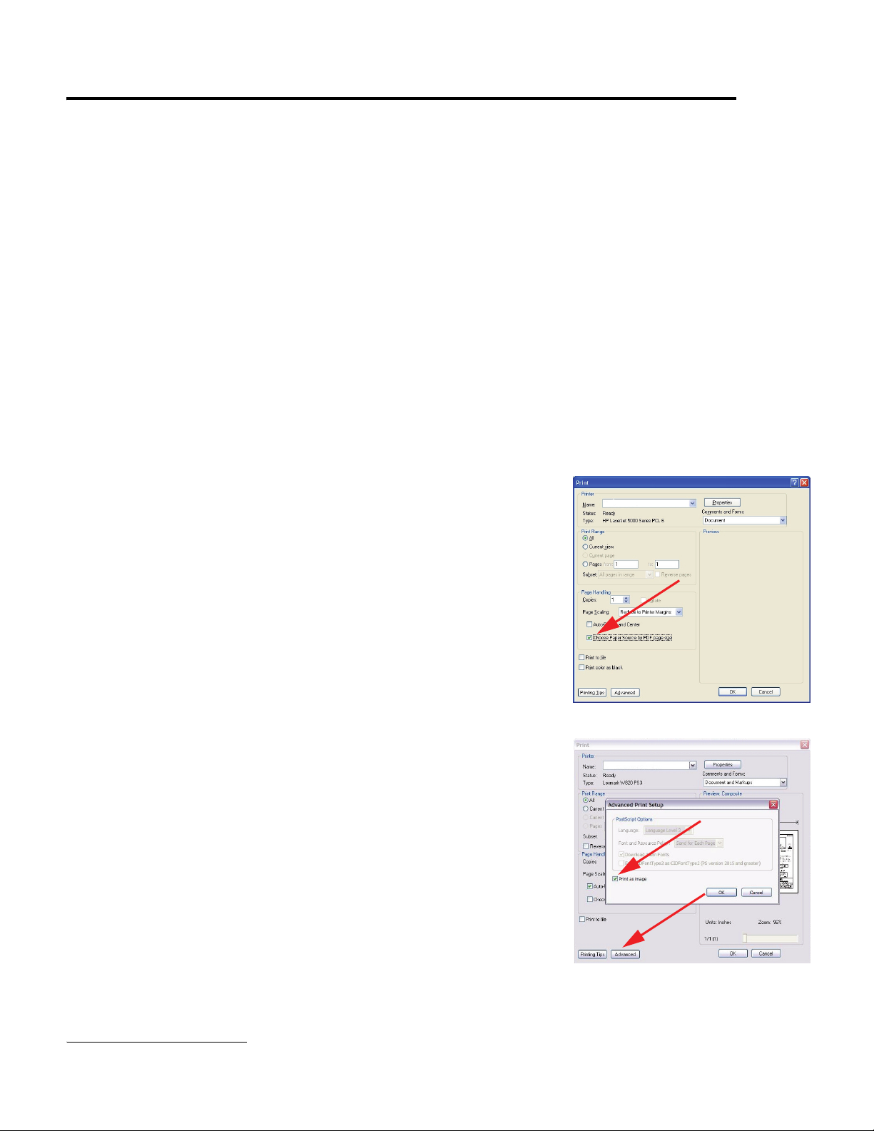
[1] PRINTING FROM THIS BOOK
1
[1.1] Automatically Print Oversized Pages
When you print this manual from Adobe® Acrobat®, the book will automatically print to
the (default) page size. If you want the oversized sized pages to automatically print to a
larger page size, do the following:
1. In Adobe Acrobat, select File > Print.
2. In the Print dialog box, in the Page Handling section, select Chose Paper
Source by PDF page size.
3. Select OK to print.
[1.2] Printing Complicated Graphics
This book contains a large number of complicated graphics. Depending on your printer,
you may have difficulties printing some of these graphics. To correct this problem, do the
following:
1. In Adobe Acrobat, select File > Print.
2. In the Print dialog box, select Advanced.
3. In the Advanced Print Setup dialog box, select Print as Image.
4. Select OK to print.
1. These instructions may differ slightly depending on what version and type of Adobe Acrobat yo u are using.
i
Page 3
LC-32WD1E/S/RU and LC-32WT1E
[2] SAFETY PRECAUTIONS
IMPORTANT SERVICE SAFETY PRECAUTION
Service work should be performed only by qualified service technicians who are thoroughly familiar with all safety checks and the
servicing guidelines which follow:
WARNING
1. For continued safety, no modification of any circuit should be
attempted.
2. Disconnect AC power before servicing.
CAUTION:
FOR CONTINUED PROTECTION AGAINST A
RISK OF FIRE REPLACE ONLY WITH SAME
TYPE FUSE.
BEFORE RETURNING THE RECEIVER
(Fire & Shock Hazard)
Before returning the receiver to the user, perform the following
safety checks:
3. Inspect all lead dress to make certain that leads are not pinched,
and check that hardware is not lodged between the chassis and
other metal parts in the receiver.
4. Inspect all protective devices such as non-metallic control knobs,
insulation materials, cabinet backs, adjustment and compartment
covers or shields, isolation resistor-capacitor networks, mechanical
insulators, etc.
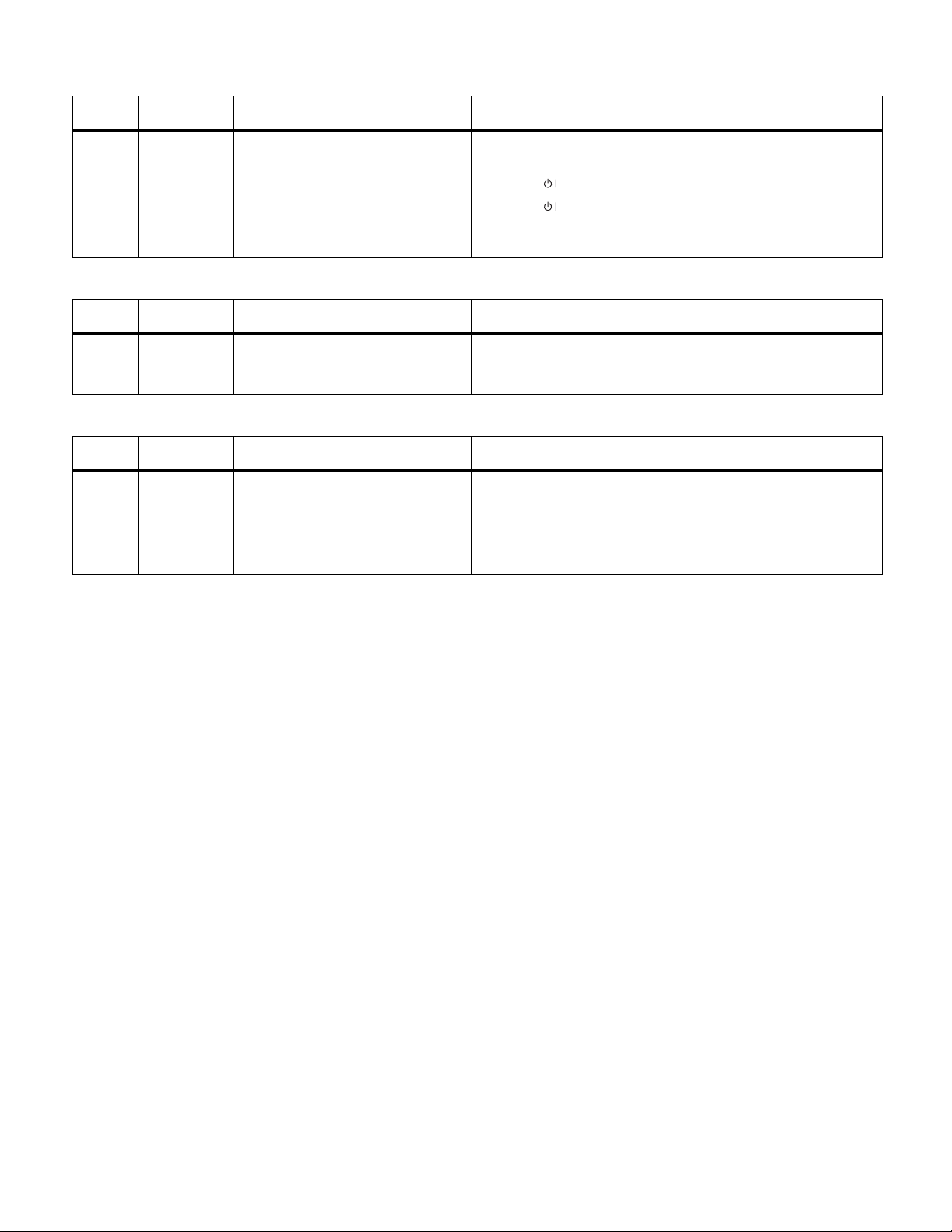
5. To be sure that no shock hazard exists, check for leakage current in
the following manner.
• Plug the AC cord directly into a 220~240 volt AC outlet.
• Using two clip leads, connect a 1.5k ohm, 10 watt resistor paralleled by a 0.15μF capacitor in series with all exposed metal cabinet
parts and a known earth ground, such as electrical conduit or electrical ground connected to an earth ground.
///////////////////////////////////////////////////////////////////////////////////////////////////////////////////////////////////////////////////////////////////////////////////////////////////////////////////////////////////////////
• Use an AC voltmeter having with 5000 ohm per volt, or higher, sensitivity or measure the AC voltage drop across the resistor.
• Connect the resistor connection to all exposed metal parts having a
return to the chassis (antenna, metal cabinet, screw heads, knobs
and control shafts, escutcheon, etc.) and measure the AC voltage
drop across the resistor.
All checks must be repeated with the AC cord plug connection
reversed. (If necessary, a nonpolarized adaptor plug must be used
only for the purpose of completing these checks.)
Any reading of 1.05 V peak (this corresponds to 0.7 mA peak AC.)
or more is excessive and indicates a potential shock hazard which
must be corrected before returning the monitor to the owner.
DVM
AC SCALE
1.5k ohm
10W
0.15µF
TEST PROBE
TO EXPOSED
METAL PARTS
CONNECT TO
KNOWN EARTH
GROUND
SAFETY NOTICE
Many electrical and mechanical parts in LCD color television have
special safety-related characteristics.
These characteristics are often not evident from visual inspection, nor
can protection afforded by them be necessarily increased by using
replacement components rated for higher voltage, wattage, etc.
Replacement parts which have these special safety characteristics are
identified in this manual; electrical components having such features
are identified by “ ” and shaded areas in the Replacement Parts
List and Schematic Diagrams.
///////////////////////////////////////////////////////////////////////////////////////////////////////////////////////////////////////////////////////////////////////////////////////////////////////////////////////////////////////////
For continued protection, replacement parts must be identical to those
used in the original circuit.
The use of a substitute replacement parts which do not have the same
safety characteristics as the factory recommended replacement parts
shown in this service manual, may create shock, fire or other hazards.
ii
Page 4
LC-32WD1E/S/RU and LC-32WT1E
r
[3] PRECAUTIONS FOR LEAD-FREE SOLDER
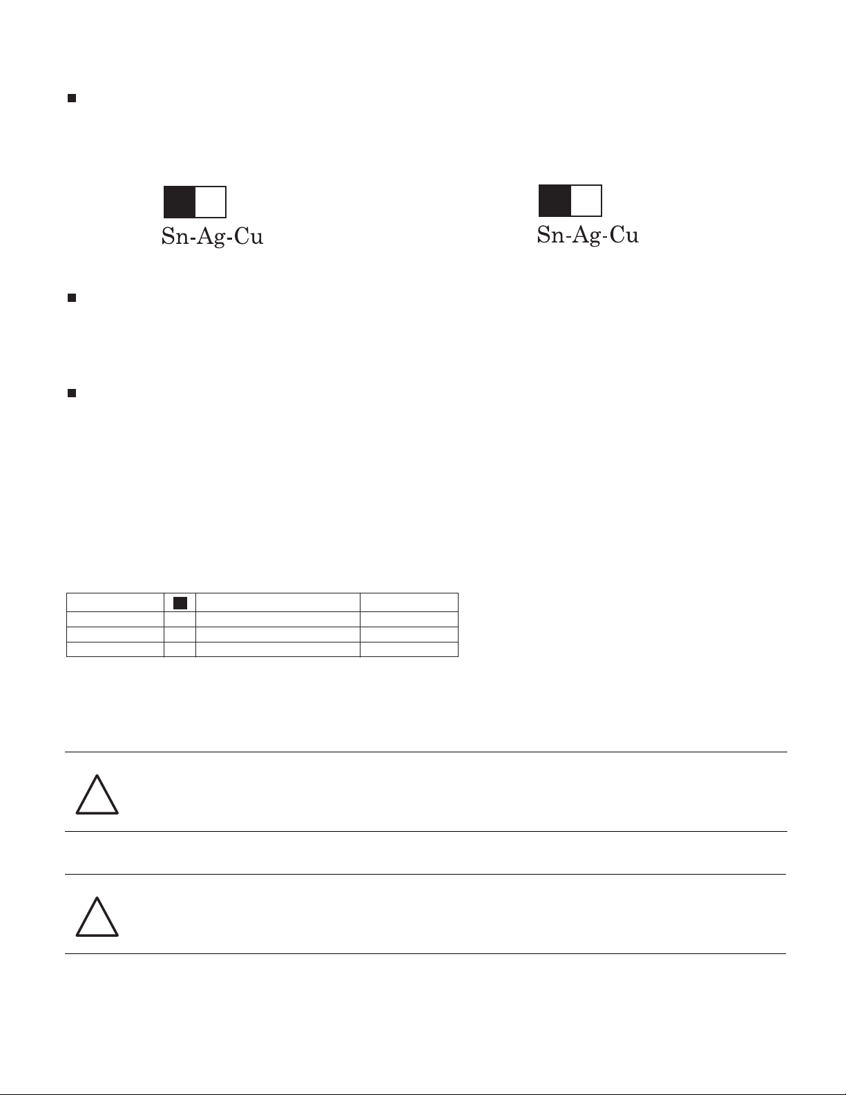
Employing lead-free solder
• “PWBs” of this model employs lead-free solder. The LF symbol indicates lead-free solder, and is attached on the PWBs and service manuals. The
alphabetical character following LF shows the type of lead-free solder.
Example:
L Fa
Indicates lead-free solder of tin, silver and copper.
Using lead-free wire solder
• When fixing the PWB soldered with the lead-free solder, apply lead-free wire solder. Repairing with conventional lead wire solder may cause damage or accident due to cracks.
As the melting point of lead-free solder (Sn-Ag-Cu) is higher than the lead wire solder by 40 °C, we recommend you to use a dedicated soldering
bit, if you are not familiar with how to obtain lead-free wire solder or soldering bit, contact our service station or service branch in your area.
Soldering
• As the melting point of lead-free solder (Sn-Ag-Cu) is about 220 °C which is higher than the conventional lead solder by 40 °C, and as it has poo
solder wettability, you may be apt to keep the soldering bit in contact with the PWB for extended period of time. However, Since the land may be
peeled off or the maximum heat-resistance temperature of parts may be exceeded, remove the bit from the PWB as soon as you confirm the
steady soldering condition.
Lead-free solder contains more tin, and the end of the soldering bit may be easily corroded. Make sure to turn on and off the power of the bit as
required.
If a different type of solder stays on the tip of the soldering bit, it is alloyed with lead-free solder. Clean the bit after every use of it.
When the tip of the soldering bit is blackened during use, file it with steel wool or fine sandpaper.
• Be careful when replacing parts with polarity indication on the PWB silk.
Lead-free wire solder for servicing
edoCnoitpircseD.oN traP
ZHNDAi123250E J φ0.3mm 250g (1roll) BL
ZHNDAi126500E J φ0.6mm 500g (1roll) BK
ZHNDAi12801KE J φ1.0mm 1kg (1roll) BM
Indicates lead-free solder of tin, silver and copper.
L F a/a
[4] SAFETY WARNINGS
[4.1] Service by Qualified Personnel Only
WARNING! THIS MANUAL IS FOR USE BY QUALIFIED SERVICE PERSONNEL ONLY. ALL SERVICING SHOULD BE
REFERRED TO QUALIFIED SERVICE PERSONNEL. TO PREVENT INJURY, UNDER NO CIRCUMSTANCES
!
[4.2] Power Safety
WARNING! BEFORE PERFORMING ANY TYPE OF SERVICE OR REPAIR ON ANY TELEVISION, TURN THE UNIT OFF
SHOULD ANYONE OTHER THAN QUALIFIED SERVICE PERSONNEL ATTEMPT TO REMOVE THE COVER
OF ANY TELEVISION OR SERVICE IT.
AND DISCONNECT ITS AC POWER CORD FROM THE POWER SOURCE.
!
iii
Page 5
LC-32WD1E/S/RU and LC-32WT1E
CHAPTER 1. SPECIFICATIONS
[1] SPECIFICATIONS
Specifications
32” LCD Colour TV
LCD screen size 32” diagonal 37” diagonal 42” diagonal
Number of pixels 1366 x 768
Video colour system PAL, PAL 60, NTSC 3.58, NTSC 4.43, SECAM
Sound standard B/G, L/L’, I, D/K
TV
Function
Brightness
Backlight life 60,000 hours
Viewing Angles H: 176° V: 176°
Audio amplifier Class D audio amplifier, 2x 10Watt
Speaker 126 mm x 58 mm
Terminals Rear Antenna UHF/VHF 75 ohm Din type (Analogue & Digital)
OSD Languages English, German, French, Spanish, Dutch, Portuguese, Turkish, Greek, Russian,
Power Requirement AC 220-240 V, 50 Hz
Power Consumption 141 W
Weight 19 kg (display with stand)
Operating Temperature 0°C – 35°C
a. Model numbers: LC-32WD1E, LC-32WT1E, LC-32WD1S, LC-32WD1RU
b. Model numbers: LC-37WD1E, LC-37WT1E, LC-37WD1S, LC-37WD1RU
c. Model numbers: LC-42WD1E, LC-42WT1E, LC-42WD1S, LC-42WD1RU
TV-Standard Analogue CCIR (B/G, I, D/K, L, L’)
Digital DVB-T (2K/8K OFDM)
Receiving
Channels
TV Tuning System Auto Preset channels, Auto Label, Auto Sort
Stereo/Bilingual NICAM/A2
Side EXT 3 S-Video (Y/C input), CVBS input, left/right RCA pin audio input
VHF/UHF E2-E69ch, F2-F10ch, I21-I69ch, IR A-IR Jch, (Digital: E5-E69ch)
CATV Hyper-band, S1-S41ch
450 cd/m
EXT 1 SCART (S-Video input, analogue RGB input, CVBS input, tuner CVBS output)
EXT 2 SCART (S-Video input, analogue RGB input, CVBS input/output)
EXT 4 Component Video input (Y,P
EXT 5
EXT 6
EXT 7 HDMI input
CI-Slot
(Common
Interface)
Output Left/right RCA pin audio output
Service D-Sub 9 Service port (for qualified service personnel only)
Headphones
VGA input, 3.5 mm stereo input
HDMI input, 3.5 mm stereo input
EN50221, R206001
∅
Italian, Polish, Swedish, Finnish
(<9 W Active standby)
(<1 W Passive standby)
17 kg (display only)
2
3.5 mm jack (audio output)
a
∅
∅
37” LCD Colour TV
B,PR input), left/right RCA pin audio input
177 W
(<9 W Active standby)
(<1 W Passive standby)
25 kg (display with stand)
21.5 kg (display only)
b
42” LCD Colour TV
190 W
(<9 W Active standby)
(<1 W Passive standby)
30 kg (display with stand)
26.5 kg (display only)
c
As a part of policy of continuous improvement, SHARP reserves the right to make design and specification changes for product
improvement without prior notice. The performance specification figures indicated are nominal values of production units. There may
be some deviations from these values in individual units.
1 - 1
Page 6
LC-32WD1E/S/RU and LC-32WT1E
CHAPTER 2. OPERATION MANUAL
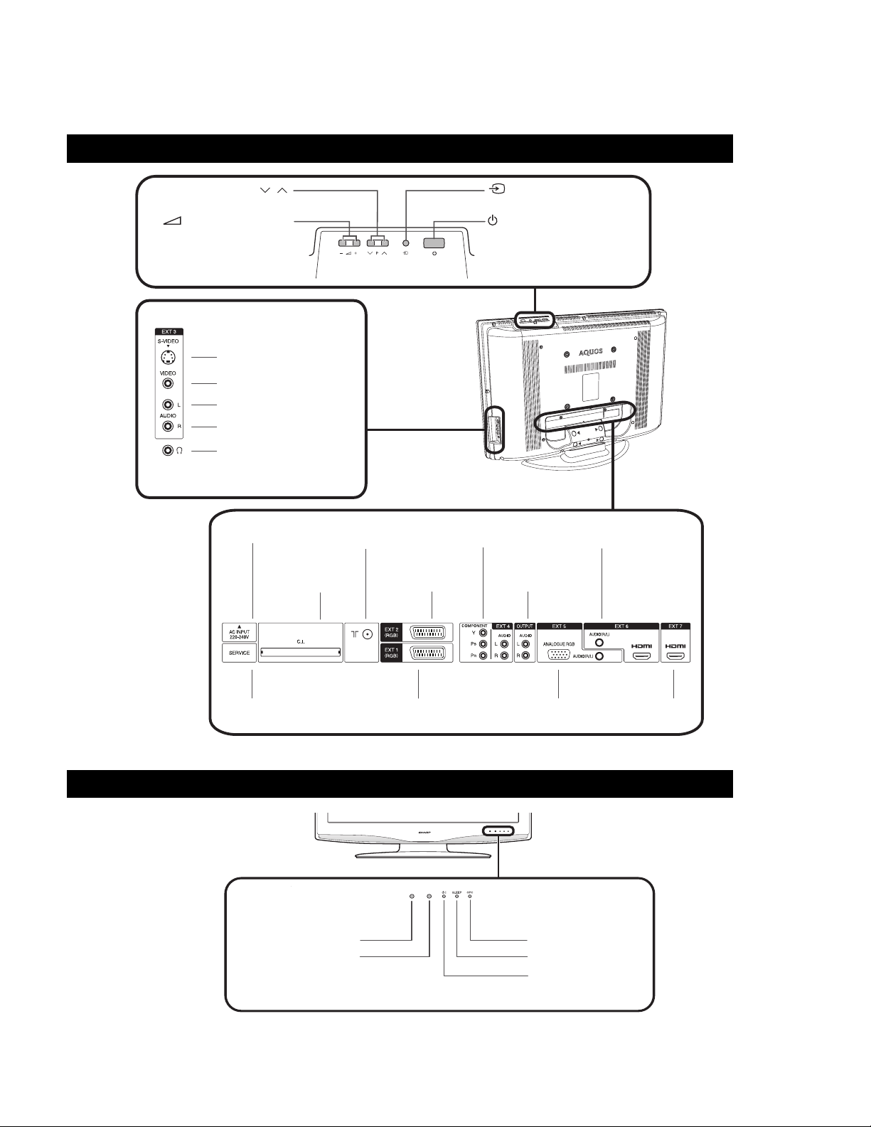
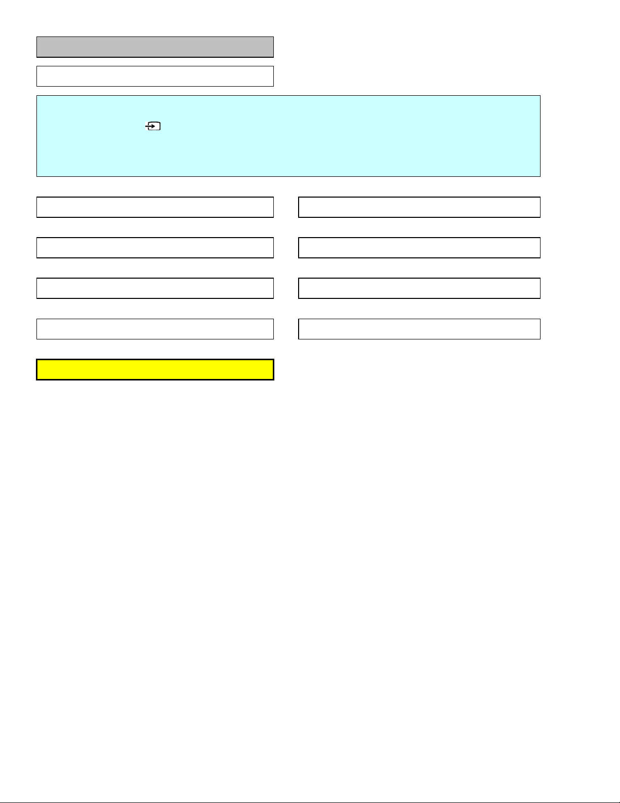
[1] OPERATION MANUAL
Television rear and side view
P (
)
(Programme [channel] buttons)
(- / + ) (Volume buttons)
EXT 3 Connections
S-Video input (Y/C)
Composite input (CVBS)
Audio input - Left
Audio input - Right
Headphones (audio out)
The S-Video (Y/C) and composite (CVBS) connection
cannot be used at the same time.
/
AC Input
Common
Interface slot
Antenna input
(DVB-T 5V=/80 mA)
EXT 2
(SCART input/output)
(Input button)
(Standby/On button)
EXT 4
(Component input)
Audio output
EXT 6 (HDMI input, Stereo input
for DVI-HDMI connections)
TV front view
Service (D-Sub 9)
Remote control sensor
OPC sensor
EXT 1*
(SCART input/output)
2 - 1
EXT 5 (VGA / Stereo input)
*EXT 1 provides tuner output. Use EXT 1 to connect a decoder or
audiovisual equipment used for recording purposes (ex. VCR).
OPC LED indicator
SLEEP LED indicator
Standby/On LED indicator
Remote Control
indicator
EXT 7
(HDMI input)
Page 7
LC-32WD1E/S/RU and LC-32WT1E
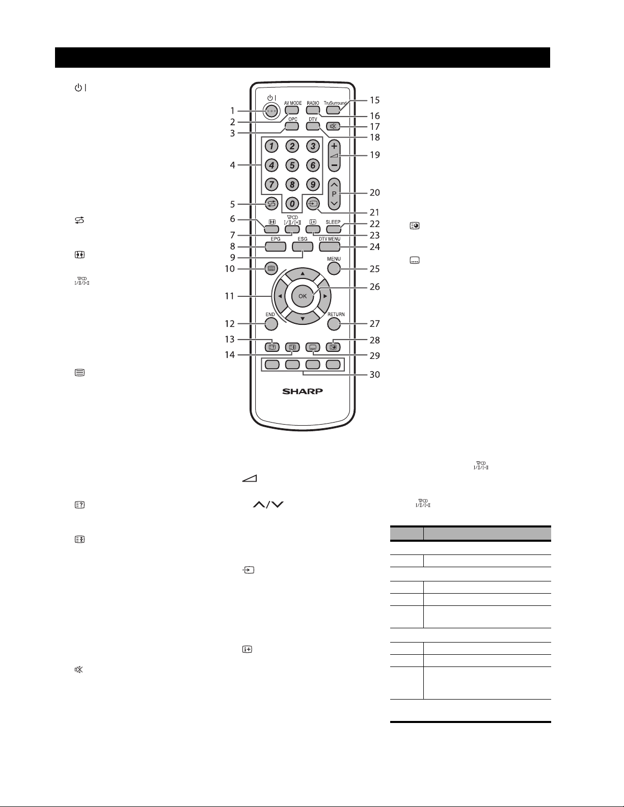
Remote control function
1
2AV MODE
3OPC
4 0–9
5
6
7
8EPG
9ESG
10
11 S/T/W/X (Cursor)
12 END
13
14
15 TruSurround
16 RADIO
17
(Standby/On)
Switches the TV between on and
standby mode.
Selects a preset audio/video setting
(AV Mode).
Turns the Optical Picture Control
(OPC) “On” and “Off”.
TV/DTV: Directly selects the channel.
Teletext: Selects the page.
(Flashback)
Returns to the previous channel or AV
input.
(WIDE MODE)
Selects wide mode.
(Sound mode)
See “Using Multiplex” on page 2.
DTV: Displays the EPG (Electronic
Programme Guide) screen.
DTV: Displays the ESG (Electronic
Service Guide) screen.
(Teletext)
TV: Selects the teletext mode. (See
page 21.)
DTV: Selects the teletext mode or
MHEG5 (if available). If both are
available, press for MHEG5. Press for
1-2 seconds for teletext.
Selects an item on the screen.
Press to exit the on-screen display
menu screen.
(Reveal hidden teletext)
Reveals/hides hidden teletext
information.
(Freeze/Hold)
TV/DTV/External: Freezes the onscreen image.
Teletext: Stop updating teletext pages
automatically or release the hold
mode.
Turns SRS TruSurround® “On” and
“Off”.
DTV: Switches between RADIO and
DTV Mode.
(Mute)
Turns the sound “On” and “Off”.
18 DTV
Switches between analogue TV mode
and DTV mode.
19
20
21
22 SLEEP
23
(+ / -) (Volume)
Increases or decreases the volume.
P ()
TV/DTV: Selects the channel.
External: Switches to TV or DTV input
mode.
Teletext: Move to the next or previous
page.
(Input source)
Selects an input source.
Sets the amount of time the TV will
stay on before automatically turning
off. (In units of 30 minutes to a
maximum of 2 hours 30 minutes.)
(Display information)
TV: Displays channel information. (See
page 21.)
DTV: Displays the service banner.
24 DTV MENU
DTV: Displays the DTV on-screen
display menus.
25 MENU
Displays the Main TV on-screen
display menus.
26 OK
Selects an option in the on-screen
display menu. Displays the programme
list (except for external input).
27 RETURN
Returns to the previous menu.
28
(Subpage)
Displays current time.
Teletext: Displays or hides subpages.
29
(Subtitle for Teletext)
TV/External: Turns the teletext
subtitles “On” and “Off”.
DTV: Displays/hides the subtitle
selection.
30 Colour (Red/Green/Yellow/Blue)
TeleText: Selects a group or block of
pages displayed in the coloured
brackets at the bottom of the screen by
pressing the corresponding colour
button on the remote control.
DTV: When using the on-screen
display, assigned tasks as indicated at
the bottom of the screen.
Using Multiplex
DTV mode— Press to change
languages.
Analogue TV mode—Each time you
press , the mode switches as
illustrated in the following table.
Signal Selectable Item
Mono
Mono Mono
A2 TV broadcasts selection
Mono Mono
Stereo Stereo, Mono
Dual Channel A (I), Channel B (II),
Channel AB (I+II)
NICAM TV broadcasts selection
Mono NICAM Mono
Stereo NICAM Stereo, FM/AM* Mono
Dual NICAM Channel A (I), NICAM
Channel B (II), NICAM Channel
AB (I+II), FM/AM Mono*
* Depending on the country, the option is
either AM or FM mono.
Page 8
LC-32WD1E/S/RU and LC-32WT1E
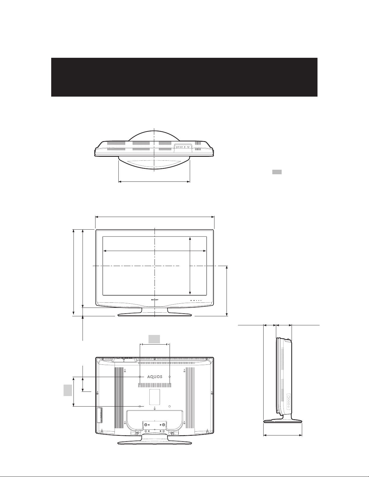
CHAPTER 3. DIMENSIONS
[1] DIMENSIONS
LC-32WD1E / LC-37WD1E / LC-42WD1E
LC-32WT1E / LC-37WT1E / LC-42WT1E
LC-32WD1S / LC-37WD1S / LC-42WD1S
LC-32WD1RU / LC-37WD1RU / LC-42WD1RU
(499.3) / [547.1] / ((547.1))
(499,3) / [547,1] / ((547,1))
(796.0) / [913.0] / ((1027.0))
(796,0) / [913,0] / ((1027,0))
(700.0) / [822.6] / ((933.0))
(700,0) / [822,6] / ((933,0))
( ) : LC-32WD1E
LC-32WT1E
LC-32WD1S
LC-32WD1RU
[ ] : LC-37WD1E
LC-37WT1E
LC-37WD1S
LC-37WD1RU
(( )) : LC-42WD1E
LC-42WT1E
LC-42WD1S
LC-42ED1RU
:
LC-32WD1E
LC-32WT1E
LC-32WD1S
LC-32WD1RU
LC-37WD1E
LC-37WT1E
LC-37WD1S
LC-37WD1RU
LC-42WD1E
LC-42WT1E
LC-42WD1S
LC-42WD1RU
(530.5) / [598.2] / ((673.0))
(530,5) / [598,2] / ((673,0))
(587.6) / [655.3] / ((730.0))
(587,6) / [655,3] / ((730,0))
((57.1))
((57,1))
(57.1) / [57.1]
(57,1) / [57,1]
((45.6))
((45,6))
(114.2) / [87.2]
(114,2) / [87,2]
200.0
200,0
200.0
200,0
(394.6) / [463.8] / ((526.0))
(394,6) / [463,8] / ((526,0))
3 - 1
(341.8) / [376.0] / ((418.0))
(341,8) / [376,0] / ((418,0))
(82.1) / [116.1]
(82,1) / [116,1]
((115.3))
((115,3))
(243.0) / [293.0]
(243,0) / [293,0]
((293.0))
((293,0))
(110.0) / [110.0]
(110,0) / [110,0]
((111.0))
((111,0))
Page 9
LC-32WD1E/S/RU and LC-32WT1E
CHAPTER 4. REMOVING OF MAJOR PARTS
[1] REMOVE MAJOR PARTS LC-32WD1E/S/RU AND LC-32WT1E/S
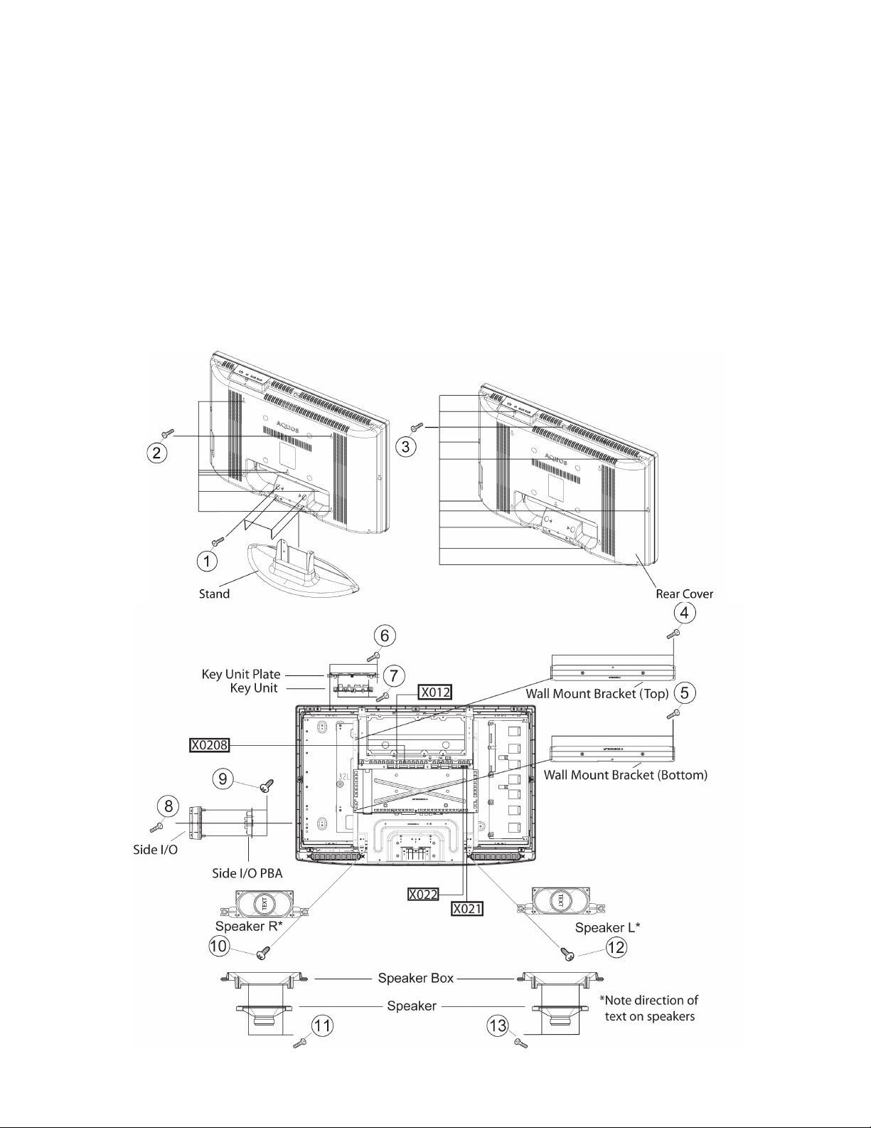
1. Remove the 4 lock screws (1). Detach the Stand.
2. Remove the 7 lock screws (2). Remove the 10 lock screws (3). Detach the Rear Cover.
3. Remove 4 lock screws (4). Detach Wall Mount Bracket (Top).
4. Remove 4 lock screws (5). Detach Wall Mount Bracket (Bottom).
5. Disconnect cable (X012). Remove 2 lock screws (6) and detach Key Unit Plate.
6. Remove 2 lock screws (7) and detach Key Unit.
7. Disconnect cable (X0208). Remove 1 lock screw (8). Detach Side I/O.
8. Remove 2 lock screw (9). Detach Side I/O PBA.
9. Disconnect cable (X021). Remove 1 lock screws (10). Detach Speaker R.
10. Remove 4 lock screws (11). Detach Speaker from Speaker Box.
11. Disconnect cable (X022). Remove 1 lock screw (12). Detach Speaker L.
12. Remove 4 lock screws (13). Detach Speaker from Speaker Box.
4 - 1
Page 10
LC-32WD1E/S/RU and LC-32WT1E
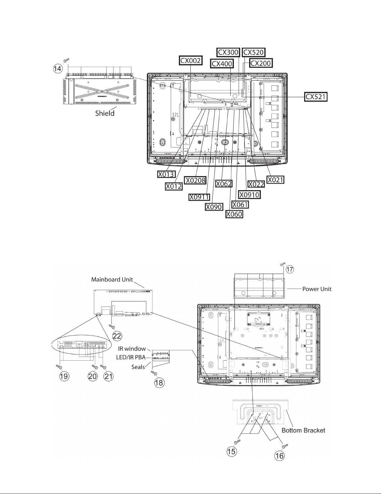
13. Remove all the connections from PWBs.
14. Remove 6 lock screws (14). Dismount power cable. Remove Shield.
15. Remove 3 lock screws (15). Remove 2 lock screws (16). Detach Bottom Bracket.
16. Remove 9 lock screws (17). Deta ch Power Unit.
17. Remove 2 lock screws (18). Detach IR/LED PBA, IR Window, and Seals.
18. Remove 4 lock screws (19). Remove 4 lock screws (20). Remove 2 lock screws (21).
19. Remove 2 lock screws (22). Deta ch Mainbo ard Unit.
4 - 2
Page 11
LC-32WD1E/S/RU and LC-32WT1E
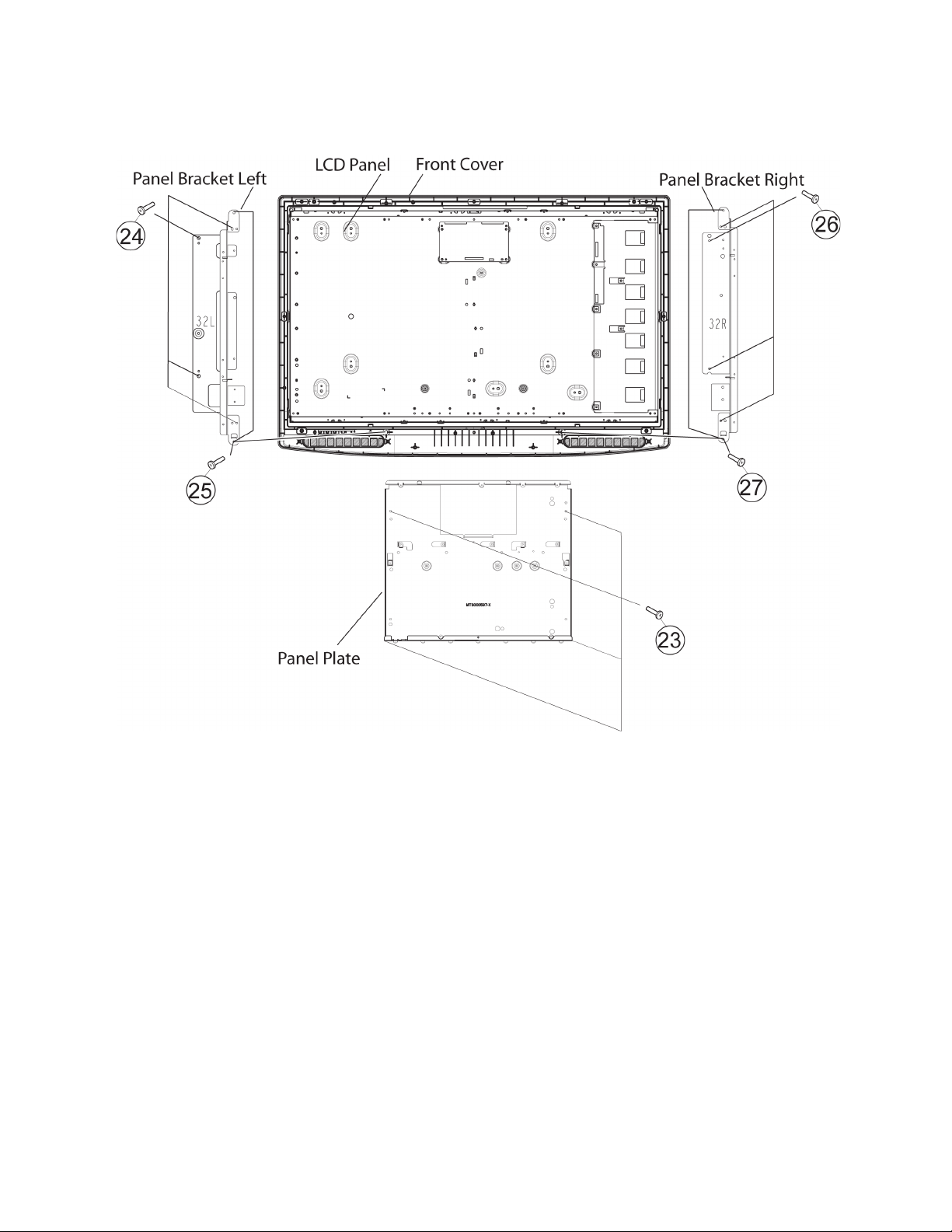
20. Remove 4 lock screws (23). Remove Panel Plate.
21. Remove 4 lock screws (24). Remove 2 lock screws (25). Remove Panel Bracket Left.
22. Remove 4 lock screws (26). Remove 2 lock screws (27). Remove Panel Bracket Right.
23. Remove the LCD panel from the Front Cover.
4 - 3
Page 12
LC-32WD1E/S/RU and LC-32WT1E
CHAPTER 5. ADJUSTMENT PROCEDURES
[1] UPGRADING SOFTWARE
[1.1] File types and Hardware/Software Requirements
File Type Hardware Software
All Upgrades • Controlling PC
(running Microsoft® Windows®)
• Television
• Power cable
• Remote control
Analogue • UOC/GTV application
(.hex)
• PNX application(s) (.mi)
• PNX config files (.cfg)
• PNX EEPROM (.eeprom)
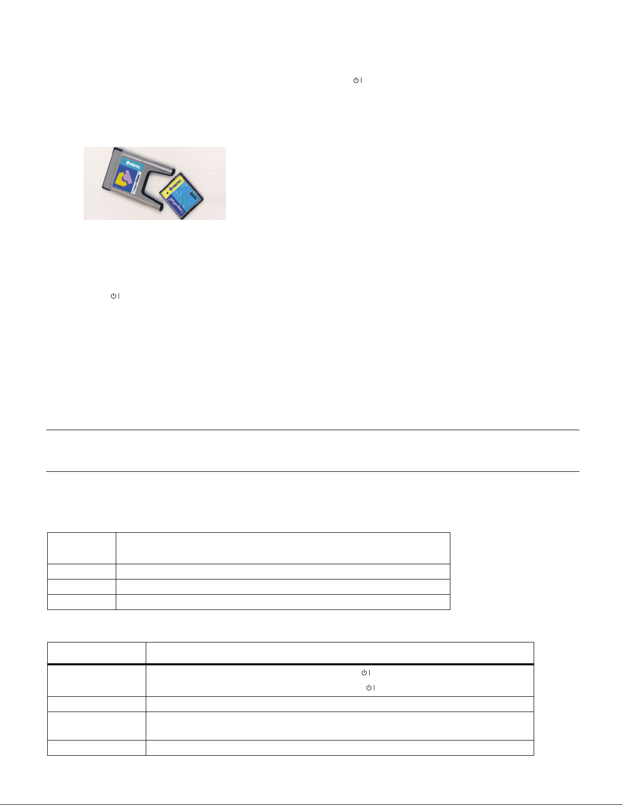
Digital • ST/Futarque DTV (.bin) • PCMCIA Comp act Flash (CF)
UOC eeprom • This software should never be upgraded. This device is written (initialized) automatically during the installa-
tion procedure at first power-on.
• Service PCB
• Jumper
• Telos “Connii MM” I2C/USB
device
• PS2 MiniDIN Cable
• USB cable (up/down stream)
adapter
• CF mem ory card
• Latest software package and
release notes
• ServUpdtTelos_v1_8.exe
Application for controlling the
update
• FlashFlame 4.1.exe
UOC chip driver for Windows
• telos_multimaster_setup-2_0.exe
Drivers for the controlling PC
• Microsoft .NET Framework 1.1
(Download from Internet)
[1.2] T ime Requirements
Image Time required
Analogue +/- 8 minutes
/gtv_flash.hex +/- 40 seconds
/bffs0/app.mi +/- 440 seconds
/bffs0/dsw.mi +/- 150 seconds
/bffs0/gamma.cfg +/- 4 seconds
/bffs0/hdcp.cfg +/- 4 seconds
/bffs0/profile.cfg +/- 4 seconds
/PNX Eeprom +/- 10 seconds
Digital +/- 120 seconds
Data 6 seconds
HDMI-A EDID +/- 2 seconds
HDMI-D EDID +/- 2 seconds
VGA EDID +/- 2 seconds
5 - 1
Page 13
LC-32WD1E/S/RU and LC-32WT1E
[1.3] Analogue Upgrade
[1.3.1] Analogue Upgrade Software Setup
Refer to “File types and Hardware/Software Requirements” on page 5-1.
1. Install telos_multimaster_setup-2_0.exe.
2. Install FlashFlame 4.1.exe.
3. If necessary, download and install Microsoft .NET Framework 1.1. (This is typically included in most Windows installations.)
4. To verify the installation is correct, open ServUpdtTelos_v1_8.exe. The application should open with no errors. Close the
application.
[1.3.2] Analogue Upgrade Hardware Setup
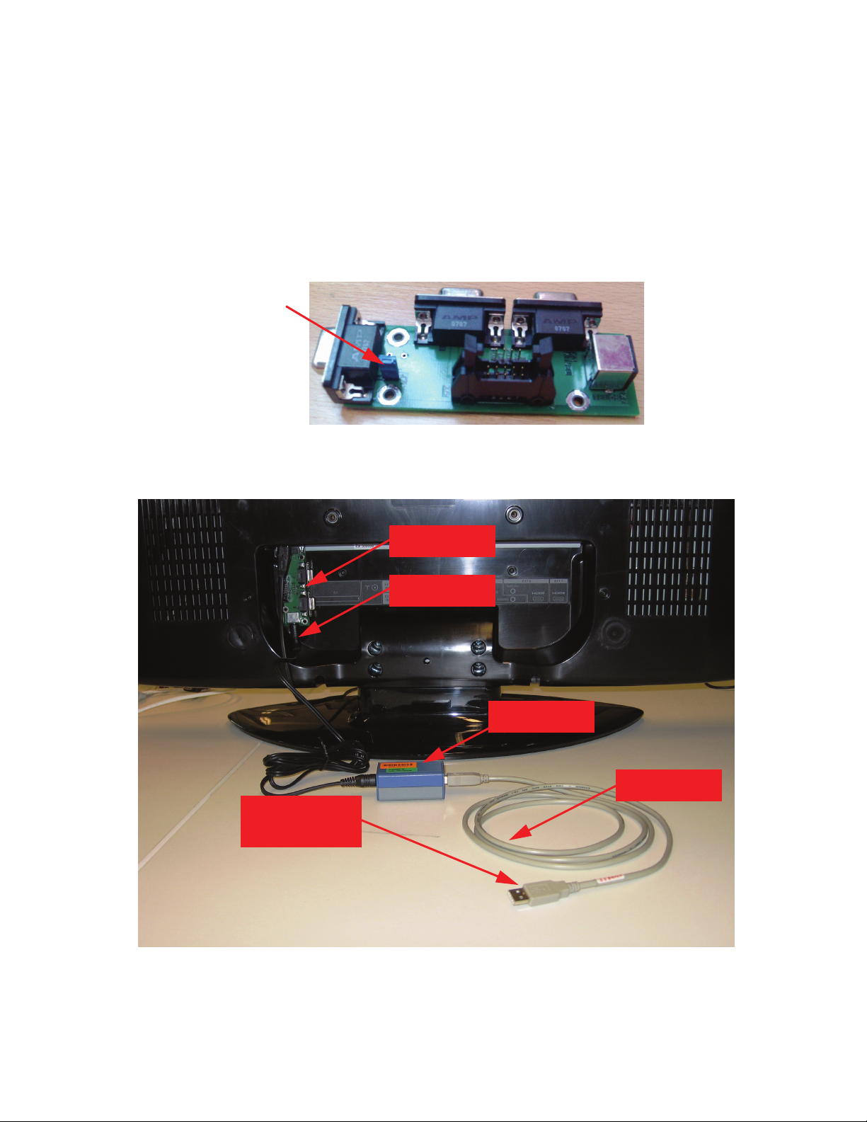
1. On the Service PCB, install the jumper to shortcut the X2 jumper position.
Jumper
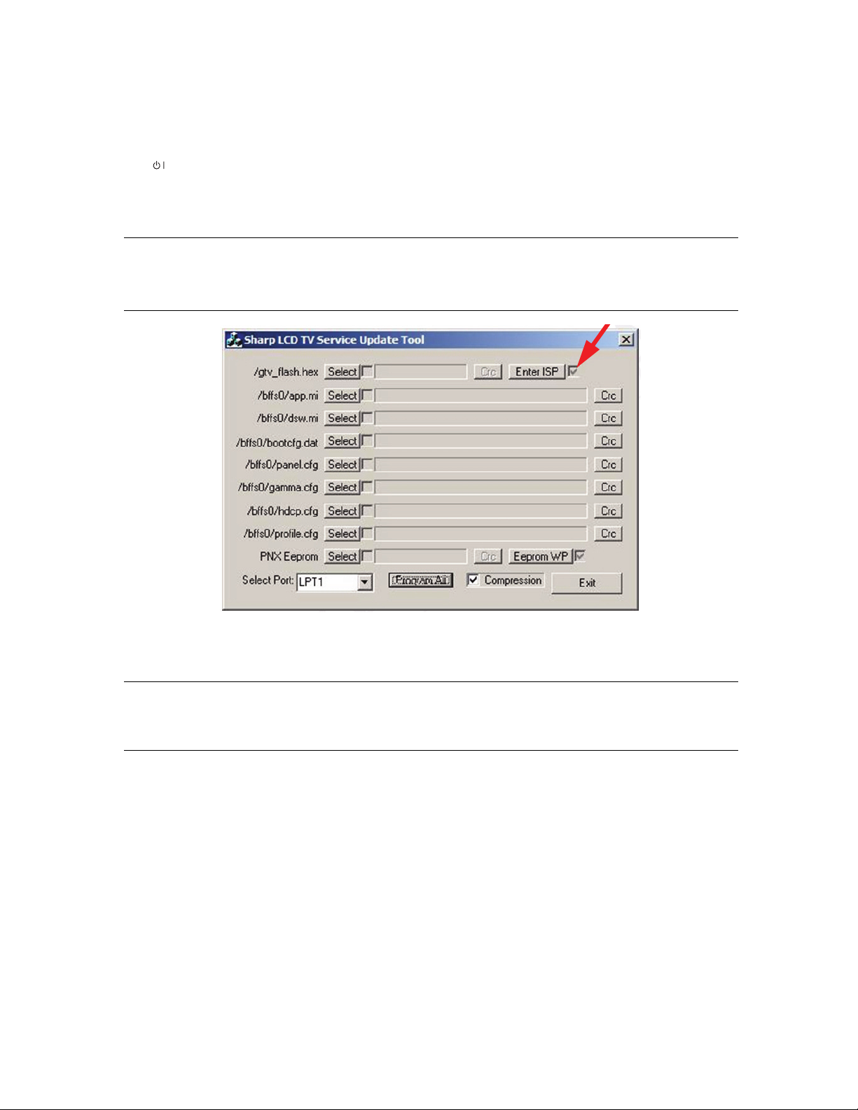
2. Connect the Service PCB to the TV by the DB9 connector. (Refer to “Television rear and side view” on page 2-1.)
3. Connect the MiniDIN cable to the Service PCB. Connect the other end of the MiniDIN cable to the Telos device.
4. Connect the USB cable to the T elos device. (Do not connect the other end of the USB cable to the TV at this time.)
To controlling PC
(later step)
Service PCB
MiniDIN cable
Telos device
USB cable
5 - 2
Page 14
LC-32WD1E/S/RU and LC-32WT1E
[1.4] Analogue Upgrade Process
1. Disconnect the TV from AC power. Wait 10 seconds.
Do NOT go to standby first. Just unplug the power cord.
2. Connect the TV with the set up as described in “Analogue Upgrade Hardware Setup” on page 5-2.
3. Connect the TV to AC power.
4. Press to turn the TV on. (The Standby/On LED on the front of the TV is GREEN.)
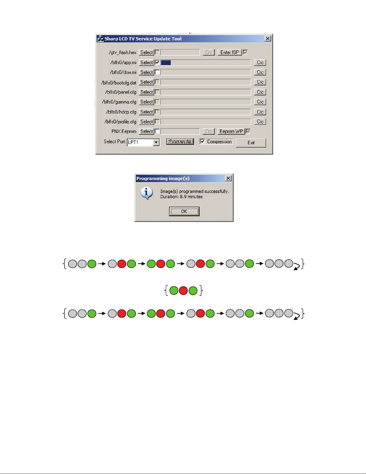
5. Open ServUpdtTelos_v1_8.exe.
6. Connect the USB cable (connected to the Service PCB and Telos device assembly) to the controlling PC.
7. In ServUpdtTelos_v1_8.exe, be sure that the checkbox by Enter ISP is highlighted automatically.
Note:
8. Select the image file(s) you want to upgrade.
a. For each image file that you want to upgrade, press Select to open a browse window.
b. Browse to the location of the new image files and select the file.
If Enter ISP is not automatically checked, try to select the Enter ISP button. If this does
not highlight the checkbox, close the application and re-check your setup as described in
“Analogue Upgrade Hardware Setup”, power the TV on and off, and then start over at
step1.
Note:
• The image files must be on the hard drive of the controlling PC. They cannot be on a
network connection.
• The image file names may vary. Use the release notes to identify the correct image
file.
5 - 3
Page 15
LC-32WD1E/S/RU and LC-32WT1E
c. Select Program All to start the upgrade. DO NOT INTERRUPT THIS SEQUENCE!
9. When finished, a message similar to this will be displayed:
10. Close your PC application.
11. If you updated the GTV image (.hex file), it is possible the LEDs on the front of the TV will blink and illuminate for
approximately 30 seconds. This is the virgin TV Init process. Wait until the LEDs are off, and then the TV will start up
automatically.
Step 1: Visual notification for the start of the EEPROM TV initialization (3 sequences)
Step 2: Visual notification for the TV initialization / data writing (1 sequence):
Step 3: Visual notification for the end of the eeprom TV initialization (3 sequences)
12. Disconnect the Service PCB from the TV.
13. Disconnect the TV from AC power. Wait 10 seconds.
14. Connect the TV to AC power. The TV will turn on automatically. (Standby/On LED is GREEN.)
15. Verify the TV was upgraded correctly. (See “Service Menu Settings” on page 7.)
5 - 4
Page 16
LC-32WD1E/S/RU and LC-32WT1E
[1.5] Digital Upgrade Process
1. Place the latest digital software on the CF card. (Refer to the release notes to identify the correct file.)
2. If the TV is not already on, connect the TV to AC power and press to turn the TV on.
3. Press DTV on the remote control to put the television into DTV mode.
4. Disconnect the TV from AC power. Wait 10 seconds.
Do NOT go to standby first. Just unplug the power cord.
5. Insert the CF card into the PCMCIA CF adapter.
6. Insert the PCMCIA CF adapter into the CI-slot on the rear panel of the TV. (Refer to “Television rear and side view” on
page 2-1.)
7. Connect the TV to AC power.
The upgrade process will start. The message “Digital TV, Starting” will display on the screen.
8. When the “Digital TV, Starting” message is no longer on the TV, the upgrade process is complete.
9. Press to turn on the TV.
10. Using the remote control, verify that the TV was upgraded correctly by going to the following screen:
Press DTV and then press DTV MENU. Go to Installation > About.
[2] ENTERING THE PUBLIC MODE MENUS
1. On the remote control, press MENU.
•The TV Menu screen displays.
2. Enter the PIN code “3001”.
• Using the number keypad, press 3, then 0, then 0, and then 1. (Each button in the sequence must be pressed
immediately after the button before it or the television will not recognize the entry code.)
Note:
Depending on the Public Mode settings, the TV Menu screen may not be visible when Public Mode is
activated. To open the Public Mode me nu, the user still needs to open the TV Menu (which remains hidden)
and enter “3001”.
[3] REMOTE CONTROL KEY OPERATION IN PUBLIC MODE
[3.1] Remote Control Key Operation
Remote
Control Key Function / Remark
S/T
W/X
END Press to exit the service menus.
Press to move up and down and select the desired item.
Press to change the setting of the selected item.
[4] PUBLIC MODE SETTINGS
Item Available Settings and Description
Power On Fixed
Maximum Volume [Range] — The volume level specified here is the maximum volume level for the TV.
Volume Fixed Variable — The sound volume is not fixed.
Volume Fixed Level [Range] — The volume level specified here is the fixed volume level for the TV.
Variable — The TV will go into standby mode when is pressed.
Fixed — The TV will not go into standby mode when is pressed.
Fixed — The sound volume is fixed to the level set in “Volume Fixed Level”.
5 - 5
Page 17
LC-32WD1E/S/RU and LC-32WT1E
Item Available Settings and Description
RC Button Respond — The TV will respond when buttons are pressed on the remote control.
No Respond — The TV will not respond when buttons are pressed on the remote control.
Panel Button Respond — The TV will respond when buttons are pressed on the panel / keypad.
No Respond — The TV will not respond when buttons are pressed on the panel / keypad.
Menu Button Respond — The TV will respond when Menu and DTV Menu are pressed.
No Respond — The TV will not respond when Menu and DTV Menu are pressed.
On Screen Display On — The on screen display menus will behave normally.
Off — The on screen display menus will not display.
Input Mode Start [Variable] — When the TV is turned on, the TV will start-up in this input mode.
Input Mode Fixed On — The input mode is fixed to the mode set in “Input Mode Start”.
Off — The input mode is not fixed.
Reset Resets the Public Mode setting s to the factory defaults.
Public Mode On — The TV will follow the settings specified in the Public Mode menu.
Off — The TV will ignore the settings specified in the Public Mode menu.
[5] ENTERING THE SERVICE MENUS
1. On the remote control, press MENU.
•The TV Menu screen displays.
2. Enter the PIN code “1147”.
• Using the number keypad, press 1, then 1, then 4, and then 7. (Each button in the sequence must be pressed
immediately after the button before it or the television will not recognize the entry code.)
[6] SERVICE MODE REMOTE CONTROL KEY AND DESCRIPTION OF DISPLAY
[6.1] Remote Control Key Operation
Remote
Control Key Function / Remark
1 - 9 Enter the item number (3-digit format) to go to the specified item.
S/T
W/X
END Press to exit the service menus.
[6.2] Description of Display
*Where “X” indicates the version of the software package.
Press to scroll one-by-one through the service item screens.
Press to change the setting of the selected service item.
Item Category* Setting
INTROADRUNNERXX
Item #
001
00000000
01000000
11000010
00000000
Init TV 0
00000000
00111100
5 - 6
Page 18
LC-32WD1E/S/RU and LC-32WT1E
[7] SERVICE MENU SETTINGS
CAUTION:
Item # Item
000 GTV
001 Init TV 0 = Off
276 Gam-20IRE-R 0 - 255 White Point Calibration. See “Using White Point Calibration Items” on page 5-8.
277 Gam-80IRE-R 0 - 255 White Point Calibration. See “Using White Point Calibration Items” on page 5-8.
278 Gam-20IRE-G 0 - 255 White Point Calibration. See “Using White Point Calibration Items” on page 5-8.
279 Gam-80IRE-G 0 - 255 White Point Calibration. See “Using White Point Calibration Items” on page 5-8.
280 Gam-20IRE-B 0 - 255 White Point Calibration. See “Using White Point Calibration Items” on page 5-8.
281 Gam-80IRE-B 0 - 255 White Point Calibration. See “Using White Point Calibration Items” on page 5-8.
858 Virgin bit 0 = Off
925 Last Error
926 Error Count Not Applicable Number of times the set went into reset due to an error.
927 LCD Size 1 = LC-32WD1E
Only the items described in this section should be modified. Do not modify any other se tti ngs available in
the service menus.
Available
Settings Remarks (adjustment details, etc.)
Not Applicable 1st line describes the overall SW package version name (See [6.2].)
Application
X = Activate
1 = On
Not Applicable The last error code recorded.
Code
1 = LC-32WT1E
2 = LC-32WD1S
3 = LC-32WD1RU
2nd line describes the UOC/GTV SW version
3rd line on the right describes the PNX SW version
Initialization to factory settings. When the factory settings have been made, all
user setting data, including the channel settings, are initialized. (The
adjustments done in the adjustment process mode are not initialized.)
See “Using Init TV” on page 5-7.
Puts the TV into virgin mode. When the TV is restarted, the TV will start in virgin
mode. The Auto Install menu (wizard) will start when the TV is restarted, but the
EEPROM settings are not erased. See “Using Virgin Bit” on page 5-9.
0x00 = DTV HANGUP
0x01 = POWER_ON_RESET
0x02 = SUPPL Y_V OLTAGE_INDICATION_ERROR
0x04 = OUTPUT_VERTICAL_GUARD_ERROR
0x08 = XRAY_PROTECTION_ERROR
0x10 = PROTECTION_1_8V_SUPPLY_VOLTAGE_ERROR
Sets the panel size of the TV . Set this setting after replacing the mainboard. This
setting must be set to make sure the right settings are loaded for this TV
(gamma table, etc.).
[7.1] Using Init TV
CAUTION:
Item # Item Adjustment Conditions Adjustment Procedure
001 Init TV See caution above. 1. Enter the adjustment process mode.
When factory settings have been made, all user setting dat a, including the chan nel settings, are initialized.
(The adjustments done in the adjustment process mode are not initialized.) Keep this in mind when
initializing these settings.
2. Go to this item. Press
The screen will go dark and the LEDs on the front of the TV
will alternate between cycling and all illuminated.
When finished, the On/Standby LED will illuminate GREEN
and the TV will be on.
CAUTION: Never turn the power off during initialization.
5 - 7
X.
Page 19
LC-32WD1E/S/RU and LC-32WT1E
Item # Item Adjustment Conditions Adjustment Procedure
The following settings have been reset to the factory settings:
• User settings.
• Channel data (e.g., broadcast frequencies)
• Passw ord da ta
[7.1.1] Using White Point Calibration Items
Item # Item Adjustment Conditions Adjustment Procedure
276
277
278
279
280
281
Gam-20IRE-R
Gam-80IRE-R
Gam-20IRE-G
Gam-80IRE-G
Gam-20IRE-B
Gam-80IRE-B
• White point adjustment can only
be done after a preheating
(burn-in) of the TV set or LCD
panel for at least 15 minutes.
• The White point adjustment can
only be done with an I2c tool
and the SW to control the W/B
settings.
Adjustment Reference Device:
• Minolta CA-210
Target Values:
80% WHITE WINDOW
x: 0.2764 ± 0.0050
y: 0.2814 ± 0.0050
Lv: 243.1 ± 50.0
20% WHITE WINDOW
x: 0.2764 ±0.0075
y: 0.2814 ±0.0075
Lv: 11.5 ±10.0
1. Position the colorimeter Minolta CA-210 against the panel
exactly in front-mid of the panel (in a dark room)
2. Send the I2c command to generate the internal 80%
white test-picture from PNX.
3. Measure the Lv with the CA-210 and adjust the 80%
green value via I2c commands.
* Lv = G
4. Measure the y parameter with the CA-210 and adjust the
80% Blue value via I2c commands.
* y = -B
5. Measure the x parameter with the CA-210 and adjust the
80% Red value via I2c commands.
* x = R
Repeat the Blue and Red adjustment twice to get a better
end result.
6. Send the I2c command to generate the internal 20%
white test-picture from PNX.
7. Measure the Lv with the CA-210 and adjust the 20%
Green value via I2c commands.
* Lv = G
8. Measure the y parameter with the CA-210 and adjust the
20% Blue value via I2c commands.
* y = -B
9. Measure the x parameter with the CA-210 and adjust the
20% Red value via I2c commands.
* x = R
10. Repeat the Blue and Red adjustment twice to get a better
end result.
5 - 8
Page 20
LC-32WD1E/S/RU and LC-32WT1E
[7.1.2] Using Virgin Bit
Item # Item Adjustment Conditions Adjustment Procedure
858 Virgin bit None. 1. Enter the adjustment process mode.
2. Go to this item. Press
3. Press to put the TV into standby mode.
4. Press to turn the TV on.
The TV is in virgin mode. The setup wizard should be
displayed on the screen.
X to set the item to 1.
[7.1.3] Using Error Count
Item # Item Adjustment Conditions Adjustment Procedure
926 Error Count None. 1. Enter the adjustment process mode.
2. Go to this item. The number displayed is the number of
times the TV went into reset due to an error.
[7.1.4] Using LCD Size
Item # Item Adjustment Conditions Adjustment Procedure
927 LCD Size This setting must be set after
replacing the mainboard to make
sure the right settings are loaded
for the TV (gamma table, etc.)
1. Enter the adjustment process mode.
2. Go to this item. Press
1 = LC-32WD1E, LC-32WT1E
2 = LC-32WD1S
3 = LC-32WD1RU
X to set the size of the panel:
5 - 9
Page 21
CHAPTER 6. TROUBLESHOOTING TABLE
LC-32WD1E/S/RU and LC-32WT1E
6 - 1
Is the power cord properly connected?
v yes
Is the LED (power - H012) lit?
v yes
Power on the set by using the remote. Does it start?
no
no
Is a voltage of over 3v measured at X013-5?
Press the power-button on the set. Does it start?
no
Connect the power cord
Is a voltage of 3v3 measured at X090-1?
Is a voltage of 3v3 measured at X013-1?
(3V3_STB)
v yes
v yes
v yes
Replace IR PCB
v yes
Replace IR PCB
no
no
no
no
Replace PSU module
Replace Mainboard
Replace Mainboard
Check/replace Mainboard
Page 22
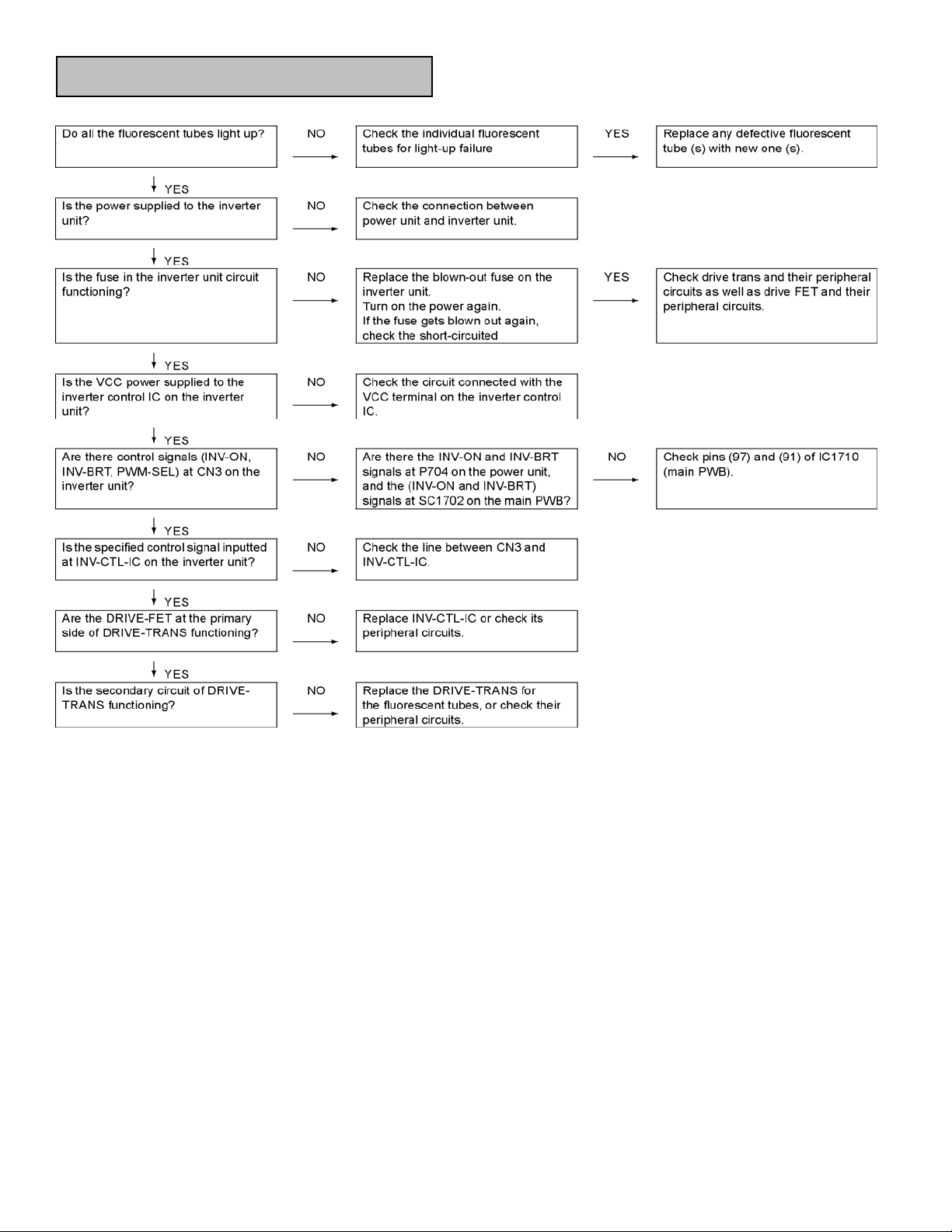
Backlight failure to light up
LC-32WD1E/S/RU and LC-32WT1E
6 - 2
Page 23
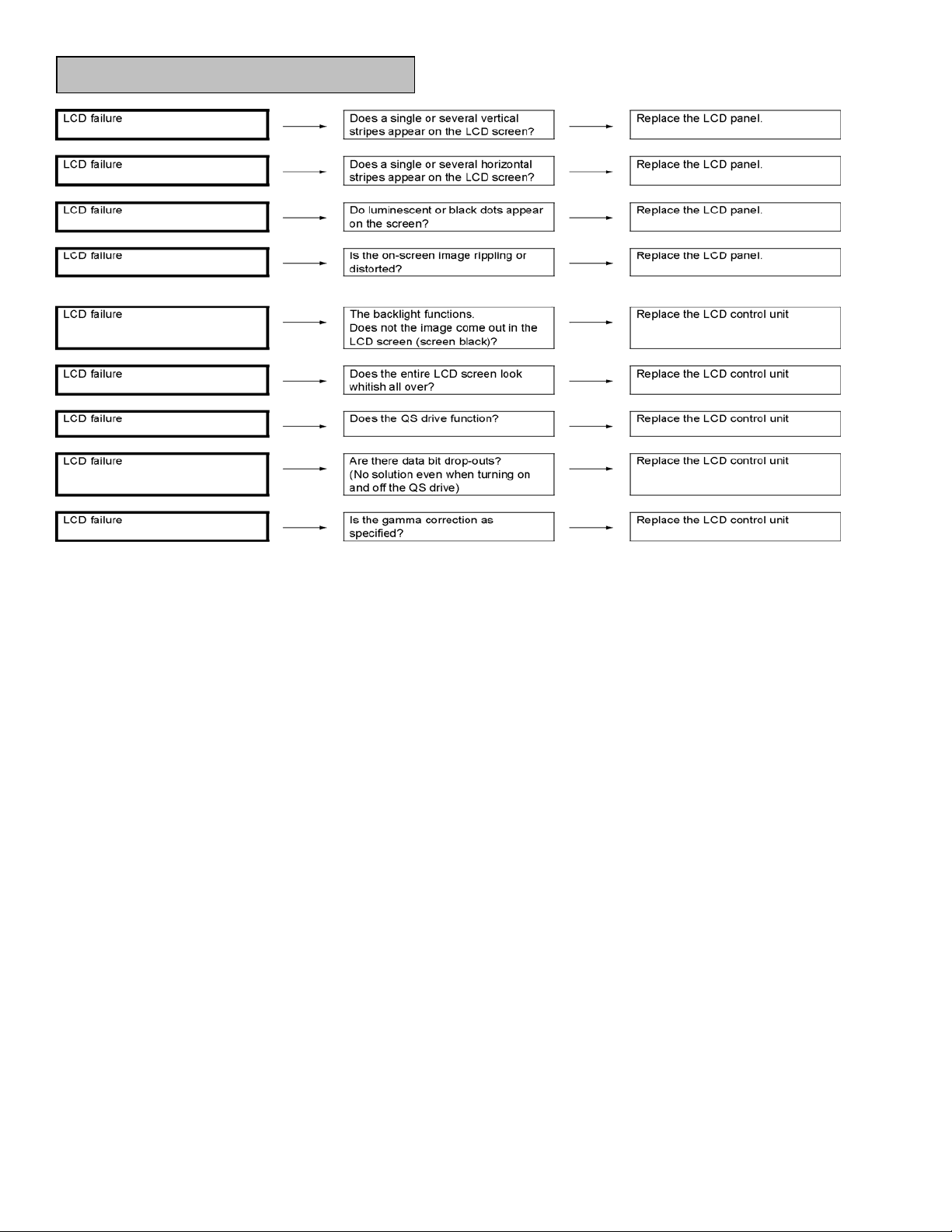
In case of LCD failure:
LC-32WD1E/S/RU and LC-32WT1E
6 - 3
Page 24
NO picture on display via tuner reception (analog TV)
LC-32WD1E/S/RU and LC-32WT1E
6 - 4
No picture appears on LCD screen during tuner reception
Checklist:
1) Is "INPUT SOURCE" button on the remote control set up correctly ? ==> See operation manual and set "INPUT SOURCE" to "TV"
2) Is MENU-PICTURE-Contrast/Brightness set to "MIN" ? ==> Set it to appropriate level
3) Is ANT-CABLE disconnected or connected improperly? ==> Connect it correctly as per the operation manual
v yes
Check if D0911 (LD1117DT50) output (pin2) is 5V
IF yes, check if D0918 (MC34063A) output (pin2) is 6v6
IF yes, check +12V_DVB
These are I2c communication lines for tuner control.
Follow the path and check whether they are forced to LOW.
Check I2C switch D016
Check analog switch D0111 (74HCT1G66PW)
power supply (5V) and functionality
Check the tuner (U011) and peripheral circuits
check video SAW filter and peripheral circuits
check SAW_SW signal
TDA15134E (UOCV) (D013) is not functioning normal,
check GTV SW and peripherals (power supply,xtal,…) of D013
check resistor networks on UOCV_DV signals
Is level of tuner supply voltage (pin 7 of tuner U011) 5V ?
v yes
Is level of I2C lines (pins 4 and 5 of tuner U011) LOW ?
v no
Is level of tuner AGC (pin2 of U011) 0V ?
v no
Is the video signal (IF) sent from pin8 of tuner (U011) ?
v yes
Is video signal sent from pins 4 and 5 of video SAW filter (Z011)
v yes
Is TDA15134E (D013) UOCV_DVCLK clock there
AND are the UOCV_DV(x) signals toggling?
v yes
are UOCV_DV(x) and UOCV_DVCLK signals arriving to
the CPLD (D080) (XC2C128-7TQG144C) ?
v yes
no
yes
yes
no
no
no
no
GOTO VIDEO PATH CHECK
Page 25
NO picture on display via EXT-1 CVBS input
LC-32WD1E/S/RU and LC-32WT1E
6 - 5
No picture on LCD screen when EXT-1 CVBS input source selected
Checklist:
1) Is "INPUT SOURCE" button on the remote control set up correctly ? ==> See operation manual and set "INPUT SOURCE" to "EXT1"
2) Is MENU-PICTURE-Contrast/Brightness set to "MIN" ? ==> Set it to appropriate level
3) Check connection to external device ==> Connect it correctly as per the operation manual for the device
v yes
Check external connection, input setting, SCART1 and peripheral
Is composite video signal arriving to pin20A of SCART1 (X027-1) ?
v yes
Is CVBS signal present on both sides of C0132 ?
v yes
Is TDA15134E (D013) UOCV_DVCLK clock there
AND are the UOCV_DV(x) signals toggling?
v yes
are UOCV_DV(x) and UOCV_DVCLK signals arriving to
the CPLD (D080) (XC2C128-7TQG144C) ?
v yes
no
no
no
no
circuits.
check C0132, check peripheral on SCART1_CVBS_IN signal
(termination R, ESD protection diode,…)
TDA15134E (UOCV) (D013) is not functioning normal,
check GTV SW and peripherals (power supply,xtal,…) of D013
check resistor networks on UOCV_DV signals
GOTO VIDEO PATH CHECK
Page 26
NO picture on display via EXT-1 RGB input
LC-32WD1E/S/RU and LC-32WT1E
6 - 6
No picture on LCD screen when EXT-1 RGB input source selected
Checklist:
1) Is "INPUT SOURCE" button on the remote control set up correctly ? ==> See operation manual and set "INPUT SOURCE" to "EXT1"
2) Is MENU-PICTURE-Contrast/Brightness set to "MIN" ? ==> Set it to appropriate level
3) Check connection to external device ==> Connect it correctly as per the operation manual for the device
v yes
Are RGB signals arriving to pins 15A(R), 11A(G) and 7A(B)
of SCART1 (X027-1) ?
v yes
are RGB signals arriving to video switch TDA8601 (D1301)
at pins 8, 7 and 6 ?
v yes
are RGB signals arriving to both sides of C0177(R), C0175(G) and
C0164(B) ?
v yes
Is TDA15134E (D013) UOCV_DVCLK clock there
AND are the UOCV_DV(x) signals toggling?
v yes
are UOCV_DV(x) and UOCV_DVCLK signals arriving to
the CPLD (D080) (XC2C128-7TQG144C) ?
v yes
Check external connection, input setting, SCART1 and peripheral
no
no
no
no
no
check C1322(R), C1318(G), C1314(B) and check peripheral on
SCART1_RGB signals (termination R, ESD protection diode,…)
Check video switch TDA8601 (D1301) power supply (+8V_SW) and
Check if SLCT_RGB_YPbPr is set correctly
TDA15134E (UOCV) (D013) is not functioning normal,
check GTV SW and peripherals (power supply,xtal,…) of D013
check resistor networks on UOCV_DV signals
circuits.
peripherals
GOTO VIDEO PATH CHECK
Page 27
NO picture on display via EXT-1 Y/C input
LC-32WD1E/S/RU and LC-32WT1E
6 - 7
No picture on LCD screen when EXT-1 Y/C input source selected
Checklist:
1) Is "INPUT SOURCE" button on the remote control set up correctly ? ==> See operation manual and set "INPUT SOURCE" to "EXT1"
2) Is MENU-PICTURE-Contrast/Brightness set to "MIN" ? ==> Set it to appropriate level
3) Check connection to external device ==> Connect it correctly as per the operation manual for the device
v yes
Are Y/C signals arriving to pins 20A(Y) and 15A(C)
of SCART1 (X027-1) ?
v yes
is C signal arriving to video switch TDA8601 (D1301)
at pin 8 ?
v yes
are Y/C signals arriving to both sides of C0177(C) and C0132(Y) ?
v yes
Is TDA15134E (D013) UOCV_DVCLK clock there
AND are the UOCV_DV(x) signals toggling?
v yes
are UOCV_DV(x) and UOCV_DVCLK signals arriving to
the CPLD (D080) (XC2C128-7TQG144C) ?
v yes
Check external connection, input setting, SCART1 and peripheral
no
check C1322 and check peripheral on SCART1_R signal (termination
no
Check video switch TDA8601 (D1301) power supply (+8V_SW) and
no
no
peripherals, Check if SLCT_RGB_YPbPr is set correctly.
Check C0132, check peripheral on SCART1_CVBS_IN signal
TDA15134E (UOCV) (D013) is not functioning normal,
check GTV SW and peripherals (power supply,xtal,…) of D013
no
R, ESD protection diode,…)
(termination R, ESD protection diode,…)
check resistor networks on UOCV_DV signals
circuits.
GOTO VIDEO PATH CHECK
Page 28

NO picture on display via EXT-2 CVBS input
LC-32WD1E/S/RU and LC-32WT1E
6 - 8
No picture on LCD screen when EXT-2 CVBS input source selected
Checklist:
1) Is "INPUT SOURCE" button on the remote control set up correctly ? ==> See operation manual and set "INPUT SOURCE" to "EXT2"
2) Is MENU-PICTURE-Contrast/Brightness set to "MIN" ? ==> Set it to appropriate level
3) Check connection to external device ==> Connect it correctly as per the operation manual for the device
v yes
Check external connection, input setting, SCART2 and peripheral
Is composite video signal arriving to pin20B of SCART2 (X027-2) ?
v yes
Is CVBS signal present on both sides of C0169 ?
v yes
Is TDA15134E (D013) UOCV_DVCLK clock there
AND are the UOCV_DV(x) signals toggling?
v yes
are UOCV_DV(x) and UOCV_DVCLK signals arriving to
the CPLD (D080) (XC2C128-7TQG144C) ?
v yes
no
check C0169, check peripheral on SCART2_Y_CVBS_IN signal
no
no
no
check GTV SW and peripherals (power supply,xtal,…) of D013
(termination R, ESD protection diode,…)
TDA15134E (UOCV) (D013) is not functioning normal,
check resistor networks on UOCV_DV signals
circuits.
GOTO VIDEO PATH CHECK
Page 29
NO picture on display via EXT-2 RGB input
LC-32WD1E/S/RU and LC-32WT1E
6 - 9
No picture on LCD screen when EXT-2 RGB input source selected
Checklist:
1) Is "INPUT SOURCE" button on the remote control set up correctly ? ==> See operation manual and set "INPUT SOURCE" to "EXT2"
2) Is MENU-PICTURE-Contrast/Brightness set to "MIN" ? ==> Set it to appropriate level
3) Check connection to external device ==> Connect it correctly as per the operation manual for the device
v yes
Are RGB signals arriving to pins 15B(R), 11B(G) and 7B(B)
of SCART2 (X027-2) ?
v yes
are RGB signals arriving to video switch TDA8601 (D1302)
at pins 8, 7 and 6 ?
v yes
are RGB signals arriving to both sides of C0178(R), C0176(G) and
C0165(B) ?
v yes
Is TDA15134E (D013) UOCV_DVCLK clock there
AND are the UOCV_DV(x) signals toggling?
v yes
are UOCV_DV(x) and UOCV_DVCLK signals arriving to
the CPLD (D080) (XC2C128-7TQG144C) ?
v yes
Check external connection, input setting, SCART2 and peripheral
no
check C1338(R), C1334(G), C1331(B) and check peripheral on
SCART2_RGB signals (termination R, ESD protection diode,…)
no
Check video switch TDA8601 (D1302) power supply (+8V_SW) and
no
no
no
check GTV SW and peripherals (power supply,xtal,…) of D013
Check if SLCT_RGB_YPbPr is set correctly
TDA15134E (UOCV) (D013) is not functioning normal,
check resistor networks on UOCV_DV signals
circuits.
peripherals
GOTO VIDEO PATH CHECK
Page 30

NO picture on display via EXT-2 Y/C input
LC-32WD1E/S/RU and LC-32WT1E
6 - 10
No picture on LCD screen when EXT-2 Y/C input source selected
Checklist:
1) Is "INPUT SOURCE" button on the remote control set up correctly ? ==> See operation manual and set "INPUT SOURCE" to "EXT2"
2) Is MENU-PICTURE-Contrast/Brightness set to "MIN" ? ==> Set it to appropriate level
3) Check connection to external device ==> Connect it correctly as per the operation manual for the device
v yes
Are Y/C signals arriving to pins 20B(Y) and 15B(C)
of SCART2 (X027-2) ?
v yes
is C signal arriving to video switch TDA8601 (D1302)
at pin 8 ?
v yes
are Y/C signals arriving to both sides of C0178(C) and C0169(Y) ?
v yes
Is TDA15134E (D013) UOCV_DVCLK clock there
AND are the UOCV_DV(x) signals toggling?
v yes
are UOCV_DV(x) and UOCV_DVCLK signals arriving to
the CPLD (D080) (XC2C128-7TQG144C) ?
v yes
Check external connection, input setting, SCART2 and peripheral
no
no
no
no
no
check C1338 and check peripheral on SCART2_R_C signal
(termination R, ESD protection diode,…)
Check video switch TDA8601 (D1302) power supply (+8V_SW) and
peripherals, Check if SLCT_RGB_YPbPr is set correctly.
Check C0169, check peripheral on SCART2_Y_CVBS_IN signal
(termination R, ESD protection diode,…)
TDA15134E (UOCV) (D013) is not functioning normal,
check GTV SW and peripherals (power supply,xtal,…) of D013
check resistor networks on UOCV_DV signals
circuits.
GOTO VIDEO PATH CHECK
Page 31
NO picture on display via EXT-3 CVBS input
LC-32WD1E/S/RU and LC-32WT1E
6 - 11
No picture on LCD screen when EXT-3 CVBS input source selected
Checklist:
1) Is "INPUT SOURCE" button on the remote control set up correctly ? ==> See operation manual and set "INPUT SOURCE" to "EXT3"
2) Is MENU-PICTURE-Contrast/Brightness set to "MIN" ? ==> Set it to appropriate level
3) Check connection to external device ==> Connect it correctly as per the operation manual for the device
v yes
Is composite video signal arriving to pin1 of connector X014 on Side
I/O PCB ?
v yes
Is CVBS signal present on pin1 of X0208 on Main PCB ?
v yes
Is CVBS signal present on both sides of C01100 ?
v yes
Is TDA15134E (D013) UOCV_DVCLK clock there
AND are the UOCV_DV(x) signals toggling?
v yes
are UOCV_DV(x) and UOCV_DVCLK signals arriving to
the CPLD (D080) (XC2C128-7TQG144C) ?
v yes
Check external connection, input setting, connector X011-2 and
no
no
no
no
no
peripheral circuits (termination R, ESD protection diode,…)
Check connectors X014 on side I/O PCB and X0208 on
Main PCB, check wiring between these connectors.
check C01100, check peripheral on FRONT_Y_CVBS_IN signal
(termination R, BLM,…)
TDA15134E (UOCV) (D013) is not functioning normal,
check GTV SW and peripherals (power supply,xtal,…) of D013
check resistor networks on UOCV_DV signals
GOTO VIDEO PATH CHECK
Page 32

NO picture on display via EXT-3 Y/C input
LC-32WD1E/S/RU and LC-32WT1E
6 - 12
No picture on LCD screen when EXT-3 Y/C input source selected
Checklist:
1) Is "INPUT SOURCE" button on the remote control set up correctly ? ==> See operation manual and set "INPUT SOURCE" to "EXT3"
2) Is MENU-PICTURE-Contrast/Brightness set to "MIN" ? ==> Set it to appropriate level
3) Check connection to external device ==> Connect it correctly as per the operation manual for the device
v yes
Are Y/C video signals arriving to pin1(Y) and pin3(C) of connector
X014 on Side I/O PCB ?
v yes
Are Y/C signals present on pin1 and pin3 of X0208 on Main PCB ?
v yes
Are Y/C signals present on both sides of C01100(Y) and
C0168(C) ?
v yes
Is TDA15134E (D013) UOCV_DVCLK clock there
AND are the UOCV_DV(x) signals toggling?
v yes
are UOCV_DV(x) and UOCV_DVCLK signals arriving to
the CPLD (D080) (XC2C128-7TQG144C) ?
v yes
Check external connection, input setting, connector X011-1 and
no
no
no
no
no
peripheral circuits (termination R, ESD protection diode,…)
Check connectors X014 on side I/O PCB and X0208 on
Main PCB, check wiring between these connectors.
check C01100 and C0168, check peripherals on FRONT_Y_CVBS_IN
and FRONT_C_IN signals
(termination R, BLM,…)
TDA15134E (UOCV) (D013) is not functioning normal,
check GTV SW and peripherals (power supply,xtal,…) of D013
check resistor networks on UOCV_DV signals
GOTO VIDEO PATH CHECK
Page 33

NO picture on display via EXT-4 (YPbPr) input
LC-32WD1E/S/RU and LC-32WT1E
6 - 13
No picture on LCD screen when EXT-4 YPbPr input source selected
Checklist:
1) Is "INPUT SOURCE" button on the remote control set up correctly ? ==> See operation manual and set "INPUT SOURCE" to "EXT4"
2) Is MENU-PICTURE-Contrast/Brightness set to "MIN" ? ==> Set it to appropriate level
3) Check connection to external device ==> Connect it correctly as per the operation manual for the device
4) check if supported format is connected to EXT4
v yes
Are YPbPr signals arriving to pins 6(Y), 4(Pb) and 2(PR) on
connector X0215 ?
v yes
1. HD patch check
Check external connection, input setting, YPbPr connector and
no
peripheral circuits.
are YPbPr signals arriving to video switch TDA8601 (D1301)
at pins 3(Y), 2(Pb) and 4(Pr) ?
v yes
are YPbPr signals arriving to TDA9975AEL/10(D030), check on
capacitors: C033(Y), C034(Pb) and C030(Pr) ?
v yes
Is Hirate_MCLK 13,5MHz clock present on R0368 ?
v yes
Is TDA9975AEL/10(D030) Hirate_CLK clock there on R0325?,
are the CS (R0328), HS (R0330) and VS (R0331) signals there ?
AND are the VPA(x), VPB(x) and VPC(X) signals toggling on the
network resistors R030-R034 and on R0310-R0318?
v yes
GOTO VIDEO PATH CHECK
2. SD patch check
are YPbPr signals arriving to both sides of C0177(Pr), C0175(Y) and
C0164(Pb) ?
v yes
Is TDA15134E (D013) UOCV_DVCLK clock there
AND are the UOCV_DV(x) signals toggling?
v yes
are UOCV_DV(x) and UOCV_DVCLK signals arriving to
the CPLD (D080) (XC2C128-7TQG144C) ?
v yes
check C1317(Y), C1313(Pb), C1321(Pr) and check other peripheral
no
check YPbPr signals peripheral circuits (termination resistors, buffers
no
Check PNX5010E (D040) SW and its peripherals (power supply,
no
no
Check video switch TDA8601 (D1301) power supply (+8V_SW) and
no
no
no
V030,V031,V032 and other peripheral circuits)
TDA9975AEL/10 (Hirate) (D030) is not functioning normal,
check PNX SW, check if TM_SCL and TM_SDA are functioning
normal and check other peripherals (power supply,…) of D030
Check if SLCT_RGB_YPbPr is set correctly
TDA15134E (UOCV) (D013) is not functioning normal,
check GTV SW and peripherals (power supply,xtal,…) of D013
check resistor networks on UOCV_DV signals
circuits on YPbPr signals
XTAL,….)
peripherals
GOTO VIDEO PATH CHECK
Page 34

NO picture on display via EXT-5 (VGA) input
A
LC-32WD1E/S/RU and LC-32WT1E
6 - 14
No picture on LCD screen when EXT-5 (15pin D-SUB terminal) input
Checklist:
1) Is "INPUT SOURCE" button on the remote control set up correctly ? ==> See operation manual and set "INPUT SOURCE" to "EXT5"
2) Is MENU-PICTURE-Contrast/Brightness set to "MIN" ? ==> Set it to appropriate level
3) Check connection to external device ==> Connect it correctly as per the operation manual for the device
4) Check if supported format is connected to EXT5.
Are the VGA RGB video signals and H and V sync signals present
on pins 1(R), 2(G), 3(G) 13(H) and 14(V) on connector X070 on main
Are VGA_RGB signals present on both side of C071(R),
re H and V-sync signals present on both sides of R070(H sync) and
Is Hirate_MCLK 13,5MHz clock present on R0368 ?
Is TDA9975AEL/10(D030) Hirate_CLK clock there on R0325?,
are the CS (R0328), HS (R0330) and VS (R0331) signals there ?
AND are the VPA(x), VPB(x) and VPC(X) signals toggling on the
network resistors R030-R034 and on R0310-R0318?
source selected
v yes
PCB ?
v yes
C0380(G) and C072(B)?
v yes
R0730(V sync) ?
v yes
v yes
v yes
Check VGA (D-SUB-15) connector X070 and external connection.
no
no
no
no
no
Check peripheral circuits on the VGA_R, VGA_G and VGA_B
signals.
Check peripheral circuits on the VGA_HSYNC and VGA_CSYNC
signals.
Check PNX5010E (D040) SW and its peripherals (power supply,
XTAL,….)
TDA9975AEL/10 (Hirate) (D030) is not functioning normal,
check PNX SW, check if TM_SCL and TM_SDA are functioning
normal and check other peripherals (power supply,…) of D030
GOTO VIDEO PATH CHECK
Page 35

NO picture on display via EXT-6 (HDMI1) input
LC-32WD1E/S/RU and LC-32WT1E
6 - 15
No picture on LCD screen when EXT-6 (HDMI1) input source
Checklist:
1) Is "INPUT SOURCE" button on the remote control set up correctly ? ==> See operation manual and set "INPUT SOURCE" to "EXT6"
2) Is MENU-PICTURE-Contrast/Brightness set to "MIN" ? ==> Set it to appropriate level
3) Check connection to external device ==> Connect it correctly as per the operation manual for the device
4) Check if supported format is connected to EXT6. ==> (720p, 1080i, …)
5) Is correct video signal type applied from external HDMI device ? ==> Confirm the type (it should be "RGB", "YCbCr 4:4:4" or "YCbCr 4:2:2")
6) Is correct color matrix applied from external HDMI device ? ==> Confirm the type (it should be "ITU601" or "ITU709")
Are the HDMI signals ARX(+-) present on pins 1-12 on connector
Are the HDMI signals PARX(+-) present on both sides of the
commonmode chokes Z070, Z071, Z074 and Z075 ?
Are I2C signals (ARX_DDC_SDA and ARX_DDC_SCL) present on
EDID eeprom M24C02 (D071) pins 5 and 6 ?
Is Hirate_MCLK 13,5MHz clock present on R0368 ?
Is TDA9975AEL/10(D030) Hirate_CLK clock there on R0325?,
are the CS (R0328), HS (R0330) and VS (R0331) signals there ?
AND are the VPA(x), VPB(x) and VPC(X) signals toggling on the
network resistors R030-R034 and on R0310-R0318?
selected
v yes
X072 on main PCB ?
v yes
v yes
v yes
v yes
v yes
no
no
no
no
no
Check HDMI connector X072 and external connection.
Check commonmode chokes.
Check peripheral circuits on ARX_DDC_SDA/SCL and
PARX_DDC_SDA/SCL signals.
Check PNX5010E (D040) SW and its peripherals (power supply,
XTAL,….)
TDA9975AEL/10 (Hirate) (D030) is not functioning normal,
check PNX SW, check if TM_SCL and TM_SDA are functioning
normal and check other peripherals (power supply,…) of D030
GOTO VIDEO PATH CHECK
Page 36

NO picture on display via EXT-7 (HDMI2) input
LC-32WD1E/S/RU and LC-32WT1E
6 - 16
No picture on LCD screen when EXT-7 (HDMI2) input source
Checklist:
1) Is "INPUT SOURCE" button on the remote control set up correctly ? ==> See operation manual and set "INPUT SOURCE" to "EXT7"
2) Is MENU-PICTURE-Contrast/Brightness set to "MIN" ? ==> Set it to appropriate level
3) Check connection to external device ==> Connect it correctly as per the operation manual for the device
4) Check if supported format is connected to EXT7. ==> (720p, 1080i, …)
5) Is correct video signal type applied from external HDMI device ? ==> Confirm the type (it should be "RGB", "YCbCr 4:4:4" or "YCbCr 4:2:2")
6) Is correct color matrix applied from external HDMI device ? ==> Confirm the type (it should be "ITU601" or "ITU709")
Are the HDMI signals BRX(+-) present on pins 1-12 on connector
Are the HDMI signals PBRX(+-) present on both sides of the
commonmode chokes Z0712, Z0714, Z0715 and Z0716 ?
Are I2C signals (BRX_DDC_SDA and BRX_DDC_SCL) present on
EDID eeprom M24C02 (D0705) pins 5 and 6 ?
Is Hirate_MCLK 13,5MHz clock present on R0368 ?
Is TDA9975AEL/10(D030) Hirate_CLK clock there on R0325?,
are the CS (R0328), HS (R0330) and VS (R0331) signals there ?
AND are the VPA(x), VPB(x) and VPC(X) signals toggling on the
network resistors R030-R034 and on R0310-R0318?
selected
v yes
X073 on main PCB ?
v yes
v yes
v yes
v yes
v yes
no
no
no
no
no
Check HDMI connector X073 and external connection.
Check commonmode chokes.
Check peripheral circuits on BRX_DDC_SDA/SCL and
PBRX_DDC_SDA/SCL signals.
Check PNX5010E (D040) SW and its peripherals (power supply,
XTAL,….)
TDA9975AEL/10 (Hirate) (D030) is not functioning normal,
check PNX SW, check if TM_SCL and TM_SDA are functioning
normal and check other peripherals (power supply,…) of D030
GOTO VIDEO PATH CHECK
Page 37

NO picture on Monitor out via tuner reception
LC-32WD1E/S/RU and LC-32WT1E
6 - 17
SCART1:
No picture appears on EXT-1 - connected monitor
during tuner reception
Checklist:
1) Are input terminal on back of TV and "INPUT SOURCE" button on the remote control set up correctly ?
==> See operation manual and set "INPUT SOURCE" appropriatly
2) is the signal type (item) in MENU - OPTION - Input Slect equal to signal type of an external device ?
==> set it to "CVBS", "Y/C" or "RGB".
3) Is ANT-CABLE disconnected or connected improperly? ==> Connect it correctly as per the operation manual
4) The picture is sent to the monitor in a CVBS signal if the source during display is TV,CVBS or Y/C of EXT1-3.
When sent by component, etc., that signal is not sent to the monitor.
5) When the monitor picture is not sent and is not displayed on the monitor, refer to "NO picture on display" for each terminal.
6) The video output from EXT1 is not the monitor output (output of the picture now watching).
The picture of the last selected TV channel is always sent to EXT1. (specification)
v yes
Is video signal (CVBS) sent to pin19A of SCART1 (X027-1) ?
v no
Is video signal (CVBS) sent to R1371 ?
v no
TDA15143E (D013) is not functioning normal.
Is tuner reception visible on LCD screen ?
v no
yes
yes
yes
Check SCART1, external connection or input setting.
Check +5V_TV, check buffer peripherals (V1332, V1331)
and check ESD protection diode (V1315) short to GND ?
Check R0124
Check TDA15143E (D013) peripherals or GTV SW
GOTO "NO picture on display via tuner reception (analog TV)"
Page 38

NO picture on Monitor out via EXT-1
LC-32WD1E/S/RU and LC-32WT1E
6 - 18
SCART2:
No picture from EXT-1 appears on EXT-2 - connected monitor
Note: EXT2 has always the same picture as the picture on the
LCD screen
Checklist:
1) Are input terminal on back of TV and "INPUT SOURCE" button on the remote control set up correctly ?
==> See operation manual and set "INPUT SOURCE" appropriatly
2) is the signal type (item) in MENU - OPTION - Input Slect equal to signal type of an external device ?
==> set it to "CVBS", "Y/C" or "RGB".
3) Is ANT-CABLE disconnected or connected improperly? ==> Connect it correctly as per the operation manual
4) The picture is sent to the monitor in a CVBS signal if the source during display is TV,CVBS or Y/C of EXT1-3.
When sent by component, etc., that signal is not sent to the monitor.
5) When the monitor picture is not sent and is not displayed on the monitor, refer to "NO picture on display" for each terminal.
6) The video output from EXT1 is not the monitor output (output of the picture now watching).
The picture of the last selected TV channel is always sent to EXT1. (specification)
v yes
Is video signal (CVBS) sent to pin19B of SCART2 (X027-2) ?
v no
Is video signal (CVBS) sent to R01188 ?
v no
Is EXT1 input visible on LCD screen ?
v no
yes
yes
yes
Check SCART2, external connection or input setting.
Check +5V_TV, check buffer peripherals (V1321, V1330)
and check ESD protection diode (V1322) short to GND ?
Check TDA15143E (D013) peripherals or GTV SW
GOTO "NO picture on display via EXT-1"
Page 39
NO picture on Monitor out via EXT-3
LC-32WD1E/S/RU and LC-32WT1E
6 - 19
SCART2:
No picture from EXT-3 appears on EXT-2 - connected monitor
Checklist:
1) Are input terminal on back of TV and "INPUT SOURCE" button on the remote control set up correctly ?
==> See operation manual and set "INPUT SOURCE" appropriatly
2) is the signal type (item) in MENU - OPTION - Input Slect equal to signal type of an external device ?
==> set it to "CVBS", "Y/C" or "RGB".
3) Is ANT-CABLE disconnected or connected improperly? ==> Connect it correctly as per the operation manual
4) The picture is sent to the monitor in a CVBS signal if the source during display is TV,CVBS or Y/C of EXT1-3.
When sent by component, etc., that signal is not sent to the monitor.
5) When the monitor picture is not sent and is not displayed on the monitor, refer to "NO picture on display" for each terminal.
6) The video output from EXT1 is not the monitor output (output of the picture now watching).
The picture of the last selected TV channel is always sent to EXT1. (specification)
v yes
Is video signal (CVBS) sent to pin19B of SCART2 (X027-2) ?
v no
Is video signal (CVBS) sent to R01188 ?
v no
Is EXT3 input visible on LCD screen ?
v no
yes
yes
yes
Check SCART2, external connection or input setting.
Check +5V_TV, check buffer peripherals (V1321, V1330)
and check ESD protection diode (V1322) short to GND ?
Check TDA15143E (D013) peripherals or GTV SW
GOTO "NO picture on display via EXT-3"
Page 40

VIDEO PATH CHECK
LC-32WD1E/S/RU and LC-32WT1E
6 - 20
are VDI_D(x) signals arriving to PNX5010E (D040) ?
v yes
are VDO_D(x) signals and CLK signal arriving to LVDS transmitter
D061 ?
v yes
are LVDS signals arriving to common mode chokes (Z060 - Z061 -
Z062 - Z063 - Z064) ?
v yes
are LVDS signals arriving to LVDS connector (X060) ?
v yes
is LVDS_POWER available at the LVDS connector (X060) ?
v yes
are LVDS power and LVDS signals available on
the LCD control unit ?
v yes
Is backlight ON ?
v yes
no
no
no
no
no
no
no
check CPLD (D080) power levels, peripherals, CPLD code
PNX5010E (D040) is not functioning normal, check PNX SW,
DDR-SDRAM, XTAL, power supply and other peripheral
check pin32 of D061 (power_down?) => check D063 signals and
peripherals, check other LVDS transmitter peripherals
check common mode chokes (Z060 - Z064)
Is +12V available ? NO => check PSU
YES => check DC/DC converter, check panel_power_enable signal
and peripherals
check LVDS wiring
GO TO backlight Faillure
replace LCD control unit
Page 41
No audio output during UHF/VHF reception
LC-32WD1E/S/RU and LC-32WT1E
6 - 21
Is the set unmuted?
v yes
Is the volume set to "50"
v yes
Are headphones disconnected from the set?
v yes
Is the antenna properly connected?
v yes
Is audio signal sent from D013 (TDA15134)?
Check R0155 and R0158
v yes
Is audio signal sent from D020 (TDA8932)?
Check D020-27/30 and D020-19/22
v yes
Is audio signal on X022 and X021 normal
v yes
no
no
no
no
no
Is the audio signal (SIF) sent from the Tuner U011?
no
no
press the "mute" on the remote
press the "volume up" on the remote
until volume is "50"
remove the headphones plug from the set
Connect according to manual
Is the audio signal (SIF) sent to D013
Check Z010-4 and Z010-5
v no
Check U011-8
v no
Check 5V_tuner, AGC and I2C signals
Fixed?
v no
Replace tuner
Check +28V_audio and other D020 circuitery
Check connectors
Check +8V_TV(C019) and +5V_TV(C01113)
yes
Check circuitery of SAW filters (Z010 and
yes
and periferal circuit
Z011)
Check speakers and wiring
Page 42

No Sound from an external input device connected to
LC-32WD1E/S/RU and LC-32WT1E
6 - 22
EXT1 (SCART 1)
Is IN1-L audio signal sent from X027-1-6A (SCART1) to
D022-4 (TEA6422)
Is IN1-R audio signal sent from X027-1-2A (SCART1) to
D022-25 (TEA6422)
v yes
no
Check SCART connector (X027-1) and the cable to
device
Is the audio signal sent from D022-12 and D022-13 to
D013?
Check C0150 and C0152
v yes
Is audio signal sent from D013 (TDA15134)?
Check R0155 and R0158
v yes
Is audio signal sent from D020 (TDA8932)?
Check D020-27/30 and D020-19/22
v yes
Is audio signal on X022 and X021 normal
v yes
Check speakers and wiring
no
no
no
no
Check D022 circuitery (SDA/SCL,…)
Check D013 circitery (R0155, R0158…)
Check +28V_audio and other D020 circuitery
Check connectors
Page 43
No Sound from an external input device connected to
LC-32WD1E/S/RU and LC-32WT1E
6 - 23
EXT2 (SCART 2)
Is IN1-L audio signal sent from X027-2-6B (SCART2) to
D022-5 (TEA6422)
Is IN1-R audio signal sent from X027-2-2B (SCART2) to
D022-24 (TEA6422)
v yes
no
Check SCART connector (X027-2) and the cable to
device
Is the audio signal sent from D022-12 and D022-13 to
D013?
Check C0150 and C0152
v yes
Is audio signal sent from D013 (TDA15134)?
Check R0155 and R0158
v yes
Is audio signal sent from D020 (TDA8932)?
Check D020-27/30 and D020-19/22
v yes
Is audio signal on X022 and X021 normal
v yes
Check speakers and wiring
no
no
no
no
Check D022 circuitery (SDA/SCL,…)
Check D013 circitery (R0155, R0158…)
Check +28V_audio and other D020 circuitery
Check connectors
Page 44

No Sound from an external input device connected to
LC-32WD1E/S/RU and LC-32WT1E
6 - 24
EXT3 (Side IO)
Is the audio signal leaving the SideIO PCB?
Check on pin X014-5 and X014-7
v yes
Is audio signal present on mainboard connector X0208?
Check X0208-5 and X0208-7
v yes
Is audio signal arriving on D013?
Check C0158 and C0159
v yes
Is audio signal sent from D013 (TDA15134)?
Check R0155 and R0158
v yes
Is audio signal sent from D020 (TDA8932)?
Check D020-27/30 and D020-19/22
v yes
Is audio signal on X022 and X021 normal
no
no
no
no
no
no
if audio cable is connected according user manual,
check/replace SideIO
Check/replace cable
Check D010 input circuitery
Check D013 circitery (R0155, R0158…)
Check +28V_audio and other D020 circuitery
Check connectors
v yes
Check speakers and wiring
Page 45

No Sound from an external input device connected to
LC-32WD1E/S/RU and LC-32WT1E
6 - 25
EXT4 (YPbPr-component)
Is YPbPr_L audio signal sent from X0215-10 to D022-6
(TEA6422)
Is YPbPr_R audio signal sent from X0215-8 to D022-23
(TEA6422)
v yes
no
Check connector (X0215) and the cable to device
Is the audio signal sent from D022-12 and D022-13 to
D013?
Check C0150 and C0152
v yes
Is audio signal sent from D013 (TDA15134)?
Check R0155 and R0158
v yes
Is audio signal sent from D020 (TDA8932)?
Check D020-27/30 and D020-19/22
v yes
Is audio signal on X022 and X021 normal
v yes
Check speakers and wiring
no
no
no
no
Check D022 circuitery (SDA/SCL,…)
Check D013 circitery (R0155, R0158…)
Check +28V_audio and other D020 circuitery
Check connectors
Page 46

No Sound from an external input device connected to
LC-32WD1E/S/RU and LC-32WT1E
6 - 26
EXT5 (VGA)
Is PC_IL audio signal sent from X028-2-T to D022-9
(TEA6422)
Is PC_IR audio signal sent from X028-2-R to D022-20
(TEA6422)
v yes
no
Check connector (X028-2) and the cable to device
Is the audio signal sent from D022-12 and D022-13 to
D013?
Check C0150 and C0152
v yes
Is audio signal sent from D013 (TDA15134)?
Check R0155 and R0158
v yes
Is audio signal sent from D020 (TDA8932)?
Check D020-27/30 and D020-19/22
v yes
Is audio signal on X022 and X021 normal
v yes
Check speakers and wiring
no
no
no
no
Check D022 circuitery (SDA/SCL,…)
Check D013 circitery (R0155, R0158…)
Check +28V_audio and other D020 circuitery
Check connectors
Page 47

No Sound from an external input device connected to
LC-32WD1E/S/RU and LC-32WT1E
6 - 27
EXT6 (DVI-adapter connected to HDMI1)
Is HDMI_IL audio signal sent from X028-1-T to D022-10
(TEA6422)
Is HDMI_IR audio signal sent from X028-1-R to D022-19
(TEA6422)
v yes
no
Check connector (X028-1) and the cable to device
Is a DVI source connected to the HDMI1 connector?
(using an adapter)
v yes
Is the audio signal sent from D022-12 and D022-13 to
D013?
Check C0150 and C0152
v yes
Is audio signal sent from D013 (TDA15134)?
Check R0155 and R0158
v yes
Is audio signal sent from D020 (TDA8932)?
Check D020-27/30 and D020-19/22
v yes
Is audio signal on X022 and X021 normal
v yes
Check speakers and wiring
Connect DVI source (Set will only switch to analog audio
no
no
no
no
no
Check +28V_audio and other D020 circuitery
when DVI signal is applied)
Check D022 circuitery (SDA/SCL,…)
Check D013 circitery (R0155, R0158…)
Check connectors
Page 48
No Sound from an external input device connected to
LC-32WD1E/S/RU and LC-32WT1E
6 - 28
EXT6/7 (HDMI1/2)
Do you see the HDMI content displayed on the screen
v yes
Is audio signal sent from D013 (TDA15134)?
Check R0155 and R0158
v yes
Is audio signal sent from D020 (TDA8932)?
Check D020-27/30 and D020-19/22
v yes
Is audio signal on X022 and X021 normal
v yes
Check speakers and wiring
no
no
no
no
see no video on EXT6/7
Check D013 circitery (R0155, R0158…)
Check +28V_audio and other D020 circuitery
Check connectors
Page 49

No sound except from speakers
LC-32WD1E/S/RU and LC-32WT1E
6 - 29
Audio output from the headphones
Is audio signal sent from D013 (TDA15134)?
Check R0151 and R0152
v yes
Is audio signal sent from D023 (TDA1308)?
Check TP0286 and TP0288
v yes
Is audio signal present on mainboard conn X0208?
Check X0208-9 and X0208-11
v yes
Is the audio signal arriving on the SideIO PCB?
Check on pin X014-11 and X014-12
v yes
Is the audio signal on the headphone terminal?
On SideIO PCB, connector X011-5
v yes
Check headphones
no
no
no
no
no
Check D013 circitery (R0151, R0152…)
Check D023 circuitery
Check V0213, V0216, Z0229 and Z0230
Check/replace cable
replace/check SideIO
Page 50

No sound except from speakers
LC-32WD1E/S/RU and LC-32WT1E
6 - 30
Audio output from EXT1
Is audio signal sent from D013 (TDA15134)?
Check R0160 and R0162
v yes
Is audio signal arriving on X027 (SCART1)?
Check X027-1A and X027-3A
v yes
Check SCART cable
no
no
Check D013 circitery (R0160, R0162…)
Check connector/circuitery
Page 51

No sound except from speakers
LC-32WD1E/S/RU and LC-32WT1E
6 - 31
Audio output from EXT2
Is audio signal sent from D013 (TDA15134)?
Check R01150 and R01151
v yes
Is audio signal arriving on X027-2 (SCART2)?
Check X027-2-1B and X027-2-3B
v yes
Check SCART cable
no
no
Check D013 circitery (R01150, R01151…)
Check connector/circuitery and R01203, R01209
Page 52

No sound except from speakers
LC-32WD1E/S/RU and LC-32WT1E
6 - 32
Audio output from Line Out
Is audio signal sent from D013 (TDA15134)?
Check R01150 and R01151
v yes
Is audio signal arriving on X0215?
Check X0215-12 and X0215-14
v yes
Audio cables
no
no
Check D013 circitery (R01150, R01151…)
Check connector/circuitery and R01215, R01216
Page 53

DTV troubelshooting
y
y
y
LC-32WD1E/S/RU and LC-32WT1E
6 - 33
The unit does not enter the DTV mode or the DVT menu
does not appear
v no
No video output during DTV reception
v no
No audio output during DTV reception
es
es
es
See section: "Does not enter DTV mode"
See section: "No video output on DTV"
See section: "No Audio output on DTV"
Page 54

The unit does not enter the DTV mode or the DVT menu
y
LC-32WD1E/S/RU and LC-32WT1E
6 - 34
does not appear
Does LED H1101 flash on-off?
v no
Is 12V_DVB supplied to D1006-8
v yes
Check voltages:
+5VD on D1006-1
+3V3D on D1005-5
+2V5D on D1002-5
+1V2D on D1003-5
+1VD on D004-5
v yes
Do G1101 and G1001 oscillate?
v yes
Check +5V_tuner on U011-7
v yes
es
no
no
no
no
SW is running, check "No video output on DTV"
check if 12V is on R0978 and R08979. If not, PSU
problem
check circuit of corresponding DC/DC of LDO
Check periferal circuits of G1101and G1001
Check periferal circuits of D0911
Is pin D016-13 high level? (I2C select)
v yes
Check I2C data/clk on tuner pins U011-4 and U011-5
v yes
Check D1001 (demod) and D1101 periferal circuits
no
no
Check circuit of D018 (inverter) and D1410 (Atmel)
Check D1001 (demod) and D1101-4 and D1101-5
Page 55
No video output during DTV reception
LC-32WD1E/S/RU and LC-32WT1E
6 - 35
Is transport stream from D1001 to D1101 present?
Check: D1001-33,35,36,37,39,40,42,43,44,46,47
v yes
Is a smartcard inserted in the Common Interface
connector
v yes v yes
Check if TS_SWITCH = High
v yes v yes
Check D1101-120 periferal circuitery
no
no
no
Check resistor networks: R1037, R1038
Check resistors: R1034,R1035 and R1036
Check if TS_SWITCH = High
Is transport stream on the output of D1212, D1213 and
D1214
Is transport stream on input of D1101-
38,39,40,41,43,44,45,33,34,35,36
v yes
Is video (YPbPr and CVBS) measured on D1107
inputs?
v yes
Is video (YPbPr and CVBS) measured on D1302
inputs? (D1302-2,D1302-3 and D1302,4)
v yes
Is a LOW level on SLCT_RGB_YPbPr?
Check D1302-5
v yes
Is video measured on input of D010?
Check: C0178, C0176, C0165
v yes
check resistor networks: R1101, R1102,
no
Check capacitors C1196,C1197,C1198 and
no
Check iput capacitors: C1329, C1333 and
no
no
no
Check D1410 / preriferal circuitery
Check D1302 periferal circuitery
DR1203
C1199
C1337
See: no picture sections
Page 56

No audio output during DTV reception
LC-32WD1E/S/RU and LC-32WT1E
6 - 36
Is audio measured at D1101 audio output?
Check D1101-28/29 and D1101-24/25
v yes
Is audio measured behind D1106 (OpAMP)?
Check R1121 and R1122
v yes
Is audio measured on the input of D010?
Check C0153 and C0155
v yes
Is audio signal sent from D010 (TDA15134)?
Check R0155 and R0158
v yes
Is audio signal sent from D020 (TDA8932)?
Check D020-27/30 and D020-19/22
v yes
Is audio signal on X022 and X021 normal
no
no
no
no
no
no
Check D1101 periferal circuitery
Check D1106 periferal circuitery
Check D010 input periferal circuitery
Check D010 circitery (R0155, R0158…)
Check +28V_audio and other D020 circuitery
Check connectors
v yes
Check speakers and wiring
Page 57

LC-32WD1E/S/RU and LC-32WT1E
CHAPTER 7. MAJOR IC INFORMATION
[1] MAJOR IC INFORMATION
[1.1] General ICs Information
Ref No. Name Part Code Description
T uner Part
U011 Tuner TD1318AF MK3 Tuner modules for analogue and digital terrestrial (OFDM)
applications
• Highly integrated single conversion tuner
• +5V supply voltage only; no external tuning voltage
required
• DC – power output through RF-input connector (e.g. indoor
antenna supply)
• Superior low noise and high sensitivity performance
• Suitable for analogue and digital applications
• Compliant to relevant standards e.g. CENELEC and Nordig
• Small size (50mm x 44mm x 14mm)
• RF-AGC monitor via I2C status byte
D016 I2C switch 74LVC4066PW The 74LVC4066 is a high-speed Si-gate CMOS device.
The 74LVC4066 has four independent analogue switches.
Each switch has two input/output terminals (nY and nZ) and an
active HIGH enable input (nE). When nE is LOW, the analogue
switch is turned off.
Analogue Part (Video)
D013 UOC processor TDA15134E The UOCV series is a versatile Video Signal Processor (VSP)
for LCD TV that combines the functions of IF demodulator,
multi standard color decoder, FLASH embedded TEXT/Control/
Graphics micro controller (TCG micro controller) with 100 page
text memory, US Closed Caption decoder, multi-standard
stereo sound decoder, and an audio DSP that can perform
multi-channel decoding and various spatial sound processing
algorithms. The digital video output can be configured as 3
times 8 or 10 bit parallel RGB, or as 8 or 10 bit multiplexed YUV
(ITU 656).
D012 DRAM memory K4S161622H-UC7 The K4S161622H is 16,777,216 bits synchronous high data
rate Dynamic RAM organized as 2 x 524,288 words by 16 bits,
fabricated with SAMSUNG’s high performance CMOS
technology . Synchr onous design allows precise cycle control
with the use of system clock I/O transactions are possible on
every clock cycle. Range of operating frequencies,
programmable burst length and programmable latencies allow
the same device to be useful for a variety of high bandwidth,
high performance memory system applications.
D014 EEPROM M24C32-WMN6 These I2C-compatible electrically erasable programmable
memory (EEPROM) devices are organized as 4096 × 8 bits.
7 - 1
Page 58

LC-32WD1E/S/RU and LC-32WT1E
D040 PNX processor PNX5010E The PNX1500 Media Processor Series is a complete Audio/
Video/Graphics system on a chip that contains a highperformance 32-bit VLIW processor, TriMediaä TM3260,
capable of high quality software video (multi-video standard
digital decoder/ encoder and image improvement), audio signal
processing, as well as general purpose control processing. It
can either be used in standalone, or as an accelerator to a
general purpose processor. The PNX1500 processes the input
signals by utilizing several Audio/Video and co-processor
modules before send them to the external peripherals. These
modules provide additional video and data processing
bandwidth without taking away precious CPU cycles. The
combination of the CPU and co-processor modules makes the
PNX1500 System On-Chip (SoC) suitable for most
applications, especially those requiring high level of processing
power/
throughput at a reduced cost.
D050 DDR memory K4H561638F-UCC The K4H280438E / K4H280838E / K4H281638E is
134,217,728 bits of double data rate synchronous DRAM
organized as 4x 8,388,608 / 4x 4,194,304 / 4x 2,097,152 words
by 4/ 8/16bits, fabricated with SAMSUNG’s high performance
CMOS technology. Synchronous features
D051 DDR memory K4H561638F-UCC
D052 Flash memory KFG5616U1A-PIB OneNAND™ is a monolithic integrated circuit with a NAND
D080 CPLD XC2C128-7TQG14 Xilinx CoolRunner™-II CPLDs deliver the high speed and ease
with Data Strobe allow extremely high performance up to
333Mb/s per pin. I/O transactions are possible on both edges
of DQS.
Range of operating frequencies, programmable burst length
and programmable latencies allow the device to be useful for a
variety of
Flash array using a NOR Flash interface.
This device includes control logic, a NAND Flash array, and
3KB of internal BufferRAM.
The BufferRAM reserves 1KB for boot code buffering
(BootRAM) and 2KB for data buffering (DataRAM), split
between 2 independent buffers. It has a x16 Host Interface and
a random access time speed of ~76ns.
The device operates up to a maximum host-driven clock
frequency of 54/66MHz for synchronous reads at Vcc (or
Vccq.) with minimum 4-clock latency. Below 40MHz it is
accessible with minimum 3-clock latency.
Appropriate wait cycles are determined by programmable read
latency.
OneNAND™ provides for multiple sector read operations by
assigning the number of sectors to be read in the sector
counter register. The device includes one block-sized OTP
(One Time Programmable) area that can be used to increase
system security or to provide identification capabilities.
of use associated with the XC9500/XL/XV CPLD family with the
extremely low power versatility of the XPLA3™ family in a
single CPLD. This means that the exact same parts can be
used for high-speed data communications/
computing systems and leading edge portable products, with
the added benefit of In System Programming. Low power
consumption and high-speed operation are combined into a
single family that is easy to use and cost effective. Clocking
techniques and other power saving features
extend the users’ power budget. The design features are
supported starting with Xilinx ISE 4.1i ISE WebPACK.
7 - 2
Page 59

LC-32WD1E/S/RU and LC-32WT1E
D030 HDMI receiver TDA9975AEL/10 The TDA9975A is a combination of a three inputs triple 10-bit
video converter interface and of a two inputs High-Definition
Multimedia Interface (HDMI) receiver with embedded HDCP
keys memory.
The IC converts a YUV (YPBPR) analogue signal into a YUV
(YCBCR) or RGB digital signal or converts an RGB analogue
signal into a RGB or YUV (YCBCR) digital signal with a
sampling rate up to 100 Mbps.
D041 EEPROM M24C32-WMN6 These I2C-compatible electrically erasable programmable
memory (EEPROM) devices are organized as 4096 × 8 bits.
D070 EEPROM M24C02-WMN6 These I2C-compatible electrically erasable programmable
memory (EEPROM) devices are organized as 128 x 8.
D071 EEPROM M24C02-WMN6 These I2C-compatible electrically erasable programmable
memory (EEPROM) devices are organized as 128 x 8.
D061 LVDS IC DS90C385AMT The DS90C385 transmitter converts 28 bits of LVCMOS/LVTTL
data into four LVDS (Low Voltage Differential Signaling) data
streams. A phase-locked transmit clock is transmitted in
parallel with the data streams over a fifth LVDS link. Every
cycle of the transmit clock 28 bits of input data are
sampled and transmitted. At a transmit clock frequency of 85
MHz, 24 bits of RGB data and 3 bits of LCD timing and control
data (FPLINE, FPFRAME, DRDY) are transmitted at a rate of
595 Mbps per LVDS data channel. Using a 85 MHz clock, the
data throughput is 297.5 Mbytes/sec.
D1301 Video Switch TDA8601T/C2 The device is intended for switching between two RGB or YUV
video sources. The outputs can be set to a high-impedance
state to enable parallel connection of several devices. A HIGH
level on SEL (pin 5) selects the video inputs of channel 2. The
IOCNTR control pin (pin 16) defines the 3-state outputs and
D1302 TDA8601T/C2
clamp inputs:
• HIGH = 3-state outputs (also for test; active clamp)
• LOW = passive clamp at the video inputs (diode)
• Sandcastle: the video signal is clamped with an active clamp
during the sync pulse.
D0705 EEPROM M24C02-WMN6 These I2C-compatible electrically erasable programmable
memory (EEPROM) devices are organized as 128 x 8.
D1410 Amtel processor ATTINY2313V-10 The AVR core combines a rich instruction set with 32 general
purpose working registers. All the 32 registers are directly
connected to the Arithmetic Logic Unit (ALU), allowing two
independent registers to be accessed in one single instruction
executed in one clock cycle. The resulting architecture is more
code efficient while achieving throughputs up to ten times
faster than conventional CISC micro controllers.
Analogue Part (Audio)
D020 Class D AMP TDA8932T This is a Switched Mode Amplifier (SMA) for audio, based on
the TDA8932 or TDA8933 device of Philips Semiconductors
operating from an asymmetrical supply.
The TDA8932 device and the TDA8933 device are pin-to-pin
compatible and can be used in either a stereo SE configuration
or a mono BTL configuration. The TDA8932 is the high-power
version and the TDA8933 is the low-power version and
together cover a wide power range per channel of 5 WRMS to
50 WRMS. The two versions are available in the SO32
package and HTSSOP32 package.
D022 Audio Switch TEA6422D The TEA6422 switches 6 stereo audio inputs on 3 stereo
outputs.
All the switching possibilities are changed through the I2C
BUS.
7 - 3
Page 60

LC-32WD1E/S/RU and LC-32WT1E
D023 Headphone AMP TDA1308T The TDA1308; TDA1308A is an integrated class AB stereo
headphone driver contained in an SO8, DIP8 or a TSSOP8
plastic package. The device is fabricated in a 1 mmCMOS
process and has been primarily developed for portable digital
audio applications.
The difference between the TDA1308 and the TDA1308A is
that the TDA1308A can be used at low supply voltages.
Analogue Part (Voltage Regulation)
D032 Voltage Regulator LD1117DT33 The LD1117 is a LOW DROP Voltage Regulator able to provide
up to 800mA of Output Current, available even in adjustable
version (Vref=1.25V). Concerning fixed versions, are offered
the following Output Voltages: 1.2V,1.8V ,2.5V,2.85V, 3.0V 3.3V
and 5.0V .
D090 DC/DC converter LT1940EFE The LT®1940 is a dual current mode PWM step-down DC/DC
converter with internal 2A power switches. Both converters are
synchronized to a single 1.1MHz oscillator and run with
opposite phases, reducing input ripple current. The output
voltages are set with external resistor dividers, and each
D091 DC/DC converter LT1940EFE
regulator has independent shutdown and soft-start
circuits. Each regulator generates a power-good signal when
its output is in regulation, easing power supply sequencing and
interfacing with micro controllers and DSPs.
D096 step down regulator L5973D The L5973D is a step down monolithic power switching
regulator with a minimum switch current limit of 2.5A so it is
able to deliver more than 2A DC current to the load depending
on the application conditions.
The output voltage can be set from 1.235V to 35V.
D0910 Voltage regulator LD1117DT50 The LD1117 is a LOW DROP Voltage Regulator able to provide
up to 800mA of Output Current, available even in adjustable
version (Vref=1.25V). Concerning fixed versions, are offered
the
following Output Voltages: 1.2V,1.8V ,2.5V ,2.85V, 3.0V 3.3V and
5.0V.
D0911 Voltage regulator LD1117DT50 The LD1117 is a LOW DROP Voltage Regulator able to provide
up to 800mA of Output Current, available even in adjustable
version (Vref=1.25V). Concerning fixed versions, are offered
the following Output Voltages: 1.2V,1.8V ,2.5V,2.85V, 3.0V 3.3V
and 5.0V .
D0918 Voltage regulator MC34063A The MC34063A Series is a monolithic control circuit containing
the primary functions required for DC to DC converters. These
devices consist of an internal temperature compensated
reference, comparator, controlled duty cycle oscillator with an
active current limit circuit, driver and high current output switch.
This series was specifically designed to be incorporated in
StepDown and StepUp and V oltageInverting applications with a
minimum number of external components. Refer to Application
Notes AN920A/D and AN954/D for additional design
information.
7 - 4
Page 61

LC-32WD1E/S/RU and LC-32WT1E
D0920 Power Switch ST890CDR The ST890 is a low voltage, P-Channel MOSFET power switch
intended for high side load switching applications. This switch
operates with inputs from 2.7V to 5.5V, making it ideal for both
3V and 5V systems. Internal current limiting circuitry protects
the input supply against overload. Thermal overload protection
limits power dissipation and junction temperatures. The
ST890’s maximum current limits is 1.2A. The current limit
through the switch is programed with a resistor from SET to
ground. The ST890 is available in SO-8 package. Main
applications are: PCMCIA slots, Access bus slots, Portable
equipment.
D0925 Voltage regulator MC78L08ABDR2G The MC78LXXA/LM78LXXA/MC78L05AA series of fixed
voltage monolithic integrated circuit voltage regulators are
suitable for application that required supply current up to
100mA.
Digital Part
D1001 Demodulator STv0362 The STv0362 features the full DVB-T and DVB-H standards
framing structure, channel coding and modulation. The symbol,
timing and carrier recovery loops are fully digital and sized with
regard to the state-of-the-art RF down-converting devices. The
STv0362 is compatible with direct conversion tuners featuring
two differential ADC for I and Q channels. The tuner baseband
power is controlled by a classic AGC loop, and the radio
frequency level is monitored by a dedicated single-ended 8-bit
ADC. It is recommended the RF power is left under the tuner’s
control, but can be derived from baseband power by a
dedicated power split algorithm. If required, the tuner serial I2C
bus can be isolated by the STv0362 I2C bus repeater.
D1101 DTV processor STx5105 The STx5105 sets a new standard for set-top box decoder ICs,
delivering outstanding performance, features and innovations
to dramatically reduce cost compared with previous
generations. Based on the Omega 2 architecture, the STx5105
takes advantage of STMicroelectronics' superior IP and
interconnect technology to meet the latest requirements for low
cost, high performance set-top box architectures in cable,
satellite and digital terrestrial set-top boxes.
D1102 DDR-RAM K4H561638F-UCC The K4H560838F / K4H561638F is 268,435,456 bits of double
data rate synchronous DRAM organized as 4x 8,388,608 / 4x
4,194,304 words by 8 / 16bits, fabricated with SAMSUNG's
high performance CMOS technology. Synchronous features
with Data Strobe allow extremely high performance up to
400Mb/s per pin. I/O transactions are possible on both edges
of DQS. Range of operating frequencies, programmable burst
length and programmable latencies allow the device to be
useful for a variety of high performance memory system
applications.
D1103 Flash memory M29W160ET90N6 The M29W160E is a 16 Mbit (2Mb x8 or 1Mb x16) non-volatile
memory that can be read, erased and reprogrammed. These
operations can be performed using a single low voltage (2.7 to
3.6V) supply. On power-up the memory defaults to its Read
mode where it can be read in the same way as a ROM or
EPROM.
D1107 Video filter FMS6145MTC14 The FMS6145 Low-Cost Video Filter (LCVF) is intended to
replace passive LC filters and drivers with a low-cost integrated
device. Five 4th-order filters provide improved image quality
compared to typical 2nd or 3rd-order passive solutions. The
FMS6145 may be directly driven by a DC-coupled DAC output
or an AC-coupled signal. Internal diode clamps and bias
circuitry may be used if AC-coupled inputs are required.
7 - 5
Page 62
LC-32WD1E/S/RU and LC-32WT1E
D1207 Buffer 74LVC245APW The 74LVC245A/74LVCH245A is an octal transceiver with non-
inverting 3-state bus compatible outputs in both send and
receive directions.
The 74LVC245A/74LVCH245A has an output enable (OE)
input for easy cascading and a send/receive (DIR) input for
direction control. OE controls the outputs so that the buses are
effectively isolated.
D1211 Power Switch ST890CDR The ST890 is a low voltage, P-Channel MOSFET power switch
intended for high side load switching applications. This switch
operates with inputs from 2.7V to 5.5V, making it ideal for both
3V and 5V systems. Internal current limiting circuitry protects
the input supply against overload. Thermal overload protection
limits power dissipation and junction temperatures. The
ST890’s maximum current limits is 1.2A. The current limit
through the switch is programed with a resistor from SET to
ground. The ST890 is available in SO-8 package. Main
applications are: PCMCIA slots, Access bus slots, Portable
equipment.
D1212 multiplexer 74LVC157APW The 74LVC157A is a quad 2-input multiplexer which select four
bits of data from two sources under the control of a common
select input (S). The four outputs present the selected data in
D1213 74LVC157APW
D1214 74LVC157APW
the true (non-inverted) form. The enable input (E) is active
LOW. When pin E is HIGH, all of the outputs (1Y to 4Y) are
forced LOW regardless of all the other input conditions. Moving
the data from two groups of registers to four common output
buses is a common use of the 74LVC157A. The state of the
common data select input (S) determines the particular register
D1221 buffer 74LVC244APW The 74L VC244A is a low voltage CMOS OCTAL BUS BUFFER
D1222 74LVC244APW
D1224 74LVC244APW
D1225 74LVC244APW
D1226 74LVC244APW
Digital Part (Voltage Regulation)
D1002 dc/dc converter L6926 The device is dc-dc monolithic regulator specifically designed
D1003 L6926
D1005 L6926
D1004 voltage regulator ST1L04PT The ST1L04 is a low drop adjustable linear voltage regulator
D1006 switching regulator L5973D The L5973D is a step down monolithic power switching
(3-ST ATE) fabricated with sub-micron silicon gate and double layer metal wiring C2MOS technology. It is ideal for 1.65 to 3.6
VCC operations and low power and low noise applications.
to provide extremely high efficiency. L6926 supply voltage can
be as low as 2V allowing its use in single Li-ion cell supplied
applications. Output voltage can be selected by an external
divider down to 0.6V.
capable to supply up to 1A output current. The output voltage
can be as low as 0.8V. The quiescent current is well controlled
and maintained below 3mA over the whole allowed junction
temperature range. The ST1L04 is stable
only with low ESR output ceramic capacitors. Internal
protection circuitry includes thermal protection with hysteresis
and over current limiting.
regulator with a minimum switch current limit of 2.5A so it is
able to deliver more than 2A DC current to the load depending
on the application conditions.
The output voltage can be set from 1.235V to 35V.
7 - 6
Page 63
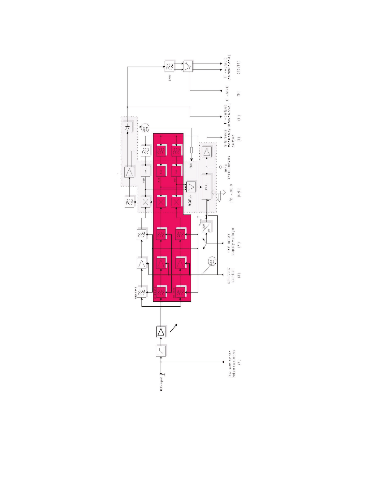
LC-32WD1E/S/RU and LC-32WT1E
[1.2] Detailed ICs Information
[1.2.1] Tuner (TD1318AF MK3)
7 - 7
Page 64

LC-32WD1E/S/RU and LC-32WT1E
[1.2.2] 12C Switch (74LVC4066PW)
7 - 8
Page 65

LC-32WD1E/S/RU and LC-32WT1E
[1.2.3] UOC Processor (TDA15134E)
7 - 9
Page 66

LC-32WD1E/S/RU and LC-32WT1E
[1.2.4] DRAM Memory (K4S161622H-UC7)
[1.2.5] EEPROM (M24C32-WMN6)
7 - 10
Page 67

LC-32WD1E/S/RU and LC-32WT1E
[1.2.6] PNX Processor (PNX5010E)
7 - 11
Page 68

LC-32WD1E/S/RU and LC-32WT1E
[1.2.7] DDR Memory (K4H561638F-UCC)
7 - 12
Page 69

LC-32WD1E/S/RU and LC-32WT1E
[1.2.8] Flash Memory (KFG5616U1A-PIB)
[1.2.9] CPLD (XC2C128-7TQG14)
7 - 13
Page 70

LC-32WD1E/S/RU and LC-32WT1E
[1.2.10] HDMI Receiver (TDA9975AEL/10)
7 - 14
Page 71

LC-32WD1E/S/RU and LC-32WT1E
[1.2.11] LVDS IC (DS90C385AMT)
[1.2.12] Video Switch (TDA8601T/C2)
7 - 15
Page 72

LC-32WD1E/S/RU and LC-32WT1E
[1.2.13] Amtel Processor (ATTINY2313V-10)
7 - 16
Page 73

LC-32WD1E/S/RU and LC-32WT1E
[1.2.14] Class D AMP (TDA8932T)
[1.2.15] Audio Switch (TEA6422D)
7 - 17
Page 74

LC-32WD1E/S/RU and LC-32WT1E
[1.2.16] Headphone AMP (TDA1308T)
[1.2.17] Voltage Regulator (LD1117DT33)
7 - 18
Page 75
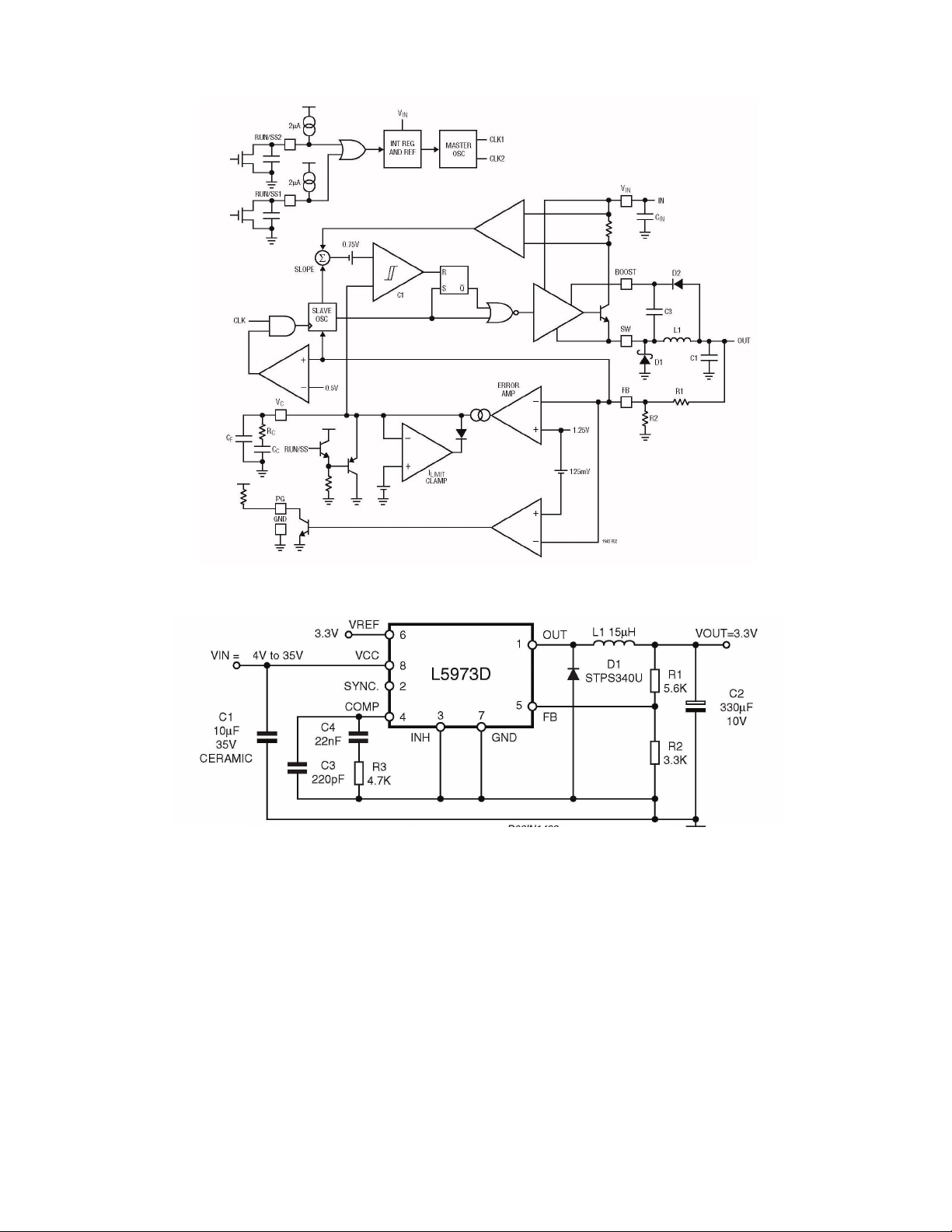
LC-32WD1E/S/RU and LC-32WT1E
[1.2.18] DC/DC Converter (LT1940EFE)
[1.2.19] Step Down Regulator (L5973D)
7 - 19
Page 76

LC-32WD1E/S/RU and LC-32WT1E
[1.2.20] Voltage Regulator (LD1117DT50)
[1.2.21] Voltage Regulator (MC34063A)
[1.2.22] Power Switch (ST890CDR)
7 - 20
Page 77
LC-32WD1E/S/RU and LC-32WT1E
[1.2.23] Voltage Regulator (MC78L08ABDR2G)
[1.2.24] Demodulator (STv0362)
7 - 21
Page 78
LC-32WD1E/S/RU and LC-32WT1E
[1.2.25] DTV Processor (STx5105)
7 - 22
Page 79

LC-32WD1E/S/RU and LC-32WT1E
[1.2.26] DDR-RAM (K4H561638F-UCC)
7 - 23
Page 80

LC-32WD1E/S/RU and LC-32WT1E
[1.2.27] Flash Memory (M29W160ET90N6)
[1.2.28] Video Filler (FMS6145MTC14)
7 - 24
Page 81
LC-32WD1E/S/RU and LC-32WT1E
[1.2.29] Buffer (74LVC245APW)
7 - 25
Page 82

LC-32WD1E/S/RU and LC-32WT1E
[1.2.30] Multiplexor (74LVC157APW)
[1.2.31] Buffer (74LVC244APW)
7 - 26
Page 83

LC-32WD1E/S/RU and LC-32WT1E
[1.2.32] DC/DC Converter (L6926)
[1.2.33] Voltage Regulator (ST1L04PT)
[1.2.34] Switching Regulator (L5973D)
7 - 27
Page 84

LC-32WD1E/S/RU and LC-32WT1E
CHAPTER 8. OVERALL WIRING DIAGRAM
[1] OVERALL WIRING DIAGRAM (LC-32WD1E/S/RU, LC-32WT1E)
12
CN7501
B14B-PASK-1
CBL000388A
X520
B14B-PH-K-S
BM V 2B M7.92 VA BK
X002
2
CBL000387
via PCB
Internal connected
X400
B8B-PH-K-S
X300
B4B-PH-K-S
X200
B10B-PH-K-S
CN2
7
X061
FI-X30SSL-HF
CN1 (LVDS)
9
8
3
0
0
0
L
B
C
0-1453230-3
SM07B-GHS-TB
S7B-PH-K-S
8
CBL000380
X0911
X060
B8B-PASK-1
CN7502
4
X062
1
9
3
0
0
0
L
B
C
0
27
9
3
0
0
0
L
B
C
S5B-PH-K-S
EXT7
S8B-PH-K-S
EXT5 EXT6
L/R
OUT
EXT4
EXT2
TVCI-SLOT
X011
EXT1
CBL000379
X0910
S4B-PH-K-S
9 4
X090
S10B-PH-K-S
CBL000378
Common wires for 32", 37" and
CBL000385
X022
S3B EH
2 2
X021
S13B-PH-K-S
S2B EH
X0208
CBL000384
12
CBL000381
EXT3
Video-Y/C
Video-CVBS
X014
S12B-PH-K-S
Audio L
Audio-R
Fast on connections
length
and 37"
42" LCD-TV, except for the
Dedicated wires for 32"
S2B-PH-K-S
X012
2
X011
S2B-PH-K-S
Headphone
2
8
3
0
0
0
L
B
C
RS-232
S9B-PH-K-S
X013
8
3
8
3
0
0
0
L
B
C
X011
OPC
Sleep
S9B-PH-K-S
Power/
OPC
IR
LED
LED
remote LED
sensor
sensor
8 - 1
Page 85

LC-32WD1E/S/RU and LC-32WT1E
[2] BLOCK DIAGRAMS
[2.1] Video
24 bit RGB
Tx
LVDS
68 MHz
CLK
~640 MHz LVDS
PLL
delay
LCD
14MHz Xtal
panel
SS PLL
control
GPIO
brightness
5V
analog (~DC)
Xtal
27MHz
27MHz_spsp
27MHz_clean
27MHz
(with or without SpSp)
DDR FLASH
133 MHz
DVBT-CVBS
DVBT-YPbPr
STB6435
STx5105
DEMOD
DVBT-audio
LM833
(3D comb filter)
LVDS_TR_EN
Filter
ext Luma
LVDS_power_EN
VIP
FGPI
YPbPr
CPLD
20bit 601 YPbPr
27 MHz
CLKout
24 bit RGB 4:4:4
27 MHz (PWM)
PWM
CLK1
27 MHz
10 bit 656 YPbPr
RGB 4:4:4
CLK2
xx MHz
CLK
/2
0
0
13,5 MHz
DDR FLASHDDR
PNX1500
200 MHz (alleen tijdens de boot)
Filter
ext Chroma
Xtal
24,576 MHz
656
MCLK
panel_error
UOC
SDRAM
audio-IF
SAW
video-IF
SAW
SAW_SW
CVBS,Y/C,L/R
Headphone L/R out
SidePCB
CVBS
CVBS,YC
SCART1
RGB or YPbPr
L/R
RGB,FB
SLCT_RGB_YPbPr
CVBS
CVBS,YC
RGB or DVBT-YPbPr
L/R
RGB,FB
SCART2
DVBT-YPbPr
DVBT-CVBS
~ 81 MS/s (9975/8)
HD: 720p & 1080i
SD: 480i/p, 576i/p
YPbPr
~ 100 MS/s (9975/10)
L/R
max 1366x768@60Hz
VGA
HIRATE
L/R
EDID
(TDA9975)
max 1080i
L/R
<300 MHz LVDS
EDID
EDID
HDMI2
max 1080i
<300 MHz LVDS
HDMI1
1) VIDEO
8 - 2
Page 86

LC-32WD1E/S/RU and LC-32WT1E
[2.2] Audio
DVBT-audio
DVBT_CVBS
DVBT-YPbPr
L,R
LM833
STB6435
CLK
enhancer
PNX
audio-
delay
CPLD
L
R
STx5105
DDR FLASH
DEMOD
2) AUDIO
CLK
SD,WS
I2S
audio-IF
SAW
I2S
video-IF
SAW
Classe D 6 Watt speakers
AUDoutLS
AUDIO_IN4
L/R
Headphone L/R out
SidePCB
(brom 50/60Hz)
HP amp
AUDoutPH
AUDIO_IN3
L/R
DVBT-audio
LINE OUT
QRWVXSSRUWHG
AUDIOoutS
L/R in
L/R out
SCART1
AUDIO_IN2
AUDIOoutLR
L/R in
L/R out
SCART2
I2C
AUDIO_IN5
L,R
HIRATE
(TDA9975)
I2S
DAC
video + audio (LPCM)
L/R
L/R
YPbPr
VGA
L/R
HDMI1
EDID
EDID
EDID
HDMI2
8 - 3
Page 87

LC-32WD1E/S/RU and LC-32WT1E
[2.3] Control
SUBD9
SERVICE-CONN
RS_ATMEL
RS_ST
RS232
(development only)
I2C
Service_select
I2C switch
I2C
LEDs,
panel,
GPIO
...
PNX
X043
PNX-EEP
RX,TX
INT
TM_SCL,TM_SDA
SCL,SDA
(X011)
I2C HDR
(X010)
I2C HDR
TEMP sensor
I2C switch
UOCV_SCL,UOCV_SDA
HW I2C
SW I2C
UOC
ST-Heartbeat-LED
RX,TX2
I2C
RX/TX1
INT
(backup)
STx5105
TS
CI
CI slot
module
I2C
RX/TX
CPU
ATMEL
GPIO
INT[2]
UOC EEP
A switch
I2C HDR
CPLD
HIRATE
(TDA9975)
Mode[3]
ARX
I2C
BRX
I2C
EEPROM
DEMOD
I2C
I2C
AGC
KEYB
KEYB pcb
OPC, REMOTE
4x LED
LED/IR pcb
VGA
I2C
EDID
EDID
HDMI1
I2C
EDID
HDMI2
I2C
3) CONTROL
8 - 4
Page 88

LC-32WD1E/S/RU and LC-32WT1E
[2.4] Memories
X048
SUBD9
SERVICE-CONN
RS_ST
(development only)
option for service:
RS232
update PNX-EEP,
RS_ATMEL
UOC-FLASH,
PNX-FLASH
Service_select
X1401
I2C
X041
X040
JCON
20MHz
JTAG
16 MByte
OneNand FLASH
Boot-mode (from JCON or FLASH)
GPIO15
DDR,
200 MHz,
64 MByte
I2C switch
JTAG / EJTAG
I2C
WPn
PNX
JTAG
2 or 4 MB
NOR-FLASH,
DDR
32 MB, 133 MHz
FLASH
X043
PNX-EEP
RX,TX
INT
TM_SCL,TM_SDA
SCL,SDA
HW I2C
(X011)
I2C HDR
(X010)
I2C switch
I2C HDR
UOC EEP
UOCV_SCL,UOCV_SDA
SW I2C
JTAG
UOC
RAM: 8KB
FLASH: 256KB
SDRAM
DCU
JTAG
JTAG / DCU
RX/TX
ATMEL
FLASH: 2K
I2C HDR
I2C
RAM: 128B
EEPROM: 128B
EEPROM
STx5105
TS
RX,TX2
I2C
RX/TX1
INT
X1108
JTAG
card
CI slot
I2C HDR
INT[2]
FLASH
JTAG
JTAG
CPLD
HIRATE
(TDA9975)
Mode[3]
(3D comb filter)
DEMOD
I2C
Write-Protected
4) MEMORIES
I2C
AGC
8 - 5
VGA
I2C
(7)
EDID
EDID
HDMI1
I2C
(8)
EDID
HDMI2
I2C
(9)
Page 89

LC-32WD1E/S/RU and LC-32WT1E
[2.5] CPU and Memories
NOR-FLASH,
2 or 4 MB
STx5105
I2C
ATMEL
RAM: 128B
FLASH: 2K
EEPROM: 128B
TM_SCL,TM_SDA
SCL,SDA
I2C
16 MByte
OneNand FLASH
DDR,
200 MHz,
64 MByte
PNX
WPn
PNX-EEP
(4KB)
(4KB)
UOC EEP
INT[2]
FLASH
Mode[3]
CPLD
I2C switch
UOCV_SCL,UOCV_SDA
DDR
32 MB, 133 MHz
FLASH
card
CI slot
RX/TX1
INT
TS
I2C
EEPROM
DEMOD
I2C
5) CPUs & MEMORIES
I2C
AGC
RX,TX
INT
HW I2C
RAM: 8KB
FLASH: 256KB
UOC
SW I2C
HIRATE
(TDA9975)
SDRAM
(3D comb filter)
VGA
I2C
EDID
EDID
HDMI1
I2C
EDID
HDMI2
I2C
8 - 6
Page 90
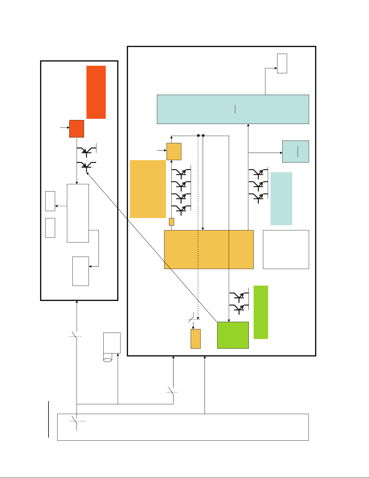
LC-32WD1E/S/RU and LC-32WT1E
[2.6] Reset
FLASH
PNX_RST_OUTN
3V3D
DDR FLASH
1) ST-reset-button (DEV)
2) Power-On-Reset-IC
3) Reset by ATMEL
POR
3V3STB
ResetOutn
1) internal POR
2) UOC-reset-button (DEV)
3) Power-On-Reset-IC
4) Power-Down-circuit
5) UOC-Self-Reset
STx5105
FE_RSTn
DEMOD
POR
6) Power-good circuit
1V8
RESETN
UOC
PNX
CPLD
1) door UOC
2) Power-Down-circuit
PNX,CPLD_resetn
3) PNX reset-button (DEV)
HIRATE
(TDA9975)
(SW-reset)
12V 12V_DIG
6) RESET
12V_DVBT_ON
psu_standby
(atmel)
(uoc)
3V3STB
same as UOC +
RESETN
UOC EEP
12V_TV_ON
3V3STB
(atmel)
U
12V_ANA
P
S
ATMEL
ATMEL-programmer
8 - 7
Page 91
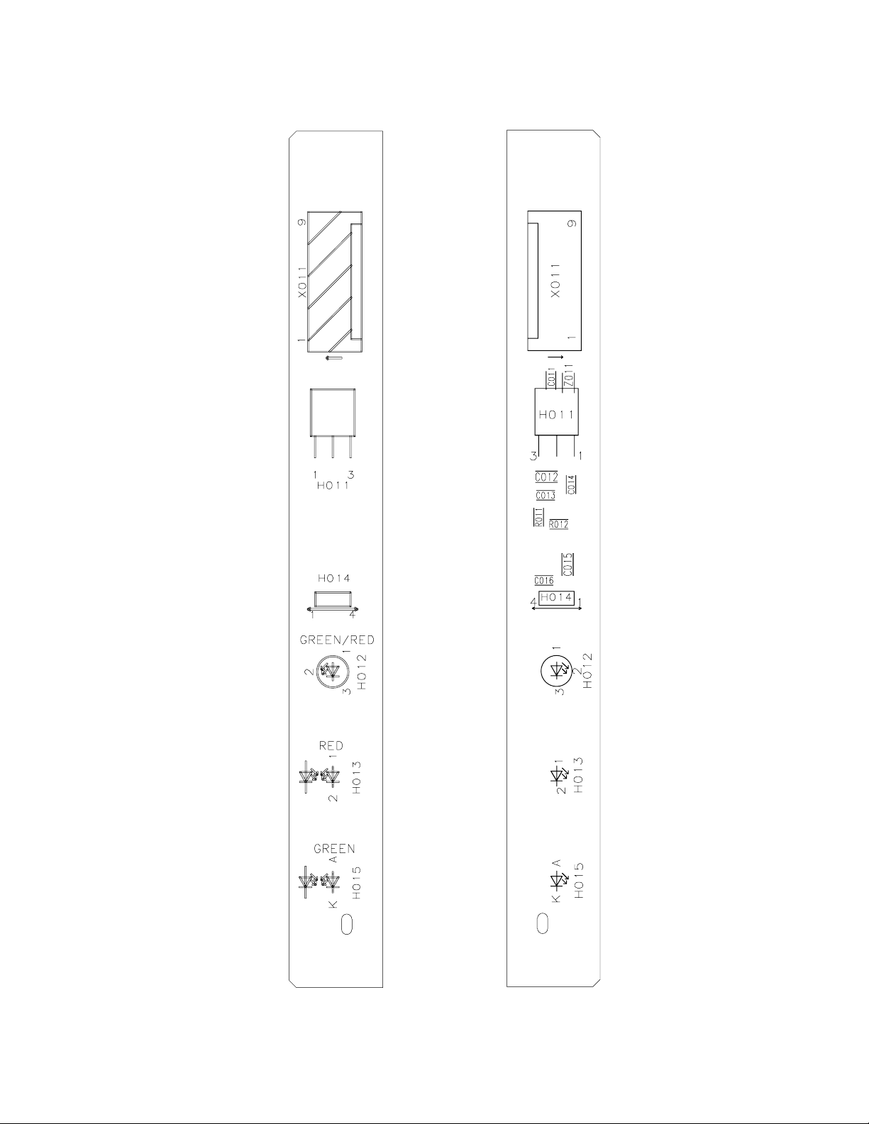
LC-32WD1E/S/RU and LC-32WT1E
CHAPTER 9. PRINTED WIRING BOARD
[1] LED/IR
9 - 1
Page 92

LC-32WD1E/S/RU and LC-32WT1E
[2] SIDE I/O
9 - 2
Page 93
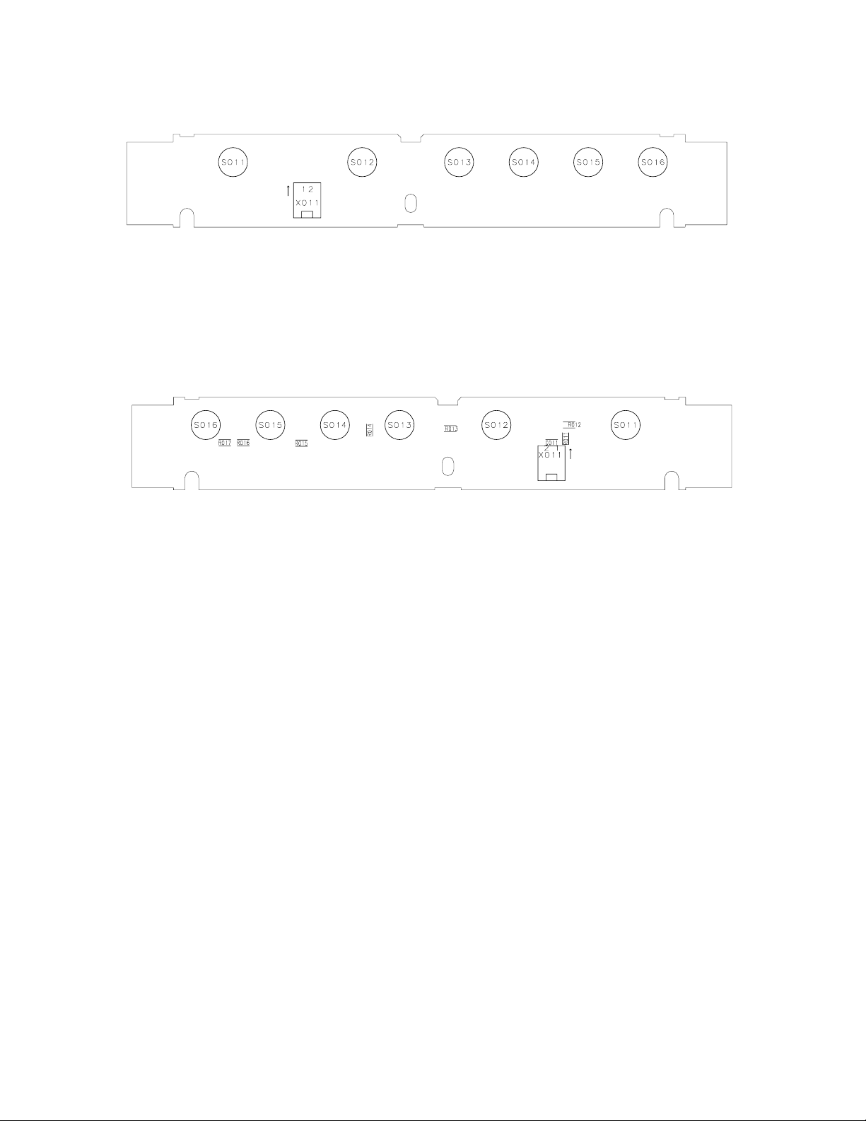
LC-32WD1E/S/RU and LC-32WT1E
[3] KEYPAD
9 - 3
Page 94
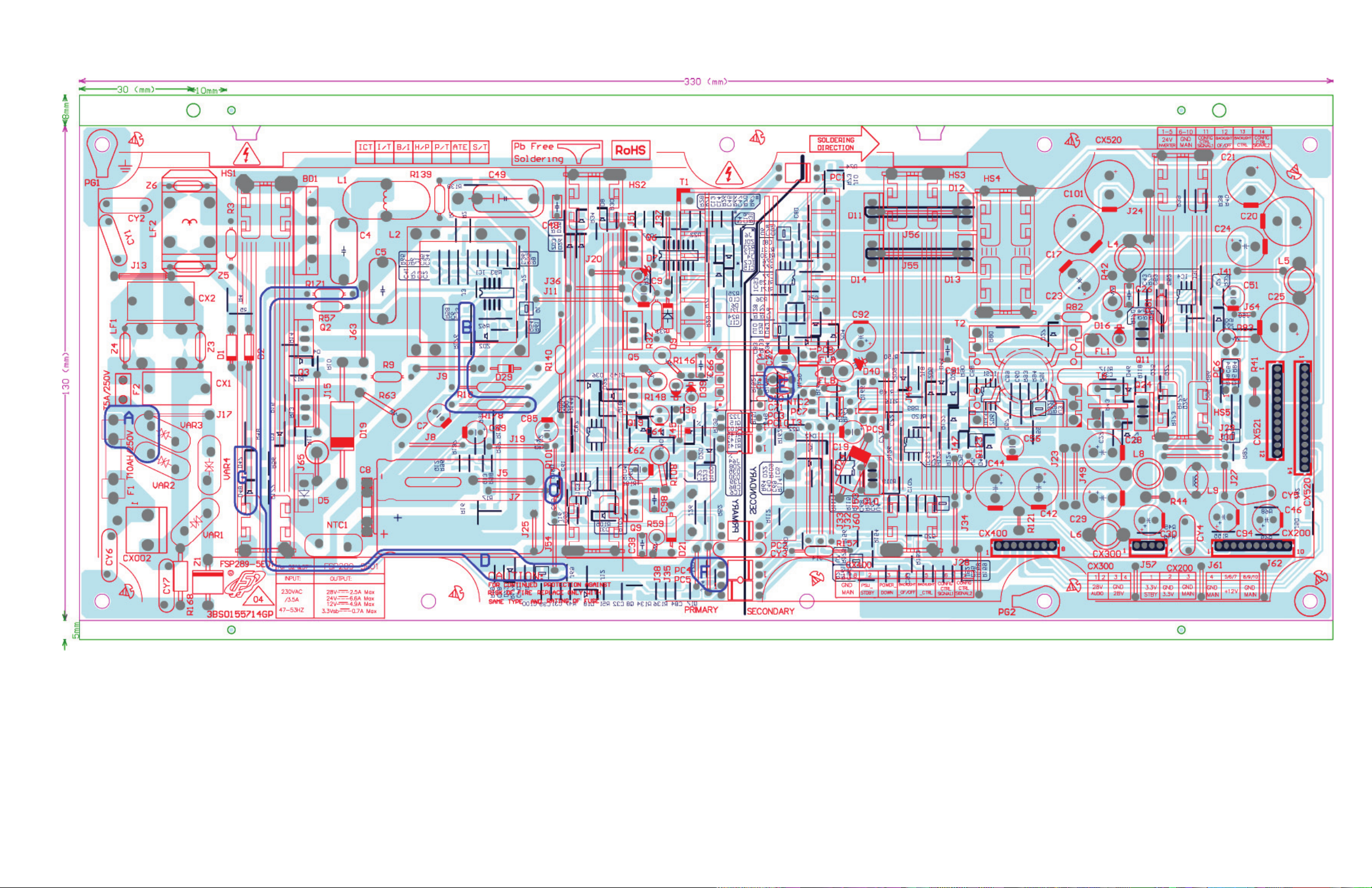
LC-32WD1E/S/RU and LC-32/37/42WT1E
[4] POWER UNIT PRINTED WIRING BOARD
For information on having this page automatically print to a larger page size, see page i.
9 - 4
Page 95
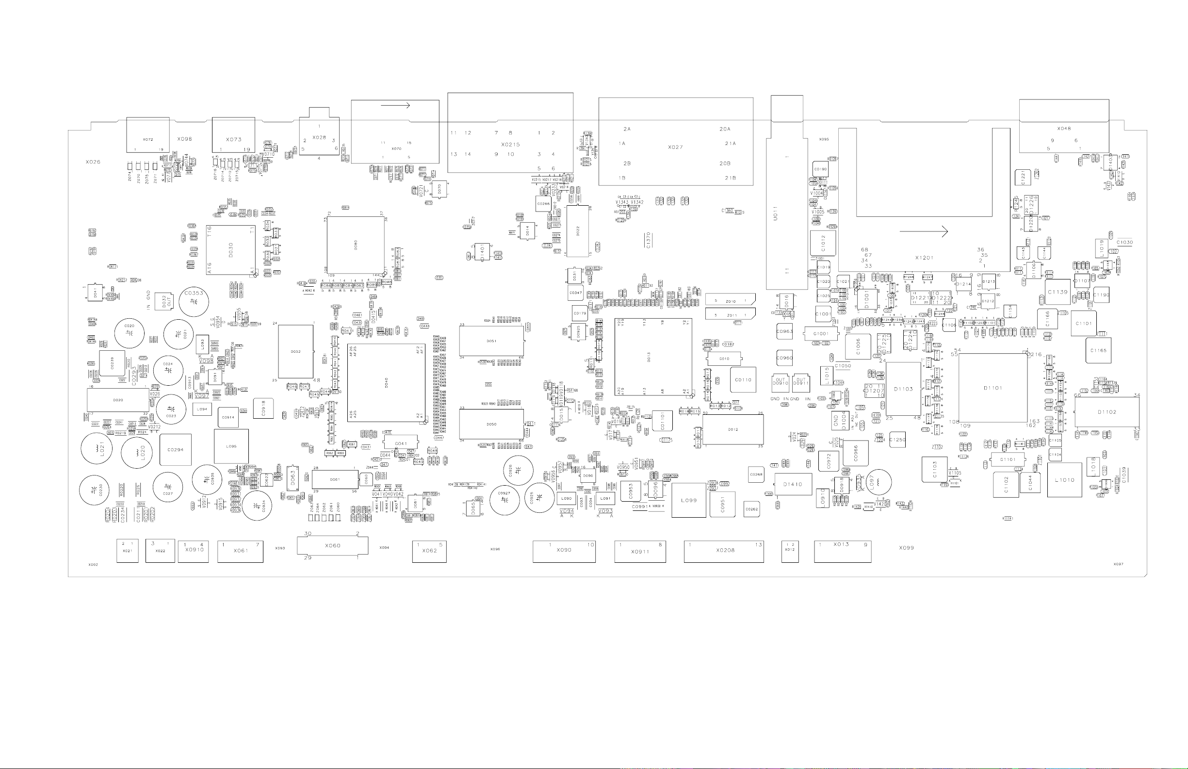
LC-32WD1E/S/RU and LC-32/37/42WT1E
[5] MAINBOARD
[5.1]Side A
For information on having this page automatically print to a larger page size, see page i.
9 - 5
Page 96

LC-32WD1E/S/RU and LC-32/37/42WT1E
[5.2]Side B
For information on having this page automatically print to a larger page size, see page i.
9 - 6
Page 97

LC-32WD1E/S/RU and LC-32WT1E
CHAPTER 10. SCHEMATIC DIAGRAM
[1] DESCRIPTION OF SCHEMATIC DIAGRAM
COMPONENT VALUE AND PARTS LIST
1. For the correct value and/or type number of components,
always refer to the parts list. Values and type number in the
schematics are for reference only.
RESISTOR
1. For resistors value the "Ω" is omitted:
100R = 100Ω, 10K = 10KΩ, 1M = 1MΩ
2. For resistor power rating and tolerance
refer to the parts list.
CAPACITOR
1. For capacitor values in the schematics
the "F" is omitted:
10p = 10pF, 10n = 10nF,10μ = 10μF
2. For capacitor voltage rating refer to
the parts list.
WARNING:
THESE CIRCUIT DIAGRAMS ARE THE ORIGINAL ONES,
THEREFORE THERE MAY BE A SLIGHT DIFFERENCE
FROM YOUR UNIT.
WARNING:
SAFETY NOTES:
1. DISCONNECT THE AC PLUG FROM THE AC
OUTLET BEFORE REPLACING PARTS.
2. SEMICONDUCTOR HEAT SINKS SHOULD BE
REGARDED AS POTENTIAL SHOCK HAZARDS
WHEN THE CHASSIS (SET) IS OPERATING.
WARNING:
IMPORTANT SAFETY NOTICE:
PARTS MARKED WITH “ ” ( ) ARE
IMPORTANT FOR MAINTAINING THE SAFETY OF THE
SET. BE SURE TO REPLACE THESE PARTS WITH
SPECIFIED ONES FOR MAINTAINING THE SAFETY AND
PERFORMANCE OF THE SET.
10 - 1
Page 98

LC-32WD1E/S/RU and LC-32WT1E
[1] LED/IR
C016
100n
3
+3V3
4
H014
TPS855
S9B-PH-K-S
9
8
7
6
5
4
3
2
1
X011
TP016
TP013
TP014
TP015
TP017
TP012
TP018
TP019
Z011
BLM21PG221SN1D
+3V3
C011
470n
C015
10u
+3V3
R011
C012
100R
4u7
C013
100n
R012
C014
1K
68p
GREEN
H012-2
32
L-115WEGW
H012-1
RED
1
L-115WEGW
NC
1
3
1
2
TSOP34838SB1
2
2
H011
VS
OUT
GND
10 - 2
H013
204-10SURT/S530-A3
H015
204-10SYGT/S530-E3
Page 99

LC-32WD1E/S/RU and LC-32WT1E
[2] SIDE I/O
R014
4R7
4R7
R015
100p
C012
100p
C011
R013
150R
R012
150R
1
2345678
X014
10
11
12
9
S12B-PH-K-S
150R
R016
100p
C017
100p
C016
R018
220R
R019
220R
100p
C015
100p
C014
0RR0110
0R
R0111
6
123
X011-1
MSP-866H-BAB-01 NIFE
BZX284-C15
BZX284-C15
V0114
BZX284-C15
V0112
BZX284-C15
R011
0R
V019
V017
V015
3
V011
12
PESD5V0S2BT
4
7
12
13
5
X011-2
YELLOW
10911
WHITE
X011-3
MSP-866H-BAB-01 NIFE
MSP-866H-BAB-01 NIFE
8
RED
X011-4
MSP-866H-BAB-01 NIFE
V0110
BZX284-C15
BZX284-C15
V018
BZX284-C15
BZX284-C15
V016
BZX284-C15BZX284-C15
19
20
1415161718
X011-5
V0113
V0111
MSP-866H-BAB-01 NIFE
10 - 3
Page 100
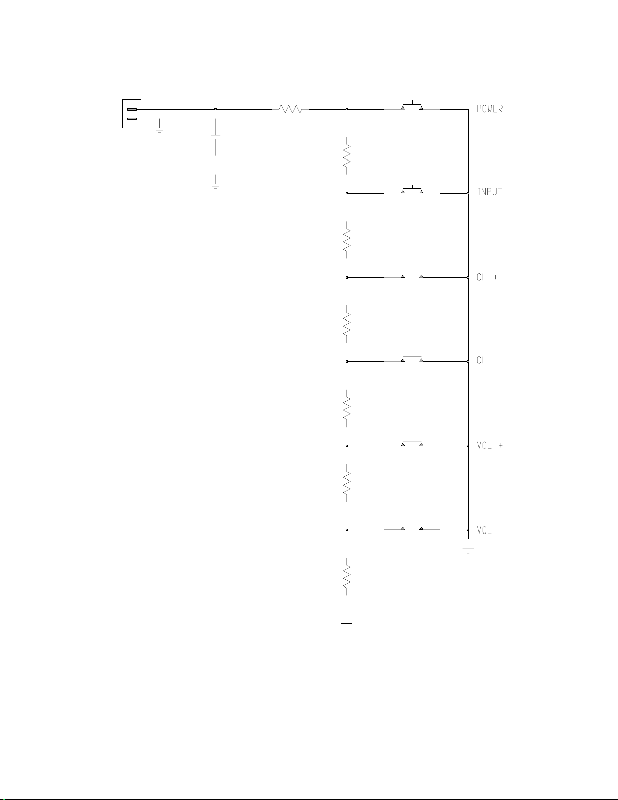
LC-32WD1E/S/RU and LC-32WT1E
[3] KEYBOARD
X011
1
2
S2B-PH-K-S
C011
68p
R011
47R
R012
R013
R014
S011
EVQ11L05R
100R
S012
EVQ11L05R
124R
S013
EVQ11L05R
300R3K3
S014
EVQ11L05R
R015
R016
R017
510R
S015
EVQ11L05R
1K47
S016
EVQ11L05R
10 - 4
 Loading...