

Page 1
LC-32SV502B/LC-42SV502B/LC-42SV602B/LC-46SV602B/LC-46SV502L
[2]
SHARP
SERVICE MANUAL
LCD COLOUR TELEVISION
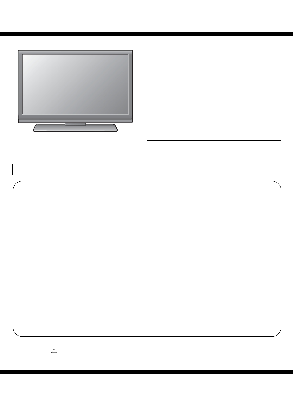
LC-32SV502B
LC-42SV502B
LC-42SV602B
LC-46SV602B
MODEL LC-46SV502L
In the interests of user-safety (Required by safety regulations in some countries) the set should be restored to its original condition and only parts identical to those specified should be used.
SAFETY PRECAUTION
IMPORTANT SERVICE SAFETY PRECAUTION ..................2
PRECAUTIONS FOR USING LEAD-FREE SOLDER ...........3
CHAPTER 1. OPERATION MANUAL
[1] SPECIFICATIONS ............................................................4
[2] OPERATION MANUAL .....................................................7
[3] DIMENSIONS .................................................................16
CHAPTER 2. REMOVING OF MAJOR PARTS
[1] ASSY/PANEL REMOVAL................................................18
[2] SET RE-ASSEMBLY.......................................................28
CHAPTER 3. ADJUSTMENT PROCEDURE
[1] ADJUSTMENT PROCEDURE ........................................29
[2] SOFTWARE UPGRADE PRODUCE ..............................34
CHAPTER 4. TROUBLESHOOTING TABLE
[1] TROUBLESHOOTING TABLE .......................................40
CHAPTER 5. MAJOR IC INFORMATIONS
[1] MAJOR IC INFORMATION .............................................46
DETAIL ICs INFORMATION ...........................................56
Parts marked with " " are important for maintaining the safety of the set. Be sure to replace these parts with specified ones for maintaining the
safety and performance of the set.
SHARP CORPORATION
CONTENTS
CHAPTER 6. BLOCK DIAGRAM/WIRING DIAGRAM
[1] BLOCK DIAGRAM ..........................................................67
[2] WIRIGN DIAGRAM ……..................................................68
CHAPTER 7. PRINTED WIRING BOARD
[1] MAIN UNIT PRINTED WIRING BOARD …..……............70
[2] POWER UNIT PRINTED WIRING BOARD ....................72
[3] KEY UNIT PRINTED WIRINGBOARD ............................76
[4] IR UNIT PRINTED WIRING BOARD ..............................76
CHAPTER 8. SCHEMATIC DIAGRAM
[1] MAIN SCHEMATIC DIGRAM .........................................77
[2] POWER SCHEMATIC DIGRAM .....................................92
[3] KEY SCHEMATIC DIGRAM …………….........................99
[4] IR SCHEMATIC DIGRAM ..........................
CHAPTER 9. PARTS GAUILD
[1] SPARE PARTS LIST .........................
[2] CABINET PARTS .........................................
[3] PACKING PARTS ………………………………………138
...................100
...........................101
...............134
This document has been published to be used for
after sales service only.
The contents are subject to change without notice.
1
Page 2
LC-32SV502B/LC-42SV502B/LC-42SV602B/LC-46SV602B/LC-46SV502L
SAFETY PRECAUTION
IMPORTANT SERVICE SAFETY PRECAUTION
■ Service work should be performed only by qualified service technicians who are thoroughly familiar with all safety checks and the
servicing guidelines which follow:
■ WARNING
1. For continued safety, no modification of any circuit should be
attempted.
2. Disconnect AC power before servicing.
CAUTION:
FOR CONTINUED PROTECTION AGAINST A
RISK OF FIRE REPLACE ONLY WITH SAME
TYPE FUSE.
F9901/F9902 (6.3A/250V)
■
BEFORE RETURNING THE RECEIVER
(Fire & Shock Hazard)
Before returning the receiver to the user, perform the following
safety checks:
3. Inspect all lead dress to make certain that leads are not pinched,
and check that hardware is not lodged between the chassis and
other metal parts in the receiver.
4. Inspect all protective devices such as non-metallic control knobs,
insulation materials, cabinet backs, adjustment and compartment
covers or shields, isolation resistor-capacitor networks, mechanical
insulators, etc.
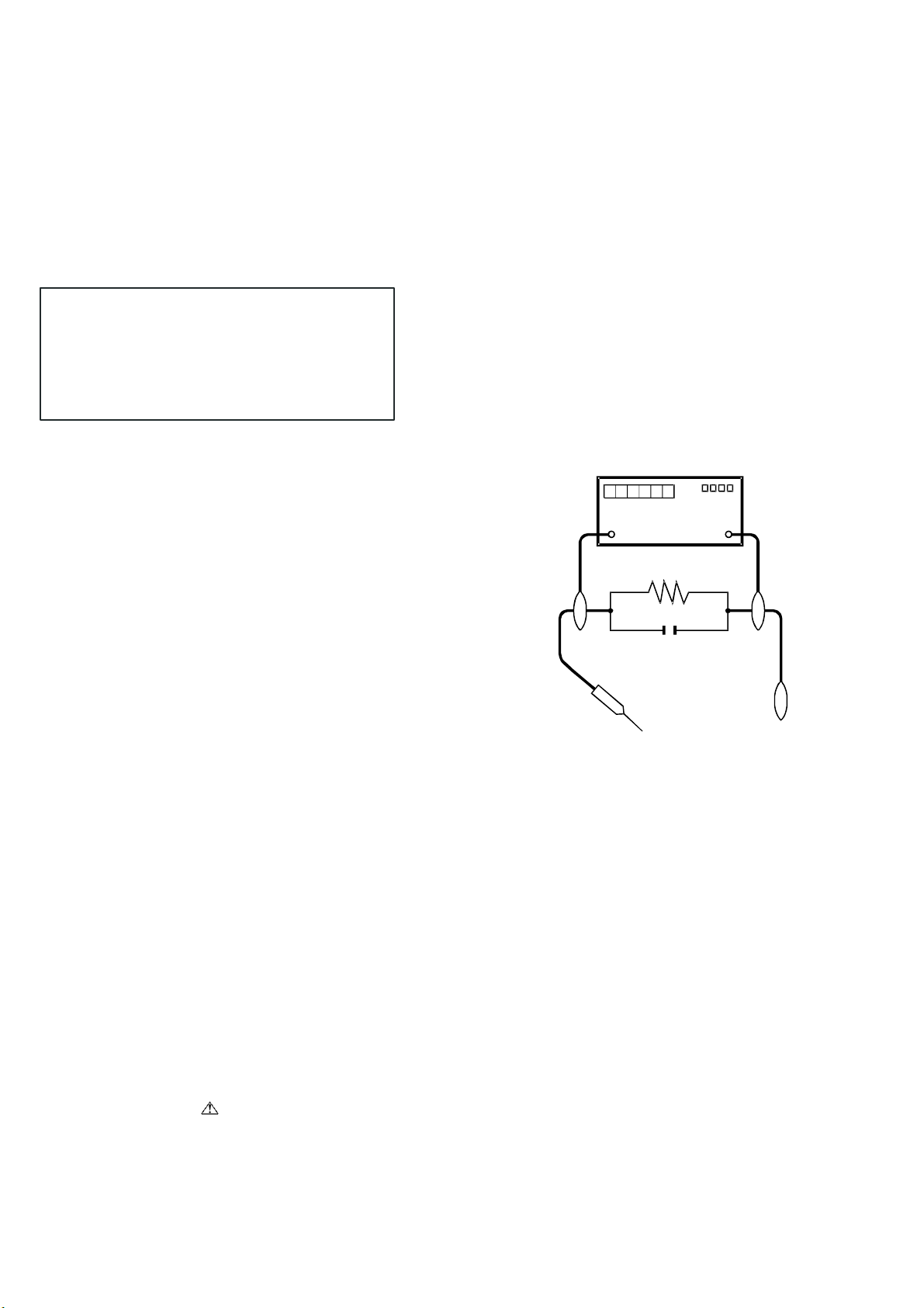
5. To be sure that no shock hazard exists, check for leakage current in
the following manner.
• Plug the AC cord directly into a 220~240 volt AC outlet.
• Using two clip leads, connect a 1.5k ohm, 10 watt resistor paralleled
by a 0.15µF capacitor in series with all exposed metal cabinet
parts and a known earth ground, such as electrical conduit or
electrical ground connected to an earth ground.
//////////////////////////////////////////////////////////////////////////////////////////////////////////////////////////////////////////////////////////////////////////////////////////////////////////////////////////////////////////////////
SAFETY NOTICE
Many electrical and mechanical parts in LCD color television have
special safety-related characteristics.
These characteristics are often not evident from visual inspection,
nor.
can protection afforded by them be necessarily increased by using
replacement components rated for higher voltage, wattage, etc.
Replacement parts which have these special safety characteristics
are identified in this manual; electrical components having such
features are identified by “
Replacement Parts List and Schematic Diagrams.
//////////////////////////////////////////////////////////////////////////////////////////////////////////////////////////////////////////////////////////////////////////////////////////////////////////////////////////////////////////////////
” and shaded areas in the
• Use an AC voltmeter having with 5000 ohm per volt, or higher, sen-
sitivity or measure the AC voltage drop across the resistor.
• Connect the resistor connection to all exposed metal parts having a
return to the chassis (antenna, metal cabinet, screw heads, knobs
and control shafts, escutcheon, etc.) and measure the AC voltage
drop across the resistor.
All checks must be repeated with the AC cord plug connection
reversed. (If necessary, a nonpolarized adaptor plug must be used
only for the purpose of completing these checks.)
Any reading of 1.05 V peak (this corresponds to 0.7 mA peak AC.)
or more is excessive and indicates a potential shock hazard which
must be corrected before returning the monitor to the owner.
DVM
AC SCALE
1.5k ohm
10W
0.15 µF
TEST PROBE
TO EXPOSED
METAL PARTS
CONNECT TO KNOWN
EARTH GROUND
For continued protection, replacement parts must be identical to those
used in the original circuit.
The use of a substitute replacement parts which do not have the same
safety characteristics as the factory recommended replacement parts
shown in this service manual, may create shock, fire or other hazards.
2
Page 3

LC-32SV502B/LC-42SV502B/LC-42SV602B/LC-46SV602B/LC-46SV502L
PRECAUTIONS FOR USING LEAD-FREE SOLDER
■ Using lead-free wire solder
• When fixing the PWB soldered with the lead-free solder, apply lead-free wire solder. Repairing with conventional lead wire solder may cause damage
or accident due to cracks.
As the melting point of lead-free solder (Sn-Ag-Cu) is higher than the lead wire solder by 40 °C, we recommend you to use a dedicated soldering bit, if
you are not familiar with how to obtain lead-free wire solder or soldering bit, contact our service station or service branch in your area.
Soldering
• As the melting point of lead-free solder (Sn-Ag-Cu) is about 220 °C which is higher than the conventional lead solder by 40 °C, and as it has poor
solder wettability, you may be apt to keep the soldering bit in contact with the PWB for extended period of time. However, Since the land may be
peeled off or the maximum heat-resistance temperature of parts may be exceeded, remove the bit from the PWB as soon as you confirm the steady
soldering condition.
Lead-free solder contains more tin, and the end of the soldering bit may be easily corroded. Make sure to turn on and off the power of the bit as
required.
If a different type of solder stays on the tip of the soldering bit, it is alloyed with lead-free solder. Clean the bit after every use of it.
When the tip of the soldering bit is blackened during use, file it with steel wool or fine sandpaper.
• Be careful when replacing parts with polarity indication on the PWB silk.
3
Page 4
LC-32SV502B/LC-42SV502B/LC-42SV602B/LC-46SV602B/LC-46SV502L
CHAPTER 1. OPERATION MANUAL
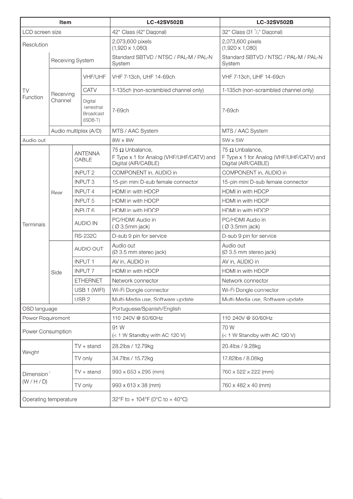
[1] SPECIFICATIONS
Item LC-46SV502L
LCD screen size 46" Class (46" Diagonal)
Resolution 2,073,600 pixels (1,920 x 1,080)
Receiving System Standard SBTVD /NTSC System
VHF/UHF VHF 2-13ch, UHF 14-69ch
TV Function
Audio out 8W x 8W
Terminals
Receiving Channel
Audio multiplex (A/D) MTS / AAC System
Rear
Side
CATV 1-135ch (non-scrambled channel only)
Digital Terrestrial Broadcast (ISDB-T) 2-69ch
ANTENNA
CABLE
INPUT 2 COMPONENT in, AUDIO in
INPUT 3 15-pin mini D-sub female connector
INPUT 4 HDMI in with HDCP
INPUT 5 HDMI in with HDCP
INPUT 6 HDMI in with HDCP
AUDIO IN
RS-232C D-sub 9 pin for service & Hotel mode using
AUDIO OUT Audio out (Ø 3.5 mm stereo jack)
INPUT 1 AV in, AUDIO in
INPUT 7 HDMI in with HDCP
75 qUnbalance,
F Type x 1 for Analog (VHF/UHF/CATV) and Digital (AIR/CABLE)
PC/HDMI Audio in
( Ø 3.5mm jack)
USB 1 Multi-Media use, Software update
USB 2 Multi-Media use, Software update
OSD language English/Portuguese/Spanish
Power Requirement 110-240V @ 50/60Hz
Power Consumption 127 W(< 1 W Standby with AC 120 V)
TV + stand 39.9 lbs / 18.11 kg
Weight
TV only 33.5 lbs / 15.18 kg
Dimension*1
(W / H / D)
Operating temperature 32°F to + 104°F (0°C to + 40°C)
TV + stand 1,081 x 702 x 295 (inch)
TV only 1,081 x 662 x 38 (inch)
4
Page 5
LC-32SV502B/LC-42SV502B/LC-42SV602B/LC-46SV602B/LC-46SV502L
5
Page 6
LC-32SV502B/LC-42SV502B/LC-42SV602B/LC-46SV602B/LC-46SV502L
*1 The dimensional drawings are shown on the inside back cover.
• As a part of policy of continuous improvement, SHARP reserves the right to make design and specification changes for product improvement without
prior notice. The performance specification figures indicated are nominal values of production units. There may be some deviations from these values in
individual units.
6
Page 7
[2] OPERATION MANUAL
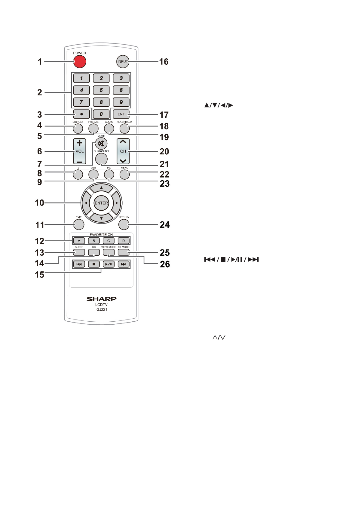
Remote Control (LC-46SV502L)
NOTE
• When using the remote control unit, point it at the TV.
1 POWER: Switch the power on or enter standby mode.
2 0–9: Set the channel.
3 • (DOT)
4 DISPLAY: Display the current channel (or input source)
information on the screen.
LC-32SV502B/LC-42SV502B/LC-42SV602B/LC-46SV602B/LC-46SV502L
5 FREEZE: Set the still image. Press again to return to
normal screen.
6 VOL +/-: Set the volume.
7 MUTE: Mute the sound.
8 TV: Switch to TV input source.
9 USB: Switch to USB input source.
10
screen.
11 EXIT: Turn off the menu screen.
12 FAVORITE CH: A, B, C, D: Select 4 preset favorite
channels in 4 different categories. While watching, you
can toggle the selected channels by pressing A, B, C and
D.
13 SLEEP: Allows you to set a time when the TV
automatically switches to standby. This display will
disappear after few seconds, and the sleep timer starts to
count down automatically.
• If you want to adjust the sleep timer again, you can press
this button repeatedly then change the time setting.
• The TV will enter into the standby mode when the
remaining time reaches zero.
14 CC: Display captions during closed-caption source.
15
16 INPUT: Select a TV input source.
17 ENT: Jumps to a channel after selecting with the 0–9
buttons.
18 FLASHBACK: Press to switch to the previously tuned
channel. Press again to switch back to the currently tuned
channel.
19 AUDIO: Display the MTS/SAP setting menu.
20 CH
21 SURROUND: Display the surround setting menu.
22 MENU: Display the menu screen.
23 PC: Switch to PC input source.
24 RETURN: Return to the previous menu screen.
25 AV MODE: Select an adjusted picture settings.
(Standard, Movie, Power Saver, User, Dynamic)
26 VIEW MODE: Select the Picture Mode.
ENTER: Select a desired item on the
: Select the channel.
7
Page 8
LC-32SV502B/LC-42SV502B/LC-42SV602B/LC-46SV602B/LC-46SV502L
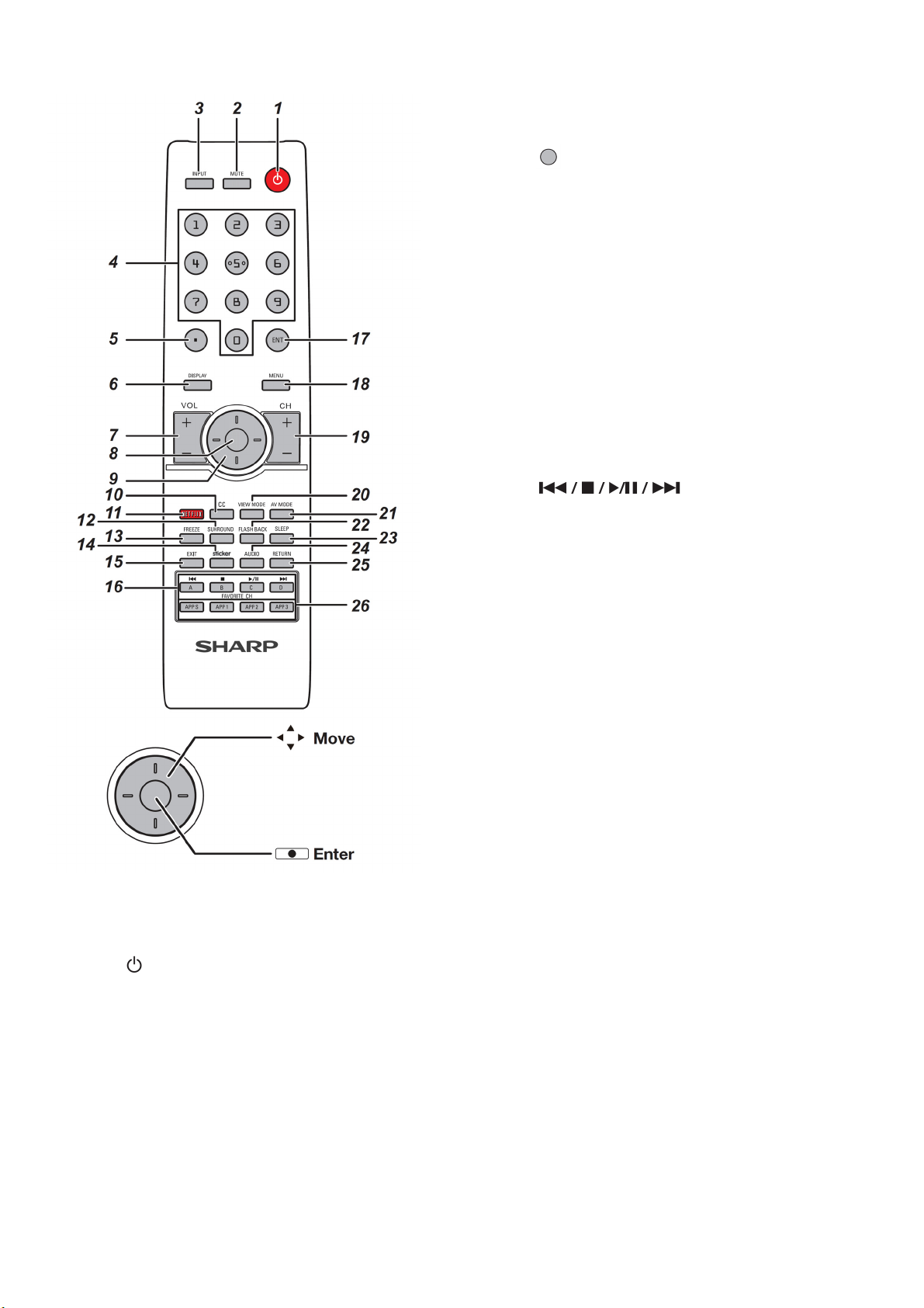
Remote Control (LC-32SV502B/LC-42SV502B/LC-42SV602B/LC-46SV602B)
7 VOL +/-:
8
9 Navigation buttons:
10 CC:
11 NETFLIX:
12 SURROUND:
13 FREEZE:
normal screen.
14 Sticker:
15 EXIT:
16 FAVORITE CH:
A, B, C, D : Select 4 preset favorite channels in 4 different
categories. While watching, you can toggle the selected
channels by pressing A, B, C and D.
17 ENT:
buttons.
18 MENU:
19 CH +/
20 VIEW MODE :
21 AV MODE:
Movie, Power Saver, User, Dynamic
22 FLASHBACK:
Channel . Press again to switch back to the currently
tuned channel.
23 SLEEP:
switches to standby. This display will disappear after few
seconds , and the sleep timer starts to count down
automatically .
• If you want to adjust the sleep timer again, you can press
NOTE
• When using the remote control unit, point it at the TV.
1
(Power): Switch the power on or enter standby
mode.
2 MUTE: Mute the sound.
3 INPUT: Select a TV input source.
• The TV will enter into the standby mode when the
24 AUDIO:
25 RETURN:
26 APP S / APP 1 / APP 2 / APP 3:
favorite applications to these buttons.
Set the volume.
(Enter):
this button repeatedly then change the time setting.
remaining time reaches zero.
Confirm a selected item.
Select a desired item on the screen.
Display captions during closed-caption source.
Enable NETFLIX function.
Display the surround setting menu.
Set the still image. Press again to return to
No function.
Turn off the menu screen.
Jumps to a channel after selecting with the 0–9
Display the menu screen.
- : Select the channel.
Select the Picture Mode.
Select an adjusted picture settings. (
)
Press to switch to the previously tuned
Allows you to set a time when the TV automatically
Display the MTS/SAP setting menu.
Return to the previous menu screen.
You can assign your
Standard
,
4 0–9: Set the channel.
5 • (DOT)
6 DISPLAY: Display the current channel (or input source)
information on the screen.
8
Page 9
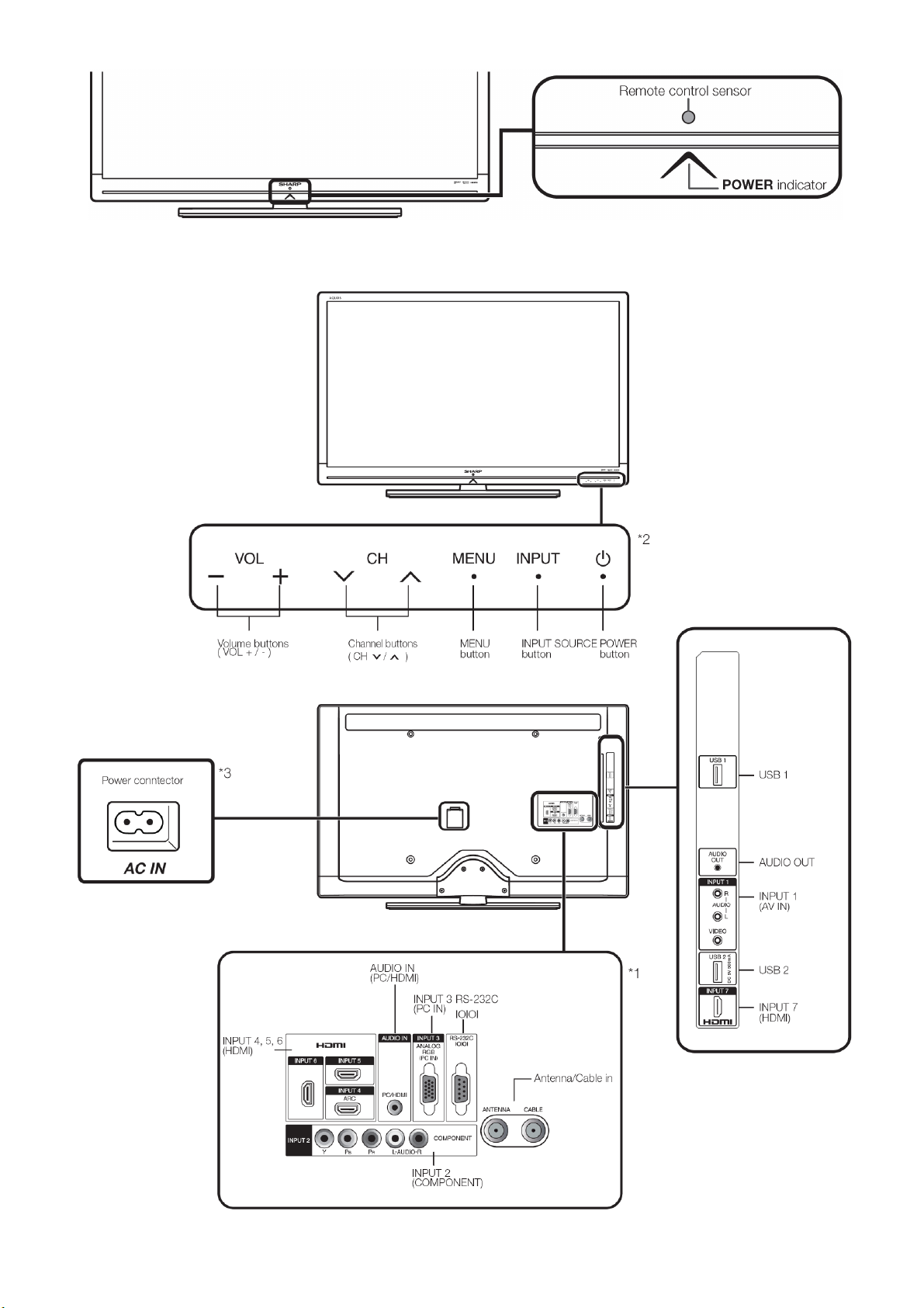
TV (Front)
TV (Side/Rear)
LC-32SV502B/LC-42SV502B/LC-42SV602B/LC-46SV602B/LC-46SV502L
NOTE
• The illustrations in this operation manual are for explanation purposes and may vary slightly from the actual operations.
9
Page 10
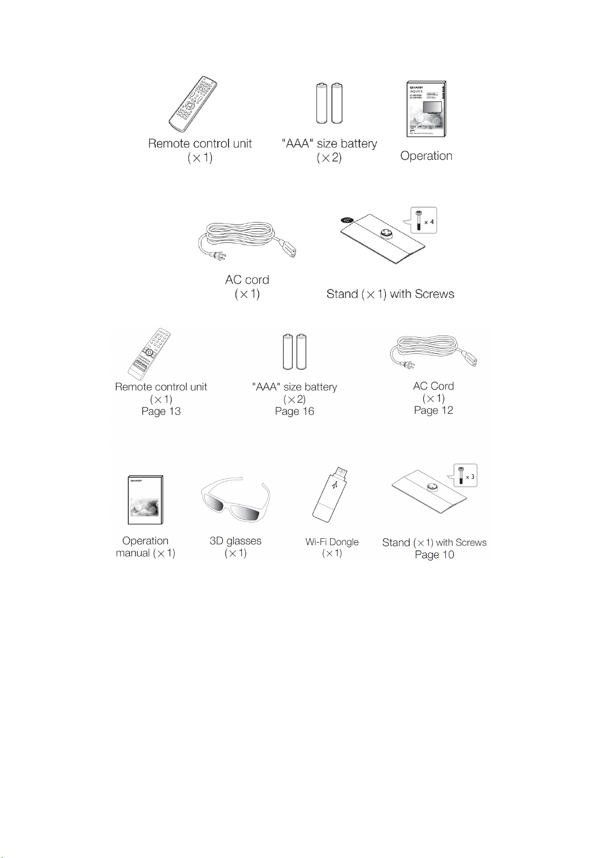
LC-32SV502B/LC-42SV502B/LC-42SV602B/LC-46SV602B/LC-46SV502L
Preparation
Supplied Accessories
LC-46SV502L
LC-32SV502B/LC-42SV502B/LC-42SV602B/LC-46SV602B
Note
• Always use the AC cord supplied with the TV.
• The illustrations above are for explanation purposes and may vary slightly from the actual accessories
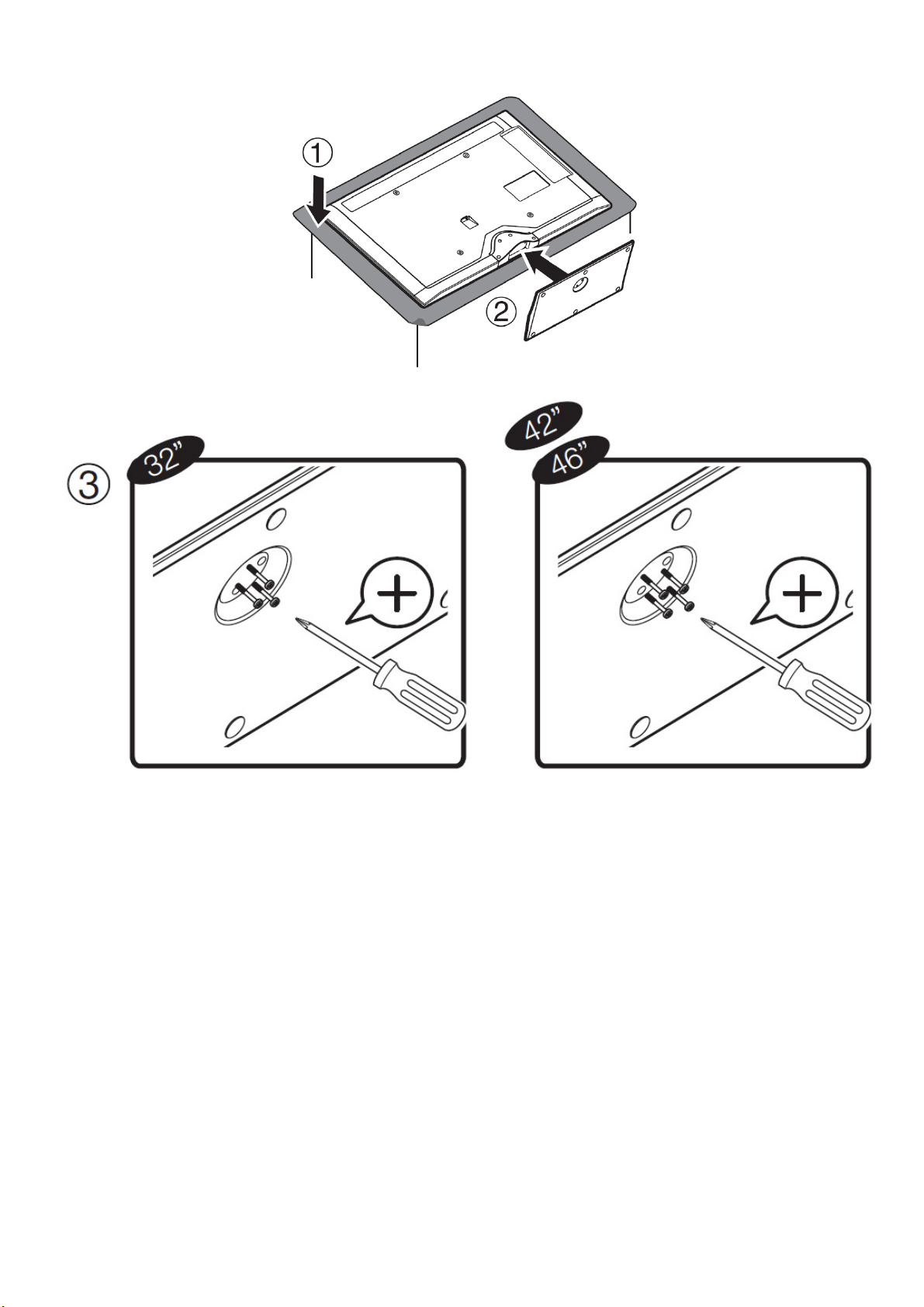
Attaching/Detaching the Stand
• Before attaching (or detaching) the stand, unplug the AC cord from the AC IN terminal.
• Before attaching (or detaching) the stand, spread a cushion under the TV to prevent it from being damaged.
Caution
• Attach the stand in the correct direction.
• Be sure to follow the instructions.Incorrect installation of the stand may result in the TV falling over.
1 Put the TV face down on a safe surface that is covered by a soft and smooth cloth.
2 Adjust the TV stand to the bottom of the TV.
3 Fasten the screws by using a cross-head screwdriver (Not supplied).
Caution
• To avoid damages, do not push too hard or put excessive pressure to the stand neck while turning the TV to suit your comfortable viewing
angle.
10
Page 11
Note
• To detach the stand, perform the steps in reverse order.
LC-32SV502B/LC-42SV502B/LC-42SV602B/LC-46SV602B/LC-46SV502L
11
Page 12
LC-32SV502B/LC-42SV502B/LC-42SV602B/LC-46SV602B/LC-46SV502L
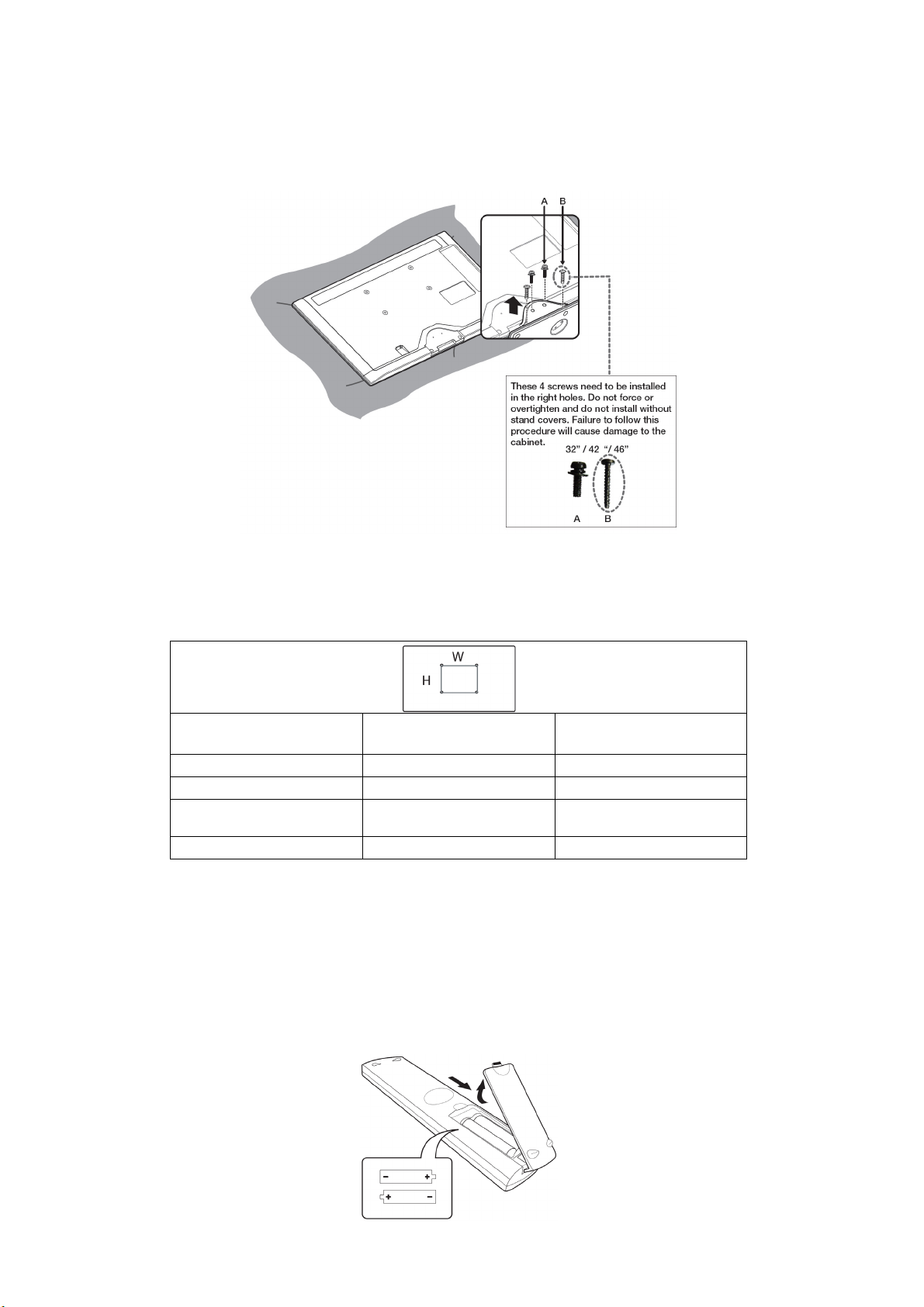
Detaching the Stand Neck for Wall Mounting
Caution
• Please use with care while disassembling the cabinet, stand, and pillar for wall mounting.
• Detach the stand neck in the correct direction.
• Do not remove the stand neck from the TV unless mounting it with an optional wall mount
Loosen the 4 screws that secure the stand neck by using a cross-head screwdriver. Remove the stand cover from the TV set.
Note
• To attach the stand neck, perform the steps in reverse order.
• Do not overtighten the screws and install the TV set without the stand cover.
Wall Mounting
TV screen size (Inches)
LC-46SV502L 400 x 400 mm Metric 6 x 14 mm
LC-46SV602B 400 x 400 mm Metric 6 x 16 mm
LC-42SV602B
LC-42SV502B
LC-32SV502B 200 x 100 mm Metric 4 x 14 mm
Note
• At the time of purchasing wall bracket, please check if there is enough space between the wall bracket and TV terminals for the terminal connection
VESA-compatible wall bracket
(millimeters) (W x H)
400 x 400 mm Metric 6 x 16 mm
Screw type
Preparation
Installing Batteries in the Remote Control Unit
1 Remove the battery compartment from the remote control.
2 Insert two "AAA" size batteries (supplied with the product).
LC-46SV502L
• Place the batteries with their terminals corresponding to the (+) and (-) indications in the battery compartment.
12
Page 13
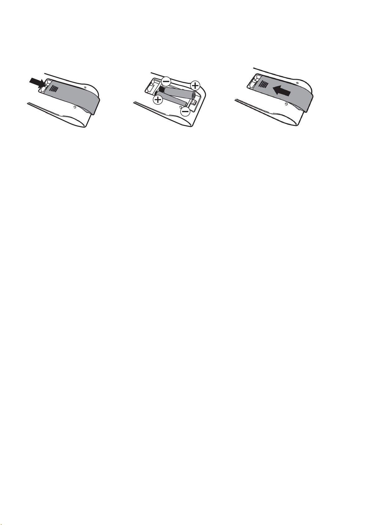
LC-32SV502B/LC-42SV502B/LC-42SV602B/LC-46SV602B
1 Remove the battery compartment from the remote control.
2 Insert two “AAA” size batteries (supplied with the product).
3 Close the battery cover.
LC-32SV502B/LC-42SV502B/LC-42SV602B/LC-46SV602B/LC-46SV502L
1
• Place the batteries with their terminals corresponding to the (+) and (-) indications in the battery compartment.
Cautuion
Improper use of batteries can result in chemical leakage or explosion. Be sure to follow the instructions below.
• Do not mix batteries of different types. Different types of batteries have different characteristics.
• Do not mix old and new batteries. Mixing old and new batteries can shorten the life of new batteries or cause chemical leakage of old batteries.
• Remove batteries as soon as they are worn out. Chemicals that leak from batteries come in contact with skin can cause a rash. If you find any chemical
leakage, wipe thoroughly with a cloth.
• The batteries supplied with this product may have a shorter life expectancy due to storage conditions.
• If you will not be using the remote control unit for an extended period of time, remove batteries from it.
• The batteries (batteries installed) shall not be exposed to excessive heat such as sunshine, fire or the like.
2 3
13
Page 14
LC-32SV502B/LC-42SV502B/LC-42SV602B/LC-46SV602B/LC-46SV502L
Using the Remote Control Unit
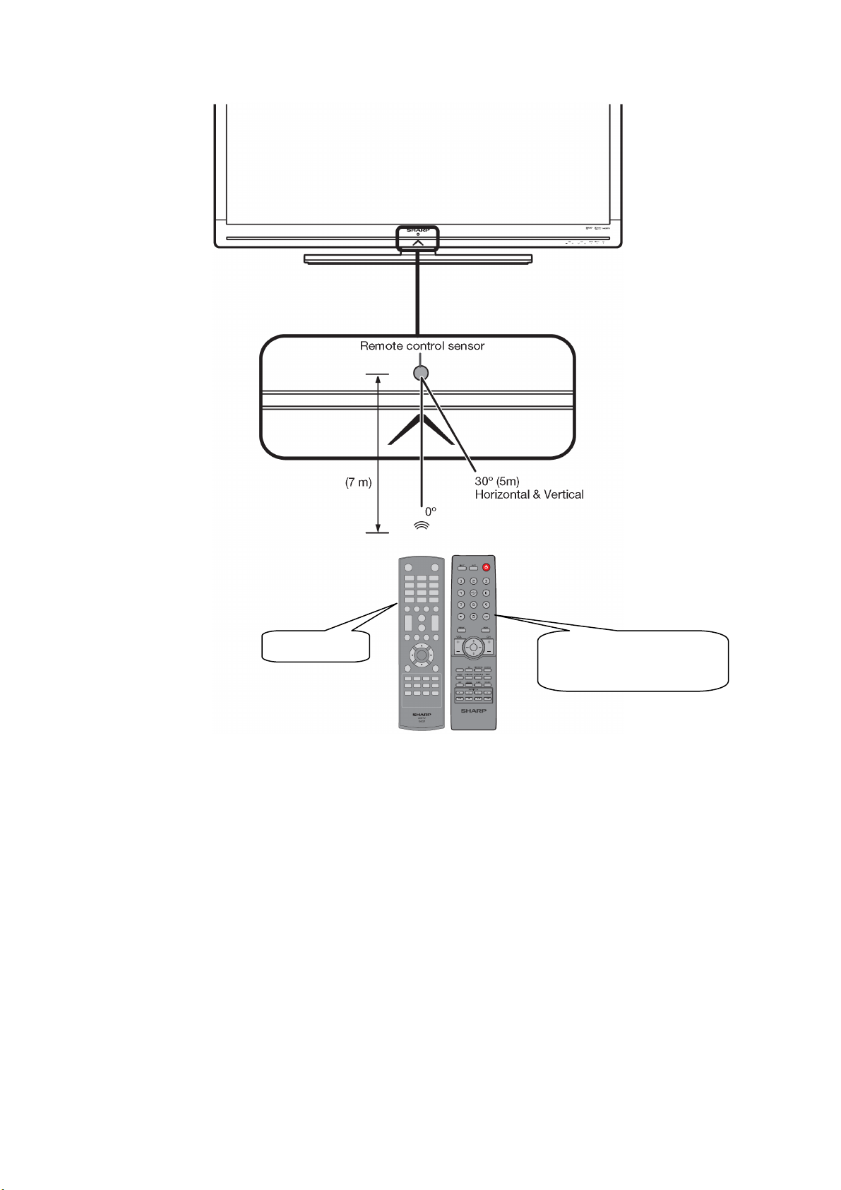
Use the remote control unit by pointing towards the remote control sensor on the TV. Objects between the remote control unit and the remote control
sensor may prevent proper operation.
LC-46SV502L
LC-32SV502B/LC-42SV502B/
LC-42SV602B/LC-46SV602B
14
Page 15
Appendix
Troubleshooting
LC-32SV502B/LC-42SV502B/LC-42SV602B/LC-46SV602B/LC-46SV502L
Information on the Software License for This Product
Software composition
The software included in this product is comprised of various software components whose individual copyrights are held by SHARP or by third parties.
Software developed by SHARP and open source software
The copyrights for the software components and various relevant documents included with this product that were developed or written by SHARP are
owned by SHARP and are protected by the Copyright Act, international treaties, and other relevant laws. This product also makes use of freely
distributed software and software components whose copyrights are held by third parties. These include software components covered by a GNU
General Public License (hereafter GPL), a GNU Lesser General Public License (hereafter LGPL) or other license agreement.
Acknowledgements
The following open source software components are included in this product:
Linux kernel/Modutils/Glibc/Zlib/Libpng
15
Page 16

LC-32SV502B/LC-42SV502B/LC-42SV602B/LC-46SV602B/LC-46SV502L
[3] DIMENSIONS
LC-46SV602B/LC-46SV502L
LC-42SV602B/LC-42SV502B
16
Page 17
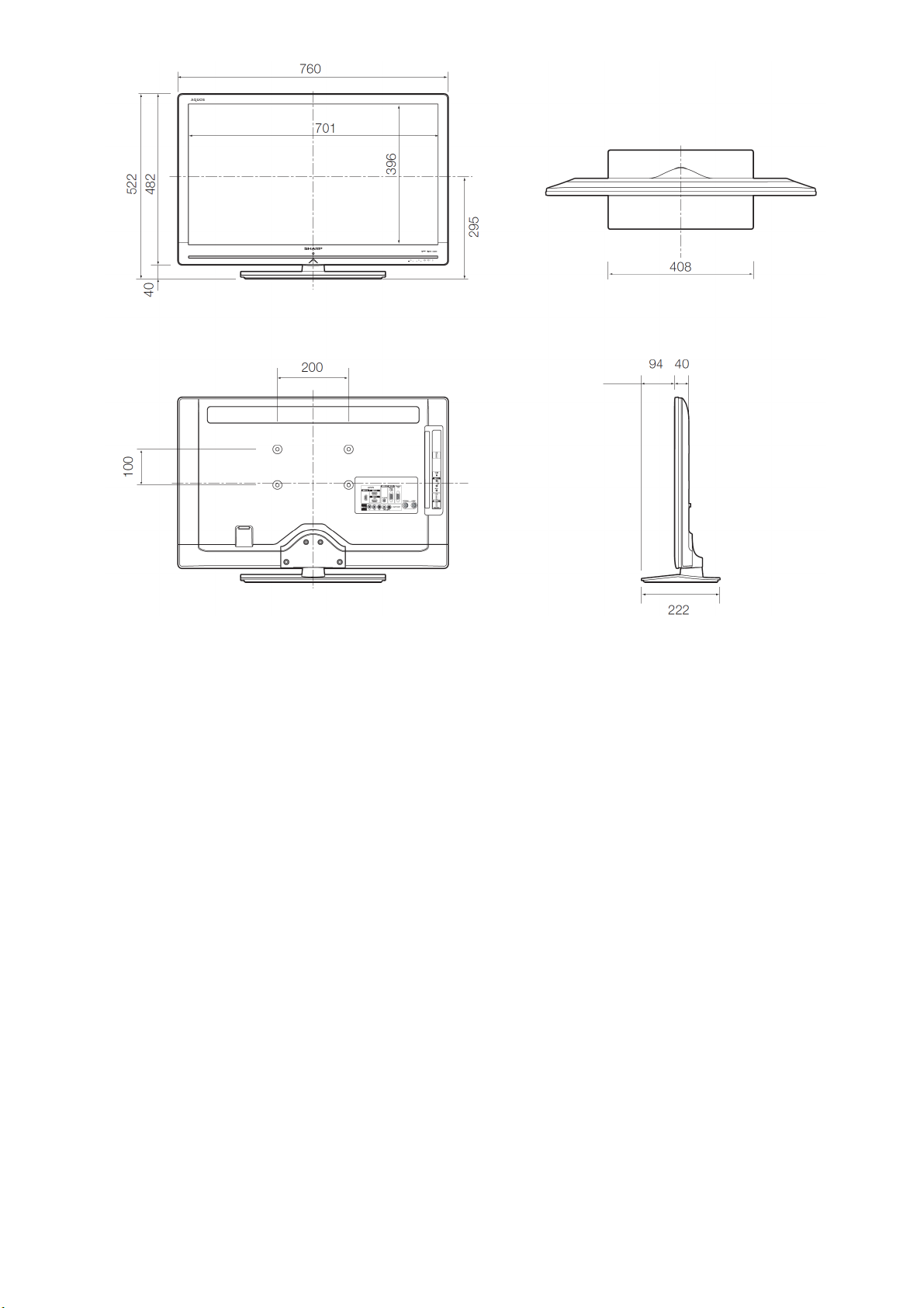
LC-32SV502B
LC-32SV502B/LC-42SV502B/LC-42SV602B/LC-46SV602B/LC-46SV502L
17
Page 18
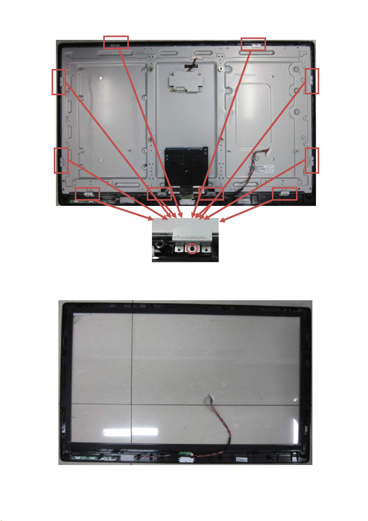
LC-32SV502B/LC-42SV502B/LC-42SV602B/LC-46SV602B/LC-46SV502L
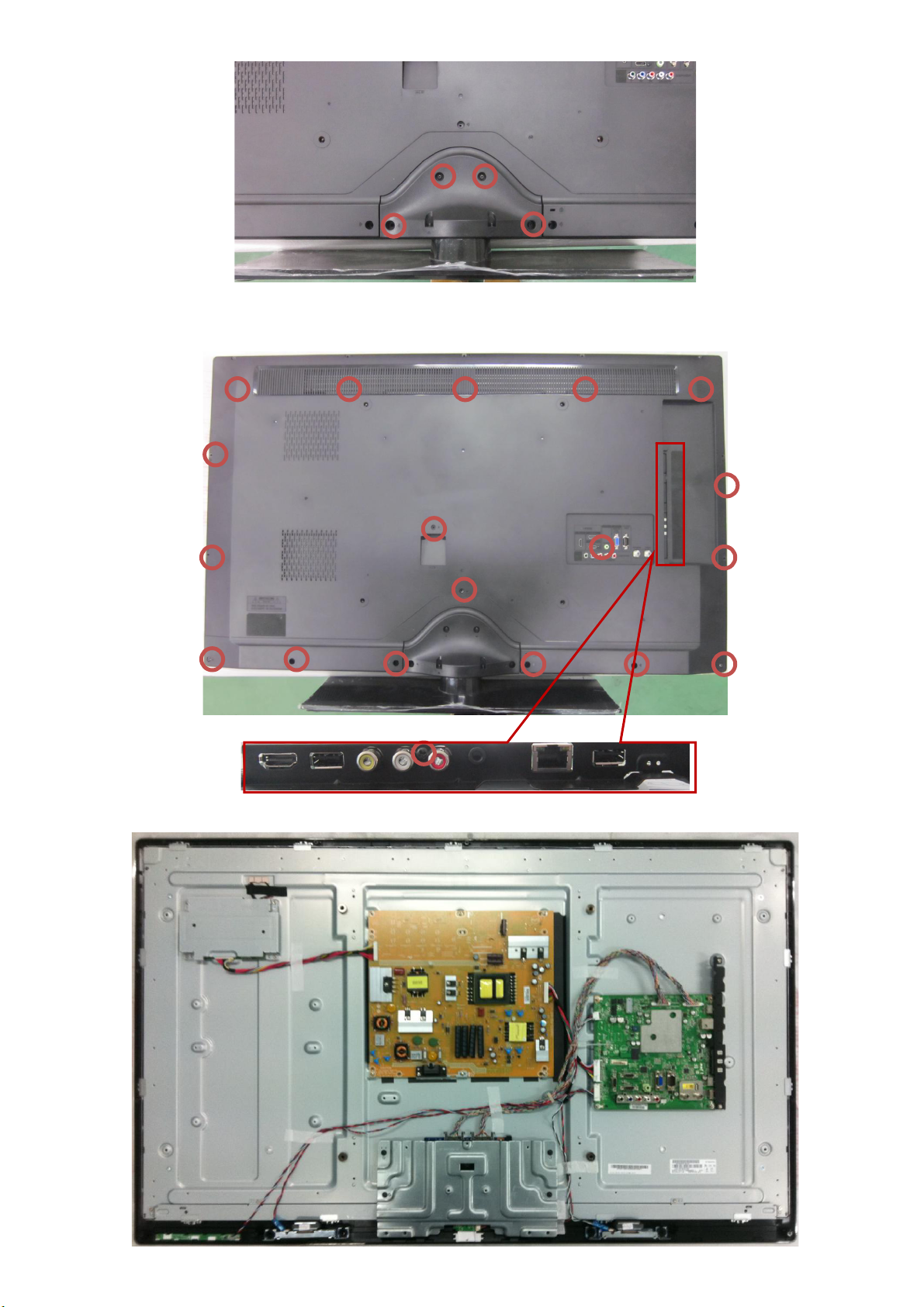
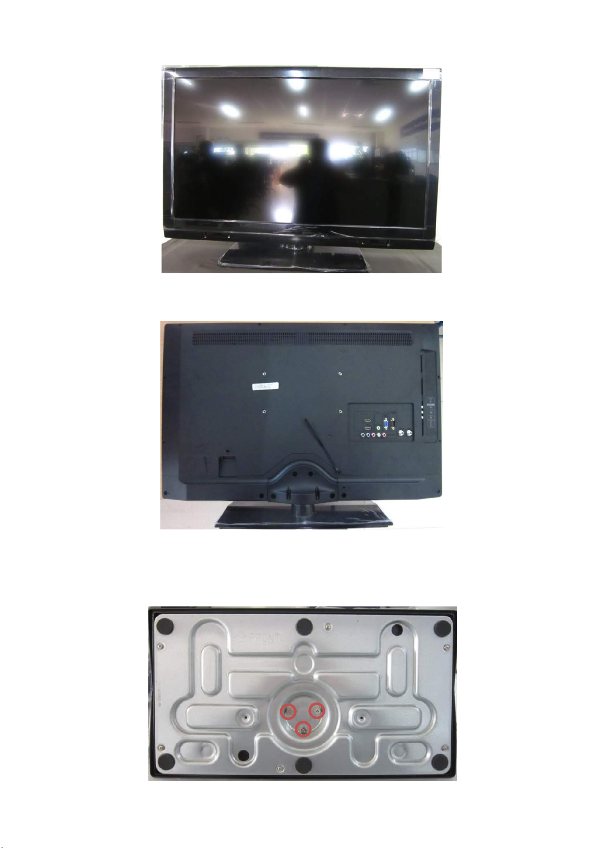
CHAPTER 2. REMOVING OF MAJOR PARTS
[1] ASSY/PANEL REMOVAL
Note: Put the TV face down on a safe surface that is covered by a soft and smooth cloth to avoid damaging LCD Panel.
Front View
Back View
Fig 1
Fig 2
Step 1. Remove the base.
A. Remove 4 screws as fig 3 and put out the base.
Fig 3
18
Page 19
LC-32SV502B/LC-42SV502B/LC-42SV602B/LC-46SV602B/LC-46SV502L
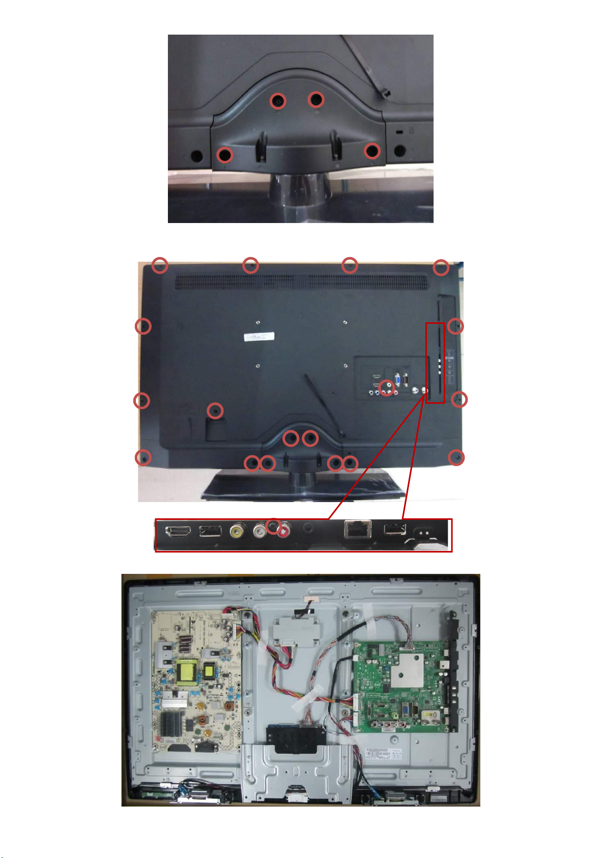
B. Remove 4 screws as Fig 4 to detach the bracket cover_stand.
Step 2. Remove the rear cover.
Remove 19 screws as Fig 5
Fig 4
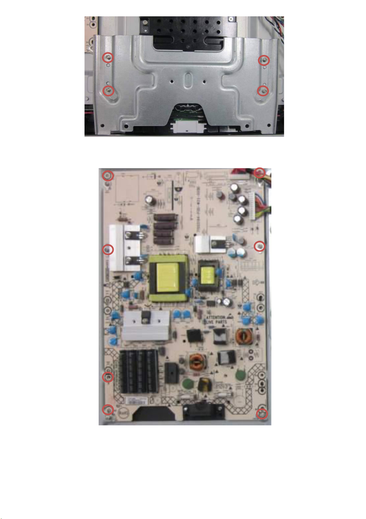
Step 3. Remove the bracket stand.
Remove 4 screws as Fig 6
Fig 5
19
Page 20
LC-32SV502B/LC-42SV502B/LC-42SV602B/LC-46SV602B/LC-46SV502L
Fig 6
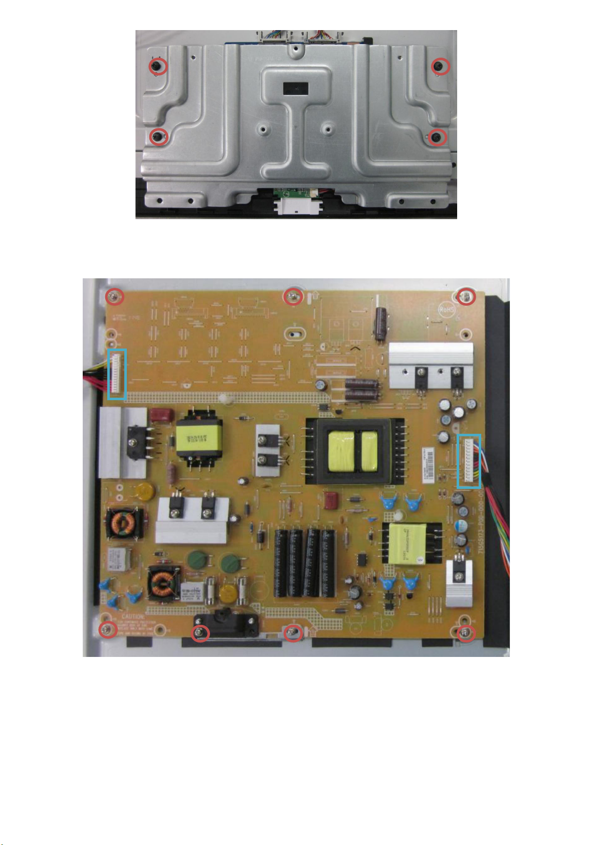
Step 4. Remove the power board.
Remove 7 screws and unplug 2 cables as Fig 7
Fig 7
20
Page 21
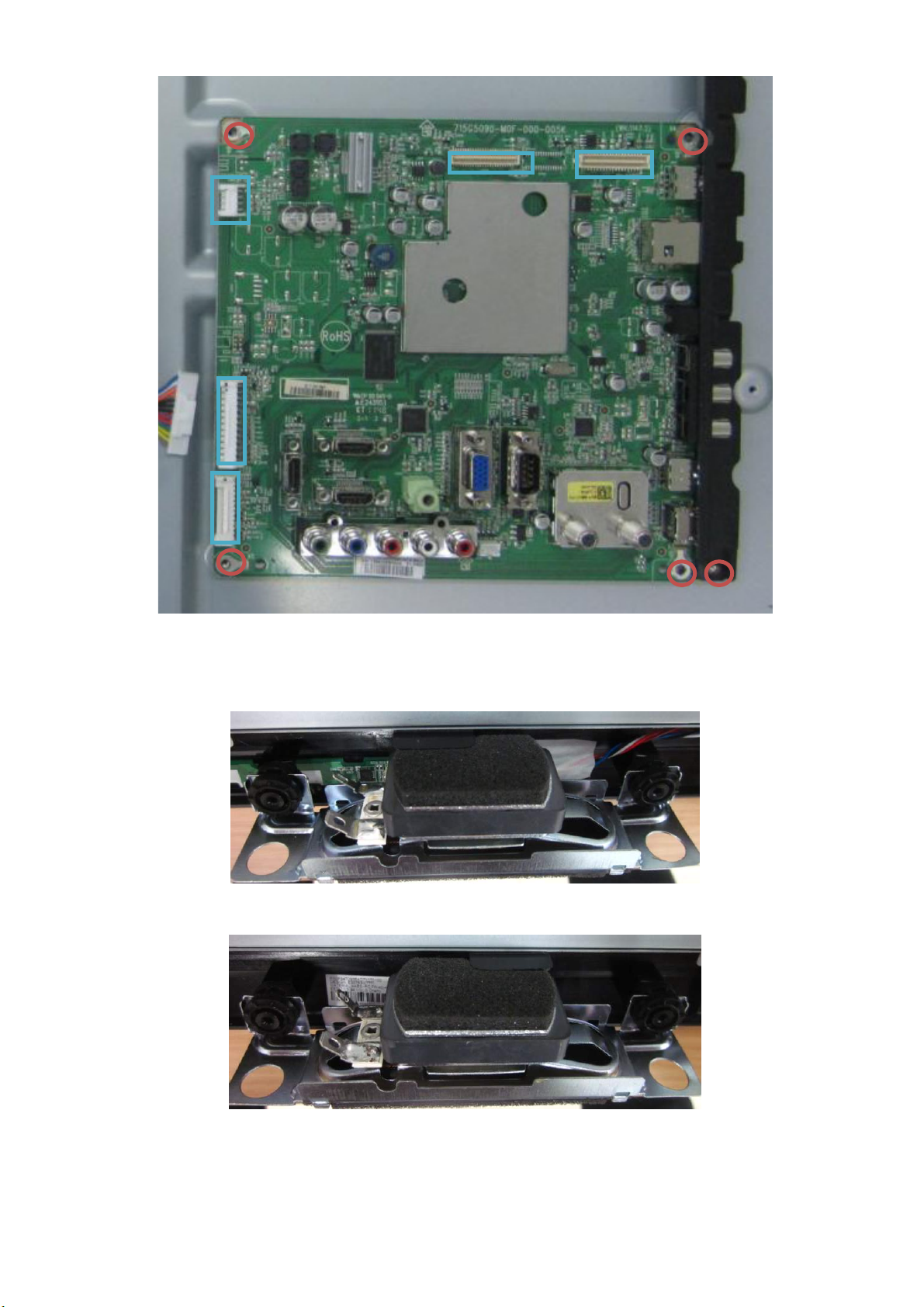
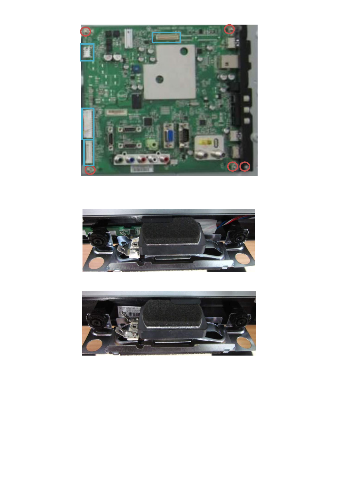
Step 5. Remove the scaler board.
Remove 5 screws and unplug 5 cables as Fig 8
LC-32SV502B/LC-42SV502B/LC-42SV602B/LC-46SV602B/LC-46SV502L
Step 6. Remove the speakers(L/R).
Remove as Fig 9 and Fig 10
Fig 8
Fig 9
Fig 10
21
Page 22
LC-32SV502B/LC-42SV502B/LC-42SV602B/LC-46SV602B/LC-46SV502L
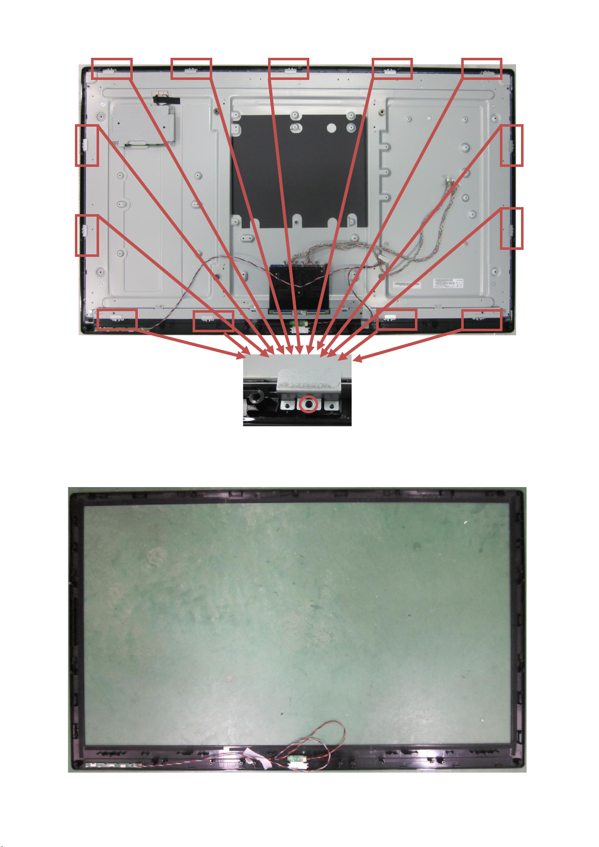
Step 7. Remove the bkt_panel and separate the panel and bezel.
Remove 13 screws as Fig 11
Step 8. Bezel assy.
The bezel assy as Fig 12
Fig 11
Fig 12
22
Page 23
Only for LC-32SV502B
Front View
Back View
LC-32SV502B/LC-42SV502B/LC-42SV602B/LC-46SV602B/LC-46SV502L
Fig 1
Step 1. Remove the base.
A. Remove 3 screws as fig 3 and put out the base.
Fig 2
Fig 3
23
Page 24
LC-32SV502B/LC-42SV502B/LC-42SV602B/LC-46SV602B/LC-46SV502L
B. Remove 4 screws as Fig 4 to detach the bracket cover_stand.
Step 2. Remove the rear cover.
Remove 19 screws as Fig 5
Fig 4
Fig 5
Step 3. Remove the bracket stand.
Remove 4 screws as Fig 6
24
Page 25
Step 4. Remove the power board.
Remove 7 screws and unplug 2 cables as Fig 7
LC-32SV502B/LC-42SV502B/LC-42SV602B/LC-46SV602B/LC-46SV502L
Fig 6
Fig 7
25
Page 26
LC-32SV502B/LC-42SV502B/LC-42SV602B/LC-46SV602B/LC-46SV502L
Step 5. Remove the scaler board.
Remove 5 screws and unplug 5 cables as Fig 8
Step 6. Remove the speakers(L/R).
Remove as Fig 9 and Fig 10
Fig 8
Fig 9
Fig 10
26
Page 27
LC-32SV502B/LC-42SV502B/LC-42SV602B/LC-46SV602B/LC-46SV502L
Step 7. Remove the bkt_panel and separate the panel and bezel.
Remove 10 screws as Fig 11
Step 8. Bezel assy.
The bezel assy as Fig 12
Fig 11
27
Page 28

LC-32SV502B/LC-42SV502B/LC-42SV602B/LC-46SV602B/LC-46SV502L
[2] SET RE-ASSEMBLY
To re-assemble the whole set, execute all processes in reverse order.
Note
a. While re-assembling, make sure that all cables are placed and connected in their original position.
b. Pay special attention not to damage the EMC foams at the SSB shielding. Check that EMC foams are put
correctly on their places.
28
Page 29
LC-32SV502B/LC-42SV502B/LC-42SV602B/LC-46SV602B/LC-46SV502L
CHAPTER 3. ADJUSTMENT PROCEDURE
[1] ADJUSTMENT PROCEDURE
1. OSD Menu
OSD tree - As following
Level 1 Level 2 Level 3 Level 4 Level 5 Attributes
Video
AV Mode User, Dynamic, Standard, Movie, Power Saver
Backlight 0~50~100
Brightness 0~50~100
Contrast 0~50~100
Tint => Hue -50~0~50
Sharpness 0~10~20
Gamma
Color Temperature
R Gain -100~100
G Gain -100~100
B Gain -100~100
C.M.S.-Hue R, Y, G, C, B, M, Reset
C.M.S.-Saturation R, Y, G, C, B, M, Reset
C.M.S.-Value R, Y, G, C, B, M, Reset
Flesh Tone On/Off
Blue Stretch On/Off
Gamma Adjustment Dark/Middle/Bright
Game Mode On/Off
HDMI Mode Auto/Graphic/Video
Effect Off/Low/Middle/High
Mode Mode 1/Mode 2
Demo Partition All/Right/Left
Demo
Adaptive Backlight On/Off
VGA Mode Graphic/Video
VGA => PC
Auto Adjust
H.Position 0~50~100
V.Position 0~50~100
Phase 0~31
Clock 0~255
3D
3D Mode Off/Auto/2D to 3D/Side by Side/Top and Bottom
L-R Switch On/Off
Depth of Field 0~32
3D to 2D Off/Right/Left
Audio
Sound Mode Personal/Rock/Pop/Live/Dance/Techno/Classic/Soft
Equalizer 1KHz -6~0~6
Equalizer 3KHz -6~0~6
Balance L50~0~R50
Bass 0~50~100
Treble 0~50~100
Color =>
Saturation
Color
Temperature
Advanced
Video
Equalizer
100Hz
Equalizer
300Hz
Equalizer
10KHz
0~50~100
Middle
Bright
Dark
User
Cool
Normal
Warm
Noise Reduction =>
Digital Noise
Reduction
MPEG Noise
Reduction
Adaptive Luma
Control => Active
Contrast
DI Film Mode =>
Film Mode
MJC => Motion
Enhancement
-6~0~6
-6~0~6
-6~0~6
Off/Low/Medium/Strong/Auto
Off/Low/Medium/Strong
Off/Low/Medium/Strong
Auto
Off
29
Page 30
LC-32SV502B/LC-42SV502B/LC-42SV602B/LC-46SV602B/LC-46SV502L
Equalizer Off/Rock/Pop/Live/Dance/Techno/Classic/Soft
Subwoofer Off/Low/Medium/High
Speaker
TV
Tuner Mode Cable/Air
Update CH
CH Skip Channel list
Audio Mode
A Channel list
B Channel list
C Channel list
D Channel list
All Data Clear
Application On/Off
Auto Startup On/Off
Application List
Network if RJ45 connector exist
Internet Connection On/Off
Connection Type
Scan Show current access point
Manual
Auto
PIN
PBC
Information
Address Type Auto/Manual
IP Address
Primary DNS
Secondary DNS
Connection Test
Applications
DLNA On/Off
Netflix
Deactivate
ESN
Vudu
Deactive
My Network Places On/Off
Setup
Language
View Mode Stretch
Sound
Surround
SPIDIF Type
=> Digital
Output Type
Auto Volume
Control
Wall Mount
Audio Setup
Auto CH
Search
Analog CH
Name Edit
Analog CH
Fine Tune
Digital CH
Tuning
Digital Dual
Mono
Favorite
Channels
GINGA
Settings
Configuration
=> Network
Setup
Software
Update
On/Off
1. if "CEC ARC Func" in factory meny is YES
=> Auto (CEC)/On/Off
2. if "CEC ARC Func" in factory meny is NO
=> On/Off
Off/PCM/Dolby Digital
On/Off
Yes/No
Wireless Setup =>
Wireless Setting
IP Setting => IP
Setup
Subnet Mask =>
Netmask
Default Gateway
=> Gateway
Major
Major & Minor
Stereo
SAP
Mono
Main + Sub
Main
Sub
30
Page 31

LC-32SV502B/LC-42SV502B/LC-42SV602B/LC-46SV602B/LC-46SV502L
Side bar
Smart stretch
Zoom
Dot by Dot
DPMS On/Off
Blue Mute On/Off
Time Setup
Time Zone
Time
Date
Time
Power On Timer On/Once/Off
Timer
Power Off Timer On/Once/Off
Timer
Sleep Timer Off/10/20/30/40/50/60/90/120 Minutes
Auto Sleep Off/1/2/5 Hours
Caption Setup
Caption Off/On/On-Mute
Superimpose Setup Off/Language1/Language2
Digital Caption Style
Caption Style As Broadcaster/Custom
Font Size Large/Small/Medium
Font Style Style1-3
Font Color Black/White/Green/Blue/Red/Cyan/Yellow/Magenta
Font Opacity Solid/Translucent/Transparent
Background Color Black/White/Green/Blue/Red/Cyan/Yellow/Magenta
Window Color Black/White/Green/Blue/Red/Cyan/Yellow/Magenta
Window Opacity Solid/Translucent/Transparent
Location Store/Home
DCR Demo Off/On
Input Label Input list
APP 1 Netflix/USB Media/Home Network
APP 2 Netflix/USB Media/Home Network
APP 3 Netflix/USB Media/Home Network
Reset
Demo Mode
Demo Mode Select Connected TV/Feature Demo/Auto Play
Auto Play Setting Continuous/10 min./20 min.
Power Control
Audio Only Off/On
No Signal Off Enable/Disable
Power Saving Off/On
No Operation Off Enable/Disable
Version Info
Reset
Parental
Password
Channel Block Channel list
Digital Rating
Program Block
Rating Enable On/Off
U.S. TV Ratings None/TV-Y/TV-Y7/TV-G/TV-PG/TV-14/TV-MA
U.S. Movie Ratings None/G/PG/PG-13/R/NC-17/X
DivX(R)
Registration
Program Title
Display
FAV APP Key
Assign
Icon Light Up
Setting
Auto
Synchronization
Power On
Channel
Analog Closed
Caption
Digital Closed
Caption
Yes/No
Off/On
No Operation To
Sleep
CC1/CC2/CC3/CC4/TEXT1/TEXT2/TEXT3/TEXT4
Language 1 - 8
Background
Opacity
Off/1/2/4 Hours
On/Off
Solid/Translucent/Transparent
Automatic
As Broadcaster/GMT+ 0:00/GMT+ 1:00/ GMT+
2:00/GMT+ 3:00/GMT+ 3:30/GMT+ 4:00/ GMT+
4:30/GMT+ 5:00/GMT+ 5:30/GMT+ 5:45/GMT+
6:00/GMT+ 6:30/GMT+ 7:00/GMT+ 8:00/GMT+
9:00/GMT+ 9:30/GMT+ 10:00/GMT+ 11:00/GMT+
12:00/GMT+ 12:45/GMT+ 13:00/GMT- 12:00/GMT11:00/GMT- 10:00/GMT- 9:00/GMT- 8:00/GMT7:00/GMT- 6:00/GMT- 5:00/GMT- 4:00/GMT- 3:30/GMT3:00/GMT- 2:00/GMT- 1:00
31
Page 32

LC-32SV502B/LC-42SV502B/LC-42SV602B/LC-46SV602B/LC-46SV502L
Age Rating Off/Below 10/Below 12/ Below 14/Below 16/Below 18
Content Rating
Input Block Input list
New Password
Confirm Password
Clean All
USB
Multi-Media
Option
CEC Setup
CEC Function On/Off
Auto Turn Off On/Off
Multi-Media
Change
Password
DivX(R)
Registration
DivX(R)
Deactivation
Canadian English
Ratings
Canadian French
Ratings
E/C/C8+/G/PG/14+/18+
E/G/8 ans+/13 ans+/16 ans+/18 ans+
Off/Drugs/Violence/Sex/Violence & Drugs/Sex &
Drugs/Violence & Sex/Violence, Sex & Drugs
32
Page 33

LC-32SV502B/LC-42SV502B/LC-42SV602B/LC-46SV602B/LC-46SV502L
2. ADC Adjustment and White Balance Adjustment
It’s no need to do the white balance for this model, do ADC only.
1. Turn on the TV, press “Menu”, then press number key 1 + 9 + 9 + 9 and “RETURN”, it will achieve the factory mode. Select the item of Current source
and press right key to choose computer
2. Select the item of WD Pat, choose 80(80IRE), fix the item of Scalar G Gain, adjust the item of Scalar R B Gain, choose Color temp. and press right key
to continue adjustment; Choose 20(20IRE), fix the item of Scalar G Offset, adjust the item of Scalar R B Offset, choose Color temp. and press right key to
continue adjustment.
Color Temp.
Normal Warm Cool
x (center) 0.2850 0.0090 0.3130 0.0090 0.2740 0.0090
y (center) 0.2930 0.0090 0.3210 0.0090 0.2740 0.0090
33
Page 34

LC-32SV502B/LC-42SV502B/LC-42SV602B/LC-46SV602B/LC-46SV502L
[2] SOFTWARE UPGRADE PROCEDURE
FW Upgrade
I. Copy the software firmware (*_loader.pkg) to USB drive.
II. Modify the pkg’s filename to “upgrade_loader.pkg”
III. Insert the USB drive to TV USB port.
IV. TV AC power off AC power on
V. TV will upgrade by itself after detect the USB drive condition and the content of the pkg file.
Note: TV’s LED will flash during upgrade process
VI. After finish upgrade process, TV will reboot by itself.
VII. Remove USB drive from TV.
VIII. Check if the software version is correct.
(Menu / Setup / Version info/ software version)
34
Page 35

The Writing VGA & HDMI EDID
Take other model for example
Step1. Ready for writing EDID
Tool: 715G089-B/C
Cable: a USB cable, a VGA cable, and a DVI to HDMI cable.
715G089-B/C USB cable
LC-32SV502B/LC-42SV502B/LC-42SV602B/LC-46SV602B/LC-46SV502L
VGA cable DVI to HDMI cable
USB port driver TpvEdid.exe (ISP TOOL) VGA&HDMI EDID
35
Page 36

LC-32SV502B/LC-42SV502B/LC-42SV602B/LC-46SV602B/LC-46SV502L
Step2. Connection for VGA EDID writing and turn on the TV
Connect to PC
USB port by USB
cable.
Step3. Install TPVedid tool.
Connect to TV
VGA port by
VGA cable.
3.1 Read the VGA EDID file.
1. Double click this icon to install.
2. Double click this icon to run.
2. Select VGA EDID file correctly.
36
1. Click “Read File”
Page 37

3.2 Select “FtdiUSB” communication type. And test the EDID.
2. Tick ”FtdiUSB(1)”
1. Click “FPD” to open
this interface.
LC-32SV502B/LC-42SV502B/LC-42SV602B/LC-46SV602B/LC-46SV502L
3. Click ”Text EDID”, if
communicate fluently, will
appears “edid write
protected”
3.3 Start to write EDID.
1. Click ”Write EDID” to start
writing. Blue “OK” represents
write EDID successfully.
37
Page 38

LC-32SV502B/LC-42SV502B/LC-42SV602B/LC-46SV602B/LC-46SV502L
3.4 Click “Read EDID”.
1.Click ”Read EDID” to start
reading EDID from TV. Blue
“OK” represents read EDID
successfully.
Step4. Click “FPD” to open another interface as follows to check the whether the info is the same as you loaded previously.
38
Page 39

LC-32SV502B/LC-42SV502B/LC-42SV602B/LC-46SV602B/LC-46SV502L
Step5. When the tool displays “NG” in the yellow blank, which represent writing failly. Please check the whether the connection of tool and cables is
nomal and retry. Another way is to change a new ISP board and retry.
39
Page 40

LC-32SV502B/LC-42SV502B/LC-42SV602B/LC-46SV602B/LC-46SV502L
p
CHAPTER 4. TROUBLESHOOTING TABLE
[1] TROUBLESHOOTING TABLE
Power unit operation check.
↓
Are the power cord and harness in the unit properly connected?
LINE_FILTER_UNIT: ↓ YES
Is F9901/F9902 normal?
POWER_UNIT
Is B+_main output? (Set the main power SW to ON.)
↓YES
↓YES
Is a voltage of +5.2V applied to pin (2,3) of connector (CN9304)?
(Set the main power SW to ON.)
↓YES
Are 12 and 24V output as for the power on/off switch when it is on?
The sound is not emitted from the speaker though the picture has come out.
↓
No sound output in all modes?
TERMINAL UNIT: ↓
Is the audio signal output of IC U401 normal?
↓YES
Is audio signal input to pin (27/28/29/30) of IC U608 (AMP)?
↓YES
Is MUTE circuit [AMP_MUTE_LINE, POWERUP_LINE] normal?
↓YES
Is the audio signal output of pin (1,2) (R) and pin (3,4) (L) of
CN605(AOUDIO-CONNECTOR) normal?
↓YES
Check Speaker (right and left) and wire harness.
NO
NO
NO
NO
NO
NO
NO
NO
NO
Connect the power cord and harness properly, and turn on the
LINE_FILTER_UNIT:
Isn't NR9901,NR9902,L9901,L9902(for 32”),L9903,etc. out of
order? Moreover, whether the short-circuit with the
circumference circuit is checked.
POWER_UNIT:
BD9901, FB902, FB9805, FB806, FB9301(for 32”),D9301, etc.
out of order?
Moreover, whether the short-circuit with the circumference circuit
Does the PFC circuit operate normally?
The circuit around the protection circuit etc. is checked.)
Does the switching circuit operate normally?
Check circuit around the primary side (IC9301, T9301, D9302(for
32”),D9307,etc.), the secondary side (D9308, L9304, ZD9303,
etc.), and the protection circuit.
Does the inverter circuit operate normally?
Check circuit around the primary side (IC9101, IC9103(for
32”),T9101, Q9101, etc.), the secondary side (IC9106, D9102,
D9103, etc.), and the protection circuit.
Check IC U401 and its peripheral circuits.
Check the line between IC U401 and IC U608.
Check the AMP_MUTE_LINE and POWERUP_LINE.
(Q609,etc.)
Check IC U602 and its peripheral circuits.
ower.
40
Page 41

LC-32SV502B/LC-42SV502B/LC-42SV602B/LC-46SV602B/LC-46SV502L
(
No sound (during the reception of TV broadcasting)
↓
Does not the sound go out though the picture has come out when TV is received?
MAIN UNIT: ↓
Is the IF signal output from pin (1/2/4/5) of Tuner (TU101)?
NO
↓YES
Is the IF signal sent to pin (AM24/AL24) of IC U401?
NO
↓YES
Refer to “No sound output in all modes”.
No sound from external input devices (1)
↓
Does not the sound of the audio signal input to Component go out?
MAIN UNIT: ↓
Is the audio signal properly sent to pin (8)(YPbPr_L_In) and pin
(11)(YPbPr_R_In) of CN108?
NO
↓YES
Is the audio signal properly sent to pin (AL29) (YPbPr_L_In1) and
pin (AL31) (YPbPr_R_In1) of IC U401?
NO
↓YES
Refer to “No sound output in all modes”.
No sound from external input devices (2)
↓
Does not the sound of the audio signal input to (Composite, Y/C) go out?
MAIN UNIT: ↓
Is the audio signal properly sent to pin (4) (AV1_AudioLIN) and pin
(7) (AV1_AudioRIN) of CN101?
NO
↓YES
Is the audio signal properly sent to pin (AM30) (AV_L_In0) and pin
AM32) (AV_R_In0) of IC U401?
NO
↓YES
Refer to “No sound output in all modes”.
Check the tuner and its peripheral circuits. Replace as required.
Check IC U401 its peripheral circuits.
Check the connection to CN108 and the external input device.
Check the line between CN108 and IC U401.
Check the connection to CN101and the external input device.
Check the line between CN101 and IC U401.
41
Page 42

LC-32SV502B/LC-42SV502B/LC-42SV602B/LC-46SV602B/LC-46SV502L
No sound from external input devices (3)
↓
Does not the sound of the audio signal input to (VGA) go out?
MAIN UNIT: ↓
Is the audio signal properly sent to pin (2) (VGA_Audio_L_In) and
pin (3) (VGA_Audio_R_In) of CN104?
NO
Check the connection to CN104 and the external input device.
↓YES
Is the audio signal properly sent to pin (AL30) (VGA_L_In) and pin
(AL32) (VGA_R_In of IC U401?
NO
Check the line between CN104 and IC U401.
↓YES
Refer to “No sound output in all modes”.
No sound from external input devices (4)
↓
Does not the sound of the audio signal input to (HDMI1/2) go out?
↓
Is picture of the signal input from HDMI 1/2 displayed?
NO
Refer to “Does not the picture of the HDMI signal input to
HDMI1/2 go out?”.
↓YES
Refer to “No sound output in all modes”.
No picture on the display (1)
↓
The picture doesn't appear in all modes.
MAIN UNIT: ↓
Is LVDS signal output from 1st_channel and 2nd_channel of IC U401 in each mode?
(O0/O1/O2/O3/OCK)
↓NO
YES ↓
Is the above-mentioned LVDS signals output to connector CN403?
NO
Check IC U401 and its peripheral control circuits.
Check the line between IC U401 and CN403.
↓YES
Is LCD controller's control signal normal?
PANEL_UNIT: ↓YES
Similarly, is the LVDS signal input to connector of the panel
module?
NO
NO
Control signals BRIGHT_ADJ, INVERTER_ON_OFF,
PANEL_VCC_ON/OFF, and it peels off and whether normality is
checked.
Wire harness is checked. (Main board to Panel module )
↓YES
Check the panel module.
42
Page 43

LC-32SV502B/LC-42SV502B/LC-42SV602B/LC-46SV602B/LC-46SV502L
No picture on the display (2)
↓
Does not the picture come out when VHF/UHF is received?
TERMINAL UNIT: ↓
Is TUNER_CVBS signal output from TUNER (TU101)?
NO
MAIN_UNIT: ↓YES
Is picture signal input from pin TUNER (TU101) to IC U401?
NO
↓YES
Refer to “The picture doesn't appear in all modes.”
No picture on the display (3)
↓
Does not the picture come out when TV is received?
TERMINAL UNIT: ↓
Is the voltage of regulation for a TUNER circuit and the power
supply terminal of IC U401 supplied?
↓YES
Is IF signal output from pin (1/2/4/5) of TUNER (TU101) to pin
(AM24/AL24) of IC U401?
MAIN_UNIT: ↓YES
Do X401 (27MHz) oscillate?
↓YES
Refer to “The picture doesn't appear in all modes.”
NO
NO
NO
<External input (Component)>No picture on the display (4)
↓
Does not the picture of the component video signal input to Component go out?
TERMINAL_UNIT: ↓
Is Component Y/Pb/Pr signal sent to pin (2)/Y, (4)/Pb, (6)/Pr of
AV1(CN108) ?
MAIN_UNIT:
Is Component Y/Pb/Pr signal sent to pin (AM18)/Y, (AM19)/Pb,
(AK19)/Pr of IC U401?
↓YES
NO
NO
↓YES
Refer to “The picture doesn't appear in all modes.”
Check whether I2C is normally accessed between TU101 and IC
U401.
Check the line between IC U401 and TU101.
Each power supply circuit is checked.
Check the tuner, IC U401 and their peripheral circuits. Replace
as required.
Check X401 and its peripheral circuits.
Check the setting of an external input device that connects of
CN108.
Check the line between IC U401 and CN108.
43
Page 44

LC-32SV502B/LC-42SV502B/LC-42SV602B/LC-46SV602B/LC-46SV502L
<External input AV (Composite)>No picture on the display (5)
↓
Does not the picture of the composite video signal input to AV(Composite) go out?
TERMINAL UNIT: ↓
Is CVBS signal sent to pin (2) of AV (CN101) ?
MAIN_UNIT: ↓YES
Is CVBS signal sent to pin (A19) of IC U401?
Refer to “The picture doesn't appear in all modes.”
↓YES
NO
NO
Check the setting of an external input device that connects of
CN101.
Check the line between IC U401 and CN101.
<External input HDMI1 >No picture on the display (6)
↓
Does not the picture of the HDMI signal input to HDMI1 go out?
MINI AV_UNIT: ↓
Is the HOT_PLUG detection function of pin (19) of a HDMI terminal
(CN503) normal?
NO
Check the line between pin (35) of IC U505 and CN503.
Check the connection and setup with the external HDMI devices.
YES
Is TMDS signal input into pin ((3,4)/( RR0X0), (5,6)/( RR0X1),
RR0X2), (1,2)/( RR0XC)) of IC U502?
(7,8)/(
Is TMDS signal output from pin ((56/57/58/59/60/61/62/63)/(RX1) of
IC U502?
Refer to “The picture doesn't appear in all modes.”
↓YES
↓YES
NO
NO
Check the line between IC U502 and CN503.
Check IC U502 and peripheral circuits.
<External input HDM2 >No picture on the display (7)
↓
Does not the picture of the HDMI signal input to HDMI2 go out?
MINI AV_UNIT: ↓
Is the HOT_PLUG detection function of pin (19) of a HDMI terminal
(CN5023) normal?
NO
Check the line between pin (41) of IC U502 and CN502.
Check the connection and setup with the external HDMI devices.
YES
Is TMDS signal input into pin ((13,14)/( RR1X0), (15,16)/( RR1X1),
RR1X2), (11,12)/( RR1XC)) of IC U502?
(17,18)/(
Is TMDS signal output from pin ((56/57/58/59/60/61/62/63)/(RX1) of
IC U502?
Refer to “The picture doesn't appear in all modes.”
↓YES
↓YES
NO
NO
Check the line between IC U502 and CN502.
Check IC U502 and peripheral circuits.
↓NO
↓NO
44
Page 45

LC-32SV502B/LC-42SV502B/LC-42SV602B/LC-46SV602B/LC-46SV502L
<External input HDMI1 >No picture on the display (8)
↓
Does not the picture of the HDMI signal input to HDMI3 go out?
MINI AV_UNIT: ↓
Is the HOT_PLUG detection function of pin (19) of a HDMI terminal
(CN504) normal?
NO
Check the line between pin (41) of IC U502 and CN504.
Check the connection and setup with the external HDMI devices.
YES
Is TMDS signal input into pin ((13,14)/( RR2X0), (15,16)/( RR2X1),
RR2X2), (11,12)/( RR2XC)) of IC U501?
(17,18)/(
Is TMDS signal output from pin ((56/57/58/59/60/61/62/63)/(RX1) of
IC U502?
Refer to “The picture doesn't appear in all modes.”
↓YES
↓YES
NO
NO
Check the line between IC U501 and CN504.
Check IC U502 and peripheral circuits.
<External input HDMI1 >No picture on the display (9)
↓
Does not the picture of the HDMI signal input to HDMI4 go out?
MINI AV_UNIT: ↓
Is the HOT_PLUG detection function of pin (19) of a HDMI terminal
(CN501) normal?
NO
Check the line between pin (45) of IC U502 and CN501.
Check the connection and setup with the external HDMI devices.
YES
Is TMDS signal input into pin ((21,22)/( RR3X0), (23,24)/( RR3X1),
RR1X2), (19,20)/( RR1XC)) of IC U502?
(25,26)/(
Is TMDS signal output from pin ((56/57/58/59/60/61/62/63)/(RX1) of
IC U502?
Refer to “The picture doesn't appear in all modes.”
↓YES
↓YES
<External input VGA>No picture on the display (10)
NO
NO
Check the line between IC U502 and CN501.
Check IC U502 and peripheral circuits.
↓
Does not the picture of the PC IN(ANALOG) video signal input to VGA (15pin-D-SUB terminal) go out?
TERMINAL_UNIT: ↓
Is R/G/B/H/V signal sent to pin (1)/R, (2)/G, (3)/B, (13)/H, (14)/V of
VGA (CN103)?
MAIN_UNIT: ↓YES
Is R/G/B/H/V signal sent to pin (AM15)/R, (AK15)/G, (AK13)/B,
(AL13)/H, (AM13)/V of IC U401?
Refer to “The picture doesn't appear in all modes.”
↓YES
NO
NO
Check the setting of an external input device that connects of
CN103.
Check the line between IC U401 and CN103.
↓NO
↓NO
45
Page 46

LC-32SV502B/LC-42SV502B/LC-42SV602B/LC-46SV602B/LC-46SV502L
CHAPTER 5. MAJOR IC INFORMATIONS
[1] MAJOR IC INFORMATION
2.1 U401(MT5395LPOJ/B)
General Description
The MediaTek MT5395LPOJ family is a backend decoder and a TV controller and offers high integration for advanced applications. It combines a
transport de-multiplexer, a high definition video decoder, an AC3 audio decoder, a four-link LVDS transmitter, a mini-LVDS transmitter, a V-by-One
transmitter, and an NTSC/PAL/SECAM TV decoder with a 3D comb filter (NTSC/PAL). The MT5395LPOJ enables consumer electronics manufactures to
build high quality, low cost and feature-rich DTV.
World-Leading Audio/Video Technology: The MT5395LPOJ supports Full-HD MPEG1/2/4/DiviX/VC1/RM/H.264/AVS video decoder standards, and
JPEG. The MT5395LPOJ also supports MediaTek MDDiTM de-interlace solution can reach very smooth picture quality for motions. A 3D comb filter
added to the TV decoder recovers great details for still pictures. The special color processing technology provides natural, deep colors and true studio
quality video. Also, the MT5395LPOJ family has built-in high resolution and high-quality audio codec.
Rich Features for High Value Products: The MT5395LPOJ family enables true single-chip experience. It integrates high-quality HDMI1.4, high speed
VGA ADC, four-link LVDS, mini-LVDS, V-by-One, USB2.0 receiver, Ethernet MAC+PHY, TCON and panel overdrive.
All New Full-HD 120Hz Experience: The MT5395LPOJ family enables customers a true Full- HD 120Hz experience. It integrates high-quality Full-HD
ME/MC technology.
Key Features:
1. Worldwide multi-standard analog TV demodulator
2. A transport demultiplexer
3. A muti-standard video decoder
4. A H.264 HD720p video encoder
5. An AC3/MPEG2 audio decoder
6. HDMI1.4 receiver
7. Audio codec
8. TCON
9. Ethernet MAC+PHY
10. True 120Hz Full HD MJC
11. Panel overdrive control
12. Local dimming
13. Four-link LVDS, mini-LVDS, V-by-one transmitters
Note: All packages are lead free
Host CPU
ARM1176JZFS-700MHz
Supports Vector Floating-Point (VFP) coprocessor
16K I-Cache and 16K D-Cache
128K L2 Cache
14K Boot ROM
JTAG ICE interface
Watch Dog timers
Transport Demultiplexer
New generation 2 demux design
Supports two serial transport stream input with one serial transport stream input
Supports ATSC, DVB-T, DVB-C transport stream input
Supports DES / 3-DES / DVB / AES / Multi-2 de-scramblers
Up to 8 even/odd keys for descrambling
Supports 32 PID filters and 32 section filters
Supports 32 PID filters for recording
Supports hardware CRC-32 check
Supports PCR recovery function
Supports a micro-processor for stream processing and video start code detection
46
Page 47

LC-32SV502B/LC-42SV502B/LC-42SV602B/LC-46SV602B/LC-46SV502L
MPEG2 Decoder
MPEG MP@ML, MP@HL
Supports de-blocking filter
MPEG1 Decoder
MPEG4 Decoder
ASP@L5
H.264 (MPEG4.10 / AVC) HD Decoder
MP@L4.0, HP@L4.0, constrained BP@L3 video standard
VC-1 (SMPTE421M) Decoder
MP@HL, AP@L3(Partial Support, support up to 1920x1080)
WMV9 decoder MP@HL
DivX (XviD) Decoder
DIVX3 / DIVX4 / DIVX5 / DIVX6 / DIVX HD / DIVX PLUS
AVS Decoder
Jizhun profile @Level 6.0.1
RMVB Decoder
RealVideo8/9/10
Soreson H.263
MVC
H.264 stereo high profile 48fps
H.264 HD720p Encoder
MP@L3.1(main), BP@L3.1(baseline) video standard
1280x720p encoder
Supports CBR, B-frame and CABAC
Search range is up to +/- 160 (horizontal), +/-80(vertical)
Still Image decoding
JPEG (base-line or progressive)
De-mosquito engine
For all AV inputs
ME/MC Engine
Adopt 2nd generation 3-frame Halo reduced MEMC technology
Supports FHD 120Hz output
Supports motion judder cancellation for 24p/25p/30p input sources
Supports 24Hz/30Hz/60Hz to 120Hz, 25Hz/50Hz to 100Hz in 100/120Hz panel
Supports 24Hz/30Hz to 60Hz, 25Hz to 50Hz in 50/60Hz panel
Supports left/right video processing comparison function without additional DRAM resources for customers’ demonstration
2D Graphics
Supports multiple color modes
Point, horizontal/vertical line primitive drawings
Rectangle fill and gradient fill functions
Bitblt with transparent options
Alpha blending and optional pre-multiplied alpha composition Bitblt
Stretch Bitblt
YCbCr to RGB color space conversion
Supports index to direct mode bitblt
Image Resizer
Supports 16bpp/32bpp direct color format
Supports 420/422 video format
Supports 420/422/444 JPEG format
Arbitrary ratio vertical/horizontal scaling of video, from 1/128X to 128X
Simple DMA
47
Page 48

LC-32SV502B/LC-42SV502B/LC-42SV602B/LC-46SV602B/LC-46SV502L
OSD Plane
Three linking list OSDs with multiple color mode and two of them has up-scaler
Video Plane
Supports video freeze and over scan
Flesh tone management
Gamma correction
Color Transient Improvement (CTI)
2D Peaking
Saturation/hue adjustment
Brightness and contrast adjustment
Black and White level extender
Adaptive Luma management
Automatic detect video, film and mixed-mode source
3:2/2:2 pull down source detection
Supports FHD motion-adaptive de-interlace
Supports excellent low angle image processing
Brilliant boundary shaping for moving object
Advanced non-linear panorama scaling
Programmable zoom viewer
Progressive scan output
Supports alpha blending for OSD on video plane
Dithering processing for flat panel display
Frame rate conversion
Supports FHD panel and VGA dot-to-dot
Supports PIP/POP, (dual de-interlace, one HD and one SD)
OD
Supports 120Hz/60Hz Full-HD and WXGA panel over drive
TCON
Flexible timing control with programmable timing
Horizontal timing control
Vertical timing control
Multi-line timing control
Multi-frame timing control
Supports gate power modulation timing
Supports 1/2/4/8 frame inversion, 1-line inversion, 2-line inversion, and could up to 255-line dot inversion
Local Dimming
Block division: up to 800 total blocks, up to 100 horizontal blocks
Supports 50K ~ 50M SPI clock rate
LVDS
Supports 6/8/10-bit one-link, 6/8/10-bit dual-link, or 6/8/10-bit four-link LVDS transmitter
Built-in spread spectrum for EMI performance
Programmable panel timing output
Mini-LVDS
Dual port 10-bit 8 pairs mini-LVDS output for FHD 120Hz, FHD 60Hz, WXGA 60Hz panels
Dual port 8-bit 6 pairs mini-LVDS output for FHD 120Hz, FHD 60Hz, WXGA 60Hz panels
Dual port 10-bit 4 pairs mini-LVDS output for FHD 60Hz panel
Dual port 8-bit 3 pairs mini-LVDS output for FHD 60Hz panel
Single port 10-bit 8 pairs mini-LVDS output for FHD 60Hz panel
Single port 8-bit 6 pairs mini-LVDS output for FHD 60Hz panel
Single port 6/8-bit 6 pairs mini-LVDS output for WXGA 60Hz panel
Single port 6/8-bit 3 pairs mini-LVDS output for WXGA 60Hz panel
48
Page 49

LC-32SV502B/LC-42SV502B/LC-42SV602B/LC-46SV602B/LC-46SV502L
Dual port 6/8-bit 3 pairs mini-LVDS output for WXGA 60Hz panel
V-by-One
Supports 8/10/12-bit 4 lane FHD 120Hz panels
Supports 8/10/12-bit 2 lane FHD 60Hz panels
Supports 8/10/12-bit 1 lane WXGA 60Hz panels
Supports spread spectrum for EMI performance
CVBS In
On-chip 54 MHz 10-bit video ADC
Supports PAL (B,G,D,H,M,N,I,Nc), NTSC, NTSC-4.43, SECAM
NTSC/PAL supports 3D/2D comb filter
Built-in motion-adaptive 3D Noise Reduction
VBI data slicer for CC/TT decoding
Supports 2 S-Video
Max. Supports 3-channel CVBS
Supports SCART connector
VGA In
Supports VGA input up to UXGA 162 MHz
Supports full VESA standards
Component Video In
Supports two component video inputs
Supports 480i / 480p / 576i / 576p / 720p / 1080i / 1080p
Audio ADC
Supports 7-pair L/R input
Audio digital input
Supports 1 bit (2 channel) I2S audio input
HDMI Receiver
One channel HDMI1.4
Maximum data rate can be up to 3.3 GHz
Audio return channel
EIA/CEA-861B
CEC
Video bypass
TV bypass
CVBS Monitor (any AV input)
TV audio demodulator
Supports BTSC / EIA-J / A2 / NICAM / PAL FM / SECAM world-wide formats
Standard automatic detection
Stereo demodulation, SAP demodulation
Mode selection (Main/SAP/Stereo)
Audio DAC
Supports 4-pair audio DACs
DRAM Controller
48/32-bit DDR2/DDR3 interface
Supports DDR2 1053Mhz, DDR3 1323Mhz
Supports 512Mb or 1Gb DDR2 DRAM device and 1Gb or 2Gb DDR3 device, 48-bit data bus offers up to 768MB space
Supports DDR2-1066/DDR3-1333/DDR3-1600 device
Audio DSP
Supports Dolby Digital AC-3 decoding (ATSC)
MPEG-1 layer I/II decoding
Supports WMA / HE-AAC
49
Page 50

LC-32SV502B/LC-42SV502B/LC-42SV602B/LC-46SV602B/LC-46SV502L
Dolby Prologic II
Audio output: 5.1ch + 2ch (down mix) + 2ch(bypass)
Pink noise and white noise generator
Equalizer
Bass management
3D surround processing with virtual surround
Audio and video lip synchronization
Supports bass/treble
Automatic volume control
Supports 5-bit (10-channel) main audio I2S output interface, each of these channels is up to 24-bit resolution
S/PDIF interface
Supports SPDIF in bypass
One SPDIF out
Analog TV IF Demodulator
Supports world-wide analog TV standard
Accept Low IF frequency
Full digital AGC control and carrier recovery
Embedded SAW filter and IF Amplifier. Cost effective TV front-end structure and no more cost on:
External analog SAW filters (Video/Audio)
External analog IF demodulator
External peripheral circuit on CVBS signal data path
External SAW filter and IF VGA on tuner
Peripherals
Three built-in UARTs with Tx and Rx FIFO
Built-in Ethernet MAC and Ethernet PHY
Eight basic serial interfaces: one is for the tuner, two are the masters for general purpose, one is the slave for VGA DDC, the other four extra slave
serial interfaces used for HDMI EDID data (three are muxed with GPIO)
Four PWMs, one of them can be active in standby mode
IR receiver
Real-time clock and watchdog controller
Built-in 2-link USB2.0/1.1, one of them supports external hub
Built-in uP for standby mode
Supports SDIO interface
Supports smart card interface
Supports two serial flash or one serial and one NAND flash
Supports seven-input low-speed ADC
Supports boundary scan (JTAG)
IC Outline
The MT5395LPOJ is 27x27mm PBGA Package with 655 balls
3.3V/1.1V/1.2V and 1.8V for DDR2 or 1.5V for DDR3
50
Page 51

LC-32SV502B/LC-42SV502B/LC-42SV602B/LC-46SV602B/LC-46SV502L
2.2 U411(AT1529F11U)
General Description
The AT1529 high-efficiency, DC/DC buck converter delivers up to 3.2A of output current. The device operates from an input voltage of 2.5V to 6V and
provides an output voltage from 0.8V to VIN, making the AT1529 ideal for on-board post-regulation applications.
The AT1529 operate at a fixed frequency of 1MHz with an efficiency of up to 94%. The high operating frequency minimizes the size of external
components. Internal soft-start control circuitry reduces inrush current. Short-circuit and thermal-overload protections improve design reliability.
The AT1529 are available in a space-saving SOP-8 and TDFN3X3-8 package.
Features
Ceramic Input and Output Capacitors
Efficiency Up to 94%
Operate from 2.5V to 6V supply
Adjustable Output from 0.8V to VIN
Internal Soft-Start
Short-Circuit and Thermal-Overload Protection
Input Over Voltage Protection
RoHS Compliant
Applications
ASIC/DSP/µP/FPGA Core and I/O Voltages
Set-Top Boxes
Cellular Base Stations
Networking and Telecommunications
2.3 U705(RT8074GSP)
General Description
The RT8074 is a high efficiency synchronous, step-down DC/DC converter. Its input voltage range is from 2.7V to 5.5V and provides an adjustable
regulated output voltage from 0.8V to 5V while delivering up to 4A of output current.
The internal synchronous low on-resistance power switches increase efficiency and eliminate the need for an external Schottky diode. The default
switching frequency is set at 2MHz, if the RT pin is left open. It can also be varied from 200kHz to 2MHz by adding an external resistor. Current mode
operation with external compensation allows the transient response to be optimized over a wide range of loads and output capacitors.
The RT8074 operates in forced continuous PWM Mode, which minimizes ripple voltage and reduces the noise and RF interference.
Features
High Efficiency : Up to 95%
Adjustable Frequency : 200kHz to 2MHz
No Schottky Diode Required
0.8V Reference Allows Low Output Voltage
Forced Continuous Mode Operation
Low Dropout Operation : 100% Duty Cycle
Enable Function
Internal Soft-Start
RoHS Compliant and Halogen Free
Applications
LCD TV and Monitor
Notebook Computers
Distributed Power Systems
IP Phones
Digital Cameras
51
Page 52

LC-32SV502B/LC-42SV502B/LC-42SV602B/LC-46SV602B/LC-46SV502L
2.4 U608(STA339BWTR)
General Description
The STA339BW is an integrated solution of digital audio processing, digital amplifier control, and FFX-power output stage, thereby creating a high-power
single-chip FFX® solution comprising high-quality, high-efficiency, all digital amplification.
STA339BW is based on FFX (fully flexible amplification) processor, a STMicroelectronics proprietary technology. FFX is the evolution and the
enlargement of the ST ternary technology: the new processor can be configured to work in ternary, binary, binary differential and phase shift PWM
modulation schemes.
STA339BW contains the ternary, binary and binary differential implementations, a subset of the full capability of the FFX processor.
The STA339BW is part of the Sound Terminal™ family that provides full digital audio streaming to the speaker, offering cost effectiveness, low power
dissipation and sound enrichment.
The STA339BW power section consists of four independent half-bridges. These can be configured via digital control to operate in different modes. 2.1
channels can be provided by two half-bridges and a single full-bridge, providing up to 2 x 9 W + 1 x 20 W of power output. Two channels can be provided
by two full-bridges, providing up to 2 x 20 W of power. The IC can also be configured as 2.1 channels with 2 x 20 W provided by the device and external
power for FFX power drive.
Also provided in the STA339BW are a full assortment of digital processing features. This includes up to 8 programmable 28-bit biquads (EQ) per channel
and bass/treble tone control. Available presets enable a time-to-market advantage by substantially reducing the amount of software development needed
for certain functions. This includes audio preset volume loudness, preset volume curves and preset EQ settings. There are also new advanced AM radio
interference reduction modes. Dual band DRC dynamically equalizes the system to provide speaker linear frequency response regardless output power
level. This feature independently processes the two bands, controlling, dynamically, the output power level in each band and so providing a better sound
quality.
The serial audio data input interface accepts all possible formats, including the popular I2S format. Three channels of FFX processing are provided. This
high-quality conversion from PCM audio to FFX PWM switching waveform provides over 100 dB SNR and dynamic range.
Features
■ Wide voltage supply range
– 5 V to 26 V (operating range)
– 30 V (absolute maximum rating)
■ 3 power output configurations
– 2 channels of ternary PWM (stereo mode) (2 x 20 W into 8 Ω at 18 V)
– 3 channels - left, right using binary and LFE using ternary PWM (2.1 mode) (2 x 9 W + 1 x 20W into 2 x 4 Ω, 1 x 8 Ω at 18 V)
– 2 channels of ternary PWM (2 x 20 W) + stereo lineout ternary
■ 2.1 channels of 24-bit FFX®100 dB SNR and dynamic range
■ Selectable 32 to 192 kHz input sample rates
■ I2C control with selectable device address
■ Digital gain/attenuation +48 dB to -80 dB with 0.5 dB/step resolution
■ Soft volume update with programmable ratio
■ Individual channel and master gain/attenuation
■ Two independent DRC configurable as a dualband anti-clipper (B2DRC) or independent limiters/compressors
■ EQ-DRC for DRC based on filtered signals
■ Dedicated LFE processing for bass boosting with 0.5 dB/step resolution
■ Audio presets:
– 15 preset crossover filters
– 5 preset anti-clipping modes
– Preset night-time listening mode
■ Individual channel and master soft/hard mute.
■ Independent channel volume and DSP bypass
■ Automatic zero-detect mute
Automatic invalid input-detect mute
■
■ 2-channel I2S input data interface
■ Input and output channel mapping
■ Up to 8 user-programmable biquads per channel with 28-bit resolution
52
Page 53

LC-32SV502B/LC-42SV502B/LC-42SV602B/LC-46SV602B/LC-46SV502L
■ 3 coefficients banks for EQ presets storing with fast recall via I2C interface
■ Bass/treble tones and de-emphasis control
■ Selectable high-pass filter for DC blocking
■ Advanced AM interference frequency switching and noise suppression modes
■ Selectable high- or low-bandwidth noise-shaping topologies
■ Variable max power correction for lower full-power THD
■ Selectable clock input ratio
■ 96 kHz internal processing sample rate, 24 to 28-bit precision
■ Thermal overload and short-circuit protection embedded
■ Video apps: 576 x Fs input mode supported
■ Fully compatible with STA339BWS.
2.5 U502(SiI9187BCNU)
General Description
The SiI9187B HDMI Port Processor is the second generation of HDMI devices that support the HDMI Specification. With four HDMI inputs and a single
output, the SiI9187B port processor enhances the functionality of digital TVs using single system on a chip (SoC) solutions with integrated HDMI
receivers.
The port processor provides a simple, low-cost method of retransmitting digital audio and video to give consumers a truly all-digital experience. Built-in
backward compatibility with DVI 1.0 allows HDMI systems to connect to any DVI 1.0 source.
Features
The SiI9187B device brings cutting edge innovations, such as:
• Enhanced cable equalization for long cable support, even at Deep Color resolutions that enables the SiI9187B device to work with noisy signals and
many sources, making the sink devices highly interoperable
• Integrated EDID and CEC functions
• Improved ESD protection on all signals connected to the HDMI connector.
2.6 U108(MAX3232ECPWR)
General Description
The MAX3232E device consists of two line drivers, two line receivers, and a dual charge-pump circuit with ±15-kV IEC ESD protection pin to pin (serial-
port connection pins, including GND). The device meets the requirements of TIA/EIA-232-F and provides the electrical interface between an
asynchronous communication controller and the serial-port connector. The charge pump and four small external capacitors allow operation from a single
3-V to 5.5-V supply. The devices operate at data signaling rates up to 250 kbit/s and a maximum of 30-V/ms driver output slew rate.
Features
· ESD Protection for RS-232 Bus Pins
– ±15 kV (HBM)
– ±8 kV (IEC61000-4-2, Contact Discharge)
– ±15 kV (IEC61000-4-2, Air-Gap Discharge)
· Meets or Exceeds the Requirements of TIA/EIA-232-F and ITU v.28 Standards
· Operates With 3-V to 5.5-V VCC Supply
· Operates up to 250 kbit/s
· Two Drivers and Two Receivers
· Low Supply Current . . . 300 mA Typ
· External Capacitors . . . 4 ´ 0.1 mF
· Accepts 5-V Logic Input With 3.3-V Supply
· Pin Compatible to Alternative High-Speed Device (1 Mbit/s)
– SNx5C3232
Applications
· Battery-Powered Systems
· PDAs
· Notebooks
· Laptops
· Palmtop PCs
53
Page 54

LC-32SV502B/LC-42SV502B/LC-42SV602B/LC-46SV602B/LC-46SV502L
· Hand-Held Equipment
2.7 U101(CXD2828ER)
General Description
The Sony CXD2828ER is an ISDB-T and SBTVD-T demodulator that conforms to the ARIB STD-B31 standards. It receives signal from the tuner and
outputs signal in TS format after demodulation.
Features
・ All internal clocks derived from signal fixed 41MHz/20.5MHz frequency crystal (<±100ppm).
・ High performance differential ADC
・ Fast 400kHz I2C compatible bus interface
・ Gateway I2C interface for dedicated tuner control
・ Automatic IF AGC and optional programmable GPIO interface
・ Configurable parallel and serial MPEG-2 TS outputs
・ Built-in de-interleave memory(No external memory required)
・ 3.3V, 2.5V, 1.2V supplies
・ Temperature range -20 to +85℃
・ 48 pin VQFN 7mm x 7mm package (0.5mm pin pitch)
・ Very low operating power consumption (Clear channel)
ISD B-T:180mW (typ.)
・ Power standby mode (Shutdown: Clock stop mode)
Sleep:25mW(typ.)
Shutdown :under 1mW(typ.)
Features ISDB-T
・ Conforms to ARIB STD-B31
・ Supports Low-IF, 57MHz-IF tuner.
・ Excellent phase noise resistance
・ Excellent multipath equalization performance
・ Automatic detection of mode/guard internal lengths.
・ EWS (Emergency Warning System) flag output
・ Read function of AC Carrier information corresponding to the earthquake broadcasting. (ARIB STD-B31 v1.8)
Applications
・ Set Top boxes
・ PC TV
・ PVRs and recordable DVD players
2.8 U413(M24C02)
General Description
These I²C-compatible electrically erasable programmable memory (EEPROM) devices are organized as 2048/1024/512/256/128 x 8 (M24C16, M24C08,
M24C04, M24C02 and M24C01).
In order to meet environmental requirements, ST offers these devices in ECOPACK® packages. ECOPACK® packages are Lead-free and RoHS
compliant.
ECOPACK is an ST trademark. ECOPACK specifications are available at: www.st.com.
I²C uses a two-wire serial interface, comprising a bidirectional data line and a clock line. The devices carry a built-in 4-bit Device Type Identifier code
(1010) in accordance with the I²C bus definition.
The device behaves as a slave in the I²C protocol, with all memory operations synchronized by the serial clock. Read and Write operations are initiated
by a Start condition, generated by the bus master. The Start condition is followed by a device select code and Read/Write bit (RW), terminated by an
acknowledge bit.
When writing data to the memory, the device inserts an acknowledge bit during the 9th bit time, following the bus master’s 8-bit transmission. When data
is read by the bus master, the bus master acknowledges the receipt of the data byte in the same way. Data transfers are terminated by a Stop condition
54
Page 55

LC-32SV502B/LC-42SV502B/LC-42SV602B/LC-46SV602B/LC-46SV502L
after an Ack for Write, and after a NoAck for Read.
Features
■ Two-wire I²C serial interface Supports 400 kHz protocol
■ Single supply voltage:
– 2.5 V to 5.5 V for M24Cxx-W
– 1.8 V to 5.5 V for M24Cxx-R
– 1.7 V to 5.5 V for M24Cxx-F
■ Write Control input
■ Byte and Page Write (up to 16 bytes)
■ Random and Sequential Read modes
■ Self-timed programming cycle
■ Automatic address incrementing
■ Enhanced ESD/latch-up protection
■ More than 1 million write cycles
■ More than 40-year data retention
■ Packages
– ECOPACK® (RoHS compliant)
2.9 U404(M24C32)
General Description
2
C-compatible electrically erasable programmable memory (EEPROM) devices are organized as 8192x8 bits (M24C64) and 4096x8 bits
These I
(M24C32), and operate down to 2.5 V (for the –W version of each device), and down to 1.8 V (for the -S version of each device).
The M24C64 and M24C32 are available in Plastic Dual-in-Line, Plastic Small Outline and Thin Shrink Small Outline packages.
Features
Compatible with I2C Extended Addressing
Two Wire I2C Serial Interface Supports 400 kHz Protocol
Single Supply Voltage:
– 4.5V to 5.5V for M24Cxx
– 2.5V to 5.5V for M24Cxx-W
– 1.8V to 3.6V for M24Cxx-S
Hardware Write Control
BYTE and PAGE WRITE (up to 32 Bytes)
RANDOM and SEQUENTIAL READ Modes
Self-Timed Programming Cycle
Automatic Address Incrementing
Enhanced ESD/Latch-Up Behavior
More than 1 Million Erase/Write Cycles
More than 40 Year Data Retention
55
Page 56

LC-32SV502B/LC-42SV502B/LC-42SV602B/LC-46SV602B/LC-46SV502L
[2] DETAILED ICS INFORMATION
3.1 U401(MT5395LPOJ/B)
Block Diagram
56
Page 57

Pin Connections and Short Description
DDR3 Ball Map
LC-32SV502B/LC-42SV502B/LC-42SV602B/LC-46SV602B/LC-46SV502L
57
Page 58

LC-32SV502B/LC-42SV502B/LC-42SV602B/LC-46SV602B/LC-46SV502L
58
Page 59

DDR2 Ball Map
LC-32SV502B/LC-42SV502B/LC-42SV602B/LC-46SV602B/LC-46SV502L
59
Page 60

LC-32SV502B/LC-42SV502B/LC-42SV602B/LC-46SV602B/LC-46SV502L
60
Page 61

3.2 U411(AT1529F11U)
Block Diagram
LC-32SV502B/LC-42SV502B/LC-42SV602B/LC-46SV602B/LC-46SV502L
Pin Connections and Short Description
61
Page 62

LC-32SV502B/LC-42SV502B/LC-42SV602B/LC-46SV602B/LC-46SV502L
3.3 U705(RT8074GSP)
Block Diagram
Pin Configurations
62
Page 63

3.4 U608(STA339BWTR)
Block Diagram
LC-32SV502B/LC-42SV502B/LC-42SV602B/LC-46SV602B/LC-46SV502L
Pin Connections and Short Description
63
Page 64

LC-32SV502B/LC-42SV502B/LC-42SV602B/LC-46SV602B/LC-46SV502L
3.5 U502(SiI9187BCNU)
Block Diagram
Pin Connections and Short Description
64
Page 65

3.6 U108(MAX3232ECPWR)
Pin Connections and Short Description
LC-32SV502B/LC-42SV502B/LC-42SV602B/LC-46SV602B/LC-46SV502L
3.7 U101(CXD2828ER)
Block Diagram
Pin Connections and short description
65
Page 66

LC-32SV502B/LC-42SV502B/LC-42SV602B/LC-46SV602B/LC-46SV502L
3.8 U407(M24C02)
Pin Connections and short description
3.9 U409(M24C32)
Pin Connections and Short Description
DIP Connections SO and TSSOP Connections
66
Page 67

CHAPTER 6. BLOCK DIAGRAM/WIRING DIAGRAM
[1] BLOCK DIAGRAM
Tuner
SonySUTRA217
LAN
Demo
CXD2828
LC-32SV502B/LC-42SV502B/LC-42SV602B/LC-46SV602B/LC-46SV502L
Panel
32/42/46/55/60
FHD 120Hz
AV
USB 1
USB 2
HDMI4
Side I/O
HDMI1
HDMI2
HDMI3
HDMI SW
SiI9187
Scaler
MT5395
DDR3 x3
NAND
Flash
EEPROM
24C32
Reset
MAX809
HP amp
DRV602
Touch
key
pad
IR
LED
Key pad
Side I/O
Head
phone
COMP
VGA
EEPROM
24C02
Sound
RS232
Level
shift
amp
STA339
Speaker
10Wx2
/8Wx2
/5Wx2
67
Page 68

LC-32SV502B/LC-42SV502B/LC-42SV602B/LC-46SV602B/LC-46SV502L
[2] WIRING DIAGRAM
395G820H15XM01
CN906
395G825H13XM03
CN907
395G801851XM51
395G801413XM41
CN605
395G801304XM34
CN701
CN401
395G801841XM10
CN404
CN403
CN0101
CN001
68
Page 69

Only for LC-32SV502B
LC-32SV502B/LC-42SV502B/LC-42SV602B/LC-46SV602B/LC-46SV502L
CN9303
395G825H12XY01
395G801851XM52
CN9304
CN605
095G825H13XM01
CN404
395G801304XM35
095G801413XM29
CN701
CN401
69
Page 70

LC-32SV502B/LC-42SV502B/LC-42SV602B/LC-46SV602B/LC-46SV502L
CHAPTER 7. PRINTED WIRING BOARD
[1] MAIN UNIT PRINTED WIRING BOARD
MAIN UNIT(Side-A)
X1
X2
CN602
FB609
CN605
CN703
R750
R739
FB713
CN702
R752
C711
CN701
CN401
X5
R751
R706
ZD404
ZD405
ZD407
R448
FB714
Q703
R4150
ZD402ZD403
ZD406
ZD401
FB607
FB608
FB610
R704
C710
FB703
C705
C704
C706
FB705
FB704
R703
FB701
FB706
FB712
C4135
C425
C417
C424
Q406
X21
C681
FB612
FB611
C684
R636
FB613
C685
R637
C687
X20
C631
R730
C754
U709
C749
C758
C763
C762
R708
R718
Q706
R702
R722
Q702
R705
C702
FB702
C703
C707
C709
C708
R738
R4167
R4168
R447
FB407
Q408
R458
FB401
Q409
R446
R4137
L601 L602
C673
C686
C682
L606
C628
R633
L604
R634
C675
R638
R635
C630
R735
R737
C751
R736
C752
C753
L703
R707
ZD702
C6102
C633
C755
ZD703
C756
D502
R507
R508
ZD501
FB501
CN503
R111
ZD108
C627
C757
FB717
R147
R669
R632
FB606
C137
C654
C698
R668
R631
U608
C649
C696
C626
C6101
C713
R422
R431
C632
D503
R504
R505
CN502
D501
R511
ZD502
D505
R524
R525
CN504
R103
R1
C718
C719
U703
R423
R429
U405
C408
R432
R711
Q704
R713
FB505
FB506
R110
C715
C728
R712
R151
C661
R657
C671
R659
C690
C4156
C4155
C4154
C6111
C6112
R667
C6104
C668
R673
FB603
C660
C732
R720
C679
C418 C474C487
C729
L701
U705
C747
R716
C725
C726 C727
U402
C405
R543
R108
C134
ZD113ZD114
CN108
C644
C677
C4002
FB605
C689
R4103
C4104
R4107
R4106
R4105
D701
R2
U502
X11
C138
C127
R146
ZD110
R658
U411
C4103
C4105
C4108
RP401
RP404
RP402
RP409
R548
R190
ZD125 ZD121
C1106
C122
R688 R666
Q609
R675
FB602
C695
R653
L401
C4106
C4107
FB406
U406
R469
RP410
RP405
RP406
R477
R472
R470
R475
U407
R4179
R474
R4180
R4153
R527
R536
R539
R554
X12
Q501
R529
R520
C1111
C516
R530
R522
R191
R139
R199
FB103
C504
ZD122
R179
C1110
R198
FB102
ZD126
C1107
C1109
R1100
FB101
ZD128
ZD119
CN104
R4108
CN404
RP415
RP413
RP412
RP414
R496
R4182
R4177
R4178
C1102
C1103
C1108
C1104
R195
R178
R182
R197
D101
C128
C121
ZD116
R4
R492
R493
R491
R495
RP411
R4181
U412
R4134
C108
C110
C111
C123
C1105
R121
R196
R122
R123
R166
U104
R187
Q102
D103
ZD118
ZD124
R180R181
ZD117
CN103
ZD127
ZD120
R138
R427
R430
R424 R425
D401 D402
CN407
FB402
C432
R4139
R453
U401
C109
ZD408
R125
X9
C199
ZD123
R185
R184
R113
R186
R183
C1100
R189
R188
C1121 C1112
R1101 R1110
C1124
C1126
U108
C1123
C1125
C1129
C1128
C431
R4140
R451
CN408
R454
C4139
C4140
C4152
C4153
C4138
C4137
C4150
C4151
R5
C101
R129
R128
R4117
R142
R4112
R104
C4113
X401
R140
R1112
U105
U413
Q101
C1101
R1113
R1102
Q103
R1117
R1114
R1121
ZD134
ZD135
R1120
ZD136
R1116
R1119
CN109
R1118
R1115
ZD133
C1131
C1130
U106
L110
Q402
Q403
R455
R450
C714
U702
R709
R3
C712
X10
R4157
TP415
TP424
TP423
TP420
TP419
TP418
R4156
TP421
R4120
TP409 TP410
R618
TP607
TP608
R623
C402C403
R117
R118
C196
C197
R159
C179
X19
C112
R170
C1141
R107 R109
R1129
C1138
C186 C187 C189
TU102
Q404
C440
CN403
R4161
R4162
R4163
R4164
TP414
TP417
TP422
R131
R434
R435 R436
C616
C621
U701
C178
C152
FB111
R162
C159
U101
C117
R171
C181
C180
R1127
R1128
C1142
R1126
R174
C1136
R428
C131
R157
R158
C717
R4160
R426
C1132
R460
R459
FB403
FB405
C439
C716
C721
R710
R4109
R4152
R4147
R4110
C4110
R4113
C4111
R4114
R4115
CN405
Q401
R4186
R4184
R4185
R4183
C723
C724
R715
X18
C1135
R1123
R1122
R1125
R1124
C1134
X101
C166
C1133
L112
R192
R175
L109
C183
C182C188
TU101
C144
FB107
FB404
C760
FB715
FB716
FB112
C4122
C4124
C6115
C761
C185
Q405
R461
C441
R4146
R4145
R120
R119
CN102
R4129
C4163
R4187
R4133
C4161
C4160
C4159
C4158
R4132
C4125
C4123
R4130
R604
R603
R602
C737C738
U707
C618
R619
C619
C622C623
C6116
C6117C6118
R624
U602
C759
L702
C1118
Q503
R538
Q1
R462
X8
X13
L115
ZD105 ZD107
FB117
R4142
CN406
R4141
C4162
R4188
R608
R610
C615
C602
C603
CN604
R612
ZD603ZD604
C614
C613
R616
R601
U603
U604
R617
C116
R101
R609
C611
C142
ZD101
R132 R133
ZD106
C143
R102
C115
CN101
C140
R145
C740
ZD701
C1113
FB113
ZD131
L118
ZD132
L504
L503
L501
L502
R501
R518
X22
Q2Q3
C742
C743
FB709
FB711
U107
ZD102
R1103
R1136
R1108
X3
X4
CN107
CN106
CN501
70
Page 71

MAIN UNIT(Side-B)
LC-32SV502B/LC-42SV502B/LC-42SV602B/LC-46SV602B/LC-46SV502L
C656
R684
C643
R682
C650
R685
C652
C647
C646
C648
R444R445
R558
X14
R556
R557
C515
U503
R521
C521
R532
C665
C4157
U607
R680
R663
C676
R4104
X23
C490
C4101
R4102
C493
R498
R4101
C4100
C495
C494
C491
C451
R420
R419
R421
C1114
C414
TP603
C1119
FB115
C103
C1116
FB116
C409
C104
C427
C106
R4116
C1120
R105
C132
R127
R4136
R4111
R1106
C436
C480
R465
R457
C478
C444
C435
R449
C412
R143
C105
C102
R106
C125
R116
C4112
R442
C437
R443
C416
C407
R408
R464
C438
R463
C443
C428
R485
C420
C459
C445
C422
C421
C481
C426
C410
C411
C429
R4148
C4133
R452
C415
C513
R4125
C503
R503
R512
R438
R437
R1111
U404
R433
R4122
R4118
R4154
R4123
R4155
TP411
R4176
R114
C605
C604
R441
R112
R605
L108
C168
R611
R614
C612
R613
R615
R409
R4119
R4121
TP404
C4116
TP605
TP401
C601
C4117
C4114
C4109
C4115
TP405
TP412
R4165
TP416
TP408
C607
R4171
TP425
TP601
TP604
C608
TP602
C413
C617
C620
C624
R732
R734
R733
C746
C744
R731
C739
C745
R627
R628
R629
R630
C625
R626
U708
C748
R1130
C1139
R1131
C165
R156
R177
C176
C160
R160
C161
R136
C113
C177
R135
R1133
C175
R161
R1135
R126
C164
L103
L117
C163
R176
R479
R439 R440
C492
C4132
C479
R468
C477
C4130
C499
C496
C460
R494
C497
C476
R4100
C482
C419
C498
R499
C489
C488
C475
C4131
R489
R483
C463
C471
C465
C470
C472
C466
C467
C473
C468
R497
R480
R486
C455
C484
C458
C433
C434
R456
C464
C469
R490
C456
C449
C485
R467
R484
RP403
RP407
RP408
R473
R471
R476
R478
C454
C448
C461
R487
C442
R481
C447
C452
C457
C453
C446
C450
C486
C511
C502
R502
R535
C520
R550
R506
C483
R547
R466
FB504
C512
R488
R510
R541
C518
R537
C462
R509
R482
R4158
R403
C508
C501
Q604
D605
FB710
C505
C510
C506
C507
R514
C514
R513
R648
R622
Q602 Q603
R651
R721
Q705
C736
C730
FB502
FB503
C509
Q601
R650
R625
R655
R687
R654
R645
R656
C731
Q701
R723R728
R660
D602
D603D604
R621
R719
R714
R701
R761
R760
C404
R402
R407
R404
C406
R415
R406
R413
R411
R412
CN402
R686
C655
C663
C694
C669
C692
R410
R414
R416
R417
R418
X16
D504
R519
FB507
C1127
X17
R531
Q502
R526
71
Page 72

LC-32SV502B/LC-42SV502B/LC-42SV602B/LC-46SV602B/LC-46SV502L
[2] POWER UNIT PRINTED WIRING BOARD
POWER UNIT(Side-A)
Q5
H9805
CN906
CN8504
J8507
J8506
J8510
J8514
J8513
J8529
J8530
J8536 J8537 J8539J8538
J8505
CN8501
J8511
J8515
J8516
J8531
J8532
C8158
C9820
H9801
J8501
J8503
J8508
J8512
J8551J8550
J8509
J8518J8534
J8533 J8517
J8546
J8504
J8547
J8552
CN8503
CN8502
J8519
J8520
J8526
J8527
J8544
J8548
J8107
HS9101
H9803
J8521
J8543
J8502
J8540
J8542
J8555
J8545
J8549
J8553
J8522
J8525
J8528
R9321
J8554
D8120
C8121
J9105
C8108
C8118
L9103
J8106
Q8101
C9160
L9105
R8175
J8105
C9164
J8104
L8101
D9117
J9112
J9113
HS9103
D9115
J9117
J9316
J9114
J9107
Q7
H9804H9802
D9116
Q6
C9161
H9806
D9114
C9152
IC9106
IC9107
ZD9105
J9108
J9102
J9109
J9111
J9115
C9163
L9104
C9168
L9106
C9166
CN904
J9827
SG9904
C9901
C9906
C9908
H9808
H9810
HS9901
L9903
R9905
C9911
R9904
BD9901
RV9902
C9907
J9823
SG9905
D9304
SG9903
L9901
SG9902
H9811
J9801
FB902
J9804
R9801
Q9801
L9801
J9803
HS9801
J9820
NR9902
R9901
C9910
D9801
NR9901
J9901
RV9901
F9902
CN901
C9302
C9147
J9805
FB9801
R9814
RV9903
F9901
Q9102
HS9804
Q9101
C9156
J9808
J9810
D9802
SG9901
J9822
J9821
C9801
J9116
J9806
J9807
R9141
C9802
H9812
72
J9809
C9804
HS9807
RJ2
J9802
C9805
C9157
FB903
T9101
C9803
C9336
J9825
J9826
FB9904
R9329
R9301
C9337
C9830
C9914
IC9301
J9824
ZD9303
C9331
D9305
D9306
ZD9301
C9915
C9913
D9307
C9904
H9807
DR9801
IC9303
DR9802
IC9302
C9905
T9301
C9903
IC9304
ZD9103
C9169
J9110
J9101
J9106
J9103
CN907
ZD9101
D9109
J9314
ZD9102
D9110
J9313
J9312
J9301
J9311
C9341
J9309
J9310
L9304
J9104
C9340
C9344
J9303
C9338
D9308
J9304
J9305
J9306
J9315
HS9301
J9308
J9307
H9809
H9814
H9813
Page 73

POWER UNIT(Side-B)
LC-32SV502B/LC-42SV502B/LC-42SV602B/LC-46SV602B/LC-46SV502L
R8147
R8145
R8144
R8141
C8113
R8163
C8105
R8162
C8119
R8148
C8106
D8118
R8158
R8161
R8157
MH9808
RJ9301
R9171
R9172
R9343
R9342
R9345
R9173
C9165
R9174
IC8103
R8156
R9158
ZD8103
R8155
R9180
C9158 C9159
R9161
R9163
C8122
C8123
C8124
C8111
R8154
R9159
R9160
C9171
RJ8101
R8153
RJ8502
R9147
R8177
R8176
R9312 R9313
Q9308
Q9306
C9346
R9316R9322
R9315
R9344
IC8509
RJ8501
IC8510
C8525
IC8512
C8518
C8531
R8509R8510
R8512
C8509
C8510
C8512
IC8515
C8522
IC8511
C8524
IC8516
C8530
R8515
R8511
R8516
C8515
C8511
C8516
IC8507
C8521
IC8513
C8527
IC8514
C8529
R8507
R8513
R8514
C8507
C8513
C8514
IC8504
C8520
IC8502
C8523
IC8508
C8528
R8504
R8502
R8508
C8504
C8502
C8508
IC8501
C8517
IC8503
C8519
IC8505
C8526
IC8506
C8532
R8501
R8503
R8505R8506
C8501
C8503
C8505C8506
MH9809
C9151
R9101
C9155
R9149
C9154
C9150
R9148
RJ9801
IC9101
C9149
R9146
C9146
RJ9804
C9145
R9145
R9164
R9815 R9816
C9162
R9165
C9148
RJ9805
R9817
C9825
RJ9806
R9811
Q9802
R9317
R9810
C9827
R9806
C9824
R9805
C9829
R9318 R9319
R9813
D9803
R9809
C9828
IC9801
R9818
R9819
C9832
R9808
RJ9802
R9804
C9826
R9807
C9831
IC9901
C9170
C9342
R9331
R9330
R9176
R9177
R9175
R9139
R9140
C9144
Q9106
R9138
R9111
D9301
Q9103
R9324
R9333
R9332
R9327 R9328
R9326
R9325
C9333
R9320
C9334
R9142
R9150
R9103
R9102
RJ9803
D9112
R9154R9155
R9144
R9152R9153
D9113
C9153
ZD9104
R9151
R9143
Q9104
R9323
RJ9302
Q9301
R9341
R9340
R9303
R9304
C9301
MH9810
Q9302
R9339
R9337
R9311
R9338
Q9304
R9307
C9345
R9336
R9310
C9343
R9309
Q9305
R9308
R9305
R9334
R9178
D9302
R9302
R9335
Q9303
R9306
C9335
73
Page 74

LC-32SV502B/LC-42SV502B/LC-42SV602B/LC-46SV602B/LC-46SV502L
POWER UNIT(Side-A) Only For 32”
GND3
CTI1
GND10GND7GND2
ZD9107
R9171
IC9102
ZD9105
L8101
ZD9104
ZD9106
HS9102
J960
D9103
D9102
MH5
C9130
J955
C9102
C9103
D8102
R8116
J951
J952
J965
J966
J953
J954
J956
J957
MH10
J948
C8108
J947
C8128
C8132
J950
J949
C9109
C9104
C9105
C9106
J958
J959
T9101
L8102
C8129
J945
J942
C8125
J944
J946
CN8102
MH11
C8127
J961
J962
J963
J919
MH4
FB9304
J943
J938
J930J933
J936
J941
HS9302
T9301
GND4
CN9303
J924
L9101
J923
L9302
D9308
J922
J967
J925
C9101
C9313
J921
J926
C9301
L9301
J927
J928
C9107
C9316
J969
CN9304
CN9302
ZD9101
ZD9102
J939
J940
J932J935
J931J934
L9102
J929
D9302
GND9 GND11
C9303
C9304
J912
J973
C9317
FB9303
J968
ZD9316
J920
GND13
GND8
MH7
C9910
C9908
C9912
C9122
FB9302
J970
IC9101
J974
FB9905
R9108
J910
Q1
HS9902HS9901
Q3
C9120
J911
R9113
Q9101
HS9101
Q4
C9913C9907 C9906 C9909
D9101
J908
Q5
J907
R9302
Q6
C9133
FB9906
Q7
BD9901
J972
C9129
C9108 C9312
J909
FB9301
FB9902
MH9
J904
RV9903
MH2
J964
FB9901
NR9902
F9902
J913
C9137
ZD9315
R9301
L9902
SG9903
J905
C9139
D9304
C9302
R9308
D9301
SG9904
RV9901
J906
CN9901
R9313
R9306
Q2
IC9301
C9310
R9310
J1
R9906
J915
C9309
C9901
R9904
F9901
C9314
D9303
J916
C9902
H6
MH6
ZD9103
J918
J917
C9306
J903
SG9901
NR9901
RV9902
IC9302
IC9104
C9118
C9905
L9901
C9903
SG9905
C9911
CN9902
R9901
GND12
J971
C9904
SG9902
J901
J902
MH3
MH8
MH13
SG9906
MH1MH14
GND5
GND1
GND6
74
Page 75

POWER UNIT(Side-B) Only For 32”
LC-32SV502B/LC-42SV502B/LC-42SV602B/LC-46SV602B/LC-46SV502L
R9120
R9324
RJ906
R9132
R9133
R9131
C9116
Q9104
D9105
Q9105
C9121
Q8101
C9125
R9173
R9156
R9181
R9152
R9102
R9163
RJ914
C9119
R9115
D9107
R9114
R9174
R9137
R9124
R9118
R9175
R9172
R9116
C9110
Q9112
Q9111
R9101
R9141
R9143
R9140
R9139
R9144
C9131
R9176
C9126
C9123
R9145
R9142
R9146
R9165
R9166
C9127
R9117
C9124
R9126
IC9105
R9136
SM8
R9151
R9135
RJ910
TEST1
R8106
R8110
IC8101
R8109
R8101
C8119
IC8102
R8108
R8105
C8104 C8105
IC8103
RJ909
RJ913
C8109 C8110
C8115
R8121
R8122
R8120
R8133
R8132
SM5
C9112
C9305
R9321
D9106
R9323
C9111
R9158
R9309
R9162
R9159
R9161
R9160
D9306
R9303
R9304
R9319
RJ911
IC8104
R8112
C8101
R8104
IC8105
R8111
C8102
R8102
IC8106
R9178
C8103
R8107
R8103
R9180
C8111
RJ905
RJ916
C8106 C8107
RJ915
R9179
R8128
C8113
R8129
Q8102
R8134
R8131
R8130
Q8103
R8117
R8114
RJ901
R8115
R8119
C8122
R8113
R8118
C8123
C8124
IC8107
C8126
R8127
C8120
R8126
D8101
R8124
R8123
R8125
R9154
R9107
R9183
R9138
R9153
R9106
R9157
Q9107
R9182
R9164
R9184
RJ908
R9103
R9104
R9105
R9134
R9119
R9130
Q9106
RJ917
D9108
R9121
R9168
C9115
Q9102
R9122
R9320
R9128
R9167
Q9110
R9169
R9332
R9311
R9318
Q9301
RJ903
R9316
R9314
C9307
R9307
IC9303
R9312
R9123
Q9103
R9170
R9125
IC9901
R9902
D9305
R9903R9905
RJ902
R9305
C9311
C9308
R9317
R9315
C9134
C9136
R9147
R9148 R9149
Q9108
R9129
R9155
C9132
R9177
C9135
RJ904
C9114
R9110
R9127
D9104
R9109
R9111
R9150
C9113
IC9103
C9117
R9112
C9128
RJ919
RJ907
SM7
SM6
75
Page 76

LC-32SV502B/LC-42SV502B/LC-42SV602B/LC-46SV602B/LC-46SV502L
[3] KEY UNIT PRINTED WIRING BOARD
KEY UNIT(Side-A)
C103
C101
C102
R119
R118
R116
CB0107
U102
R120
C104
R112
CB0106
KEY UNIT(Side-B)
U2
C105
R124
R122
R115
CN0101
R117
R121
[4] IR UNIT PRINTED WIRING BOARD
IR UNIT(Side-A) IR UNIT(Side-B)
CB0105
U3
CB0101CB0102CB0103
CB0104
ZD13
Q001
U001
LED002 LED003
LED001
ZD7
ZD6
ZD127
C001C002
R005 R006
Q002
R001
ZD1
R002
R003
R007
R008
R009
C003
CN001
76
Page 77

CHAPTER 8. SCHEMATIC DIAGRAM
[1] MAIN SCHEMATIC DIAGRAM
03 Peripheral
U401-8
VCCK
AA29
AA30
AB29
AB30
AM26
AL26
AK26
AG23
AK16
AC15
AG19
AC20
AH16
AA15
AA11
AA17
AA12
AB13
AA19
AB18
AB17
AB15
AH2
AH4
AH1
AH3
AJ3
N12
V11
Y11
L14
L12
M14
L16
P11
P21
N11
N21
M12
P12
T11
T20
JTCK
JTDI
JTDO
JTMS
JTRST#
OSDA0
OSCL0
OSDA1
OSCL1
XTAL I
XTAL O
AVDD33_XTAL_STB
AVSS33_XTAL
AVDD33_VGA_STB
AVSS33_VGA_STB
AVDD12_PLL
AVSS12_PLL
AVDD10_LD O
VCCK
VCCK
VCCK
VCCK
VCCK
VCCK
VCCK
VCCK
VCCK
VCCK
VCCK
VCCK
VCCK
VCCK
VCCK
VCCK
VCCK
VCCK
VCCK
VCCK
VCCK
VCCK
VCCK
VCCK
MT5395LPOJ
JTCK
JTDI
JTDO
JTMS
JTRST#
OSDA0
OSCL0
+3V3SB
1.3KOHM 1/10 W
R4136
C407
4.7UF 10 V
OSDA1
OSCL1
OXTALI
OXTALO
AVDD33_XTAL_STB
AVDD33_R EG_STB
AVDD12_PLL
AVDD10_LD O
R408
0R05 1/10W
R406
10K 1/10W 1%
U0TX
U0RX
U1RX
U1TX
POWE#
POOE#
POCE1#
POCE0#
PDD7
PDD6
PDD5
PDD4
PDD3
PDD2
PDD1
PDD0
PARB#
PACLE
PAALE
OPWRSB
ORESET#
FSRC_WR
VCC3IO
VCC3IO
VCC3IO
VCC3IO
VCC3IO
VCC3IO
VCC3IO
VCC3IO
VCC3IO
VCCK
VCCK
VCCK
VCCK
VCCK
VCCK
VCCK
VCCK
VCCK
VCCK
VCCK
VCCK
AH14
U0TX
AJ13
U0RX
AC31
U1RX
AC30
U1TX
AJ4
POWE#
AK3
POOE#
AM5
POCE1#
AL1
POCE0#
AL5
PDD7
AK5
PDD6
AJ5
PDD5
AK4
PDD4
AM3
PDD3
AL3
PDD2
AM2
PDD1
AL2
PDD0
AM1
PARB#
AK2
PACLE
AK1
PAALE
AF13
OPWRSB
AH13
ORESET#
AG13
F29
M22
AE9
AE10
L22
L23
M23
N23
AF10
AF9
AG1
AG2
AG3
AG4
AG5
V12
Y20
T21
U22
Y21
AB19
Y12
RC6
FSRC_WR
DVDD3V3
VCCK
OIRI
DVDD3V3
4.7K1/16W
R409
4K7 1/10W 1%
TP401
TP
E-Fuse
RS232 Pin crossover
R403
PIN4 . PWR
PIN3. RX D
PIN2 . TXD
PIN1 . GND
R404
4.7K 1/16W
R407
4.7K 1/16W
DVDD3V3
DVDD3V3
DVDD3V3
256Mbyte Nand Flash
U402
1
NC1
NC29
R402
4.7K 1/16W
2
NC2
NC28
3
NC3
NC27
4
NC4
NC26
5
NC5
6
NC6
7
PARB#
POOE#
POCE1#
PACLE
PAALE PDD3
POWE#
FRESET#
RY/BY1
8
RE
9
CE1
10
NC7
11
NC8
12
VCC1
13
VSS1
14
NC9
15
NC10
16
CLE
17
ALE
18
WE
19
WP
20
NC11
21
NC12
22
NC13
23
NC14
NC1524NC16
H27U2G8F 2CTR-BC
NC25
NC24
NC23
VCC2
VSS2
NC22
NC21
NC20
NC19
NC18
NC17
LC-32SV502B/LC-42SV502B/LC-42SV602B/LC-46SV602B/LC-46SV502L
GND4,5,6,7, 8,9,10,11, 12,13,14,15, 16,17
OPWRSB4
SPDIF_OUT5, 12
OPCTRL413
OPCTRL513
SYS_EEPROM_WP13
3D_IR_PULSE13
OSCL16, 9,12
OSDA16,9,12
LED_G13
LED_R13
Key113
Key213
Key_POW13
DVDD3V34,5,6,9,12, 15,16,17
+3V3SB4,12, 13
+5VSB4
+5V_SW4,5, 6,9,11,12, 16,17
AVDD1V24,7,9,10,12,13, 16
VCCK4
+13V4
+5VSB_S4,5,6, 8
TO IR/KEY BOARD
Q406
48
47
46
45
44
I/O7
I/O6
I/O5
I/O4
I/O3
I/O2
I/O1
I/O0
PDD7
43
PDD6
42
PDD5
41
PDD4
40
39
38
37
36
35
34
33
32
31
PDD2
30
PDD1
29
PDD0
28
27
26
25
DVDD3V3
DVDD3V3DVDD3V3
C404
100N 16V
C405
100N 16V
C406
1UF16V
LED_G
3D_IR_PULSE
R446 NC/100R 1/10W 5%
LED_G
R447 0R05 1/10W
RC6
FB407 120 R/500mA
Q409
NC/DTC114ES3
R458
NC/1K 1/ 16W
1 2
C417
10nF50V
+5VSB
Q408
NC/D TA114EN3
LED_GD
27MHz CRYSTAL
X40 1
1 2
OXTALI
C402
27P 50V
27MHz
OXTALO
C403
27P 50V
NC/PMBS3904
ZD402
VPORT0603100KV05
NC/22R 1/10W 5%
LED_GD
OIRI_I Rboard
12
ZD403
LED_R
DVDD3V3
R4137
12
VPORT0603100KV05
12
12
ZD405
ZD404
VPORT0603100KV05
VPORT0603100KV05
R448 0R05 1/10W
1 2
100N 16V
C424
FB401
600R/200m A
12
C425
ZD401
NC/VPO RT0603100KV05
+3V3SB
+13V
Key2
Key1
KEY_EN
12
100N 16V
ZD406
VPORT0603100KV05
12
ZD407
VPORT0603100KV05
Key_P OW
R4150
NC/0R05 1/16W
1
2
3
4
5
6
7
8
9
10
11
12
13
CN401
CONN
OPWRSB
SPDIF _OUT
OPCTRL4
OPCTRL5
SYS_EEPR OM_WP
3D_IR_ PULSE
OSCL1
OSDA1
LED_G
LED_R
Key1
Key2
Key_POW
3.3V IO Power
Analog Power
+3V3SB AVDD1V2
DVDD3V3
C409
4.7UF 10V
AVDD33_XTAL_STB
R441
0R05 1/10W
C413
10uF 6.3V
Core Power
VCCK
+
C418
100UF 16V
C419
4.7UF 16V
C410
10NF 50V
C414
10NF 50V
C426
10NF 50V
C411
10NF 50V
+3V3SB
R442
0R05 1/10W
C420
10NF 50V
C427
10NF 50V
C412
10NF 50V
AVDD33_R EG_STB
C415
10NF 50V
C421
10NF 50V
C428
1UF 6.3V
C422
10NF 50V
C429
10NF 50V
R443
0R05 1/10W
AVDD12_PLL
C416
10NF 50V
JTAG Port
JTRST#
JTDI
JTMS
JTCK
JTDO
SYSTEM EEPROM
SYS_EEPR OM_WP
R428
4K7 1/10W 5%
2nd I2C
OSDA1
OSCL1
R433
DVDD3V3
4.7K1/16W
R434
DVDD3V3
R416
33R 1/10W 1%
R426
10K 1/10W 5%
DVDD3V3
4.7K1/16W
R41010K 1/16W 5%
R41110K 1/16W 5%
R41310K 1/16W 5%
R41210K 1/16W 5%
R417
10K 1/10W 1%
R421
OSCL0
OSDA0
Q401
PMBS3904
DVDD3V3DVDD3V3
R41410K 1/16W 5%
R418
10K 1/10W 1%
R420
R419
4.7K1/16W
4.7K1/16W
HI = > W P
LO = > WRITE
R415
1K 1/10W 1%
TVTRE F# 1
JTAG_DBGRQ
JTAG_DBGACK
4.7K1/16W
UART 1
U1RX
U1TX
DVDD3V3
R435
CN402
21
NC/CONN
1
2
3
4
5
6
7
8
9
10
11
12
13
14
15
16
17
18
19
20
22
I2C ADDRESS "A0"
U404
8
VCC
E0
7
E1
WC
6
SCL
E2
5
VSS
SDA
M24C32-WMN6TP
DVDD3V3 DVDD3V3
R436
4.7K1/16W
4.7K1/16W
DVDD3V3
+3V3SB
+5VSB_S
R423
R422
R431
NC/1K8 1/ 10W 1%
R437
NC
R439
NC
R444
10K 1/10W 1%
0R05 1/16W
U405
3
Vcc
AZ809ANSTR-E 1
NC/820 1/ 10W 1%
1
2
3
4
+3V3SB
DVDD3V3
ST RAPPING
GND
RESET
C408
33P50V
OPCTRL5
OPCTRL4
SPDIF _OUT
RESET Circuit
+3V3SB
1
2
R429
NC/1K 1/16W
ORESET#
R432
100K 1/16W
12
ZD408
VPORT0603100KV05
R438
10K 1/10W 1%
R440
10K 1/10W 1%
R445
NC/10K 1/10 W 1%
+3V3SB
1
2
D401
BAV99
3
R424
10K 1/10W
U0TX
U0RX
+3V3SB
R425
10K 1/10W
R427
0R05 1/10W
R430
0R05 1/10W
U0TX_VGA
U0RX_VGA
FOR CODE DOWNLOAD,DEBUGGING,
FACTORY ALIGUMENT AND
COMPAIR MODE
Strapping
ICE mode+27M+serial boot
NAND ROM boot+27M
ICE mode+54M+serial boot
ROM boot+54M
OLT mode
scan mode
CPU model mode
Boundary scan mode.
0
0
0
0
1
1
1
1
1
1
2
D402
BAV99
3
2
3
CN407
CONN
U0TX_VGA 8
U0RX_VGA 8
ASPDIF(O)OPCTRL4(O)OPCTRL5(O)
0
0
1
1
0
0
1
0
1
0
10
1
1
0
1
11
10
CN109
D-SUB 9P
1
6
2
7
3
8
4
9
5
R1120
NC/1K 1/ 16W
SMD/0402
REMOTE_5V
12
ZD134
+5VSB
ZD135
VPORT0603100KV05
12
ZD133
12
12
ZD136
VPORT0603100KV05
VPORT0603100KV05
R1115 100R 1/16W 5%
SMD/0402
R1118NC/100R 1/16W 5%
SMD/0402
R1119NC/100R 1/16W 5%
SMD/0402
R1116 100R 1/16W 5%
SMD/0402
VPORT0603100KV05
TXD_12
RXD_12
C1124 1uF 25V
C1126 1uF 25V
C1123 1uF 25V
C1125
1uF 25V
232_C1+
232_V+
232_C1232_C2+
232_C2232_V-
RS232
U108
MAX3232ECPWR
1
C1+
2
V+
3
C1-
4
C2+
5
C2-
6
V-
7
DOUT2
RIN28ROUT2
GND
DOUT1
RIN1
ROUT1
DIN1
DIN2
+3V3SB
16
VCC
15
14
13
12
11
10
9
TXD_12
RXD_12
U0RX_VGA
U0TX_VGA
C1127
1uF 25V
NC/4K7 1/ 10W 5%
REMOTE_5V
R1121
R1114
100R 1/10W 5%
+5VSB_S
+3V3SB
R1117
4K7 1/10W 5%
Q103
2N7002
R1113
0R05 1/10W
+3V3SB
RC6
R1102
4K7 1/10W 5%
pass_thr ough 13
77
Page 78

LC-32SV502B/LC-42SV502B/LC-42SV602B/LC-46SV602B/LC-46SV502L
04 System Power
Power Input
CN701
1
BL_ON
2
BL_DIM
3
4
5
6
7
8
9
10
R703 220 OHM 1/16W
11
12
13
R738 0R05 OH M
CONN
Panel GSP/PW M19
Panel PWM29
PW_ON
FB712
120R/6000mA
2
4
6
8
CN702
NC/CONN
1 2
FB705
120R/6000mA
1 2
FB704
120R/6000mA
C706
1N 50V
1 2
FB701 120R/6000mA
1 2
FB706
120R/6000mA
12
+5VSB_S
AC_DET 13
FB713 NC/120R/ 6000mA
1
FB714 NC/120R/ 6000mA
3
5
PW_OFL
7
12
12
R739 NC /0R05 OHM
R750 NC /0R05 OHM
R751 NC /0R05 OHM
R752
NC/10K 1/16W 5%
C705
0.1UF 50V
10N 50V
LVDS_PWR_EN
LVDS_f ormat
PW_ERROR
+5VSB_S
FB703
120R/6000mA
1 2
1 2
FB702 120 R/6000mA
+24V/+13V
C704
0.1UF 50V
C709
C708
10N 50V
100N 16V
+13V
DIGITAL POW ER DVDD3V3
+5V_SW TO AVDD3V3
+5V_SW
C716
1UF16V
U702
AZ1084D-3.3TRE1
VIN3VOUT
C717
10uF 10V
0R05 1/4W
2
GND/ADJ
1
C714
100N 16V
DVDD3V3 AVDD 3V3
R709
R710
0R05 1/4W
+
C712
100UF 16V
+
C721
100UF 16V
+5VSB_S
C702
0.1UF 50V
+5VSB
C707
LVDS_PWR _EN 9,13
LVDS_f ormat 9, 13
PW_ERROR 13
C719
10uF 10V
C718
1UF16V
13V to 5VSB
+12V
+13V
R730
NC/ 100K1/16W
C763
C758
NC/ 10UF 25V
NC/ 0.1UF50V
C703
1uF 50V
C762
NC/10UF 25V
STANDBY POWER 3V3SB
C715
100N 16V
+3V3S B
+
U703
VIN3VOUT
GND
1
2
+13V
C713
100UF 16V
C749 NC/ 10NF 50V
1
2
3
C751
NC/ 0.1UF50V
U709
NC/ RT7257AHZSP
NC/ 22P 50V
CN703
NC/CONN
9
GND
C752
COMP
1
2
3
4
8
SS
7
EN
6
5
+12V
BOOT
VIN
SW
GND4FB
56
For Panel VCC
C754
NC/ 220N 25V
1 2
C753
NC/ 2.2nF 50V
R735
NC/ 36K 1/16W 5%
L703
NC/10uH
ZD703
NC/SX34
R736 NC/ 120K 1%
+
C755
NC/ 100UF 16V
R737
NC/ 22K 1/16W 1%
C756
NC/ 10uF 10V
+3V3SB
FB717
NC/120R/6000mA
1 2
C757
NC/ 10uF 10V
+5VSB
+13V3
+5V_U SB15
DAC_3V35, 16
+24V/+13V6
+5VSB _S3,5,6, 8
+12V6,9
AVDD3V37, 9,12,13
DVDD3V33,5,6, 9,12,15,16,17
+3V3S B3,12,13
+5VSB3
+5V_S W5,6,9, 11,12,16,17
AVDD1V23,7,9, 10,12,13,16
VCCK3
GND3,5,6, 7,8,9,10,11, 12,13,14,15,16, 17
12
ZD702
NC/RLZ 7.5B
DVDD3V3
R706
1K 1/16W
Q703
PMBS3904
R718
NC/ 3.9K +-5% 1/10W
BL_ON
Panel B ackligh t ON/OF F Co ntro l
C711
100N 16V
Q706
NC/ MMBT3906 PNP
+3V3S B
R707
4.7K 1/16W
BL_ON/OF F13
BL_ON/OFF
R708
4.7K 1/16W
+12V
Buck Converter 4A Solution
CORE POWER DV1.1
PW_ON
C725
15K 1/10W 1%
+5VSB
C728
10uF 10V
1N 50V
C761
NC/ 10UF 25V
NC/ 10K+-5%1/16W
R760
0R05 OHM
R716
R761
C726
220UF 16V
+
C727
220UF 16V
+
1
COMP
2
GND
3
EN
VIN4LX
C747
0.1UF 50V
U705
GND
RT8074GSP
Route these GND together
and closed to RT8074GSP.
USB Power
C760
NC/ 10UF 25V
C759
NC/ 0.1UF50V
FB715
NC/120R/6000mA
FB716
NC/120R/6000mA
C748 NC/ 10NF 50V
R731
NC/ 100K1/16W
C739
NC/ 0.1UF50V
12
12
1
2
3
U708
NC/ RT7257AHZSP
NC/ 22P 50V
R714
2K 1/10W
9
8
FB
7
RT
6
LX
5
+12V
+13V
GND
BOOT
VIN
SW
COMP
GND4FB
C746
R719
NC/ 30K 1/10W 1%
SS
EN
9
8
7
6
5
C744
NC/ 2.2nF 50V
R733
NC/ 36K 1/16W 5%
Close to DC-DC
R701
820R 1/10W 1%
L701
4.7uH
D701
NC/B540C
1 2
10U 16V
0.8 x (1+0.820K/2K) = 1.12V
L702
NC/ 10uH
R734 NC/ 120K 1%
C745
NC/ 220N 25V
1 2
ZD701
NC/SX34
+
C740
NC/100UF 16V
R732
NC/ 22K 1/16W 1%
C729
+5V_SW
C742
C743
NC/ 10uF 10V
NC/ 10uF 10V
Close to MT5395
VCCK
FB711
120R/6000mA
1 2
1 2
FB709
NC/120R/6000mA
+5V_U SB
C730
10U 16V
R712
4.7K 1/16W
OPWRSB3
OPWRSB
R713
4.7K 1/16W
ANALOG POWER DAC3V3
+5V_SW
+
C737
100UF 16V
(+5V_SW ON/OFF):
Normal: High
Stand_By: Low
VCCK
R728
1K 1/10W
U707
VI3VO
1 2
FB710
600R/500m A
GND14
4
47K 1/10W 5%
C736
1UF16V
2
R721
DAC_3V3
+
C738
NC/ 100UF 16V
C731
4.7UF 10V
R723
47K 1/10W 5%
Q705
BC847C
R711
10K 1/16W 5%
Q704
PMBS3904
PW_ON
Main power On/Off control
OPWM113
1.2V/1A
DVDD3V3
Q701
1
S
2
S
3
S
4
G
AO4449 -7A/-30V
C723
1uF 25V
D
D
D
D
U701
VI3VO
0R05 1/4W
8
7
6
5
220UF 16V
1
R720
+5VSB TO +5V_SW
2
GND
G912T63U
+
C732
OPWM1
+5V_SW+5VSB
DVDD3V3
R722
4.7K 1/16W
R705
4.7K 1/16W
R715
0R05 4A 1/4W
AVDD1V2
+
C724
100UF 16V
DVDD3V3
R702
2K 1%
Q702
PMBS3904
R704 0R05 OH M
R704
DC DIM
PWM DIM
10K ohm 1uF
0 OHM
BL_DIM
Panel Backlight VDIM Control
C710
1N 50V
C710
1nF
78
Page 79

05 Audio A-in
AV_R_In0
AV_L_In0
VGA_R_In
VGA_L_In
YPbPr_R_In1
YPbPr_L_I n1
AVDD33_AAD C
VMID_AADC
C607
1uF 25V
Headphone Amp
AL1O
AR1O
U401-5
AM32
AIN0_R _AADC
AM30
AIN0_L_AAD C
AK29
AIN1_R _AADC
AK27
AIN1_L_AAD C
AL32
AIN2_R _AADC
AL30
AIN2_L_AAD C
AK28
AIN3_R _AADC
AL27
AIN3_L_AAD C
AJ27
AIN4_R _AADC
AM27
AIN4_L_AAD C
AL31
AIN5_R _AADC
AL29
AIN5_L_AAD C
AM31
AIN6_R _AADC
AM29
AIN6_L_AAD C
AJ29
AVDD33_AAD C
AB22
AVSS33_AADC
AH26
VMID_AADC
AF20
MPXP
AG20
MPXN
C608
1uF 25V
MT5395LPOJ
Near MT5395
R618
0R05 1/10W
R623
0R05 1/10W
C616
10uF 10V
C621
10uF 10V
AR0_ADAC
AR1_ADAC
AR2_ADAC
AR3_ADAC
AVDD33_D AC
AVDD33_D AC1
AVSS33_DAC
AVSS33_DAC1
G1 GAIN
0
0
1
1
R619
10K+- 5%1/16W
C618
NC/ 2.2nF 50V
R624
10K+- 5%1/16W
C622
NC/ 2.2nF 50V
AL0_ADAC
AL1_ADAC
AL2_ADAC
AL3_ADAC
ALIN
ASPDIF
AOBCK
AOLRCK
AOMCLK
AOSDATA4
AOSDATA3
AOSDATA2
AOSDATA1
AOSDATA0
G0
0
1
0
1
1uF 25V
C619
1nF 50V
C6115
1uF 25V
C623
1nF 50V
AJ32
AJ31
AG31
AG32
AG29
AG30
AJ30
AH30
AJ28
AVDD33_D AC
AF30
AVDD33_D AC1
AA22
Y22
V26
AU_DI N
AA31
SPDIF _OUT
Y31
R4183 0R05 1/16W
Y30
R4184 0R05 1/16W
Y32
R4185 0R05 1/16W
Y27
Y28
Y29
V28
V27
R4186 0R05 1/16W
Modified by EMI
-6dB
0dB
3dB
6dB
U60 2
TPA6132A2RTER
C6116
1
INL-
2
C6117
INL+
1uF 25V
3
C6118
INR+
1uF 25V
4
INR-
5
AR1O
AL1O
17
Thermal Pad
OUTR
GA0
R609
0R05 OHM
15
16
OUTL
G0
6
GA1
R630
0R05 OHM
TP607
TP
TP608
TP
TP602 TP
AOBCLK
AOLRCK
AOMCLK
AOSDATA4
AOSDATA3
AOSDATA2
AOSDATA1
AOSDATA0
HP_PWR
14
AVDD
SGND
G1
7
SPDIF _OUT 3, 12
TP60 3 TP
TP60 1 TP
TP60 4 TP
TP60 5 TP
HPOUT_LT
HP_PWR
13
EN
HPVDD
CPP
PGND
CPN
HPVSS
8
C624
1uF 25V
HPOUT_RT
C612
2U2 16V
12
11
10
9
C4154
NC/ 33P50V
C611
NC/ 10N 50V
R614
0R05 OHM
R613
100R 1/16W 5%
C617 2U 2 16V
10K+- 5%1/16W
NC/ 0R05 1/16W
C625
NC/ 10N 50V
Analog Power
DAC_3V3
R602
47 +-5% 1/10W
AOSDATA0
AOBCLK
AOLRCK
AOMCLK
C4155
NC/ 33P50V
Modified by EMI
+5V_SW
DVDD3V3
R611
4.7K 1/16W
A_MUTE
R615
NC/10K+ -5%1/16W
C620
1uF 25V
HP_PWR
R626
GA0 GA1
R628
+
C4156
NC/33P50V
R627
10K+- 5%1/16W
R629
NC/0R05 1/16W
C602
470UF 16V
C4157
NC/33P50V
C604
10N 50V
DVDD3V3
R604
0R05 1/10W
DAC_3V3
NC/47R 1/10W 1%
DAC_3V3
R603
AVDD33_AAD C
R605
0R05 1/10W
+
AVDD33_D AC1AVDD33_D AC
C603
470UF 16V
LC-32SV502B/LC-42SV502B/LC-42SV602B/LC-46SV602B/LC-46SV502L
C605
10N 50V
C601
1uF 25V
GND3,4,6, 7,8,9,10,11, 12,13,14,15,16, 17
AV_R_In07
AV_L_In07
YPbPr_R_In17
YPbPr_L_I n17
VGA_R_In8
VGA_L_In8
I2 S_OU T_D ATA6
I2S_OUT_LR6
I2S_OUT_CLK6
AUD_CLK6
SPDIF _OUT3,12
+5VSB_S3,4,6,8
DAC_3V34,16
AVDD3V34,7,9, 12,13
DVDD3V33,4,6,9, 12,15,16,17
+3V3SB3,4,12, 13
+5VSB3,4
+5V_SW4, 6,9,11,12,16, 17
AVDD1V23,4,7,9,10, 12,13,16
VCCK3,4
A_MUTE6
AV_R_In0
AV_L_In0
YPbPr_R_In1
YPbPr_L_I n1
VGA_R_In
VGA_L_In
AOSDATA0
AOLRCK
AOBCLK
AOMCLK
SPDIF _OUT
A_MUTE
HI = > UN-M UTE
LO = > MUTE
HPOUT_LT
HPOUT_RT
+5VSB_S
A_MUTE
HP_Lout11
HP_Rout11
U603
6
B1
S
5
GND
VCC
4
B0
A
NC/NC7SB3157P6X
U604
6
B1
S
5
GND
VCC
4
B0
A
NC/NC7SB3157P6X
1
2
3
1
2
3
R616 NC /4.7K 1/ 16W
HP_Lout12
HP_Rout 12A_MUTE
R617 NC /4.7K 1/ 16W
HP_Lout11
HP_Rout 11
R601
0R05 1/10W
R612
0R05 1/10W
HP_Lout12
HP_Rout 12
Modified by EMI
H: plug L:un-plug
HP_DET#13
SMD/0402
C613 NC/ 2N2 50V
C614 NC/ 2N2 50V
R610
0R05 OHM
12
ZD603
79
12
ZD604
VPORT0603100KV05
10K 1/16W
VPORT0603100KV05
R608
C615
100N 16V
1
7
6
2
3
4
5
CN604
CONN
Page 80

LC-32SV502B/LC-42SV502B/LC-42SV602B/LC-46SV602B/LC-46SV502L
06 Speaker Amp
Audio amplifier
AMP3V3
FB603
1 2
120R/3000mA
FB605
C660
0.1UF 50V
1 2
120R/3000mA
I2S_OUT_DATA
HI = > UN- M UT E
LO = > M UTE
A_MUTE
NC/ 10K 1/16W 5%
AMP_RESETN
R663
0R05 1/10W
R688
I2S_MUTEB#
R666
1K 1/16W
PLL_Vdd
C668
0.1UF 50V
U607
1
2
74LVC1G08GW
R680
47K 1/16W
AMP3V3
B
VCC
A
GND3Y
R675
10K 1/10W
Q609
PMBS3904
R667 2.2K 1/10W
C6104
C6112
4N7 50V
NC
AMP3V3
5
4
C665
0.1UF 50V
C695
NC/ 2.2U10V
Amp_Mute
HI = > UN-M UT E
LO = > MUTE
OSDA1
OSCL1
C6111
680pF 50V
AUD_CLK
I2S_OUT_CLK
I2S_OUT_LR
C661
0.1UF 50V
R653
0R05 1/ 10W
AMP3V3
R687 NC
C671
0.1U F50V
AMP3V3
R673
C689
1N 50V
PLL_Vdd
PLL_FILTER
PLL_GND
R658 0R05 1/10W
R659 100 O HM 1/10W
R657 100 O HM 1/10W
3KOHM 5% 1/10W
AMP_PWRDN
C690
1N 50V
U608
19
EAPD/OUT4B
20
TWARN/OUT4A
21
VDD_DIG
22
GND_DIG
23
PWRDN
24
VDD_PLL
25
FILTER_PLL
26
GND_PLL
27
XTI
28
BICKI
29
LRCKI
30
SDI
31
RESET
32
INT_LINE
33
SDA
34
SCL
35
GND_DIG
36
VDD_DIG
37
Ther ma l Pa d
STA339BWTR
18
OUT3A
17
OUT3B
16
CONFIG
15
VDD
OUT1A
GND1
VCC1
OUT1B
OUT2A
VCC2
GND2
OUT2B
VSS
14
13
12
11
10
9
8
7
6
5
4
3
2
SA
1
GND_REG
VCC_REG
TEST_MODE
GND_SUB
I2C address=0X38
AMP24V/13V
C649
0.1UF 50V
LOUTROUT+
C654
0.1UF 50V
LOUT+
ROUT-
R631
NC/22 OHM 1/4 W
C626
NC/ 330P 50V
C627
NC/ 330P 50V
R632
NC/22 OHM 1/4 W
L604
22UH
R668
22 OHM 1/4W
C696
330P 50V
L606 22UH
L601
22UH
R669
22 OHM 1/4W
C698
330P 50V
L602
22UH
0.1UF 50V
C647
0.1UF 50V
C656
0.1UF 50V
R685
C648
6.2 OHM 5% 1/4W
C652 0.1UF50V
C650 0.1UF50V
R682
6.2 OHM 5% 1/4W
C646
0.1UF 50V
R684 6.2 OHM 5% 1/4W
C643 0.1UF50V
C655 0.1UF50V
R686 6.2 OHM 5% 1/4W
NC/ 3.4KOHM +-1% 1/10W
C675
0.22uF 50V
R633
0R051/8W
0.22uF 50V
AMP24V
R637
NC/ 3.4KOH M +-1% 1/10W
C673
R635
R634
NC/ 0R051/8W
C628
NC/ 0.47uF 50V
R636
NC/ 3.4KOHM +-1% 1/10W
C686
1N 50V
C681
1N 50V
AMP24V
R638
C682
1N 50V
NC/3.4KOHM +-1% 1/10W
C687
1N 50V
C685
1N 50V
C684
1N 50V
FB611
NC/120R/6000mA
1 2
1 2
2
1
CN602
FB612
NC/120R/6000mA
NC/CONN
SUBWOOFER
1 2
FB610
120R/6000mA
1 2
FB608
120R/6000mA
1 2
FB607
NC/120R/6000mA
1 2
FB613
120R/6000mA
1 2
FB609
120R/6000mA
2.1 Mode
2.0 Mode
LSPK+
LSPKRSPK+
RSPK-
AMP24V/13V
C630
NC/ 330UF 35V
+
LSPK- RSPK-
+
C631
NC/ 330UF 35V
CN605
4
3
2
1
CONN
AMP24V/13V
C632
NC/330UF 35V
+
+
C633
NC/330UF 35V
L
L+
LR+
R-
R
For AC OFF Pop Noise
First Drop
+12V +5V_SW V_MUTE
R660
NC/ 27K 1/10W
First Arrival
+12V
+5VSB_S
R656
NC/ 10K 1/10W
Power Detect
R621 0R05 1/10W
D604
NC/BAS316
NC/ 100uF 25V
R645
10K 1/10W
2K 1/10W
R654
+5VSB_S
C679
+
R625
10K 1/10W
Q603
MMBT3904
D602
BAS316
D603
BAS316
Last Drop
+5V_SW
D605
NC/BAS316
R650
1K 1/10W
V_MUTE
A_MUTE
Q601
MMBT3904
HI = > UN- M UT E
LO = > M UTE
Q604
MMBT3904
C676
0.22UF 10V
R648
1K 1/10W
For AC ON Pop Noise
V_MUTE
DC ON Pop Noise
DC OFF Pop Noise
R622
10K 1/10W
Q602
MMBT3904
LO = > MUTE
HI = > UN- M UT E
R651
1K 1/10W
ALL_Mute
R655
4.7K 1/ 10W
+24V/ +13V
DVDD3V3
FB606
120R/6000mA
FB602
1 2
120R/3000mA
AMP24V/13V
12
AMP3V3
+
C6101
330UF 35V
C677
10uF 10V
C692
1uF 50V
C644
0.1UF 50V
C694
1uF 50V
C663
0.1UF 50V
C669
0.1U F50V
C6102
+
330UF 35V
OSCL13,9, 12
OSDA13, 9,12
AUD_CLK5
I2S_OUT_CLK5
I2S_OUT_LR5
I2S_OUT_DATA5
A_MUTE5
AMP_RESETN13
ALL_Mute13
Amp_Mute13
+24V/+13V4
+12V4,9
AVDD3V34,7,9, 12,13
DVDD3V33,4, 5,9,12 ,15,16, 17
+5VSB_S3,4,5, 8
+5VSB3,4
+5V_SW4,5,9,11,12, 16,17
GND3,4,5, 7,8,9, 10,11,12,13, 14,15,16,17
OSCL1
OSDA1
AUD_CLK
I2S_OUT_CLK
I2S_OUT_LR
I2S_OUT_DATA
A_MUTE
AMP_RESETN
ALL_Mute
Amp_Mute
80
Page 81

07 Video interface/YPbPr/CVBS
R135
0R05 1/10W
R136
0R05 1/10W
AM24
AF23
AF22
AK25
AH24
AK21
AM21
AM22
AK22
AK24
AK23
AH23
AC21
TU_ FAT_I N2 -
TU_FAT_IN2+
T_OS CL
T_OS DA
C113
NC/ 100N 16V
R128 0R 05 1/16W
R129 0R 05 1/16W
AVDD33_DEMOD
AVDD33_IF PGA
AVDD12_DEMOD
IF_AGC
C112
NC/ 100N 16V
CVBS0P
CVBS_COM
AVDD33_CVBS
AL24
AJ24
W30
W29
AJ25
AJ26
V32
V31
AL22
AJ23
U401-6
ADCINP_DEMOD
ADCINN_DEMOD
AVDD33_ DEMOD
AVDD33_I FPGA
AVSS33_DEMOD
AVDD12_ DEMOD
AVSS12_DEMOD
IF_AGC
RF_AGC
LOUTN
LOUTP
TUNER_CLK
TUNER_DATA
SC0
SC1
SY0
SY1
CVBS2P
CVBS1P
CVBS0P
CVBS_COM
AVDD33_ CVBS
AVSS33_CVBS
HSYNC
VSYN C
COM
SOG
VGA_SDA
VGA_SCL
COM1
PB1P
PR1P
Y1P
SOY1
COM0
PB0P
PR0P
Y0P
SOY0
AVDD12_RGB
AVSS12_RGB
FS_VDAC
VDAC_OUT1
VDAC_OUT2
BYPASS0
BYPASS1
AVDD33_VDAC
AVSS33_VDAC
AL13
AM13
AM15
RP
AK15
GP
AK13
BP
AL15
AK14
AG14
AF14
R1111 NC/0R05 1/16W
R1112 NC/0R05 1/16W
AJ17
AK17
AJ18
AM16
AL16
AL19
AM19
AK19
AM18
AL18
AK18
AC17
AL21
AJ20
AK20
AJ22
AJ21
AH20
AC19
HSYNC
VSYNC
RP
GP
BP
VGACOM
SOG
COM1
PB1P
PR1P
Y1P
SOY1
AVDD12_R GB
VDAC_F S
NC/75R 1/10W 1%
AVDD3 3_VDAC
R143
Ana log Power
VGASDA
VGASCL
AVDD1V2
R104
R142
560R 1/10W 1%
AVDD12_RGB
0R05 1/10W
AVDD3V3 AVDD3V3 AVDD3V3
C101
100N 16V
AVDD33_CVBS AVDD33_DEMOD
R106
0R05 1/10W
C105
100N 16V
AVDD1V2
R112
0R05 1/10W
AVDD33 _IFPGA
R105
0R05 1/10W
AVDD12_DEMOD
R114
0R05 1/10W
C106
100N 16V
C104
100N 16V
C103
100N 16V
AVDD33_VDAC
R116
0R05 1/10W
100N 16V
Close to MT5395
ATSC Only
IF_AGC
R131
10K 1/10W 1%
LC-32SV502B/LC-42SV502B/LC-42SV602B/LC-46SV602B/LC-46SV502L
GND3,4,5, 6,8,9,10,11,12, 13,14,15,16,17
C102
C131
47N 16V
IF_AGCT
HSYNC8
VSYN C8
RP8
GP8
BP8
VGACOM8
SOG8
VGASDA8
VGASCL8
YPbPr_R_In15
YPbPr_L_In15
IF_AGCT17
HSYNC
VSYN C
RP
GP
BP
VGACOM
SOG
VGASDA
VGASCL
YPbPr_R_In1
YPbPr_L_In1
IF_AGCT
YPbPr1 Video
Input
CN108
A
B
C
D
E
RCA JACK
1
2
3
4
5
6
7
8
9
10
11
ZD110
VPORT0603100KV05
Y_IN_1
ZD108
VPORT0603100KV05
PB_IN_1
ZD114
VPORT0603100KV05
ZD113
VPORT0603100KV05
PR_IN _1
12
12
12
1 2
12
MT5395LPOJ
R111
18R 1/10W 1%
R110
18R 1/10W 1%
R108
18R 1/10W 1%
ZD116
C127
3N3 50V
VPORT0603100KV05
YBR L_IN1
C128
3N3 50V
56R 1/10W 1%
56R 1/10W 1%
56R 1/10W 1%
C122
10U 16V
C121
10U 16V
R147
R151
R146
Close to CONN.
Y1
C137
47pF 50V
COM1X
R103
0R05 1/10W
PB1
C134
47pF 50V
C138
47pF 50V
YPbP r_L_In1
R139
30K 1/10W 1%
YPbPr_R_In1YBRR_IN1
R138
30K 1/10W 1%
R166
22R 1/ 16W 5%
R122
100R 1/16W 1%
R121
100R 1/16W 1%
R123
100R 1/16W 1%
R125
100R 1/16W 1%
Close to IC
C123
1.5nF 50V
C111
10NF 50V
C108
10NF 50V
C110
10NF 50V
C109
10NF 50V
SOY1
Y1P
COM1
PB1P
PR1PPR1
TU_FAT_IN 2+17
TU_FAT_IN 2-17
T_OS DA16
T_OS CL16
AVDD3V34,9,12,13
AVDD1V23,4,9, 10,12,13,16
VCCK3, 4
TU_FAT_IN2+
TU_ FAT_I N2 -
T_OS DA
T_OS CL
AV(CVBS)_Audio R/L(SIDE)
CN101
JACK
2
A
1
4
B
3
7
6
C
5
AV1_IN
NEARLY AV CON.
AV1_AudioLIN
AV1_AudioRIN
C143
ZD106
1 2
VPORT0603100KV05
NC/ 330PF 50V
ZD101
1 2
VPORT0603100KV05
0R05 1/10W
0R05 1/10W
R102
R101
C142
NC/330PF 50V
C115
10U 16V
C116
10U 16V
R132
30K 1/10W 5%
R133
30K 1/10W 5%
NEARLY IC
AV_L_In0 5
AV_R_In0 5
AV INPUT
NEARLY AV CON.
ZD102
VPORT0603100KV05
1 2
R145
75R 1/16W 1%
SMD/0402
C140
47pF 50V
SMD/0402
R127
100R
SMD/0402
81
NEARLY IC
C132
47N 16V
CVBS_COM
C125 1U F 10V
CVBS0PAV1_I N
Page 82

LC-32SV502B/LC-42SV502B/LC-42SV602B/LC-46SV602B/LC-46SV502L
08 VGA Input
VGA Input
12
12
ZD124
VPORT0603100KV05
VGA SYNC SLICER
VSYN C#
VGA11
VGASDA_IN
HSYNC#
VSYN C#
VGASCL_IN
ZD120
VPORT0603100KV05
12
ZD127
VPORT0603100KV05
11
12
13
14
15
18 19
R181
0R05 1/10W
1716
6
1
7
2
8
3
9
4
10
5
CN103
D-SUB 15P
R1101
NC
RED
GRN
BLU
Close to MT5395Close to VGA CONN.
BLU
+5VSB_S
1
2
12
ZD119
VPORT0603100KV05
3
VGA_PLUGPWR
C1121
NC/ 5P 50V
D101
BAV70
RED
VSYN C
1 2
FB101
12
60 OHM
ZD128
VPORT0603100KV05
1 2
FB102
12
60 OHM
ZD126
VPORT0603100KV05
1 2
ZD122
FB103
12
60 OHM
VPORT0603100KV05
R1100
75R 1/10W 1%
R198
75R 1/10W 1%
R199
75R 1/10W 1%
C1109
15pF 50V
C1110
15pF 50V
R179
0R05 1/10W
C1111
15pF 50V
R197
68R1 +-1% 1/16W
R178
0R05 OHM
R195
68R1 +-1% 1/16W
R182
100R 1/16W 1%
R196
68R1 +-1% 1/16W
C1103
10NF 50V
C1108
1.5nF 50V
C1102
10NF 50V
C1104
10NF 50V
C1105
10NF 50V
BP
SOG
GPGRN
VGACOM
RP
GND3,4, 5,6,7,9,10, 11,12,13,14,15, 16,17
VGA_R_In5
VGA_L_In5
HSYNC7
VSYN C7
RP7
GP7
BP7
VGACOM7
SOG7
VGA_SW13
VGA_EEPROM_WP13
VGASDA7
VGASCL7
+5VSB3, 4
+5VSB_S3,4,5, 6
VGA_R_In
VGA_L_In
HSYNC
VSYN C
RP
GP
BP
VGACOM
SOG
VGA_SW
VGA_EEPROM_WP
VGASDA
VGASCL
HSYNC#
12
ZD117
VPORT0603100KV05
VGA Audio Input
CN104
PHONE J ACK
3
VGA_Audio_R_In
2
VGA_Audio_L_In
1
VPORT0603100KV05
VGA EEPROM
VGA_EEPROM_WP
L : WP
H : WRITE
R113
4.7K 1/10W
ZD121
12
R186
10K 1/10W
R180
0R05 1/10W
ZD125
12
VPORT0603100KV05
R183
10K 1/10W
Q101
MMBT3904
R1110
NC
C1112
NC
Close to CONN.
C1106
10U 16V
C1107
10U 16V
R185
10K 1/10W
VGA_PLUGPWR
R184
10K 1/10W
VGAROMWP
VGASCL
VGASDA
R190
30K 1/10W 1%
R191
30K 1/10W 1%
VGA_PLUGPWR
U413
8
VCC
7
WC
6
SCL
5
SDA
M24C02-RMN6TP
NEARLY VGA CONN.
VSS
E0
E1
E2
HSYNC
VGA_R_In
VGA_L_In
C1101
100N 16V
1
2
3
4
VGA_SW
VGA11
1
2
D103
BAV70
VGASCL_IN
VGASDA_IN
3
R188
10K 1/16W 5%
SMD/0402
VGA_PLUGPWR
R187
10K 1/16W 5%
SMD/0402
12
ZD123
R189
1K 1/16W
SMD/0402
12
ZD118
VPORT0603100KV05
VPORT0603100KV05
C199
0.1uF 50V
6
5
4
C1100
0.1uF 50V
6
5
4
NC7SB3157P6X
Q102
MMBT3904
U105
B1
S
GND
VCC
B0
A
NC7SB3157P6X
U104
B1
S
GND
VCC
B0
A
1
VGASCL
2
3
1
2
3
U0RX_VGA 3
VGASDA
U0TX_VGA 3
82
Page 83

09 LVDS
AVDD33_USB_2P
Close to MT5395
R452
5.1K 1%
TP404
TP419
TP415
TP417
TP420
TP422
TP424
TP414
TP425
TP416
TP423
TP421
TP418
USB_VRT
USB_DP0
USB_DM0
USB_DP1
USB_DM1
DPM
FLK
SOE
POL
VST
VGH_EVEN
VGH_ODD
GCLK6
GCLK5
GCLK4
GCLK3
GCLK2
GCLK1
AVDD12_VPLL
AVDD33_LVDSTX
AH6
AC12
AH8
AL7
AM7
AL6
AM6
M28
K31
F31
G32
J32
J31
G31
G30
K29
K28
J30
L32
K32
E22
F20
F23
F18
M20
M17
U401-3
AVDD33_USB_2P
AVSS33_USB_2P
USB_2P_VR T
USB_2P_D P0
USB_2P_D M0
USB_2P_D P1
USB_2P_D M1
DPM
FLK
SOE
POL
VST
VGH_EVEN
VGH_ODD
GCLK6
GCLK5
GCLK4
GCLK3
GCLK2
GCLK1
AVDD12_VPLL
AVSS12_VPLL
AVDD33_LVDSB
AVDD33_LVDSA
AVSS33_LVDSB
AVSS33_LVDSA
MT5395LPOJ
BE0P
BE0N
BE1P
BE1N
BE2P
BE2N
BECKP
BECKN
BE3P
BE3N
BE4P
BE4N
BO0P
BO0N
BO1P
BO1N
BO2P
BO2N
BOCKP
BOCKN
BO3P
BO3N
BO4P
BO4N
AE0P
AE0N
AE1P
AE1N
AE2P
AE2N
AECKP
AECKN
AE3P
AE3N
AE4P
AE4N
AO0P
AO0N
AO1P
AO1N
AO2P
AO2N
AOCKP
AOCKN
AO3P
AO3N
AO4P
AO4N
A27
B27
A28
B28
A29
B29
A30
B30
A31
B31
A32
B32
D23
C23
E24
E23
D25
C25
E25
E26
D27
C27
E28
E27
D15
C15
E16
E15
D17
C17
E18
E17
D19
C19
E20
E19
A15
B15
A16
B16
A17
B17
A18
B18
A19
B19
A20
B20
BE0P
BE0N
BE1P
BE1N
BE2P
BE2N
BECKP
BECKN
BE3P
BE3N
BE4P
BE4N
BO0P
BO0N
BO1P
BO1N
BO2P
BO2N
BOCKP
BOCKN
BO3P
BO3N
BO4P
BO4N
AECKP
AECKN
AO0P
AO0N
AO1P
AO1N
AO2P
AO2N
AOCKP
AOCKN
AO3P
AO3N
AO4P
AO4N
AE0P
AE0N
AE1P
AE1N
AE2P
AE2N
AE3P
AE3N
AE4P
AE4N
Ana log Powe r
R456
R455
Near IC
AVDD33_USB_2P
C433
10NF 50V
DVDD3V3
R450
10K 1/16W
Q403
2N7002
Q402
2N7002
NC/10K1/16W
10K 1/16W
10K 1/16W
C434
R451
10K 1/16W
Panel VCC_DET13
Panel L/R_REF13
Panel PE13
DVDD3V3
R454
R453
AVDD3V3 AVDD 3V3AVDD1V2
0R05 1/10W
OSCL13,6, 12
LVDSI 2C_ON13
OSDA13,6,12
LVDS_f ormat4,13
NC/ 1uF 10V
C435
Panel VCC_DET
Panel L/R_R EF
Panel_SCL
Panel_SDA
Panel PE
AO0N
AO0P
AO1N
AO1P
AO2N
AO2P
AOCKP
AO3N
AO3P
AO4N
AO4P
LVDS_f ormat
NC/ 1UF 10V
R449
AVDD12_VPLL
0R05 1/10W
50
48
46
44
42
40
38
36
34
32
30
28
26
24
22
20
18
16
14
12
10
8
6
4
2
C436
10NF 50 V
51
52
CN404
49
Panel I2C _READY
47
Panel VCOM_WP
45
Panel IR_VSY NC
43
Panel GSP/PW M1
41
Panel PWM2
39
37
35
33
31
29
27
25
23
21
19
17
15
13
11
9
7
5
3
1
CONN
C437
NC/1UF 10V
AE0N
AE0P
AE1N
AE1P
AE2N
AE2P
AECKNAOCKN
AECKP
AE3N
AE3P
AE4N
AE4P
Panel ROM_WP
C432
0.1UF 50V
R457
AVDD33_LVD STX
0R05 1/10W
R4108
0R05 OHM
1 2
FB402
120R/6000mA
C438
10NF 50 V
Panel I2C_R EADY 13
Panel IR_VSY NC 13
Panel GSP/PW M1 4
Panel PWM2 4
DVDD3V3
R4139
NC/10K1/16W
R4140
NC/0R05 OHM
PANEL_VCC
C431
0.1UF 50V
Panel ROM_WP 13
LC-32SV502B/LC-42SV502B/LC-42SV602B/LC-46SV602B/LC-46SV502L
GND3, 4,5,6,7,8,10, 11,12,13,14,15,16, 17
LVDS_PWR_EN4,13
USB_DP015
USB_DM015
USB_DP115
USB_DM115
+5V_SW4,5, 6,11,12,16,17
+12V4, 6
AVDD3V34, 7,12,13
DVDD3V33,4,5, 6,12,15,16,17
AVDD1V23,4, 7,10,12,13,16
LVDS_PWR_EN
USB_DP0
USB_DM0
USB_DP1
USB_DM1
+5V_SW
+12V
LVDS_PWRF(PANEL_VCC ON/OFF):
Normal: High
Stand_By: Low
LVDS_PWR_EN
R461
10K 1/10W
R462
10K 1/10W
1 2
1 2
22KOHM 1/10W
1UF16V
TXN0
C4137 100N 16V
TXP0
TXN1
C4139 100N 16V
TXP1
TXN2
C4150 100N 16V
TXP2
TXN3
C4152 100N 16V
TXP3
R1106
12K 1/10W
FB405
NC/ BEAD
FB403
BEAD
R459
C441
Close to MT5395
C4138 100N 16V
C4140 100N 16V
C4151 100N 16V
C4153 100N 16V
LOCKN
HTPDN
AVDD12_VB1A
AVDD12_VB1B
AVSS12_VB1A
AVSS12_VB1B
4U7 25V
R460
5.1K
Q405
BC847C
Q404
C439
1
2
3
4
S
D
S
D
S
D
G
D
AO4449 -7A/-30V
8
7
6
5
+12V TO PANEL VCC
U401-4
B22
TXN0_VB1
A22
TXP0_VB1
B23
TXN1_VB1
A23
TXP1_VB1
B24
TXN2_VB1
A24
TXP2_VB1
B25
TXN3_VB1
A25
TXP3_VB1
B21
TXNA_E PI
A21
TXPA_EPI
B26
TXNB_E PI
A26
TXPB_EPI
D21
LOCKN
C21
HTPDN
F21
REXT_VB1
F22
AVDD12_VB1A
G26
AVDD12_VB1B
F19
AVSS12_VB1A
G24
AVSS12_VB1B
PANEL_VCC
C440
10uF 16V
DVDD3V3
R4145
NC/10K1/16W
R4146
NC/ 0R05 OHM
3D_SW
41
CN403
GPIO713
3D_SW13
BO4N
BO4P
BO3N
BO3P
BOCKN
BOCKP
BO2N
BO2P
BO1N
BO1P
BO0N
BO0P
3D_SW
2
4
6
8
10
12
14
16
18
20
22
24
26
28
30
32
34
36
38
40
1
3
5
7
9
11
13
15
17
19
21
23
25
27
29
31
33
35
37
39
CONN
42
BE4P
BE4N
BE3P
BE3N
BECKP
BECKN
BE2P
BE2N
BE1P
BE1N
BE0P
BE0N
TXN3
TXP3
TXN2
TXP2
TXN1
TXP1
TXN0
TXP0
HTPDN
LOCKN
32
CN408
2
4
6
8
10
12
14
16
18
20
22
24
26
28
30
1
3
5
7
9
11
13
15
17
19
21
23
25
27
29
NC/CONN
31
Panel_SCL
Panel_SDA
LVDS_f ormat
Panel VCC_DET
Panel L/R_R EF
Panel I2C_R EADY
Panel VCOM_WP
Panel GSP/PWM1
Panel IR_VSY NC
Panel PE
Panel PWM2
Panel ROM_WP
AVDD1V2
1 2
FB116
120R/500mA
AVDD12_VB1A
C1116
100N 16V
C1120
NC/100NF 25V/X5R
MT5395LPOJ
AVDD1V2
FB115
1 2
120R/500mA
AVDD12_VB1B
C1114
100N 16V
C1119
NC/ 100NF 25V/X5R
83
Page 84

LC-32SV502B/LC-42SV502B/LC-42SV602B/LC-46SV602B/LC-46SV502L
10 DRAMx2
U401-1
DDRV
AV1V2_MEMPLL
R464 49.9 OHM 1/16W 1%
R465 49.9 OHM 1/16W 1%
RVREF5
RVREF6
RCKE
RCLK1
RCLK1#
RCLK0
RCLK0#
RODT
RRAS#
RCAS#
RCS#
RWE#
A_RREST_MEM
RBA0
RBA1
RBA2
AV1V2_MEMPLL
H3
VCC2IO
L3
VCC2IO
AF2
VCC2IO
AF1
VCC2IO
AC4
VCC2IO
U3
VCC2IO
W3
VCC2IO
AF3
VCC2IO
AE4
VCC2IO
F6
VCC2IO
G7
VCC2IO
F7
VCC2IO
AB4
DVSS
D2
DVSS
J14
DVSS
T4
DVSS
H4
DVSS
K4
DVSS
N4
DVSS
W4
DVSS
AD5
DVSS
J8
MEMTP
H8
MEMTN
U7
RVREF
D1
RVREF
M5
ARCKE
L2
ARCLK1
L1
ARCLK1#
AE2
ARCLK0
AE1
ARCLK0#
M3
ARODT
T2
ARRAS#
M4
ARCAS#
T1
ARCS#
N5
ARWE#
P2
ARRESET
R4
ARBA0
P5
ARBA1
T3
ARBA2
J6
AVDD12_MEMPLL
K6
AVSS12_MEMPLL
MT5395LPOJ
ARDQM0
ARDQS0
ARDQS0#
ARDQ0
ARDQ1
ARDQ2
ARDQ3
ARDQ4
ARDQ5
ARDQ6
ARDQ7
ARDQM1
ARDQS1
ARDQS1#
ARDQ8
ARDQ9
ARDQ10
ARDQ11
ARDQ12
ARDQ13
ARDQ14
ARDQ15
ARDQM2
ARDQS2
ARDQS2#
ARDQ16
ARDQ17
ARDQ18
ARDQ19
ARDQ20
ARDQ21
ARDQ22
ARDQ23
ARDQM3
ARDQS3
ARDQS3#
ARDQ24
ARDQ25
ARDQ26
ARDQ27
ARDQ28
ARDQ29
ARDQ30
ARDQ31
ARA0
ARA1
ARA2
ARA3
ARA4
ARA5
ARA6
ARA7
ARA8
ARA9
ARA10
ARA11
ARA12
ARA13
REXTDN
Y3
Y2
Y1
V2
AB3
V1
AC1
U1
AC3
U2
AC2
W1
AB2
AB1
AB6
AA5
AB5
Y4
AA3
W5
AA4
Y6
G3
G2
G1
F2
J2
F3
J1
E4
K1
E3
K2
F1
H2
H1
L4
H5
L5
G5
L7
G4
L6
H6
N3
U5
P4
N2
U4
R3
T6
P3
T5
P1
N6
R5
P6
N1
D3
RDQM0
RDQS0
RDQS0#
RDQ0
RDQ1
RDQ2
RDQ3
RDQ4
RDQ5
RDQ6
RDQ7
RDQM1
RDQS1
RDQS1#
RDQ8
RDQ9
RDQ10
RDQ11
RDQ12
RDQ13
RDQ14
RDQ15
RDQM2
RDQS2
RDQS2#
RDQ16
RDQ17
RDQ18
RDQ19
RDQ20
RDQ21
RDQ22
RDQ23
RDQM3
RDQS3
RDQS3#
RDQ24
RDQ25
RDQ26
RDQ27
RDQ28
RDQ29
RDQ30
RDQ31
RA0
RA1
RA2
RA3
RA4
RA5
RA6
RA7
RA8
RA9
RA10
RA11
RA12
RA13
60.4R 1/16W 1%
R468
RDQ0
RDQ1
RDQ2
RDQ3
RDQ4
RDQ5
RDQ6
RDQ7
RDQ8
RDQ9
RDQ10
RDQ11
RDQ12
RDQ13
RDQ14
RDQ15
RDQS1
RDQS1#
RDQS0
RDQS0#
RDQM1
RDQM0
1_RREST_MEM
A_ZQ1
R466
240 OHM +-1% 1/ 16W
A_RVREF1
U407
E3
DQ0
F7
DQ1
F2
DQ2
F8
DQ3
H3
DQ4
H8
DQ5
G2
DQ6
H7
DQ7
D7
DQ8
C3
DQ9
C8
DQ10
C2
DQ11
A7
DQ12
A2
DQ13
B8
DQ14
A3
DQ15
C7
UDQS
B7
UDQS#
F3
LDQS
G3
LDQS#
D3
UDM
E7
LDM
T2
RESET#
L8
ZQ
A1
VDDQ_0
A8
VDDQ_1
C1
VDDQ_2
C9
VDDQ_3
D2
VDDQ_4
E9
VDDQ_5
F1
VDDQ_6
H2
VDDQ_7
H9
VDDQ_8
B2
VDD_0
D9
VDD_1
G7
VDD_2
VDD_3K2VSS_3
K8
VDD_4
N1
VDD_5
N9
VDD_6
R9
VDD_8
R1
VDD_7
H1
VREFD Q
NT5CB128M16BP-CG
DDR3#1
A10/AP
A11
A12/BC#
A13
NC_0
NC_1
NC_2
NC_3
NC_4
NC_6
BA0
BA1
BA2
CK#
CS#
CAS#
ODT
RAS#
WE#
CKE
VSSQ_0
VSSQ_1
VSSQ_2
VSSQ_3
VSSQ_4
VSSQ_5
VSSQ_6
VSSQ_7
VSSQ_8
VSS_0
VSS_1
VSS_2
VSS_4
VSS_5
VSS_6
VSS_7
VSS_8
VSS_9
VSS_10
VSS_11
VREFC A
U406
N3
A0
A1
A2
A3
A4
A5
A6
A7
A8
A9
CK
1_A0
P7
1_A1
P3
1_A2
N2
1_A3
P8
1_A4
P2
1_A5
R8
1_A6
R2
1_A7
T8
1_A8
R3
1_A9
L7
1_A10
R7
1_A11
N7
1_A12
T3
1_A13
J1
J9
L1
L9
M7
T7
M2
1_BA0
N8
1_BA1
M3
1_BA2
J7
RCLK0_D
K7
RCLK0#_D
L2
1_CS#
K3
1_CAS#
K1
1_ODT
J3
1_RAS#
L3
1_WE#
K9
1_CKE
B1
B9
D1
D8
E2
E8
F9
G1
G9
A9
B3
E1
G8
J2
J8
M1
M9
P1
P9
T1
T9
M8
A_RVREF4 A_RVREF 3
RDQ16
RDQ17
RDQ18
RDQ19
RDQ20
RDQ21
RDQ22
RDQ23
RDQ24
RDQ25
RDQ26
RDQ27
RDQ28
RDQ29
RDQ30
RDQ31
RDQS3
RDQS3#
RDQS2
RDQS2#
RDQM3
RDQM2
2_RREST_MEM
A_ZQ2
DDRVDDRV
R467
240 OHM +-1% 1/ 16W
E3
DQ0
F7
DQ1
F2
DQ2
F8
DQ3
H3
DQ4
H8
DQ5
G2
DQ6
H7
DQ7
D7
DQ8
C3
DQ9
C8
DQ10
C2
DQ11
A7
DQ12
A2
DQ13
B8
DQ14
A3
DQ15
C7
UDQS
B7
UDQS#
F3
LDQS
G3
LDQS#
D3
UDM
E7
LDM
T2
RESET#
L8
ZQ
A1
VDDQ_0
A8
VDDQ_1
C1
VDDQ_2
C9
VDDQ_3
D2
VDDQ_4
E9
VDDQ_5
F1
VDDQ_6
H2
VDDQ_7
H9
VDDQ_8
B2
VDD_0
D9
VDD_1
G7
VDD_2
VDD_3K2VSS_3
K8
VDD_4
N1
VDD_5
N9
VDD_6
R9
VDD_8
R1
VDD_7
H1
VREF DQ
NT5CB128M16BP-CG
A10/AP
A11
A12/BC#
A13
NC_0
NC_1
NC_2
NC_3
NC_4
NC_6
BA0
BA1
BA2
CK#
CS#
CAS#
ODT
RAS#
WE#
CKE
VSSQ_0
VSSQ_1
VSSQ_2
VSSQ_3
VSSQ_4
VSSQ_5
VSSQ_6
VSSQ_7
VSSQ_8
VSS_0
VSS_1
VSS_2
VSS_4
VSS_5
VSS_6
VSS_7
VSS_8
VSS_9
VSS_10
VSS_11
VREFC A
N3
2_A0
A0
P7
2_A1
A1
P3
2_A2
A2
N2
2_A3
A3
P8
2_A4
A4
P2
2_A5
A5
R8
2_A6
A6
R2
2_A7
A7
T8
2_A8
A8
R3
2_A9
A9
L7
2_A10
R7
2_A11
N7
2_A12
T3
2_A13
J1
J9
L1
L9
M7
T7
M2
2_BA0
N8
2_BA1
M3
2_BA2
J7
CK
RCLK1_D
K7
RCLK1#_D
L2
2_CS#
K3
2_CAS#
K1
2_ODT
J3
2_RAS#
L3
2_WE#
K9
2_CKE
B1
B9
D1
D8
E2
E8
F9
G1
G9
A9
B3
E1
G8
J2
J8
M1
M9
P1
P9
T1
T9
M8
A_RVREF 2
GND3,4, 5,6,7,8,9, 11,12,13,14,15, 16,17
RVREF611
AVDD1V23,4,7, 9,12,13,16
DDRV11
GND
RVREF6
DDR3#2
DDRV
DDRV
C446
10NF 50V
C465
10NF 50V
AV1V2_MEMPLL
AVDD1V2
R463
0R05 1/10W
( 4 mA )
AV1V2_MEMPLL
C443
1UF 10V
DRAM#1 Bypass Cap
C452
10NF 50V
C453
10NF 50V
C454
10NF 50V
DRAM#2 Bypass Cap
C466
10NF 50V
C467
10NF 50V
C468
10NF 50V
C444
10NF 50V
C442
10NF 50V
C469
10NF 50V
C455
10NF 50V
C470
10NF 50V
C450
10NF 50V
C471
10NF 50V
C457
10NF 50V
C472
10NF 50V
1_A11
1_BA1
1_A12
1_CKE
1_A9
1_A7
1_A2
1_A5
1_A1
1_A4
1_A6
1_A8
C458
10uF 6.3V
C473
10uF 6.3V
RP402
0OHM 1/16W
5
6
7
8
RP405
0OHM 1/16W
5
6
7
8
RP409
0OHM 1/16W
5
6
7
8
AD/CM Damping
RP401
4
RA11
3
RBA1
2
RA12
1
RCKE
4
RA9
3
RA7
2
RA2
1
RA5
4
RA1
3
RA4
2
RA6 1_CS#
1
RA8 A_RREST_MEM
RA11
RBA1
RA12
RCKE
1_A10
1_CAS#
1_ODT
1_WE#
5
6
7
8
5
6
7
8
1_BA0
R470 0R05 1/16W
1_BA2
R472 0R05 1/16W
R475 0R05 1/16W
1_RAS#
R477 0R05 1/16W
0OHM 1/16W
4
3
2
1
RP406
0OHM 1/16W
4
3
2
1
2_A11
2_BA1
2_A12
2_CKE
RA10
RCAS#
RODT
RWE#
RBA0
RBA2
RCS#
RRAS#
2_A3
2_A13
2_RREST_MEM
2_A10
2_CAS#
2_ODT
2_WE#
1_RREST_MEM
MT5395 Ref Volt.
RVREF5
NC/330 OHM 1/16W
NC/330 OHM 1/16W
R479
R485
C451
10NF 50V
C459
10NF 50V
Near MT5395
RVREF6
NC/1K 1/16W 1%
330 OHM 1/16W
R497
R486
C4130
10NF 50V
C460
10NF 50V
RP403
0OHM 1/16W
4
5
3
6
2
7
1
8
RP407
0OHM 1/16W
4
5
3
6
2
7
1
8
RP410
0OHM 1/16W
5
1_A0
6
1_A3
7
1_A13
8
DDR3#1 Ref Volt.
RA3
RA13
A_RREST_MEM
RA10
RCAS#
RODT
RWE#
4
3
2
1
R481
1K 1/16W 1%
R487
1K 1/16W 1%
Near DRAM
RA0
RA13
C447
10NF 50V
C461
10NF 50V
2_A82_A0
2_A6
2_A4
2_A1
2_A9
2_A7
2_A2
2_A5
2_BA0
2_BA2RA3
2_CS#
2_RAS#
A_RVREF 4
RP404
0OHM 1/16W
4
5
3
6
2
7
1
8
RP408
0OHM 1/16W
4
5
3
6
2
7
1
8
R471 0R05 1/16W
R473 0R05 1/16W
R476 0R05 1/16W
R478 0R05 1/16W
DDRVDDRV DDRVDDRVDDRVDDRV
R482
1K 1/16W 1%
R488
1K 1/16W 1%
C448
10NF 50V
C462
10NF 50V
RA8RA0
RA6
RA4
RA1
RA9
RA7
RA2
RA5
RBA0
RBA2
RCS#
RRAS#
A_RVREF 3
Differential Clock
RCLK1 RCLK1_D
R4177
0R05 1/16W
Modified by EMI
RCLK1#
R4178
0R05 1/16W
NEAR DRAMNEAR MT5395
R469
100OHM1/16W
RCLK1#_D
Differential Clock
NEAR MT5395
RCLK0
R4179
0R05 1/16W
RCLK0#
R4180
0R05 1/16W
NEAR DRAM
RCLK0_D
R474
100OHM1/16W
RCLK0#_D
DDR3#2 Ref Volt.
R483
1K 1/16W 1%
R489
1K 1/16W 1%
C449
10NF 50V
A_RVREF2A_RVREF1
C463
10NF 50V
Near DRAM
R484
1K 1/16W 1%
R490
1K 1/16W 1%
C456
10NF 50V
C464
10NF 50V
MT5395 DE-CAP.
DDRV
+
C474
100UF 16V
C475
4.7uF K 25V
C476
1UF16V
C477
10NF 50V
C478
10NF 50V
84
C479
10NF 50V
C480
10NF 50V
C481
10NF 50V
Main Chip Bottom Side
C482
10NF 50V
C483
10NF 50V
Page 85

11 DRAMx1
MT5395
R480
330 OHM 1/16W
RVREF_B
R4100
NC/1K 1/16W 1%
Near MT5395
+5V_SW
RCKE_B
RODT_B
RRAS#_B
RCAS#_B
RCS#_B
RBA0_B
RBA1_B
RBA2_B
RWE#_B
RA13_B
RA12_B
RA11_B
RA10_B
RA9_B
RA8_B
RA7_B
RA6_B
RA5_B
RA4_B
RA3_B
RA2_B
RA1_B
RA0_B
G14
H14
F14
F10
C3
A8
B8
A7
C1
E8
E7
C2
B1
A6
C7
D7
C4
A4
B4
B7
A3
D5
B3
C5
B2
B6
A1
A2
C6
D6
RVREF_B
RCLK0_B
RCLK0#_B
Ref Volt.
C485
NC/10NF 50V
RVREF6
C499
NC/10NF 50V
U401-2
RVREF
BRCLK0
BRCLK0#
BRCKE
BRODT
BRRAS#
BRCAS#
BRCS#
BRBA0
BRBA1
BRBA2
BRWE#
BRA13
BRA12
BRA11
BRA10
BRA9
BRA8
BRA7
BRA6
BRA5
BRA4
BRA3
BRA2
BRA1
BRA0
DVSS
DVSS
DVSS
DVSS
MT5395LPOJ
BRDQS0#
BRDQS1#
BRRESET
BRDQM0
BRDQS0
BRDQ0
BRDQ1
BRDQ2
BRDQ3
BRDQ4
BRDQ5
BRDQ6
BRDQ7
BRDQM1
BRDQS1
BRDQ8
BRDQ9
BRDQ10
BRDQ11
BRDQ12
BRDQ13
BRDQ14
BRDQ15
VCC2I O
VCC2I O
VCC2I O
DVSS
DVSS
DVSS
DVSS
DVSS
DVSS
C11
B11
A11
E11
D11
F13
D10
E13
E9
E12
D9
C12
B10
A10
C8
B13
D8
A13
C10
C13
C9
D13
E6
E5
D4
E10
F9
A14
B14
C14
D14
E14
RDQM0_B
RDQS0_B
RDQS0#_B
RDQ0_B
RDQ1_B
RDQ2_B
RDQ3_B
RDQ4_B
RDQ5_B
RDQ6_B
RDQ7_B
RDQM1_B
RDQS1_B
RDQS1#_B
RDQ8_B
RDQ9_B
RDQ10_B
RDQ11_B
RDQ12_B
RDQ13_B
RDQ14_B
RDQ15_B
B_RREST_MEM
DDR3#3 Ref Volt.
R498
B_RVREF5 B_RVR EF6
1K 1/16W 1%
R4101
1K 1/16W 1%
C484
10NF 50V
C4100
10NF 50V
Near DRAM
DDRV
LC-32SV502B/LC-42SV502B/LC-42SV602B/LC-46SV602B/LC-46SV502L
U412
RDQ0_B
RDQ1_B
RDQ2_B
RDQ3_B
RDQ4_B
RDQ5_B
RDQ6_B
RDQ7_B
RDQ8_B
RDQ9_B
RDQ10_B
RDQ11_B
RDQ12_B
RDQ13_B
RDQ14_B
RDQ15_B
RDQS1_B
RDQS1#_B
RDQS0_B
RDQS0#_B
RDQM1_B
RDQM0_B
3_RREST_MEM
A_ZQ3
DDRV
R494
240 OHM +- 1% 1/16W
DDRVDDRVDDRV
R499
1K 1/16W 1%
R4102
1K 1/16W 1%
C486
10NF 50V
C4101
10NF 50V
E3
DQL0
F7
DQL1
F2
DQL2
F8
DQL3
H3
DQL4
H8
DQL5
G2
DQL6
H7
DQL7
D7
DQU0
C3
DQU1
C8
DQU2
C2
DQU3
A7
DQU4
A2
DQU5
B8
DQU6
A3
DQU7
C7
UDQS
B7
UDQS#
F3
LDQS
G3
LDQS#
D3
UDM
E7
LDM
T2
RESET#
L8
ZQ
A1
VDDQ_0
A8
VDDQ_1
C1
VDDQ_2
C9
VDDQ_3
D2
VDDQ_4
E9
VDDQ_5
F1
VDDQ_6
H2
VDDQ_7
H9
VDDQ_8
B2
VDD_0
D9
VDD_1
G7
VDD_2
VDD_3K2VSS_3
K8
VDD_4
N1
VDD_5
N9
VDD_6
R9
VDD_8
R1
VDD_7
H1
VREFDQ
NT5CB64M16DP-C F
DDR3#3
A10/AP
A11
A12/BC#
NC_0
NC_1
NC_2
NC_3
NC_4
NC_6
BA0
BA1
BA2
CK#
CS#
CAS#
ODT
RAS#
WE#
CKE
VSSQ_0
VSSQ_1
VSSQ_2
VSSQ_3
VSSQ_4
VSSQ_5
VSSQ_6
VSSQ_7
VSSQ_8
VSS_0
VSS_1
VSS_2
VSS_4
VSS_5
VSS_6
VSS_7
VSS_8
VSS_9
VSS_10
VSS_11
VREFC A
N3
P7
P3
N2
P8
P2
R8
R2
T8
R3
L7
R7
N7
T3
J1
J9
L1
L9
M7
T7
M2
N8
M3
J7
K7
L2
K3
K1
J3
L3
K9
B1
B9
D1
D8
E2
E8
F9
G1
G9
A9
B3
E1
G8
J2
J8
M1
M9
P1
P9
T1
T9
M8
3_A0
3_A1
3_A2
3_A3
3_A4
3_A5
3_A6
3_A7
3_A8
3_A9
3_A10
3_A11
3_A12
3_A13
3_BA0
3_BA1
3_BA2
CLK0_B_D
CLK0#_B_D
3_CS#
3_CAS#
3_ODT
3_RAS#
3_WE#
3_CKE
B_RVREF6B_RVREF5
Dampi ng for DDR#1 ADDR/CMD
NEAR BRANCH
RP411
0OHM 1/16W
4
3_A7
3_A2
3_A5
3_A3
3_A1
3_A6
3_A8
3_A11
3_A12
3_RAS#
3_CAS#
3_WE#
3_BA0
3_CS#
3_ODT
3_CKE
3_A10
3_BA1
3_A4
3_BA2
3_A0
3_A13
3_A9
3_RREST_MEM
5
3
6
2
7
1
8
RP412
0OHM 1/16W
4
5
3
6
2
7
1
8
RP413
0OHM 1/16W
4
5
3
6
2
7
1
8
R491 0R05 1/16W
R492 0R05 1/16W
R493 0R05 1/16W
RP414
0OHM 1/16W
4
5
3
6
2
7
1
8
RP415
0OHM 1/16W
4
5
3
6
2
7
1
8
R495 0R05 1 /16W
B_RREST_MEM
RA7_B
RA2_B
RA5_B
RA3_B
RA1_B
RA6_B
RA8_B
RA11_B
RA12_B
RRAS#_B
RCAS#_B
RWE#_B
RBA0_B
RCS#_B
RODT_B
RCKE_B
RA10_B
RBA1_B
RA4_B
RBA2_B
RA0_B
RA13_B
RA9_B
A0
A1
A2
A3
A4
A5
A6
A7
A8
A9
NC
CK
Damping and Termination for CLK
RCLK0_B
R4181
0R05 1/16W
Modified by EMI
NEAR IC
RCLK0#_B
R4182
0R05 1/16W
NEAR DRAM
CLK0_B_D
R496
100OHM1/16W
CLK0#_B_D
GND3,4,5,6, 7,8,9,10,12, 13,14,15,16, 17
RVREF610
+5V_SW4,5,6,9, 12,16,17
DDRV10
GND
RVREF6
C4002
10uF 10V
+5V_SW
R4104
10K 1/10W
L401
4.7uH
9
E-PAD
8
VIN
7
LX
6
PGND
5
EN
VCC
REF
GND
U411
AT1529F11U
C4108
180P 50V
FB
1
2
3
4
R4105
3K 1/10W 1%
R4106
1.2KOHM 1%
R4107
4K7 1/10W 1%
R4103
C4106
10uF 10V
10R 1/8W 5%
C4104
1UF16V
C4107
+
10uF 10V
1 2
FB406
300 OHM
C4105
220UF 16V
DDRV
C4103
100N 50V
Vout=0.8 x (1+(3K+1.2K)/4.7k) = 1.51V
DDRV +1.5V
DRAM DE-CAP.
DDRV
[ RESERV E ]
+
C487
NC/ 100UF 16V
C488
4.7uF K 25 V
DDRV
C4131
NC/ 10uF 6.3V
C489
1UF16V
C498
NC/ 10uF 6.3V
C445
10NF 50V
85
C490
10NF 50V
C491
10NF 50V
C492
10NF 50V
C493
10NF 50V
DDR#1 Botto m S ide
C494
10NF 50V
C495
10NF 50V
C496
10NF 50V
C497
10NF 50V
C4132
10uF 6.3V
Page 86

LC-32SV502B/LC-42SV502B/LC-42SV602B/LC-46SV602B/LC-46SV502L
12 HDMI SWITCH
RPWR0
CN503
26
SHELL7
25
SHELL6
DDC DATA
CE Remote
24
SHELL5
23
SHELL4
22
SHELL3
HDMI
PORT 1
Add silk screen port0
RPWR2
CN504
26
SHELL7
25
SHELL6
DDC DATA
CE Remote
24
SHELL5
23
SHELL4
22
SHELL3
HDMI
Add silk screen port0
RR3XC-
RR3XC+
RR3X0-
RR3X0+
RPWR0
SHELL2
SHELL1
HP DET
+5V
GND
DDC CLK
NC
CK-
CK Shield
CK+
D0-
D0 Shield
D0+
D1-
D1 Shield
D1+
D2-
D2 Shield
D2+
SHELL2
SHELL1
HP DET
+5V
GND
DDC CLK
NC
CK-
CK Shield
CK+
D0-
D0 Shield
D0+
D1-
D1 Shield
D1+
D2-
D2 Shield
D2+
PORT 3
RPWR0
R508
R507
47K 1/10W 5%
47K 1/10W 5%
21
20
19
HPD0
18
17
16
15
14
13
CEC_A0
12
11
10
9
8
7
6
5
4
3
2
1
100o hm diffe rentia l impedance for TMDS trace s.
RPWR2
RPWR2
R524
47K 1/10W 5%
21
20
19
18
17
16
15
14
HEC+
13
12
11
10
9
8
7
6
5
4
3
2
1
CEC_A2
100o hm diffe rentia l impedance for TMDS trace s.
L502
124
NC/90R/400mA
L501
124
NC/90R/400mA
RR3XC-
3
RR3XC+
RR3X0-
3
RR3X0+ RR3X2+
D502
3
BAV70
DSDA_0
DSCL_0
RR0XC-
RR0XC+
RR0X0-
RR0X0+
RR0X1-
RR0X1+
RR0X2-
RR0X2+
R525
47K 1/10W 5%
HPD2
DSDA_2
DSCL_2
RR2XC-
RR2XC+
RR2X0-
RR2X0+
RR2X1-
RR2X1+
RR2X2-
RR2X2+
RPWR0
2
1
D505
3
BAV70
ZD501
VPORT0603100KV05
1 2
2
1
RR3X1-
RR3X1+
RR3X2-
RR3X2+
+5V_SW
RPWR2
+5V_SW
CN502
26
SHELL7
25
SHELL6
24
SHELL5
23
SHELL4
22
SHELL3
HDMI
Add silk screen port0
CN501
21
23
22
20
HDMI
L503
124
NC/90R/400mA
L504
124
NC/90R/400mA
RPWR1
PORT 2
SHLD1
SHLD3
SHLD2
SHLD0
3
3
RPWR3
DDC DATA
DDC CLK
CE Remote
CK Shield
D0 Shield
D1 Shield
D2 Shield
SIDE
RPWR1
SHELL2
SHELL1
HP DET
+5V
GND
NC
CK-
CK+
D0-
D0+
D1-
D1+
D2-
D2+
HPD
VCC5
DDC_GND
SDA
SCL
NC
CEC
TMDSCCSHLD0
TMDSC +
TMDSD 0-
DSHLD2
TMDSD0+
TMDSD 1-
DSHLD1
TMDSD1+
TMDSD 2-
DSHLD0
TMDSD2+
PORT 0
RR3X1-
RR3X1+
RR3X2-
RPWR1
47K 1/10W 5%
21
20
19
18
17
16
15
14
13
12
11
10
9
8
7
6
5
4
3
2
1
100ohm dif ferent ial impedance f or TMDS trace s.
RPWR3
RPWR3
19
18
17
16
15
14
13
12
11
10
9
8
7
6
5
4
3
2
1
D503
HPD1
DSDA_1
DSCL_1
RR1XC-
RR1XC+
RR1X0-
RR1X0+
RR1X1-
RR1X1+
RR1X2-
RR1X2+
D504
3
BAV70
HPD3
RR3XC-
RR3XC+
RR3X0-
RR3X0+
RR3X1-
RR3X1+
RR3X2-
RR3X2+
3
BAV70
RPWR3
2
+5V_SW
1
R504
CEC_A1
R518
47K 1/10W 5%
CEC_A3
R505
47K 1/10W 5%
R519
47K 1/10W 5%
100o hm diffe rentia l impedance for TMDS trace s.
RPWR1
2
+5V_SW
1
+3V3SB
Q502
NC/2SK18 28
R531 0R05 1/10W
NC/2SK 1828
R501 0R05 1/10W
+3V3SB
Q503
Ne ar C ONNECT
R526
NC/4K7 1/ 10W 5%
R538
NC/4K7 1/ 10W 5%
DSDA_3
DSCL_3
CEC_A0
CEC_A1
CEC_A2
CEC_A3
DVDD3V3
1 2
FB502
600R/500m A
1 2
FB503
600R/500m A
Close to U502
+3V3SB
FB501 300O HM
FB505 300O HM
FB506 300O HM
FB507 300O HM
RPWR1
12
12
12
12
PCB LAYOUT: Place all decoupling
capacitors (0. 1uf)as close to the pin as
possible.
C505
C506
10U 16V
10U 16V
R513 10R 1/ 10W 5%
RPWR3
C514
1uF 25V
R514
100K 1/10W
R522 10R 1/10W 5%
RPWR0
C516
1uF 25V
R530
100K 1/10W
R537 10R 1/ 10W 5%
C518
R541
1uF 25V
100K 1/10W
R547 10R 1/ 10W 5%
RPWR2
C520
1uF 25V
100K 1/10W
R550
D501
BAS316
C507
10U 16V
R511 27K 1/10W
Ne ar IC
C508
C501
100N 16V
100N 16V
SMD/0402
DSDA_3
DSCL_3
RR3XCRR3XC+
RR3X0RR3X0+
RR3X1RR3X1+
RR3X2RR3X2+
HPD3
DSDA_0
DSCL_0
RR0XCRR0XC+
RR0X0RR0X0+
RR0X1RR0X1+
RR0X2RR0X2+
HPD0
DSDA_1
DSCL_1
RR1XCRR1XC+
RR1X0RR1X0+
RR1X1RR1X1+
RR1X2RR1X2+
HPD1
DSDA_2
DSCL_2
RR2XCRR2XC+
RR2X0RR2X0+
RR2X1RR2X1+
RR2X2RR2X2+
HPD2
CEC
ZD502
VPORT0603100KV05
1 2
C509
100N 16V
SMD/0402SMD/0402
U502
29
DSDA0
30
DSCL0
65
R0XC-
66
R0XC+
67
R0X0-
68
R0X0+
69
R0X1-
70
R0X1+
71
R0X2-
72
R0X2+
31
CBUS_HPD0
32
R0PWR5V
33
DSDA1
34
DSCL1
1
R1XC-
2
R1XC+
3
R1X0-
4
R1X0+
5
R1X1-
6
R1X1+
7
R1X2-
8
R1X2+
35
CBUS_HPD1
36
R1PWR5V
39
DSDA2
40
DSCL2
11
R2XC-
12
R2XC+
13
R2X0-
14
R2X0+
15
R2X1-
16
R2X1+
17
R2X2-
18
R2X2+
41
CBUS_HPD2
42
R2PWR5V
43
DSDA3
44
DSCL3
19
R3XC-
20
R3XC+
21
R3X0-
22
R3X0+
23
R3X1-
24
R3X1+
25
R3X2-
26
R3X2+
45
CBUS_HPD3
46
R3PWR5V
C510
100N 16V
SMD/0402
+5V_SW
FB504
DSCL4
DSDA4
TXC+
CEC_D
CEC_A
CSCL
CSDA
RSVD
ePAD
600R/500m A
1 2
R509
R520
6.8K1/16W
R535
NC/10K 1/10 W
R539
R510
NC/10K 1/10W
4.7K 1/10W
R527 0R05 1/10W
R529 NC/0R01 1/10W
DVDD3V3
R536
NC/4.7K 1/10W
HDMI_SW_I2C
Q501
2N7002
OSCL1
OSDA1
R554
4.7K 1/16W
NC/10K 1/10 W
C512
1uF 25V
49
48
47
57
RX_2B
TX2-
56
RX_2
TX2+
59
RX_1B
TX1-
58
RX_1
TX1+
61
RX_0B
TX0-
60
RX_0
TX0+
63
RX_CB
TXC-
62
RX_C
51
DVDD3V3
50
54
53
DVDD3V3
55
52
INT
INT
10
28
R543
0R05 1/10W
73
R548
0R05 1/10W
C504
1uF 25V
64
VCC3327VCC33
SiI9187BCN U
37
MICOM_VCC33
38
SBVCC
R4PWR5V
TPWR/CI2CA
SBMODE
9
VCC33
AVDD3V3
R506
0R05 1/10W
NEAR IC
R512
0R05 1/10W
RX_0
RX_0B
RX_1
RX_1B
RX_2
RX_2B
RX_C
RX_CB
CEC
AVDD33_HDMI
AVDD12_HDMI
U401-7
AVDD33_H DMI
AVDD12_H DMI
AVSS33_HDMI
MT5395LPOJ
RX_0B
RX_1B
RX_2B
RX_C
RX_CB
HDMI_CEC
HDMI_HPD
HDMI_SCL
HDMI_SDA
PWR5V
RX_0
RX_1
RX_2
AVDD1V2
AL10
AM10
AL11
AM11
AL12
AM12
AL9
AM9
AJ10
AK10
AJ9
AK9
AG10
AG8
AK11
AC13
Silico n ima ge 4 ports Switch
NEARLY IC
AVDD33_H DMI
AVSS33_HDMI
AVDD12_H DMI
C511
100N 16V
SMD/0402
C513
100N 16V
SMD/0402
Analog Power
AVDD3V3
AVDD1V2
AVDD33_H DMI
R502
0R05 1/10W
AVDD12_H DMI
R503
0R05 1/10W
C502
10NF 50V
C503
10NF 50V
ARC_OE
SPDIF _OUT
HI = > Disa ble
LO = > Enable
R558
10K+- 5%1/16W
U503
1
OE
VCC
2
A
GND3Y
SN74LVC1G125D BVR
ARC
DVDD3V3
5
4
180R 1/10W 1%
R556
R557
82R 1/10W 1%
HECC+
C521
100N 16V
NC/1.2K 1/16W 1%
C515
1uF 25V
R521
+5V_SW
R532
GND3,4,5, 6,7,8,9,10 ,11,13,14, 15,16,17
+3V3SB3,4,13
+5VSB3,4
+5V_SW4,5, 6,9,11,16, 17
AVDD1V23,4,7,9, 10,13,16
AVDD3V34,7,9, 13
DVDD3V33, 4,5,6,9, 15,16,17
HDMI_SW_I2C13
SPDIF_OUT3,5
ARC_OE13
OSCL13,6,9
OSDA13,6,9
HEC+
100K1/16W
GND
+3V3SB
HDMI_SW_I2C
SPDIF_OUT
ARC_OE
OSCL1
OSDA1
86
Page 87
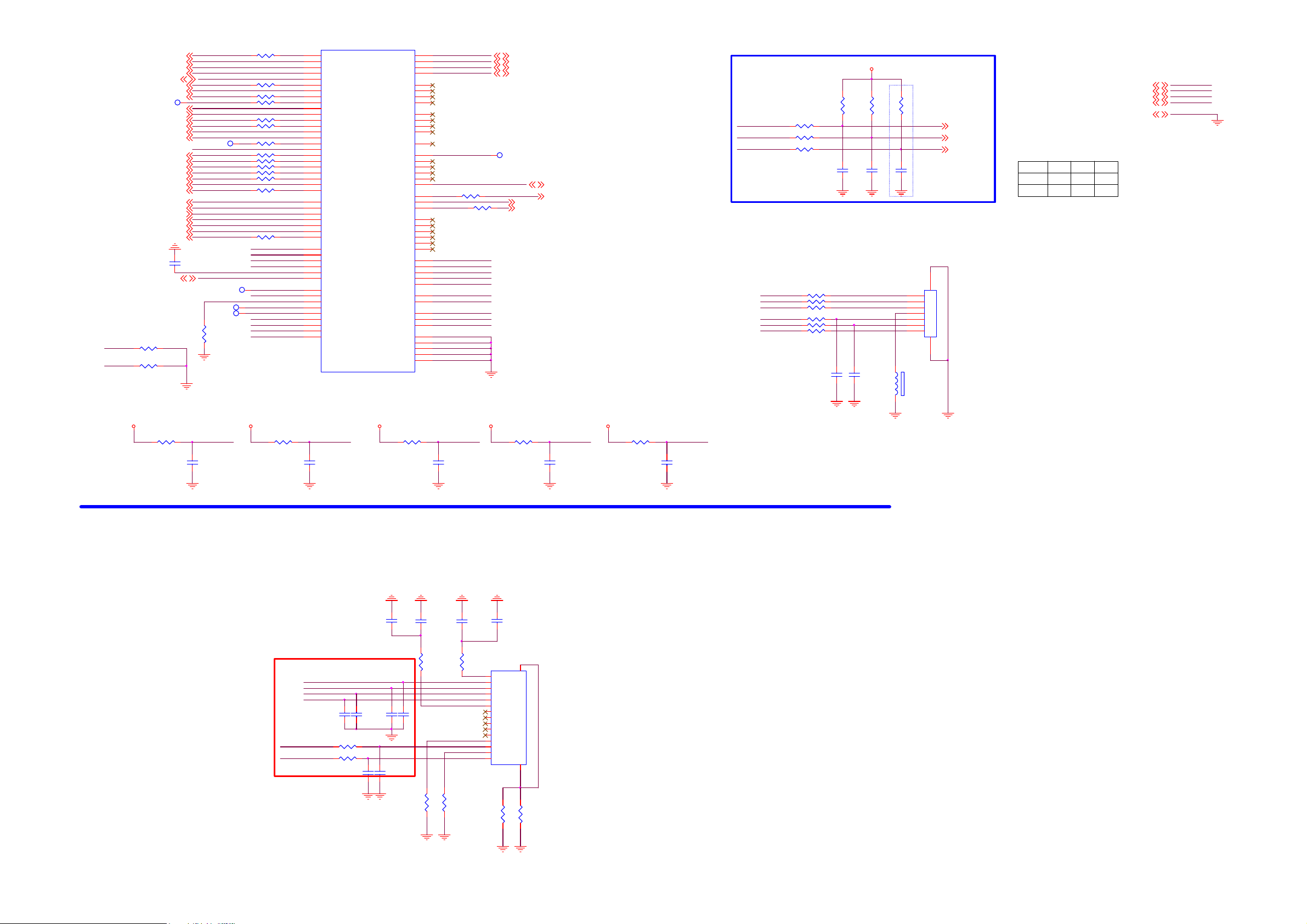
13 MII/GPIO/ServAD
ADIN 1
ADIN 0
USB_PWR _EN015
VGA_EEPROM_WP8
HDMI_SW_I2C12
PW_ERROR4
LVDSI 2C_ON9
TP41 1
Panel I2C_READY9
Panel ROM_WP9
AMP_RESETN6
Panel PE9
LVDS_PWR_EN4, 9
Panel VCC_DET9
Panel L/R_REF9
SYS_EE PROM_WP3
Panel IR_VSY NC9
C4133
100N 16V
USB_OC_COM15
R4125
10K 1/16W
R4148
10K 1/16W
LC-32SV502B/LC-42SV502B/LC-42SV602B/LC-46SV602B/LC-46SV502L
U401-9
AH7
AH10
AK8
AD27
AD28
N27
N28
N29
D32
D30
C30
D29
C29
C32
C31
AE14
AG12
AJ11
AH12
AK12
AJ12
AF12
AG17
AG16
AF17
AF18
AH17
AF19
AA28
AB28
AA32
AF32
AF31
AD31
AD32
AE31
AE32
AK6
AJ6
AK7
AJ8
L29
K30
L28
E29
E30
GPIO0
GPIO1
GPIO2
GPIO3
GPIO4
GPIO5
GPIO6
GPIO7
GPIO8
GPIO9
GPIO10
GPIO11
GPIO12
GPIO13
GPIO14
GPIO15
GPIO16
GPIO17
GPIO18
GPIO19
GPIO20
GPIO21
GPIO22
GPIO23
OPCTRL0
OPCTRL1
OPCTRL2
OPCTRL3
OPCTRL4
OPCTRL5
OPCTRL6
ADIN 0_SRV
ADIN 1_SRV
ADIN 2_SRV
ADIN 3_SRV
ADIN 4_SRV
ADIN 5_SRV
PHY LED1
PHY LED0
REXT
TAN A_1
TAN A_0
TXVN_ 1
TXVP_1
TXVN_ 0
TXVP_0
MT5395LPOJ
DEMOD_TSCLK
DEMOD_TSVAL
DEMOD_TSSY NC
DEMOD_TSDATA0
CI_TSSYNC
CI_TSD ATA0
PVR_TSCLK
PVR_TSVAL
PVR_TSSY NC
PVR_TSDATA0
PVR_TSDATA1
DEMOD_RST
LDM_VSY NC
AVDD12_REC
AVDD12_COM
AVDD33_COM
AVDD33_REC
AVDD3 3_LD
AVSS12_REC
AVSS12_COM
AVSS33_COM
AVSS33_REC
AVSS33_LD
USB_PWR_EN 0
VGA_EEPROM_WP
LED_G3
VGA_SW8
GPIO79
ALL_Mute6
HP_DET#5
Amp_Mute6
3D_SW9
LED_R3
pass_ through3
AC_DET4
BL_ON/OFF4
OPCTRL43
OPCTRL53
ARC_OE12
LED_G
LVDSI2C_ON
VGA_SW
ALL_Mute
Panel I2C _READY
Panel ROM_WP
Amp_Mute
AMP_RESETN
TP41 2
DE
Panel PE
LVDS_PW R_EN
3D_SW
SYS_EE PROM_WP
Panel IR _VSYN C
LED_R
BL_ON/OFF
OPCTRL4
OPCTRL5
ARC_OE
R4134 0R05 1/16W
PW_ERROR
R4153 0R05 1/16W
GPIO7
R4154 0R05 1/16W
R4155
NC/0R05 1/16W
R4156 0R05 1/16W
R4157 0R05 1/16W
R4171 NC/0R05 1/16W
R4160 0R05 1/16W
R4161 0R05 1/16W
R4162 0R05 1/16W
R4163 0R05 1/16W
R4164 0R05 1/16W
R4165 0R05 1/16W
R4158 0R05 1/16W
ADIN 0
ADIN 1
KEY_UP_D N
KEY_MENU
LIGHT_SENSOR
USB_OC_ COM
LED2/ PHYAD2
TP40 8
REXT
TP40 9
TP41 0
R4120
24K OHM + -1% 1/10W
LED3/ PHYAD3
TAN A_1
TAN A_0
MDI _TN
MDI _TP
MDI _RN
MDI _RP
CI_TSCLK
CI_TSVAL
SPI_CL K1
SPI_CLK
SPI_DATA
SPI_CLE
CI_INT
OPWM2
OPWM1
OPWM0
SD_D0
SD_D1
SD_D2
SD_D3
SD_CMD
SD_CLK
LDM_CS
LDM_CLK
LDM_DO
LDM_DI
U32
V29
V30
U30
U29
T27
U28
T29
R29
T28
R28
R31
R32
P30
P31
P32
P28
P29
U31
AA27
AC32
AA26
N32
M30
L30
L31
N31
N30
E32
E31
F32
D31
F30
AE30
AD30
AC27
AC28
AC29
AF29
W23
AG28
W22
V22
DEMOD_TSCLK
DEMOD_TSVAL
DEMOD_TSSY NC
DEMOD_TSDATA0
SPI_CL K1
DEMOD_RST
R4176
10K 1/16W
OPWM1
LDM_HSYN C
LDM_CS
LDM_CLK
LDM_VSY NC
LDM_DO
LDM_DI
AVDD12_REC
AVDD12_COM
AVDD33_COM
AVDD33_REC
AVDD33_LD
AVSS12_REC
AVSS12_COM
AVSS33_COM
AVSS33_REC
AVSS33_LD
R4152
0R05 1/16W
DEMOD_TSCLK 16
DEMOD_TSVAL 16
DEMOD_TSSY NC 16
DEMOD_TSDATA0 16
TP40 5
3D_IR_PU LSE
DEMOD_RST 16,17
3D_IR _PULSE 3
OPWM1 4
LVDS_f ormat 4,9
KEY_U P_DN
KEY_MENU
LIGHT_SEN SOR
LDM_VSY NC
LDM_HSY NC
LDM_CS
LDM_DO
LDM_CLK
LDM_DI
R4111
2K2 +-1% 1/16W
R4112
R4116 0R05 1/16W
R4117 0R05 1/16W
R4167 0R05 1/16W
2K2 +-1% 1/16W
C4112
100N 16V
TO KEY PAD BOARD
R4109 NC/47 OHM 1/16W
R4147 NC/47 OHM 1/16W
R4110 NC/47 OHM 1/16W
R4113 NC/47 OHM 1/16W
R4114 NC/47 OHM 1/16W
R4115 NC/47 OHM 1/16W
C4110
C4111
NC/100N 16V
NC/100N 16V
+3V3SB
C4113
100N 16V
R4168
10K 1%
C4135
100N 16V
NC/CONN
12
Key _POW
CN405
1
2
3
4
5
6
7
FB404
NC/ 220R
Key 1
Key 2
89
Key 1 3
Key 2 3
Key _POW 3
In-house
ODM
AVDD3V34, 7,9,12
DVDD3V33,4,5, 6,9,12,15,16, 17
+3V3SB3,4,12
AVDD1V23,4,7, 9,10,12,16
GND3,4,5, 6,7,8, 9,10,11,12, 14,15,16,1 7
R4168R4112R4111
10K10K10K
NC2. 2K2.2K
R4118
0R05 1/10W
AVDD33_LD AVDD12_COM AVDD12_R EC AVDD 33_REC AVDD33_COM
C4114
100N 16V
R4119
0R05 1/10W
C4109
100N 16V
MII ETHERNET PHY
Modified by EMI
MDI _TP
MDI _TN
MDI _R P
MDI _R N
NC/ 10PF 50V
LED3/ PHYAD3
DE
R4187 0R05 1/16W
R4188 0R05 1/16W
C4158
NC/ 10PF 50V
NC/ 10PF 50V
C4159
NC/ 10PF 50V
C4162
R4121
0R05 1/10W
C4160
C4163
NC/ 10PF 50V
C4125
10NF 50V
0R05 1/10W
C4161
NC/10PF 50V
C4123
100N 16V
R4132
C4115
100N 16V
C4122
100N 16V
R4133
0R05 1/10W
1
2
3
4
5
6
7
8
9
10
11
12
13
14
15
R4122
0R05 1/10W
TCT P 1
TD+ P2
TD- P3
RD+ P4
RD- P5
RCT P6
NC P7
NC P8
NC P9
NC P10
NC P11
Y- P12
Y+ P13
G- P14
G+ P15
C4124
10NF 50V
16
TH1
TH2
17
C4116
100N 16V
CN406
NC/RJ45 CONN+LED 15P
Act ivit y LE D: Yell ow
Link LED: Green
Ethernet DTE Device
RJ45
AVDD3V3AVDD3V3 AVDD1V2AVDD1V2 AVDD3V3
R4123
0R05 1/ 10W
C4117
100N 16V
LINKED IN 100BT/ACT(BLINKING)
R4129 330OHM 1/10W
R4130 330OHM 1/10W
R4141
0R05 1/10W
SEPARATE GROUND
R4142
0R05 1/10W
87
Page 88

LC-32SV502B/LC-42SV502B/LC-42SV602B/LC-46SV602B/LC-46SV502L
14 GND
AA14
AD3
AD4
R11
U11
AA16
AA20
T12
AA18
AB12
W19
Y19
AB21
N20
R20
U20
V20
W20
M13
AB20
M15
R21
W21
AA21
N13
P13
R13
T13
U13
V13
W13
Y13
AA13
N14
P14
R14
T14
U14
V14
W14
Y14
U12
N15
P15
AF28
AF25
AE26
AE27
F28
L27
AD26
AE25
AB11
AB14
L11
M11
P20
R12
L15
DVSS
DVSS
DVSS
DVSS
DVSS
DVSS
DVSS
DVSS
DVSS
DVSS
DVSS
DVSS
DVSS
DVSS
DVSS
DVSS
DVSS
DVSS
DVSS
DVSS
DVSS
DVSS
DVSS
DVSS
DVSS
DVSS
DVSS
DVSS
DVSS
DVSS
DVSS
DVSS
DVSS
DVSS
DVSS
DVSS
DVSS
DVSS
DVSS
DVSS
DVSS
DVSS
DVSS
DVSS
DVSS
DVSS
DVSS
DVSS
DVSS
DVSS
DVSS
DVSS
DVSS
DVSS
DVSS
DVSS
DVSS
DVSS
DVSS
U401-10
DVSS
DVSS
DVSS
DVSS
DVSS
DVSS
DVSS
DVSS
DVSS
DVSS
DVSS
DVSS
DVSS
DVSS
DVSS
DVSS
DVSS
DVSS
DVSS
DVSS
DVSS
DVSS
DVSS
DVSS
DVSS
DVSS
DVSS
DVSS
DVSS
DVSS
DVSS
DVSS
DVSS
DVSS
DVSS
DVSS
DVSS
DVSS
DVSS
DVSS
DVSS
DVSS
DVSS
DVSS
DVSS
DVSS
DVSS
DVSS
DVSS
DVSS
DVSS
DVSS
DVSS
DVSS
DVSS
DVSS
DVSS
DVSS
V19
U19
T19
R19
P19
N19
V21
Y18
W18
V18
U18
T18
R18
P18
L13
R27
R26
W12
N18
Y17
W17
V17
U17
T17
R17
P17
N17
AB16
Y16
W16
V16
U16
T16
R16
P16
N16
M16
Y15
W15
V15
U15
T15
R15
AF26
AF27
AG27
AK32
M19
AK31
AK30
AH28
AF16
AG26
AH27
AF8
AH29
W11
U21
GND 3,4,5,6,7,8,9,10,11,12,13,15,16,17
MT5395LPOJ
88
Page 89

15 USB
LC-32SV502B/LC-42SV502B/LC-42SV602B/LC-46SV602B/LC-46SV502L
GND3,4,5,6, 7,8, 9,10,11,12,13,14,16, 17
DVDD3V3
R1103
10K 1/10W
USB_OC_C OM
R1136
10K 1/10W
USB PORT 1
USB_PWR_EN0
HI = > POWER ON
LO = > POWER OFF
R1108
4.7K1/16W
+5V_U SB
For improved EMI, consider us ing a differential line filter
USB_PWR_EN013
USB_PWR_EN0
designed for USB applications. (e.g. TDK
ACM2012-900)
CN106
L118 90 ohm
USB_DP1
USB_DM1
1 2
U107
4
IN
1
EN
GND
2
5
OUT
3
OC
G5250K1T1U
+
C1118
220UF 16V
C1113
100N 16V
FB113
120R/3000mA
1
2
4
3
12
ZD132
VPORT0603100KV05
USB0_VBUS
12
ZD131
VPORT0603100KV05
65
4
3
2
1234
1
USB CONN
USB_OC_COM13
USB_DP09
USB_DM09
USB_DP19
USB_DM19
+5V_U SB4
DVDD3V33,4,5,6, 9,12, 16,17
+5V_SW4,5,6,9,11,12,16,17
AVDD1V23,4,7, 9,10,12,13,16
USB_OC_C OM
USB_DP0
USB_DM0
USB_DP1
USB_DM1
USB PORT 2
DVDD3V3
12
FB107
NC/120R/500mA
C144
NC/100N 16V
USB_DM0
USB_DP0
FOR WIRELESS
INTERNET
R119 NC/0R05 1/16W
R120 NC/0R05 1/16W
1
2
3
4
CN102
56
NC/CONN
For improved EMI, consider us ing a differential line filter
designed for USB applications. (e.g. TDK
ACM2012-900)
L115 90 ohm
USB_DP0
USB_DM0
1 2
FB117
120R/3000mA
1
2
4
3
12
12
ZD105
VPORT0603100KV05
USB1_VBUS
ZD107
VPORT0603100KV05
CN107
65
4
3
2
1234
1
USB CONN
89
Page 90

LC-32SV502B/LC-42SV502B/LC-42SV602B/LC-46SV602B/LC-46SV502L
16 ISDB-01 Demod
External ISDB Demod
Close to TUNER
C1132
FAT_IN+
FAT_IN-
1uF 25V
C1133
1uF 25V
Close to ISDB-T Demod
C1134
R1122
47 OHM 1/16W
R1123
47 OHM 1/16W
82pF 50V
C1135
82pF 50V
+2V5_DEMOD
+2V5_DEMOD
+1V2_DEMOD
R1124
47 OHM 1/16W
R1125
47 OHM 1/16W
R160
NC/ 0R05 1/16W
TUNER_DATA
TUNER_CLK
IF_AGC _DEMOD
C161
100N 16V
C160
100N 16V
37
38
39
40
41
42
43
44
45
46
47
48
49
C166
18P 50V
+2V5_DEMOD
C180
100N 16V
TAI NM
TAI NP
TAVS S
TAVD D
SLVADR1
XTA LS E L
VSS3
CVDD4
TTUS DA
TTUS CL
GPIO1
TIF AGC
E-Pad
36
1
1
XVSS
GPIO0
24
35
XTALI
GPIO22TSSYNC
X10 1
41.0MHz
3
R156
470R 1/10W 1%
+1V2_ADEMOD
100N 16V
34
32
33
XVDD
XTALO
TSVALID4TSCLK
5
3
C181
PVDD
C165
18P 50V
30
31
PVSS
6
C159
100N 16V
NC/10K 1/16W
+1V2_DEMOD
100N 16V
DEMOD_RST
29
RST_X
OSCMOD E
28
R126
C175
27
CVDD3
DVDD3V3
26
CVSS3
OSCEN_X
CVDD110TSDATA19TSDATA08DVDD17VSS1
11
C176
100N 16V
C117
NC/ 100N 16V
R161
0R05 1/16W
25
SLVADR0
TESTMOD E
CVSS2
CVDD2
DVDD2
VSS2
TSD ATA7
TSD ATA6
TSD ATA5
TSD ATA4
TSD ATA3
TSDATA212CVSS1
U101
CXD2828ER
SDA
SCL
DVDD3V33,4,5,6,9, 12,15,17
GND3,4, 5,6,7,8,9, 10,11,12,13, 14,15,17
DAC_3V34,5
AVDD1V23,4,7, 9,10,12,13
+5V_SW4,5,6, 9,11,12,17
IF_AGC _DEMOD17
FAT_IN+17
FAT_IN-17
TUNER_CLK17
TUNER_DATA17
T_OS DA7
T_OS CL7
DEMOD_RST13, 17
DEMOD_TSCLK13
DEMOD_TSVAL13
DEMOD_TSSYNC13
DEMOD_TSDATA013
24
23
22
21
20
19
18
17
16
15
14
13
T_OS DA
T_OS CL
C177
100N 16V
R1133
4.7K 1/10W
R1135
4.7K 1/10W
C179
100N 16V
R159
22R 1/10W 5%
R162
22R 1/10W 5%
+1V2_DEMOD
C178
NC/ 10P 50V
SMD/0402
+3V3_DEMOD
FB111
60 OHM
DEMOD_TSDATA0
12
DEMOD_TSCLK
C152
10PF 50V
SMD/0402
IF_AGC _DEMOD
FAT_IN+
FAT_IN-
TUNER_CLK
TUNER_DATA
T_OS DA
T_OS CL
DEMOD_RST
DEMOD_TSCLK
DEMOD_TSVAL
DEMOD_TSSYNC
DEMOD_TSDATA0
CXD2828ER Reserved LDO Power
+5V_SW
L110
1 2
120R/3000m A
C1128
10uF 10V
C1129
0.1uF 50V
U106
VIN3VOUT
GND14
AVDD1V2
DAC_3V3
2
4
L103
1 2
120R/3000m A
L117
1 2
120R/3000m A
L108
1 2
120R/3000m A
+
C1130
100UF 16V
+3V3_DEMOD
C1131
0.1uF 50V
C164
10uF 10V
C163
10uF 10V
C168
10uF 10V
+1V2_DEMOD
L109
1 2
120R/3000m A
L112
1 2
120R/3000m A
+1V2_DEMOD
+1V2_AD EMOD
+3V3_DEMOD
+2.5V _TUNER
+2V5_DEMOD
+2V5_DEMOD
R157 22R 1/10W 5%
R158 22R 1/10W 5%
DEMOD_TSVAL
DEMOD_TSSYNC
90
Page 91

17 ATSC-02-Tuner
TU 102
NC/SUT-RA217
I2C_SCL
I2C_SDA
RESET
TH18TH29TH310TH411TH5
12
IF_P
IF_N
AGC
A2.5V
1
2
3
4
5
6
7
DIF1
DIF2
IF_AGC_T
SCL
SDA
DEMOD_RST
+2.5V_TUN ER
Close to TUNER
IF_AGC_T
C1136
10N 50V
SMD/0402
C1138
10N 50V
SMD/0402
R1126
4.7K 1/16W
SMD/0402
R1129
4.7K 1/16W
SMD/0402
ITEM SUT-RB211
22K 1/16W
R1128
NC/0R05 OHM
R1127
R1129
C1138
R1128 Y
R1127 NY
R107
R109
Close to ISDB-T Demod
10K 1/16W 5%
R1130
22K 1/16W
C1139
100N 16V
R1131
Y
Y
N
N
N
IF_AGCT
SUT-RA217
IF_AGC_DEMODIF1_AGC_DEMOD
LC-32SV502B/LC-42SV502B/LC-42SV602B/LC-46SV602B/LC-46SV502L
DVDD3V33,4,5,6, 9,12, 15,16
GND3,4,5,6, 7,8, 9,10,11,12,13,14,15, 16
+5V_SW4,5,6,9, 11,12, 16
To/From MT5395
TU_FAT_IN 2+7
N
N
Y
Y
TU_FAT_IN 2-7
IF_AGCT7
IF_AGC_DEMOD16
FAT_IN+16
FAT_IN-16
TUNER_CLK16
TUNER_DATA16
DEMOD_RST13,16
TU_FAT_IN2+
TU_FAT_IN2-
IF_AGCT
To DEMOD
IF_AGC_DEMOD
FAT_IN+
FAT_IN-
TUNER_CLK
TUNER_DATA
DEMOD_RST
TU 101
SUT-RB211TV
TH3
TH4
TH5
TH6
13
14
15
16
17
IF1_P
IF1_N
AGC1
IF2_P
IF2_N
AGC2
I2C_SCL
I2C_SDA
2.5V
RESET
5V
TH1
TH2
12
R177
3.3K
DVDD3V3
R176
3.3K
TUNER_CLK
TUNER_DATA
Tuner I2C
SCL
C189
39P 50V
To guard for IF+/- signal
SDA
if cross over GND plane.
Layout dependant .
1
2
3
4
5
6
7
8
9
10
11
FAT_IN+
FAT_IN-
IF1_AGC_DEMOD
DIF1
DIF2
IF_AGC_T
SCL
SDA
DEMOD_RST
+5VTUN
R192
10K 1/10W
+2.5V_TUN ER
C183
10N 50V
C182
0.1uF 50V
FB112
1 2
120R/3000mA
C185
10uF 10V
+5V_SW
FAT_IN+
DIF1
DIF2
FAT_IN-
R107
NC/0R05 OHM
NC/47pF 50V
R109
NC/0R05 OHM
C1141
1uF 25V
C186
C187
NC/47pF 50V
C1142
1uF 25V
Close to tuner
R170
0R05 OHM
R171
0R05 OHM
C197
47pF 50V
C196
47pF 50V
C188
39P 50V
R117
100R 1/ 10W 5%
R118
100R 1/ 10W 5%
Clos e to M T5395
R174
100R 1/ 10W 5%
R175
100R 1/ 10W 5%
TU_FAT_IN2+
R140
150 OHM 1/10W
TU_FAT_IN2-
Impedance Contrl 100ohm and
route these path w ith differe ntia l
pattern on top layer.
91
Page 92

LC-32SV502B/LC-42SV502B/LC-42SV602B/LC-46SV602B/LC-46SV502L
[2] POWER SCHEMATIC DIAGRAM
!
SG9905
DSPL201M-A21F
R9904
NC
SG9903
DSPL201M-A21F
!
12
t
12
!
t
12
FB9805
BEAD
F9901
1 2
3 4
T6.3AH 250V
!
RV9903
TVR14561KFAOZF
HEAT SINK(BD9901)
R-
FB903
BEAD
1 2
HEAT
SINK(D8120,Q8101)
LED_CS
!
L9903
124
3
12MH
BOX
C9911
680NF 305V
change to 8.5mm
!
!
IC9901
NC
1
NC
NC
2
D1
D2
3
D1
D2
NC4NC
C9901
NC
C9906
220PF 250V
C9908
220PF 250V
!
L9901
3
124
12MH
R9901
750K
C9910
change to 8.5mm
680NF 305V
NR9902
NTCR
D145T60P7_5-1_2-R
!
NR9901
NTCR
D145T60P7_5-1_2-R
!
RV9901
TVR14102KJ200W
1 2
SG9901
SPARK GAP
NC
HS9901
1
2
3
4
HS9801
HEAT SINK
1
2
3
4
C9914
NC
HS9101
341
2
HEAT SINK
RV9902
R-
TVR14561KFAOZF
SG9904
!
DSPL201M-A21F
R9905
NC
8
7
!
6
5
C9907
220PF 250V
!!
!
SG9902
DSPL201M-A21F
!
!
!
CN901
AC SOKET
1
2
CN905
CONN
HEAT SINK(Q9801,D9801)
C9904
NC
HEAT
SINK(Q9101,Q9102)
4
CN904
CONN-NC
12
FB9806
BEAD
F9902
1 2
3 4
T6.3AH 250V
2
-
BD9901
3
TS10B06G-06-X0
1
2
L
N
R9805
200KOHM 1/8W +/- 5%
B1+
VCC1
100N 50V
C9162
C9145
100N 50V
100N 50V
R9146
2.43K +-1% 1/4W
+
R9164
NC
10K 1/8W
16K9 1/8W 1%
C9146
C9148
4.7UF 10V
1
1 2
R-
R2A20113A
IC9801
1
FB
2
COMP
3
RT
VREF4CS
R2A20113ASP
R9806
56K 1/8W
C9824
22N 50V
R9141
0R1 1W 1%
R9165
Q9104
NTD4906NT4G
R9145
!
HS9807
SHIELD
FB902
BEAD
VCC
OUT
GND
C9825
220N 50V
R9143
100 OHM 1/4W
VCC1
+
C9147
22UF 50V
R9147
470 OHM 1/8W
C9149
100N 50V
GDZJ30B
C9913
470PF 250V
1
2
3
C9820
1UF 450V
8
7
6
5
R9804
NC
R9142
1.5M 1% 1/4W
43
ZD9105
!
!
4
6
300UH
!
1 2
!
L9801
1
5
R9807
100 OHM 1/4W
12
C9826
NC
C9827
470PF 50V
1.5M 1% 1/4W
C9150
2.2UF
R9158
7.5K OHM 1%
12
IC9106
PC123X8YFZ OF
IC9107
AS431AZTR-E1
C9903
470PF 250V
!
C9831
2N2 50V
BZT52-B22
ZD9106
BZT52-B5V1
R9810
16K 1% 1/8W
NTD4906NT4G
R9150
1.5M 1% 1/4W
R9144
VBoot
B2+
D9802
IN5408G-10
D9801
FMN-1106S
VCC1
ZD9107
1 2
Q9802
C9151
1UF
C9152
10PF
R9148
NC
C9171
1UF 16V
FB9801
BEAD
1 2
10R 1/8W 5%
+
C9830
10UF 50V
R9811
100 OHM 1/4W
470 OHM 1/8W
C9154
560P 50V
24V
R9159
20K 1/4W
C9158
NC
C9159
330NF 50V
!
FB9802
1 2
BEAD
100N 50V
1
2
3
4
5
6
7
8
R9808
C9832
UF4007
D9114
R9149
C9172
FB9803
1 2
BEAD
C9828
100N 50V
C9829
100N 50V
R9817
100K +-1% 1/4W
IC9101
Vsen
Vcc
FB
GND
Css
OC
RC
Reg
RV9COM
SSC9512S-TL
C9153
1uF
R9160
10K OHM
2.2nF 630V
10K 1/8W
R9819
R9151
10 OHM
NC
NC
VGH
VS
VB
NC
NC
VGL
BZT52-B13
R9101
180R 1%
!
D9803
RB160M
R9809
30R +-1% 1/8W
10K OHM +-5% 1/8W
R9818
1K 1/4W
18
17
16
15
14
13
12
11
10
ZD9104
1 2
12V
C9915
470PF 250V
+
C9801
47UF 450V
12
R9813
R9816
R9815
680K OHM +-1% 1/4W
680K OHM +-1% 1/4W
D9113
RB160M
R9152
47OHM +-5% 1/8W
D9112
RB160M
R9154
47OHM +-5% 1/8W
10K 1/8W 1%
C9155
1N 50V
24V
R9161
24K 1/8W 1%
R9163
2K 1/8W 1%
C9905
470PF 250V
+
C9802
47UF 450V
Q9801
TK18A60V
!
R9801
0.05R
1MOHM +-5% 1/4W
R9814
VCC1
12
R9153
10K 1/8W 1%
12
R9155
C9156
100PF1KV
R9180
27Kohm 1/4W +/-1%
+
C9804
47UF 450V
R9102
10 OHM
R9103
10 OHM
+
C9805
47UF 450V
R-
B1+
!
!
HEAT SINK (D 9308)
1
2
3
4
1
2
3
4
Q9101
TK10A50D
Q9102
TK10A50D
HS9301
HS9103
HEAT SINK
B1+
R9329
0R1 5% 3W
C9803
470PF1KV
C9333
0.47UF 50V
R9317
1.5M 1% 1/4W
!
HEAT
SINK(D9115,D9116)
VBoot
VCC1
R9325
100K
R9326
100K
R9320
510K 1% 1/8W
R9318
1.5M 1% 1/4W
1
2
6
7
C9157
22NF 800V
+
C9302
22UF 50V
ZD9301
MTZJ18B
R9327
100K
R9328
100K
D9305
FR107
R9301
1.0R
R9319
1.5M 1% 1/4W
T9101
!
POWER X'FMR
VCC
Q9303
2SD1624T-TD-E
R9306
10K OHM
1 2
C9331
1NF
R9323
4.7M OHM +-5% 1/4W
!
1
S/OCP
2
BR
3
GND
FB/OLP4VCC
C9334
1N 50V
13
15
14
12
11
8
9
10
Main_ov
12
D9302
!
12
43
IC9302
R9302
100K
IC9301
A6069H
D/ST
D/ST
C9335
100N 50V
!
D9304
FR107
220R 1%
R9305
RB160M
PC123X8YFZ OF
8
7
5
3
1
D9306
1N4148
BOX
D9116
FMEN-2308
2
VCC
1
3
+
C9336
10UF 50V
D9115
FMEN-2308
2
1
2
3
5
4
R9332
2R2 +-5% 1/4W
D9307
FR107
+
C9337
47UF 50V
C9160
180UF 63V
DV5
R9178
5K1 +-5% 1/8W
Q9304
T9301
POWER X'FMR
ZD9303
MTZJ15B
1 2
GDZJ6. 2B
D9117
3
FMEN-2308
2
1
C9161
180UF 63V
+
+
C9168
330UF 25V
Q9305
MMBT3906 PNP
R9307
10K 1% 1/4W
NC
C9345
NC
!
6
7
9
10
ZD9103
FB9804
BEAD
1 2
43
1 2
24V
+
+
330UF 25V
R9308
10K 1/8W 1%
A
L9104
3UH
C9163
R9309
NC
R9310
NC
!
12
R9174
5.1K 1/4W
0 OHM 1/8W
R9330
47 OHM 1/4W
R9331
47 OHM 1/4W
D9308
1
FMW-2156
2
3
IC9303
PC123X8YFZ OF
IC9304
AS431AZTR-E1
L9106
3UH
C9166
+
470UF 25V
R9311
C9343
220N 50V
24VA
L9103
3UH
C9165
100N 50V
A
Q9302
PMBS3904
1NF
C9338
+
R9334
220 OHM
R9335
3K3 1/8W 5%
1K 1/8W 1%
+24V
C9301
100N 50V
C9344
470UF 10V
R9337
8K2 1/8W 1%
R9336
R9338
12K 1/8W 1%
L9105
3UH
change to 150uF
+
C9169
330UF 25V
R9304
100K 1/8W 1%
A
+
20K 1/8W 1%
C9164
180UF 63V
22K 1%
R9303
C9340
330UF 25V
R9339
+
L9304
3UH
Q9301
R9341
100K 1/8W 1%
R9175
1.5K 1/4W
PS-On
RK7002BM
R9171
5.1K 1/4W
R9176
1.5K 1/4W
Main_ov
+
C9341
330UF 25V
1 2
24VA
R9340
10K 1/8W 1%
R9172
5.1K 1/4W
R9177
1.5K 1/4W
D9301
RB160M
12V_LED
P_OK
12V
PS-On
5.2V
P_OK
DIM
On/Of f
C9342
100N 50V
DV5
R9173
5.1K 1/4W
+24V
DIM
C9170
100N 50V
R9333
1K 1/8W 1%
Q9103
PMBS3904
1K 1/8W 1%
On/Of f
5.2V
R9138
P_OK
On/Of f
15
14
13
12
11
10
9
8
7
6
5
4
3
2
1
CN902
13
12
11
10
9
8
7
6
5
4
3
2
1
CONN
12V
5.2V
CN903
CONN
24V-LED
R9343
NC
R9345
0 OHM 1/4W
R9111
NC
R9324
1K 1/8W 1%
Q9106
MMBT3906 PNP
C9144
100N 50V
24VA
13
12
11
10
9
8
7
6
5
4
3
2
1
1 2
15
14
13
12
11
10
9
8
7
6
5
4
3
2
1
CN907
CONN-NC
ZD9101
MTZJ30B
D9109
1N4148
5.2V
NC
CN906
Wire Harness
R9342
12V
ZD9102
MTZJ15B
1 2
D9110
1N4148
R9139
100 OHM 1%
R9140
1K 1/8W 1%
EN
92
Page 93

24V-LED
1
L8101
25UH
LC-32SV502B/LC-42SV502B/LC-42SV602B/LC-46SV602B/LC-46SV502L
1
2
Q8101
3
D8120
MBRF10150CT
TK12A10K3
2
R8145
220K +-1% 1/4W
C8118
100UF 100V
R8147
12K 1/8W 1%
VLED
R8154
+
C8108
+
100UF 100V
100K
R8155
100K
R8156
100K
12V_LED
12V
R8177
NC
R8176
0R051/8W
ZD8103
BZT52-B13
1 2
1uF
C8124
1uF
C8123
LED_CS
1uF
C8122
C8111
100N 50V
22UF 50V
C8121
8
+
R8163
200K 1%
R8175
0.05R
IC8103
5
6
DIM
OUT7VCC
GND
FB1GM2RT3CS
4
C8105
1N 50V
PF7900S
R8157
10K 1/8W 1%
R8162
1K 1/8W 1%
R8153
0 OHM 1/4W
R8148
1K 1/8W 1%
C8119
NC
C8113
1N 50V
R8161
2.2 OHM 1/8W
R8158
12
22 OHM 1/8W
D8118
RB160M
DIM
C8106
NC
R8144
91KOHM +-1% 1/8W
R8141
20K 1% 1/8W
On/Of f
LED-COMP
12V
R9321
5K1 1%
C9346
NC
R9316
0 OHM +-5% 1/8W
R9313
NC
R9322
NC
Q9306
NC
R9312
NC
Q9308
NC
12V_LED
R9344
10K 1/8W
EN
R9315
3.9K1% 1/8W
93
Page 94

LC-32SV502B/LC-42SV502B/LC-42SV602B/LC-46SV602B/LC-46SV502L
IC8501
12V_LED
C8158
NC
EN
DIM
LED-1
+
1
DIM
2
EN
3
VCC
LED4GND
C8517
100N 50V
PF7700S
COMP
GM
ISET
8
7
6
5
5K6 +-1% 1/8W
R8501
LED-COMP
C8501
1UF 16V
IC8502
DIM DIM
EN
12V_LED
LED-6
1
DIM
2
EN
3
VCC
LED4GND
C8523
100N 50V
PF7700S
COMP
GM
ISET
8
7
6
5
5K6 +-1% 1/8W
R8502
LED-COMP
C8502
1UF 16V
EN
12V_LED
LED-2
IC8503
1
DIM
2
EN
3
VCC
LED4GND
PF7700S
C8529
100N 50V
COMP
GM
ISET
8
7
6
5
LED-COMP
R8503
5K6 +-1% 1/8W
C8503
1UF 16V
EN
12V_LED
LED-5
EN
12V_LED
LED-8
EN
12V_LED
LED-15
DIM
EN
12V_LED
LED-9
DIM
EN
12V_LED
LED-11
DIM
DIM
DIM
1
DIM
2
EN
3
VCC
LED4GND
PF7700S
C8518
100N 50V
1
DIM
2
EN
3
VCC
LED4GND
C8519
100N 50V
1
DIM
2
FLAG
3
VCC
LED4GND
NC
C8520
NC
1
DIM
2
FLAG
3
VCC
LED4GND
C8521
NC
1
DIM
2
FLAG
3
VCC
LED4GND
NC
C8522
NC
IC8504
COMP
GM
ISET
IC8507
COMP
GM
ISET
PF7700S
IC8510
COMP
GM
ISET
IC8513
COMP
GM
ISET
NC
IC8515
COMP
GM
ISET
8
7
6
5
5K6 +-1% 1/8W
8
7
6
5
R8507
5K6 +-1% 1/8W
8
7
6
5
R8510
NC
8
7
6
5
R8513
NC
8
7
6
5
R8515
NC
LED-COMP
R8504
LED-COMP
LED-COMP
LED-COMP
LED-COMP
C8513
NC
C8504
1UF 16V
C8507
1UF 16V
C8510
NC
C8515
NC
IC8505
DIM
EN
12V_LED
LED-3
DIM
EN
12V_LED
LED-7
DIM
EN
12V_LED 12V_LED
LED-12
DIM
EN
12V_LED
LED-10
DIM
EN
12V_LED
LED-13
1
DIM
2
EN
3
VCC
LED4GND
C8524
100N 50V
IC8508
1
DIM
2
EN
3
VCC
LED4GND
C8525
100N 50V
IC8511
1
DIM
2
FLAG
3
VCC
LED4GND
NC
C8526
NC
IC8514
1
DIM
2
FLAG
3
VCC
LED4GND
C8527
NC
IC8516
1
DIM
2
FLAG
3
VCC
LED4GND
C8528
NC
PF7700S
PF7700S
NC
NC
COMP
GM
ISET
COMP
GM
ISET
COMP
GM
ISET
COMP
GM
ISET
COMP
GM
ISET
8
7
6
5
5K6 +-1% 1/8W
8
7
6
5
5K6 +-1% 1/8W
8
7
6
5
8
7
6
5
8
7
6
5
LED-COMP
R8505
LED-COMP
R8508
LED-COMP DIM
R8511
NC
LED-COMP
R8514
NC
LED-COMP
R8516
NC
C8505
1UF 16V
C8508
1UF 16V
C8511
NC
C8514
NC
C8516
NC
LED-9
LED-10
LED-11
LED-12
LED-13
LED-14
LED-15
LED-16
VLED
VLED
12V_LED
DIM
EN
12V_LED
LED-4
DIM
EN
LED-14
EN
LED-16
12
11
10
9
8
7
6
5
4
3
2
1
CN8502
NC
1
DIM
2
EN
3
VCC
LED4GND
PF7700S
C8530
100N 50V
1
DIM
2
FLAG
3
VCC
LED4GND
C8531
NC
1
DIM
2
FLAG
3
VCC
LED4GND
C8532
NC
IC8506
COMP
ISET
IC8509
COMP
ISET
NC
IC8512
COMP
ISET
NC
LED-1
LED-2
LED-3
LED-4
LED-5
LED-6
LED-7
LED-8
GM
GM
GM
8
7
6
5
5K6 +-1% 1/8W
8
7
6
5
8
7
6
5
VLED
VLED
R8506
R8509
NC
R8512
NC
LED-COMP
LED-COMP
LED-COMP
CN8501
12
11
10
9
8
7
6
5
4
3
2
1
CONN
C8506
1UF 16V
C8509
NC
C8512
NC
LED-10
LED-9
LED-11
LED-8
LED-12
LED-7
VLED
VLED
LED-1
LED-6
LED-2
LED-5
LED-3
LED-4
瞷 ノ 尿 穝
1
2
3
4
5
6
7
8
1
2
3
4
5
6
7
8
CN8503
NC
CN8504
NC
94
Page 95

Only for LC-322SV502B
腹
LC-32SV502B/LC-42SV502B/LC-42SV602B/LC-46SV602B/LC-46SV502L
砰Θ
!
F9902
T6.3AH 250V
!
CN9901
AC SOKET
1 2
!
F9901
T6.3AH 250V
1 2
3 4
RV9902
TVR14561KFAOZ F-N C
387G050147F0ST
34
12
NR9902
1 2
NTCR
!
RV9901
TVR14561KFAOZ F
!
SG9905
DA38-622MT-A21F-NC
R9906
1MOHM +-5% 1/2W-NC
NR9901
1 2
NTCR
!!
t
1
2
3
!
t
SG9906
DA38-622MT-A21F-NC
!
R9904
510K-NC
IC9901
CAP004DG-NC
NC
D1
D1
NC4NC
C9903 47PF-NC
!
!
NC
D2
D2
R9901
510K-NC
8
7
6
5
!
R9903
220K 1/4W
R9902
220K 1/4W
R9905
220K 1/4W
!
!
!
!
C9902
220NF
SG9901
DSPL201M-A21F-NC
L9901
4
1
3
2
!
12MH
2
1
L
N
!
CN9902
CONN-NC
HOT
!
C9905
470PF 250V
COLD
!
C9904
470PF 250V
SG9902
DSPL201M-A21F
C9911
!
!
470PF 250V
!
C9901
220NF
SG9903
DSPL201M-A21F
L9902
4
1
12MH
SG9904
DSPL201M-A21F-NC
!
3
2
RV9903
TVR14561KFAOZ F
FB9901
1 2
BEAD
!
4
FB9902
BEAD
BD9901
3
KBJ608G-FU
FB9906
!
1 2
-
2
12
BO
1
+
BEAD
C9906
47UF 450V
! !
+
C9909
47UF 450V
+
C9907
47UF 450V
!
+
C9913
47UF 450V
!
+
B+
C9912
10NF
HS9901
1
2
3
4
HEAT SINK-NC
HS9902
1
2
3
4
HEAT SINK-NC
HS9101
1
2
3
4
HEAT SINK
12
HS9102
1
2
3
4
HEAT SINK
FB9302
BEAD
HS9302
1
2
3
4
HEAT SINK
C9908
470PF 250V
!
T P V ( Top Victory Electronics Co . , Ltd. )
絬隔瓜絪腹
Key Component
Date
Sunday , April 01, 2012
C9910
470PF 250V
!
OEM MOD EL
TPV MO DEL
PCB NAME
Sheet
715G5194-P01-W22-0020
41
of
Size
Rev
称爹
32,37 inch
95
Page 96

LC-32SV502B/LC-42SV502B/LC-42SV602B/LC-46SV602B/LC-46SV502L
J901
JUMPER
1 2
J916
JUMPER
1 2
J902
JUMPER
1 2
J917
JUMPER
1 2
J903
JUMPER
1 2
J918
JUMPER
1 2
J904
JUMPER
1 2
J919
JUMPER
1 2
J920
JUMPER
1 2
J950
JUMPER
1 2
J921
JUMPER
1 2
J951
JUMPER
1 2
J907
JUMPER
1 2
J922
JUMPER
1 2
J952
JUMPER
1 2
J908
JUMPER
1 2
J923
JUMPER
1 2
J953
JUMPER
1 2
J909
JUMPER
1 2
J924
JUMPER
1 2
J954
JUMPER
1 2
J910
JUMPER
1 2
J925
JUMPER
1 2
J955
JUMPER
1 2
J911
JUMPER
1 2
J926
JUMPER
1 2
J956
JUMPER
1 2
J912
JUMPER
1 2
J927
JUMPER
1 2
J957
JUMPER
1 2
J928
JUMPER
1 2
J958
JUMPER
1 2
J929
JUMPER
1 2
J959
JUMPER
1 2
J915
JUMPER
1 2
J960
JUMPER
1 2
RJ902
0R05 1/4W
CN9901-1
2.0MM RIVET
RJ903
0R05 1/4W
CN9901-2
2.0MM RIVET
1 2
J963
JUMPER
1 2
RJ904
0R05 1/4W
RJ914
0R05 1/4W
084G 34 14 084G 34 10
F9901-1
CQ-203SF
F9901-1
CQ-203SF
J964
JUMPER
┪
RJ907
0R05 1/4W
RJ917
0R05 1/4W
T9101-1
1.7MM RIVET
RJ908
0R05 1/4W
RJ919
0R05 1/4W
F9902-1
CQ-203SF-NC
F9902-1
CQ-203SF-NC
J967
JUMPER
1 2
T9101-2
1.7MM RIVET
1 2
RJ910
0R05 1/4W
J968
JUMPER
T9101-3
1.7MM RIVET
J969
JUMPER
1 2
GND1
GND TERMINAL
GND9
GND TERMINAL
T9101-4
1.7MM RIVET
GND11
GND TERMINAL
GND6
GND TERMINAL
GND10
GND TERMINAL
祏
GND7
GND TERMINAL
P09T0001 1
P09G0003 1
96
T P V ( Top Victory Electronics Co . , Ltd. )
絬隔瓜絪腹
Key Component
Date
Sunday , April 01, 2012
OEM MOD EL
TPV MOD EL
PCB NAME
Sheet
715G5194-P01-W22-0020
42
of
Size
Rev
称爹
32,37 inch
Page 97

2Mohm 1/4W +/ -1%-NC
2Mohm 1/4W +/-1%-NC
2Mohm 1/4W +/-1%-NC
Q9108
TK2P60D-NC
!
R9147
R9148
R9149
100N 50V-NC
R9150
2K 1/8W 1%
B+_main
C9132
R9129
0 OHM +-5% 1/8W
R9155
10K 1/8W
R9177
100KOHM +-5% 1/8W-N C
C9113
470NF 5 0V
VCC1
1
BNO
2
COMP
3
NC
CS4GND
C9128
1N 50V
B+_main
IC9103
OVP
VCC
OUT
LD7523GS
220 OHM 1/4W
R9112
!
8
7
6
5
C9114
100N 50V
C9108
10NF
R9111
10K OHM +-5% 1/8W
C9120
1.5NF
22OHM +-5% 1/8W
R9109
R9127
100R 1/8W 5%
C9134
1uF-NC
C9136
1uF-NC
C9135
1uF-NC
VCC1
!
R9113
100KOHM +-5% 2WS
D9101
PR1007
SS1060FL
D9104
12
R9110
10K OHM +-5% 1/8W
HOT
!
Q9101
TK6A65D
R9108
0.24 oHM 2W
COLD
!
T9101
8 9
6
5
1
POWER X'FMR
LC-32SV502B/LC-42SV502B/LC-42SV602B/LC-46SV602B/LC-46SV502L
R9157
R9104
R9103
R9105
3
1
R9182
24R 1%
R9181
24R 1%
R9153
24R 1%
R9152
24R 1%
R9154
24R 1%
C9104
D9102
FMEN210A
2
0 OHM 1/4W
R9183
0 OHM 1/4W
R9184
0 OHM 1/4W
+24V1
C9102
1.5NF
+
+
C9109
560UF 35V
C9103
1.5NF
C9106
470UF 35V
R9138
10 OHM 1/4W -NC
ZD9107
P6KE27A-NC
1 2
+
470UF 35 V
R9171
470R
Q9111
2SD1624T-TD-E
C9131
100N 50V
+12V
C9105
+12V1
+
ZD9106
MTZJ27B
1 2
R9172
1K 1/8W
R9176
3K 1/8W +/ -1%
+24V1
C9125
1N 50V
100K 1/8W
L9101
3UH
R9173
MMBT39 04
Q9107
AOD409
Q9112
C9107
270UF 25V
R9174
100K 1/8W
+
ZD9104
B6V2
1 2
R9175
1K OHM +-5% 1/8W
+12V
+24V1
C9112
0.47UF 50V
R9137
680 OHM 1/4W
R9156
680 OHM 1/4W
IC9105
AS431AN-E1
1.5K 1/4W
C9124
100N 50V
R9159
1.5K 1/4W
R9158
+24V2
+24V
R9151
1K OHM +-5% 1/8W
1.5K 1/4W
L9102
3UH
R9135
27K 1/8W 1%
R9136
3K 1/8W +/ -1%
R9161
1.5K 1/4W-NC
R916 0
C9101
220UF 3 5V
R9162
1.5K 1/4W-NC
+24V
+
R9180
10K 1/4W -NC
C9111
0.47UF 50V
+24V2
R9178
10K 1/4W- NC
+24V1
R9179
10K 1/4W-NC
100 OHM 1/4W
100 OHM 1/4W
100 OHM 1/4W
10
15
16
14
13
12
11
R9164
24R 1%
R9163
24R 1%
R9106
24R 1%
R9102
24R 1%
R9107
24R 1%
3
1
560UF 35V
+12V1
R9115
470OHM +-5% 1/8W
D9103
FMXA-2202S
2
FB9905
1 2
BEAD
C9129
1NF 25 0V-NC
!
C9122
470PF 250V
!
C9133
1NF 250V-N C
!
C9130
470PF 250V
!
Main power OVP latch circuit
5.2V
R9169
Q9102
2K OHM +-1% 1/8W
1K OHM +-5% 1/8W
R9168
Protect
D9108
SS1060F L
1 2
MMBT39 04
43
C9117
6.8nF
R9167
1K OHM +-5% 1/8W
Q9110
MMBT3906
12
IC9101
PC123X8YFZ OF
ZD9105
MTZJ 15B
1 2
4.7uF 25V
C9115
100NF 50V
!
2
C9110
SS1060F L
R9122
100 OHM +-1% 1/8W
R9121
1K OHM +1% 1/8W
3
D9105
1
+24V
R9114
3K 1/8W +/ -1%
D9107
BAV99
C9123
4.7uF 2 5V
ZD9102
MTZJ 30B
1 2
12
C9119
100N 50V
AS431AZTR-E1
IC9102
+12V
1 2
12
ZD9101
MTZJ 18B
D9106
SS1060F L
R910 1
5K1 1/8W 1%
VCC1
R9118
9K1 1/8W 1%
R9170
5.1K 1/4 W
R9117
1K8 +/-1% 1/8W
R9126
110R
VCC
C9118
4.7UF 50V-NC
R9116
120KOHM +-1% 1/8W
HOT
Q9103
2SD1624T-TD-E
+
R9124
2K 1/8W 1%-N C
R9123
2K 1/8W 5%
ZD9103
MTZJ18B
C9126
470NF 50V-N C
DV5
43
R9125
100KOHM +-5% 1/8W
1 2
C9127
470NF 50V -NC
R9128
200 OHM 1/4W
12
IC9104
PC123X8YFZ OF
Protect
!
R9139
10K 1/4W-NC
R9130
10K 1/4W
RK7002BM-NC
跋遏
10K 1/4W -NC
Q9106
PMBT3906 PNP
Q9105
2
R9140
10K 1/4W-N C
C9121
100N 50V-NC
R9141
R9142
10K 1/4W-NC
R9134
10K OHM +-5% 1/8W
5.2V
R9131
0 OHM +-5% 1/8W
R9132
20KOHM +-5% 1/8W-N C
Q9104
2N7002K
R9119
100KOHM +-5% 1/8W-N C
R9143
10K 1/4W-N C
5.2V
跋遏
R9144
10K 1/4W-NC
1
100N 50V
R9145
10K 1/4W- NC
㎝
42"
跋遏
1
跋遏
2
C9116
R9146
10K 1/4W-N C
R9165
10K 1/4W-NC
絬隔 ノ
3.3V 5V
X
O
X
O
R9133
20K +-5% 1/8W
R9120
100KOHM +-5% 1/8W
R9166
10K 1/4W- NC
PS_ON
97
T P V ( Top Victory Electronics Co . , Ltd. )
絬隔瓜絪腹
Key Component
Date
Sunday , April 01, 2012
OEM MO DE L
TPV MO DE L
PCB NAME
Sheet
715G5194-P01-W22-0020
43
of
Size
Rev
称爹
32,37 inch
Page 98

LC-32SV502B/LC-42SV502B/LC-42SV602B/LC-46SV602B/LC-46SV502L
FB9301
1 2
BEAD
B+
0.1R
R9302
BO
R9306
1.5M 1%
R9310
1.5M 1%
R9313
1.5M 1%
穦ノ蛮π蔼溃筿
C9310
220NF
C9312
10NF
D9301
1N4007
R9308
1.0R 1W
1.5M (1/4W)
R9317
560K 1/8W 1%
1.5NF
C9302
B+_main
1
2
3
C9308
1N 50V
5.2V->P6KE160A
3.3V->P6KE180A
!
D9304
PR1007
!
IC9301
S/OCP
D/ST
BR
D/ST
GND
FB/OLP4VCC
A6069H
R9315
4.7M 5% 1/8W
LAY
R9301
100KOHM +-5% 2WS-NC
12
ZD9315
P6KE160A
8
7
5
C9311
100N 50V
12
D9305
SS1060FL
3.3V
5.2V
!
+
腹
腹
R9305
2R2 +-5% 1/4W
D9303
PR1007
C9306
100UF 50V
!
+
C9309
10UF 50V
GDZJ5.6B
COLDHOT
080GL32P 89 F
080GL52P 48 YS
T93 01
1
!
2
3
5
4
POWER X'F MR
VCC
12
43
IC9302
PC123X8YF ZOF
!
IC9303
AS431AN-E1
ZD9316
1 2
R9319
47 OHM 1/4W
R9303
47 OHM 1/4W
R9304
47 OHM 1/4W
D9302
FMW-2156
6
7
9
10
3
1
D9308
1 2
SR240S-NC
R9312
1K OHM +-5% 1/8W
C9307
220N 50V
LAY 5VノD9302,3.3ノD9308
2
R9307
220R 1%
R9314
1K OHM +-5% 1/8W
STB 4.7V->5.2V
R9311-->061G08058201FT
R9316-->061G08059101FT
R9318-->061G08054302FT
STB 4.2V->5.2V
R9311-->061G08052401FT
R9316-->061G08053601FT
R9318-->061G08055601FT
output 3.3V
R9311-->061G08053601FT
R9316-->061G08052201FT
C9301
1.5NF
+
C9303
470UF 10V
R9311
2K4 +/-1% 1/8W
R9316
3K6 1/8W 1%
+24V
LAY
铬絬
5.2V
L9301
3UH
+
C9304
470UF 10V
+
C9313
270UF 25V
C9305
0.47UF 50V
GND_Audio
5V R9311->2.4K R9316->3.6K
3.3V R9311->3.6K R9316->2.2K
R9318
5K6 +-1% 1/8W
㎝
42"
絬隔 ノ
Q9301
2N7002K
10K OHM +-5% 1/8W
R9320
R9332
100KOHM +-5% 1/8W
SHARP
SJPW-T4VL-NC
DV5
ㄏノ
CN9303㎝CN9304
12
D9306
L9302
3UH-NC
5.2V
C9316
+
100UF 50V
R9309
10K 1/4W
ON/OFF
DIM
+12V
PS_ON
P_OK
PF7700 R9321㎝R9323 NC
PF7703 R9324 NC
R9321
0R05 1/4W-NC
P_OK
R9324
0 OHM +-5% 1/8W
ON/OFF
5.2V
R9323
10K 1/4W-NC
CN9303
12
12
11
11
10
10
9
9
8
8
7
7
6
6
5
5
4
4
3
3
2
2
1
1
Wire Harness
CN9302
13
13
12
12
11
11
10
10
9
9
8
8
7
7
6
6
5
5
4
4
3
3
2
2
1
1
CONN-NC
Wire Harness
EN
CN9301
CONN-NC
CN9304
C9314
470PF 250V
!
C9317
470PF 250V
!
98
T P V ( Top Victory Electronics C o . , Ltd. )
絬隔瓜絪腹
Key Component
Date
Sunday , April 01, 2012
OEM MOD EL
TPV MOD EL
PCB NAME
Sheet
715G5194-P01-W22-0020
44
of
Size
Rev
称爹
32,37 inc h
Page 99

[3] KEY SCHEMATIC DIAGRAM
C101
0.1uF 25V
VBIAS
U102
CIN_01
CIN_02
CIN_03
CIN_04
CIN_07
CIN_09
IT7235BFN -3108/AX (R)
1
CIN1
2
CIN2
3
CIN3
4
CIN4
5
CIN7
6
CIN9
OTP
GPIO_13
25
23
24
NC
THD1
E-PAD
CIN117VSHILD8VBIAS9AVSS10AVCC11GPIO11
CIN_11
AC_SHIELD
GPIO_02
VBIAS
GPIO_03
22
AVSS
DVSS
GPIO_04
19
20
DVSS
GPIO4
GPIO321GPIO2
GPIO7
SCLK
GPIO9
DVCC
12
3.3V
GPIO_11
C103
0.1uF 25V
INT#
SDA
LC-32SV502B/LC-42SV502B/LC-42SV602B/LC-46SV602B/LC-46SV502L
89
1
SM_SDA
SM_SCL
OTP
KEY2
3.3V
C105
0.1uF 25V
GPIO_07
18
17
SM_SDA
16
SM_SCL
15
GPIO_09
14
13
NC/ 2K2 1/ 16W 5%
3.3V
C102
0.1uF 25V
CH-
CH+
VOL
VOL
-
+
R122
2.94K 1%
GPIO_02
GPIO_11
GPIO_04
GPIO_13
R117
1.65K 1%
R121
820R 1%
330 OHM 1/16W
3.3V
R124
Key 1
R115
KEY1
CN0101
2
3
4
5
6
7
CONN
AC_shield is a large
cooper which encircles the
Cin button and it's path.
AC_SHIELD
1
Touch Pad Shieldelectrode
R112
100OHM1/16W
C104
100P 50V
MEN
INPUT
POWER
U
1.65K 1%
GPIO_09
GPIO_07
GPIO_03
R118
R119
820R 1%
3.3V
R116
NC/ 2K7 1/ 16W 5%
R120
330 OHM 1/16W
GPIO2,3,4,7,9,11, 13 output data format
is like mechanical switch output form,
i.e., No touch: Open, Touch: GND.
LED output
GPIO output22
Voltage
CIN(+)
CIN(-)
Key 2
CH - CH + VOL- VOL + PowerInputMenu
3
1.87 1.4 0.93 0.47 0.471.4 0.93
4
1
4
11 9
13
7
9
7
11
3
Cap Pads
CIN_02
VOL
+
CB104
1
TOUCH PAD 6X12-OVAL
CIN_03
CH-
CB106
1
TOUCH PAD 6X12-OVAL
CIN_04
CH+
CB105
1
TOUCH PAD 6X12-OVAL
POWER
CB107
CIN_11 CIN_09
1
TOUCH PAD 6X12-OVAL
99
MEN
U
CB101
1
TOUCH PAD 6X12-OVAL
INPUT
CB102
CIN_07 CIN_01
1
TOUCH PAD 6X12-OVAL
VOL
-
CB103
1
TOUCH PAD 6X12-OVAL
Page 100

LC-32SV502B/LC-42SV502B/LC-42SV602B/LC-46SV602B/LC-46SV502L
[4] IR SCHEMATIC DIAGRAM
CN001
CONN
5
4
3
2
1
R009
NC/ 2.2K
NC/10K 1/10W 5%
LED_W
LED_B
IR_in C003
100N 50V
12
DV33SB
NC/0R05 1/10W
R008
2.2K
DV33SB
R007
BLUE WHITE
NC/BC847C
R003
NC/10K 1/10W 5%
Q001
12
R001
LED002
NC/ 50-215/B7C-AS2T2E/ 2G
12
0R05 1/10W
LED003
NC/ 50-215/B7C-AS2T2E/ 2G
DV33SB
R002
12
LED001
50-115UMC/343996F/TR8
Q002
BC847C
DV33SB
7 6
ZD127
NC/TVM1G5R5M100R
R005
10K 1/10W
C002
NC/100P 50V
R006
100 OHM 1/10W
C001
1UF16V
----><----|
--------><----|
U001
3
VS
1
OUT
2
GND
IRM-3638TF16
100
 Loading...