

Page 1
SERVICE MANUAL
…
…
…
…
…
…
…
…
…
…
…
…
LED BACKLIGHT TV
S84O3LC23LE44
20-08-2014
MODEL
In the interests of user-safety (Required by safety regulations in some countries) the set should be restored
to its original condition and only parts identical to those specified should be used.
LC-23LE448RU
CONTENTS
Page
• SERVICING NOTICES ON CHECKING ……………………………………………………………………………………A1-1
• HOW TO ORDER PARTS …………………………………………………………………………………….……………
• IMPORTANT ……………………………………………………………………………………………...…………………
• ABOUT LEAD FREE SOLDER (PbF) ……………………………………………………………..………………………
• CAUTION WHEN REMOVE THE REAR CABINET…………………………………………………………..…………
• HOTEL MODE FUNCTION ……………………………………………………………..…………………………………
• GENERAL SPECIFICATIONS ……………………………………………………………………………………………
• DISASSEMBLY INSTRUCTIONS ………………………………………………………………….……………………… B1-1~B2-2
• HOW TO UPGRADE SOFTWARE ………………………………………………………………………………………
• ELECTRICAL ADJUSTMENTS……………………………………………………………………..……………………… D-1, D-2
• TROUBLESHOOTING GUIDE ……………………………………………………………………….……………………
• BLOCK DIAGRAM …………………………………………………………………………………..………………………
• PRINTED CIRCUIT BOARDS ……………………………………………………………………….……………………
• SCHEMATIC DIAGRAMS …………………………………………………………………………..……………………… H-1, H-2
• WAVEFORMS ……………………………………………………………………………………….………………………
• MECHANICAL EXPLODED VIEWS ……………………………………………………………………… ……………… J1-1, J1-2
• REPLACEMENT PARTS LIST ……………………………………………………………………..……..………………
A1-1
A1-1
A1-2
A1-2
A1-3
A2-1~A2-6
C-1
E-1~E-5
F-1, F-2
G-1
I-1
K1~K3
Parts marked with " " are important for maintaining the safety of the set. Be sure to replace these parts with
specified ones for maintaining the safety and performance of the set.
SHARP CORPORATION
!
This document has been published to be used for
after sales service only.
The contents are subject to change without notice.
Page 2
required.
SERVICING NOTICES ON CHECKING
1. KEEP THE NOTICES 6. PERFORM A SAFETY CHECK AFTER
SERVICING
As for the places which need special attentions,
they are indicated with the labels or seals on the Confirm that the screws, parts and wiring which
cabinet, chassis and parts. Make sure to keep the were removed in order to service are put in the
indications and notices in the operation manual. original positions, or whether there are the
portions which are deteriorated around the
2. AVOID AN ELECTRIC SHOCK
There is a high voltage part inside. Avoid an external metal and the AC cord plug blades.
electric shock while the electric current is And be sure the safety of that.
flowing.
3. USE THE DESIGNATED PARTS
The parts in this equipment have the specific 2. Remove the antenna terminal on TV and turn
characters of incombustibility and withstand on the TV.
voltage for safety. Therefore, the part which is 3. Insulation resistance between the cord plug
replaced should be used the part which has terminals and the eternal exposure metal
the same character.
Especially as to the important parts for safety using the 500V insulation resistance meter
which is indicated in the circuit diagram or the
table of parts as a ! mark, the designated 4. If the insulation resistance is less than 1M
parts must be used. ohm, the inspection repair should be
serviced places serviced or not. Check the
insulation between the antenna terminal or
(INSULATION CHECK PROCEDURE)
1. Unplug the plug from the AC outlet.
[Note 2] should be more than 1M ohm by
[Note 1].
4. BE CAREFUL WITH THE
LCD PANEL [Note 1]
If you have not the 500V insulation
Avoid a shock to the panel while servicing. resistance meter, use a Tester.
Take enough care to deal with it.
[Note 2]
5. PUT PARTS AND WIRES IN THE
ORIGINAL POSITION AFTER
ASSEMBLING OR WIRING
There are parts which use the insulation
material such as a tube or tape for safety, or
which are assembled in the condition that
these do not contact with the printed board.
The inside wiring is designed not to get closer
to the pyrogenic parts and high voltage parts.
Therefore, put these parts in the original
positions.
External exposure metal: Antenna terminal
HOW TO ORDER PARTS
Please include the following informations when you order parts.
1. MODEL NUMBER
The MODEL NUMBER can be found on the back of each product and can be
found at the end of the SERIAL NUMBER.
2. PART NO. and DESCRIPTION
You can find it in your SERVICE MANUAL.
IMPORTANT
When you exchange IC and Transistor with a heat sink, apply silicon grease (YG6260M) on the contact
section of the heat sink. Before applying new silicon grease, remove all the old silicon grease.
(Old grease may cause damage to the IC and Transistor).
A1-1
Page 3
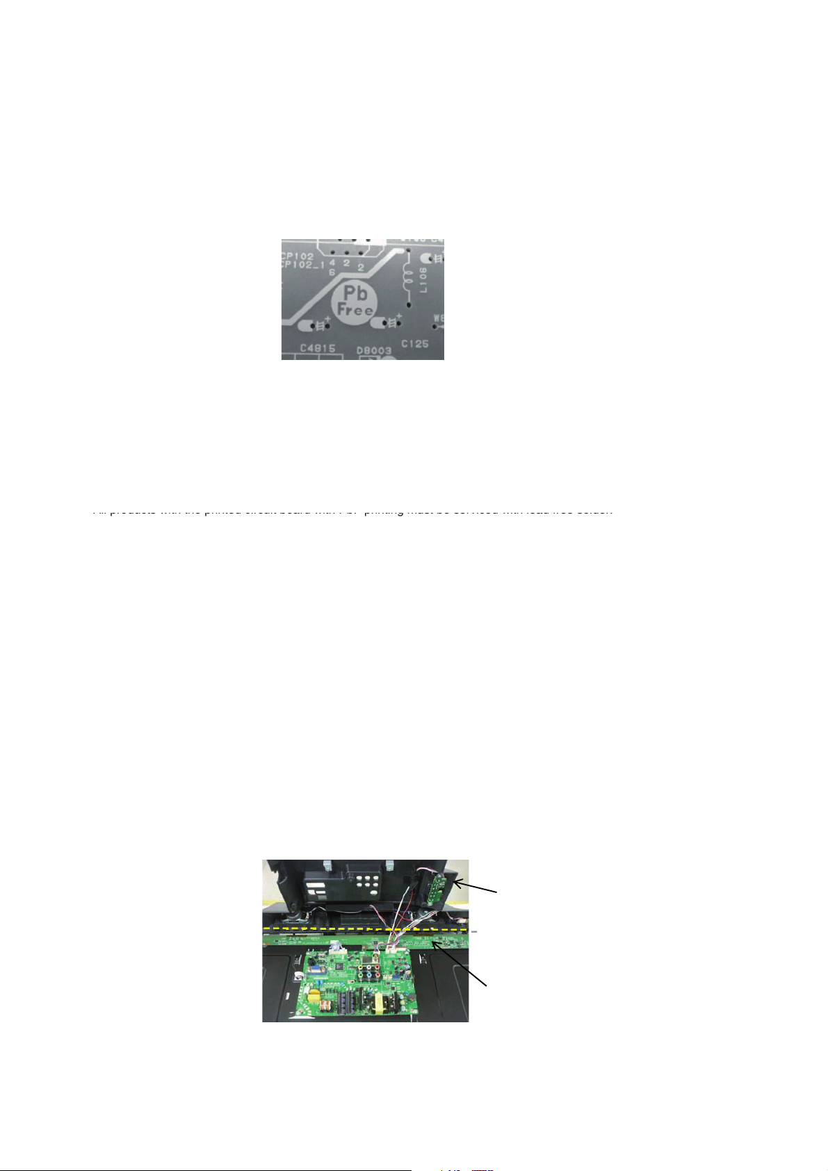
All products with the printed circuit board with PbF printing must be serviced with lead free solder.
ABOUT LEAD FREE SOLDER (PbF)
Distinction of PbF PCB:
PCBs (manufactured) using lead free solder will have a PbF printing on the PCB.
(Please refer to figures.)
Caution:
• Pb free solder has a higher melting point than standard solder;
Typically the melting point is 86
Please use a soldering iron with temperature control and adjust it to 650
In case of using high temperature soldering iron, please be careful not to heat too long.
•
Pb free solder will tend to splash when heated too high (about 1100
•
When soldering or unsoldering, completely remove all of the solder from the pins or solder area,
and be sure to heat the soldering points with the lead free solder until it melts sufficiently.
o
F~104oF(30oC~40oC) higher.
o
F ± 20oF (350oC ± 10oC).
o
F/ 600oC).
Recommendations
Recommended lead free solder composition is Sn-3.0Ag-0.5Cu.
CAUTION WHEN REMOVE THE REAR CABINET
1. Remove SCREWs from COVER BACK ASS'Y and hold the COVER BACK ASS'Y as the below Picture.
2. Remove connector of CD2201䇮CD2202䇮CD301 from MAIN PCB BOARD.
In doing so, take care the space NOT to touch T-CON PCB , COVER BACK ASS'Y must be held off the T-CON PCB
( as NOT over dashed line in below picture).
3. And then, also take care for cables NOT to be fallen down from RIBs on COVER BACK ASS'Y side.
COVER BACK
SPACE
T-CON PCB
A1-2
Page 4
/
pp
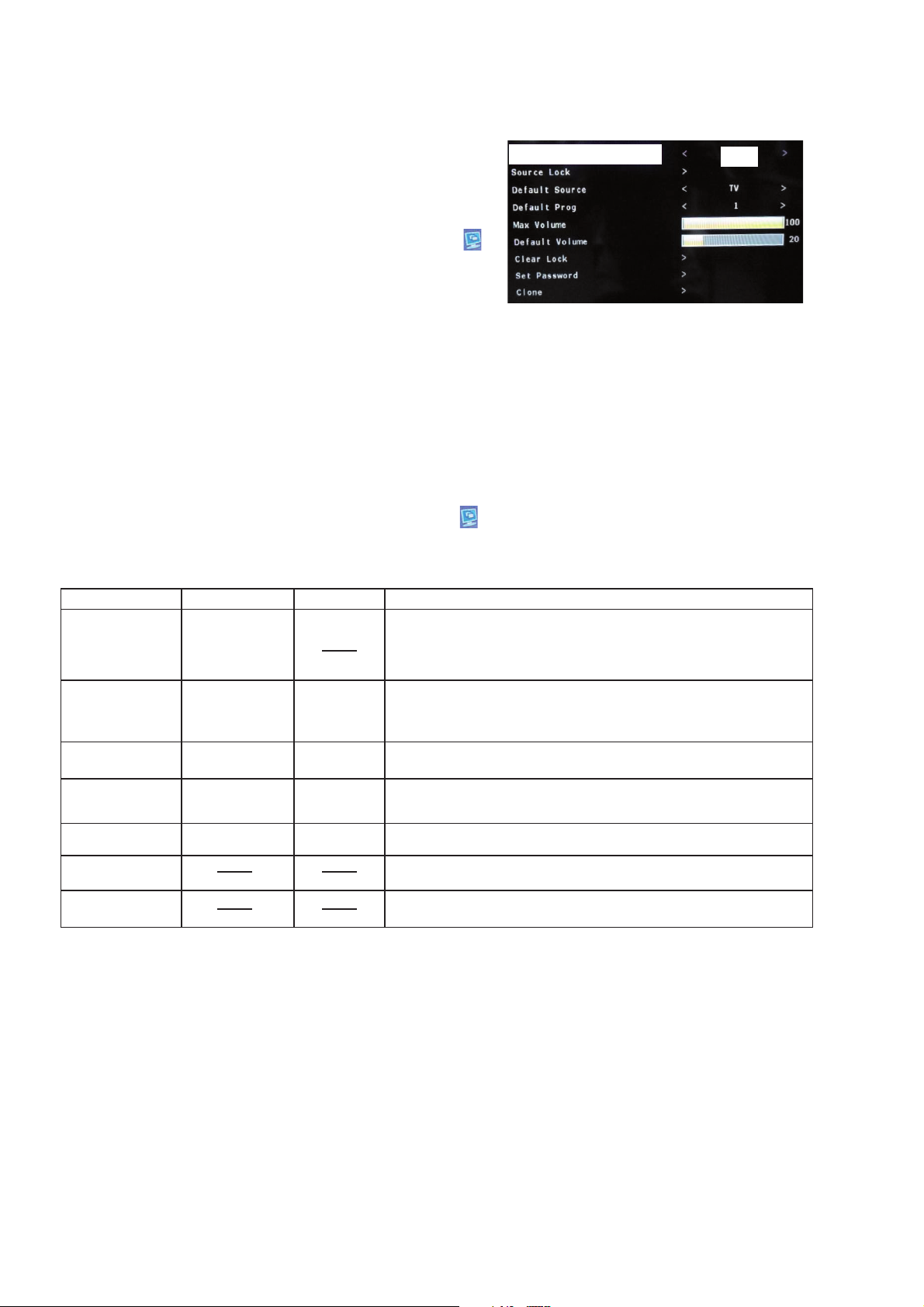
HOTEL MODE FUNCTION
To set the Hotel mode, please follow the steps below.
1. Press the MENU---> 1147 button on the remote control.
2. Press the DOWN button on the remote control,
3. Select the "GENERAL SETTING" menu , then press ENTER button.
Select the "Hotel Mode " menu, Select "ON",Then press the RETURN button.
4.
Using the LEFT/RIGHT button on the remote control, please select " ".
5.
Then press the ENTER button.
6.
Please input the password "0000". Then press the ENTER button.
7.
The Hotel mode setting menu will appear.
8.
9. Using the UP/DOWN button on the remote control,
select the desired mode. Then press the ENTER button.
10. Using the LEFT/RIGHT button on the remote control,
set the mode to desired setting.
11. The Hotel mode has now been set up.
To reset the Hotel mode, please follow the steps below.
1. Press the MENU---> 1147 button on the remote control.
2. Press the DOWN button on the remote control,
3. Select the "GENERAL SETTING" menu , then press ENTER button.
4. Select the "Hotel Mode " menu.
5. Using the LEFT/RIGHT button on the remote control, please select " ".
6. Then press the ENTER button.
7. Please input the password "0000". Then press the ENTER button.
8. The setting items has now been returned to initial value.
Hotel Mode
On
Setting item Setting value Initial value
TV/AV/
Source Lock COMPONENT/ Setting Input skip, combine with "Default Source".
HDMI/PC/MEDIA
Default Source
Default Prog
Maximum volume 0~100 100
Default Volume 0~100 20 Setting volume at Power on.
Clear Lock Setting of the Hotel Mode return factory setting.
Set Password Setting of the Password.
TV/AV
COMPONENT/ Setting Input Source, combine with "Source Lock"
HDMI/PC/MEDIA If select "Source Lock" for this function disa
0~199 1 Setting of the CH if select "Default Source" to TV input.
OFF
Setting of the maximum volume value.
FUNCTION
ear.
A1-3
A1-3
Page 5
GENERAL SPECIFICATIONS
G-1 TV
System
G-2 Tuning
System
G-3 Power
G-4 Regulation
G-5 Temperature
G-6 Operating Humidity
G-7 OSD Language
G-8 Clock and
Timer
G-9 Remote
Control
LCD LCD Size / Visual Size 22.95 inch / 583.0mmV
Color System PAL / SECAM / NTSC3.58 / NTSC4.43 / PAL60
Speaker 2 Speaker
Sound Output MAX 5W + 5W
Broadcasting System Analog
Tuner and System 1Tuner (Analog)
Receive CH Destination UK, I.R., CCIR Hyper
CH Coverage Analog 44.25MHz~863.25MHz
Intermediate Analog
Frequency Picture(FP) 38.9 / 38.9 / 38.9 / 45.75MHz
Auto Tuning Method
Preset CH Analog 199 Carrier
Stereo/Dual TV Sound Nicam / A2 Dual / US Stereo(w/ SAP)
Tuner Sound Muting Yes
Power Source AC 220-240V AC 50/60Hz
Power Consumption at AC 33 W at AC 220 V 50 Hz
Protector Power Fuse Yes
Sleep Timer Max Time 240 Min
On/Off Timer Program(On Timer / Off Timer) -- Program / -- Program
Timer Back-up (at Power Off Mode) more than -- Min Sec
EPG Timer Events -Unit RC-UW
Case Color Black
Glow in Dark Remocon No
Remocon Format SHARP
Format SHARP
Custom Code 10000 / 10001 / 01111
Power Source Voltage(D.C) 3V
Total Keys 43 Keys
Keys Power (Stand By) Yes
LCD Type Color TFT LCD
Number of Pixels 1366(H) x 768(V)
Double Scan No
View Range Left/Right 85/85 degree
Up/Down 85/85 degree
Bright Dot
Zero Bright Dot Ratio --
Position Bottom
Size 1.0 x 2.5 inch
Impedance 4 ohm
10%(Typical) ---
Sound(FS)
FP-FS
DC ---
at DC --
Stand by (at AC) w/ EPG Timer --
w/o EPG Timer 1 W at AC 230 V 50 Hz
Per Year -- kWh/Year
Safety
Radiation EN55013,EN55020,EN55022
X-Radiation Operation
Storage
Space Around Unit 100mm (4inch)
Step 10 / 20 / 30 / 60 / 90 / 120 / 180 / 240 Min
UM size x pcs UM-4 x 2 pcs
Information Yes
Analog Menu No
Digital Menu No
Input Select Yes
TV/DVB-T No
Guide No
Picture Size Yes
1 Yes
2 Yes
3 Yes
4 Yes
5 Yes
6 Yes
7 Yes
8 Yes
9 Yes
n҇0
PAL(B/G, D/K, I), SECAM(B/G, D/K)
BG / II / DK / M
33.4 / 32.9 / 32.4 / 41.25MHz
5.5 / 6.0 / 6.5 / 4.5MHz
ALL Band (Not C.C.I.R. CH Plan)
IEC60065 Ed.7:2001+Amd.1:2005, EAC(applied by
Sharp)
IEC61000-3-2, IEC61000-3-3
o
0
C ~ +40oC
o
-20
C ~ +60oC
Less than 80% RH
English, Simplified Chinese, Arabic, Thai, Persian
French, Vietnam, Russian, Malay, Portuguese,
Spanish, Indonesian
A2-1
A2-1
Page 6
GENERAL SPECIFICATIONS (continued)
0 Yes
Sleep No
Mute Yes
Volume Up / ń
Volume Down / ł
Volume Up Yes
Volume Down Yes
CH Down Yes
CH Up Yes
Menu Yes
㸡
㸣
㸠
㸢
MEDIA Yes
Enter / CH List Yes
Return / Index Yes
Freeze frame Yes
Quick View Yes
Audio 1/2 Yes
TV/Radio No
Subtitle No
Reveal Yes
HOLD Freeze Frame enable
Red Yes
Green Yes
Yellow Yes
Cyan Yes
F/T/B(Expand) Yes
Sub Page Quick View enable
Page Up CH Up enable
Page Down CH Down enable
STOP Yes
SEARCH > Yes
SEARCH < Yes
SKIP >> Yes
SKIP << Yes
Country No
TV Location No
Auto Power Off Yes
Auto tuning Yes
Auto clock (Digital tuner) No
Plug in start Yes
Brightness , Contrast , Color Yes
Tint Yes
Sharpness Yes
DNR Yes
Color Temperature Yes
Backlight Control Yes
DBC (Dynamic Backlight Control) No
Motion 100/120Hz No
Film Mode No
Brightness , Contrast , Color Yes
Sharpness No
HOR POSITION , VER POSITION Yes
PHASE , CLOCK Yes
AUTO ADJUST Yes
RED , GREEN , BLUE No
DNR No
Color Temperature Yes
Backlight Yes
WXGA INPUT No
WVGA INPUT No
G-10 Features
T'TEXT Keys TV / TEXT / MIX Yes
USB MEDIA Keys PLAY / PAUSE Yes
Power On Memory Yes
Auto Shut Off Yes
Just Clock Function No
Game Position No
DNR Yes
Comb Filter Yes
Auto Set Up (Fast installation) Language Yes
Picture Setting(TV) Picture Mode Yes
Picture Setting(PC) Picture Mode Yes
No
No
Yes
Yes
Yes
Yes
3D
3D
CH sort No
ATS No
A2-2
Page 7
GENERAL SPECIFICATIONS (continued)
Audio Sound Mode Yes
Tuning Auto Tuning Yes
Lock Key Lock Yes
Screen Saver
T'Text Yes
Text and Picture No
Wide Mode (4:3/16:9/CINEMA/REAL) Yes
CH Label Yes
Reset to Default Yes
HD Zoom No
Picture Scroll (Vertical Position) No
PFC(Power Factor circuit) No
Freeze frame Yes (ATV/CVBS in Only)
Plug and Play No
Power Management Yes
Hearing Impaired No
Audio Description No
Power On LED No
HDMI Mode No
Blue Back Yes
Scart Spec Scart1 AV in No
Scart2 AV in No
Digital Text (VBI teletext)
MHEG-5
MHP
EPG (BBC type 8Days Digital tuner only)
OAD (Over Air Download)
Common Interface (Digital tuner only)
Rec Screen Status
Ch sorting based on Ch List (Digital/Germany only)
Rename Carrier (Digital)
Edit Event Timer
Software Update via CI Slot
Preference Language (Audio/Subtitle/Digital Service)(Digital)
DVB Subtitle (Digital)
Clock
DST
Signal Status
Digital Out Dolby Digital No
Decode(Down Mix) Dolby Digital No
Tone Control (Bass/Treble/Balance) Yes
Surround Yes
Equalizer No
Speaker No
Auto Volume Yes
BBE No
SRS WOW (SRS 3D/Focus/Tru Bass) No
Variable Audio Out No
Manual Tuning Yes
Update Scan No
CH Skip Yes
CH Move Yes
CH Del Yes
Fine Tuning Yes
Channel Lock No
Parental Lock (Digital) No
Hotel Lock Yes
USB Clone (Hotel Lock) Yes
Inversion No
Full White No
Screen Saver No
Static Image No
Text type Fastext / Toptext
Text Language English, German, Swedish, Finnish, Hungarian,
AV out No
S-Video in No
RGB in No
AV out No
S-Video in No
RGB in No
Dolby Digital Plus No
MPEG No
HE AAC No
Dolby Digital Plus No
Italian, French, Portuguese, Spanish, Czech,
Slovak, Polish, Estonian, Lettish, Lithuanian,
Slovenian, Rumanian, Russian,
Ukrainian, Turkish, Greek, Hebrew, Farisi
Arabic, Serbian, Croatian, Bulgarian
No
No
No
No
No
No
No
No
No
No
No
No
No
No
No
No
A2-3
Page 8
GENERAL SPECIFICATIONS (continued)
MPEG No
HE AAC No
USB Media Player Photo JPEG (.jpg/.jpeg), BMP (.bmp), PNG (.png)
Music MP3 (.mp3), WMA (.wma), AAC (.aac/.m4a)
Video Container AVI (.avi), MKV (.mkv), MP4 (.mp4),
Video Codec Xvid, MPEG1, MPEG2, MPEG4 SP/ASP,
Audio Codec MPEG2, MP3, PCM/ADPCM, WMA, AC-3, AAC
Text Text (.txt)
PC Monitor Input Yes
VGA (640x480) Yes (60Hz)
VGA (720x400) No (Possible to Display)
WVGA (848x480) No
SVGA (800x600) Yes (60Hz)
XGA (1024x768) Yes (60Hz)
WXGA (1280x768) Yes (60Hz)
WXGA (1280x720) Yes (60Hz)
WXGA (1360x768) Yes (60Hz)
SXGA (1280x1024) Yes (60Hz)
WXGA+ (1440x900) Yes (60Hz)
WSXGA+ (1680x1050) No (Possible to Display)
FULL HD (1920x1080) Yes (60Hz)
HDMI Input Yes
VGA (640×480)
VGA (720x400) No (Possible to Display)
WVGA (848x480) No
SVGA (800x600) Yes (60Hz)
XGA (1024x768) Yes (60Hz)
WXGA (1280x768) Yes (60Hz)
WXGA (1280x720) Yes (60Hz)
WXGA (1360x768) Yes (60Hz)
SXGA (1280x1024) Yes (60Hz)
WXGA+ (1440x900) Yes (60Hz)
WSXGA+ (1680x1050) No (Possible to Display)
FULL HD (1920x1080) Yes (60Hz)
720×480i (4:3)
720×480i (16:9)
720×480p (4:3)
720×480p (16:9)
720×576i (4:3)
720×576i (16:9)
720×576p (4:3)
720×576p (16:9)
1280×720p
1920×1080i
1920×1080p
CEC(ORION Standard)
Deep Color
xvYCC
Component Input Yes
720×480i (4:3)
720×480i (16:9)
720×480p (4:3)
720×480p (16:9)
720×576i (4:3)
720×576i (16:9)
720×576p (4:3)
720×576p (16:9)
1280×720p
1920×1080i
1920×1080p
Wall Mount Size W x H(mm) Yes (100 x 100)
Screw Size M4 x 10
Stand Tilt No
Swievel No
PS (.mpg), TS (.ts/.trp), VOB (.vob)
DIVX(.div/.divx/.avi/.mp4), MOV(.mov)
MJPEG, H.264, DIVX
Yes (60Hz)
Yes (60Hz)
Yes (60Hz)
Yes (60Hz)
Yes (60Hz)
Yes (50Hz)
Yes (50Hz)
Yes (50Hz)
Yes (50Hz)
Yes (50/60Hz)
Yes (50/60Hz)
Yes (24/50/60Hz)
No
No
No
Yes (60Hz)
Yes (60Hz)
Yes (60Hz)
Yes (60Hz)
Yes (50Hz)
Yes (50Hz)
Yes (50Hz)
Yes (50Hz)
Yes (50/60Hz)
Yes (50/60Hz)
No (Possible to Display)
A2-4
Page 9
GENERAL SPECIFICATIONS (continued)
G-11 Accessories
G-12 Interface
G-13 Set Size
G-14 Weight
Owner's Manual Language Russian/Kazak (w/EAC number)
Remote Control Unit Yes
DVB-T Antenna No
U/V Mixer No
Information Sheet (VESA) No
DC Car Cord (Center+) No
Warranty card Yes(w/Serial No, Model No. label)
EAC Safety sheet Yes ( for AUG'14 O/R only)
Warning Sheet No
Circuit Diagram No
Antenna Change Plug No
Service Facility List No
Important Safeguard No
Quick Set-up Sheet No
Battery Yes
AC Adapter No
AC Cord (for AC Adapter) No
AC Cord No
AV Cord (2Pin-1Pin) No
HDMI-DVI Cable No
Registration Card No
300 ohm to 75 ohm Antenna Adapter No
Stand Screw??? Yes (4pcs)
Stand Yes
Frame Stand No
Switch Side Power (Tact) Yes
Indicator Power/Stand-by Yes(Green / Red)
Terminals Rear Video Input 1
w/Guarantee Card No
UM size x pcs UM-4 x 2 pcs
OEM Brand No
System Select No
Main Power SW No
Channel Up/Menu Up Yes
Channel Down/Menu Down Yes
Volume Up/Menu > Yes
Volume Down/Menu < Yes
Input Select/Enter Yes
Menu No ("Vol-"+"Vol+" 1sec)
On Timer No
Audio Input 1
S- Input 1 No
Video Input 2 No
Audio Input 2 No
S- Input 2 No
Video Output No
Audio Output No
Digital Audio Out (Coaxial) No
Euro Scart (21Pin) No
Component In
Audio Input (Component In use)
HDMI Input 1
Audio Input (HDMI/DVI In use) PC Monitor Audio Input enable
HDMI Input 2 No
Audio Input (HDMI/DVI In use) No
PC Monitor Input (D-Sub)
Audio Input
USB
Sub Woofer Output No
Diversity No
Ext Speaker No
DC Jack 12V(Center +) No
VHF/UHF Antenna Input
Headphone No
CI Card Slot No
AC Inlet No
Approx. W x D x H (mm) 542 x 136.9 x 350.5
w/o Stand,Handle Approx. W x D x H (mm)
Net Approx. 3.0 kg (6.6lbs)
Net w/o Stand,Handle Approx. 2.8 kg (6.2lbs)
Gross Approx. 4.1 kg (9.1lbs)
Gross w/Master Carton (Approx.) --- kg ( --- lbs)
RCA x 1
RCA x 2(L, R)
RCA x 3
Audio Input1 enable
Yes
Yes
Mini Pin Jack(Ǘ3.5), STEREO
Yes
DIN Type
542 x 57.5 x 326.5
A2-5
Page 10
GENERAL SPECIFICATIONS (continued)
G-15 Carton
G-16 Material
G-17 Environment
Master Carton No
Gift Box Yes
Drop Test Natural Dropping At 1 Corner / 3 Edges / 5 Surfaces
Container Stuffing 2400 Sets/40' hi-cub container
w/Pallet No
w/Wrapping No
Cabinet Cabinet Front PS 94HB (Piano)
PCB Non-Halogen No
Environmental standard requirement Green procurement of SHARP
Pb- Free Phase3(PHASE3A)
WEEE No
Content ---- Sets
Material -- /-Dimensions W x D x H(mm) -- x -- x --
Description of Origin No
Material Single/Full Color
W/Color Photo Label No
W/Handle
Dimensions W x D x H(mm) 589 x 113 x 390
Design As per Buyer's
Description of Origin Yes
Height (cm) 48 (ES:+15%, PP:+5%)
Cabinet Rear PS 94V0 NON-DECABROM
Speaker Box -Stand PS 94HB (Piano)
Eyelet Yes
Measures for Whisker Yes
Yes
A2-6
Page 11
(A)
g
g
(
)
(
)
y
(
)
y
(1)
g
(
(2)
(B)
pp
p
(D)
y
Fig.1
3
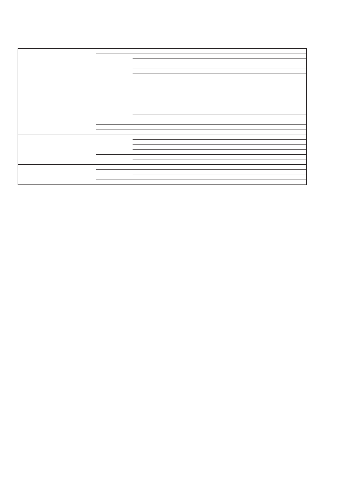
DISASSEMBLY INSTRUCTIONS
1. REMOVAL OF MECHANICAL PARTS
1-3: MAIN UNIT (Refer to Fig. 1-3)
AND P.C. BOARDS
1. Remove the 5 screws (1).
2. Remove the Shield Main in the direction of arrow
CAUTION
Parts removal shuld be perform in clean room cause 4. Remove the Main Unit in the direction of arrow (B).
•
the unit will be dero
Be careful not to remove the LVDS cable forcibly, because
•
the LVDS cable may be damaged.
To wear the gloves each time.
•
1-1: STAND ASS'Y
Remove the 4 screws (1).
1.
Remove the Stand Ass'y in the direction of arrow.
2.
1-2: COVER BACK ASS'Y
1. Remove the 11 screws
2. Disconnect the followin
ate by dust.
Refer to Fig. 1-1
Stand Ass'y
Refer to Fig. 1-2
.
connectors:
(1)
(1)
(1)
Fig. 1-1
(1)
CD301, CD2201 and CD2202).
3. Remove the Cover Back Ass'y in the direction of arrow (A).
4. Remove the 2 screws
5. Remove the Sheet PC in the direction of arrow
6. Unlock the su
7. Remove the O
eration PCB in the direction of arrow (C).
.
.
ort (3).
8. Unlock the 2 supports (4).
9. Remove the Remocon PCB in the direction of arrow
(1)
(1)
(1)
(1)
Cover Back Ass'y
(A)
Operation PCB
(1)
(1)
(1)
(1)
(3)
(1)
(1)
(C)
(D)
(B)
Remocon PCB
.
(1)
(4)
3.
Disconnect the followin
Shield Main
Main Unit
1-4: LED MODULE ASS'Y
connectors: (CN12 and CNB802).
(1)
(1)
(1)
(A)
(1) (1)
(B)
Refer to Fig. 1-4
1. Unlock the 14 supports (1).
2. Remove the LED Module Ass'
in the direction of
arrow (A) -> (B) -> (C) -> (D), Please remove carefully
(1)
(1)
.
(A)
(B)
(D)
(1)
(1)
Front Cabi Ass'y
LED Module Ass'y
.
and slowl
• Do not touch LED Module Ass'
.
-
(C)
(1)
(1)
Fig. 1-4
(2)
(2)
Sheet PC
Fig. 1-2
B1-1
Page 12
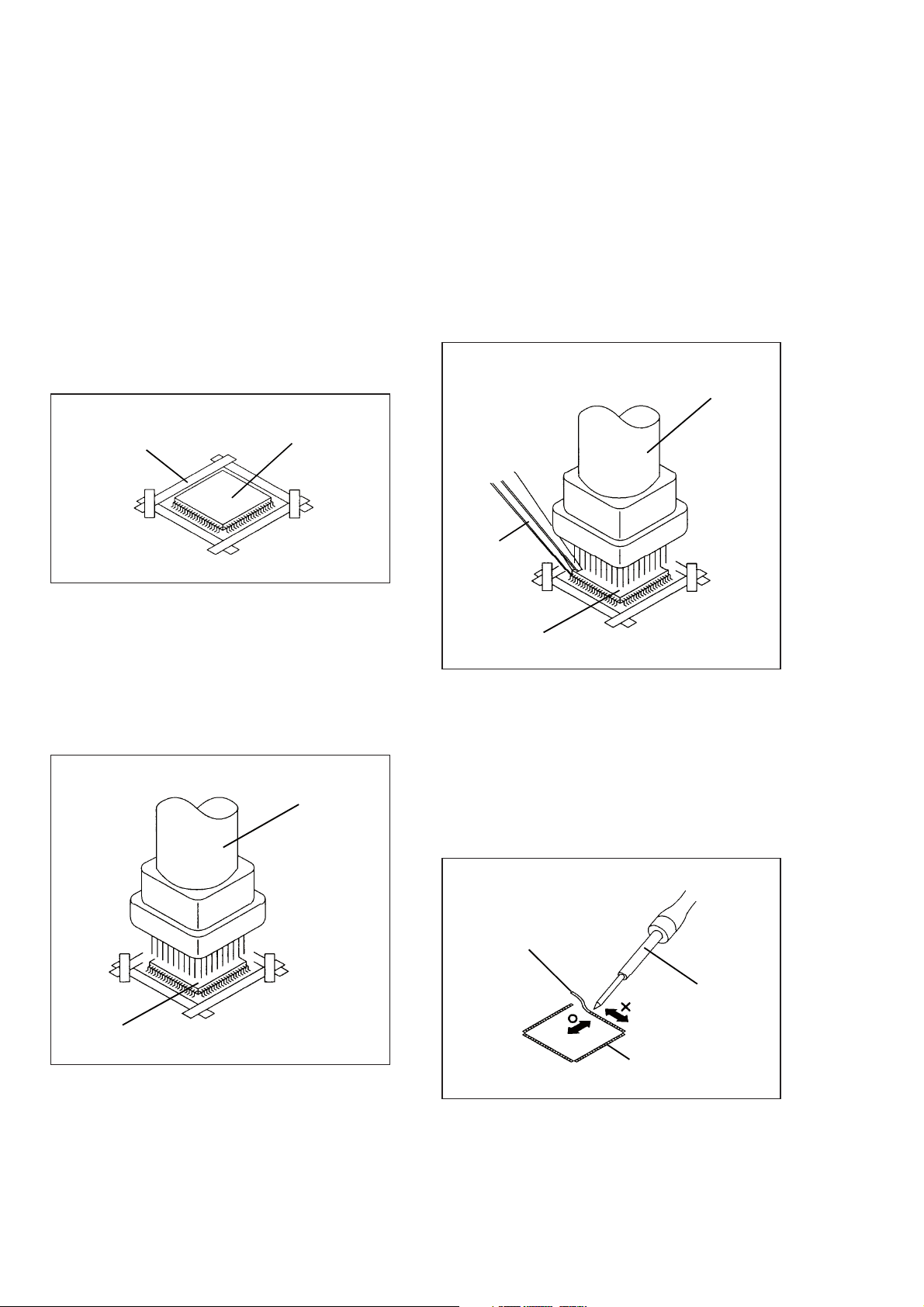
Fig.2-1
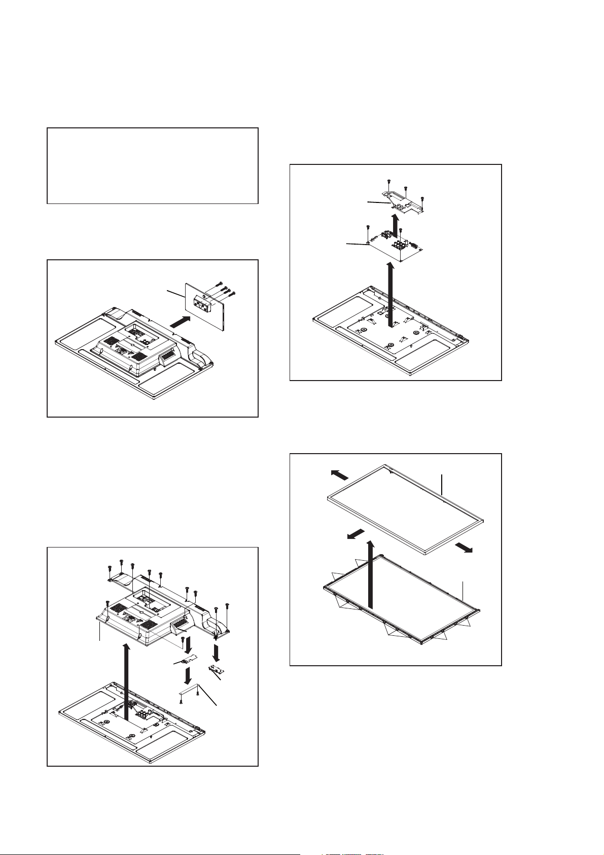
DISASSEMBLY INSTRUCTIONS (continued)
2. REMOVAL AND INSTALLATION OF
FLAT PACKAGE IC
3. When IC starts moving back and forth easily after
desoldering completely, pickup the corner of the IC using
tweezers and remove the IC by moving with the IC
REMOVAL desoldering machine. (Refer to Fig. 2-3.)
1. Put Masking Tape (cotton tape) around the Flat Package
NOTE
IC to protect other parts from any damage.
(Refer to Fig. 2-1.)
Some ICs on the PCB are affixed with glue, so be
careful not to break or damage the foil of each IC
NOTE
leads or solder lands under the IC when removing it.
Masking is carried out on all the parts located within
10 mm distance from IC leads.
Masking Tape
(Cotton Tape)
IC
Tweezers
Blower type IC
desoldering machine
2. Heat the IC leads using a blower type IC desoldering
machine. (Refer to Fig. 2-2.)
IC
NOTE
Fig. 2-3
Do not rotate or move the IC back and forth , until IC 4. Peel off the Masking Tape.
can move back and forth easily after desoldering the
leads completely. 5. Absorb the solder left on the pattern using the Braided
Shield Wire. (Refer to Fig. 2-4.)
Blower type IC
desoldering machine
NOTE
Do not move the Braided Shield Wire in the vertical
direction towards the IC pattern.
Braided Shield Wire
Soldering Iron
IC
Fig. 2-2
IC pattern
Fig. 2-4
B2-1
Page 13

damaged. So, always be sure to replace the IC
s
damaged. So, always be sure to replace the IC in this
DISASSEMBLY INSTRUCTIONS (continued)
INSTALLATION
4. When bridge-soldering between terminals and/or the
soldering amount are not enough, resolder using a
1. Take care of the polarity of new IC and then install the
Thintip Soldering Iron. (Refer to Fig. 2-8.)
new IC fitting on the printed circuit pattern. Then solder
each lead on the diagonal positions of IC temporarily.
(Refer to Fig. 2-5.)
Thin-tip Soldering Iron
Soldering Iron
IC
Fig. 2-8
5. Finally, confirm the soldering status on four sides of the
IC using a magnifying glass.
Confirm that no abnormality is found on the soldering
Solder temporarily
Solder temporarily
Fig. 2-5
position and installation position of the parts around the
IC. If some abnormality is found, correct by resoldering.
NOTE
2. Supply the solder from the upper position of IC leads When the IC leads are bent during soldering and/or
sliding to the lower position of the IC leads. repairing, do not repair the bending of leads. If the
(Refer to Fig. 2-6.)
bending of leads are repaired, the pattern may be
in thi
case.
Solder
Soldering Iron
Supply soldering
IC
from upper position
to lower position
Fig. 2-6
3. Absorb the solder left on the lead using the Braided
Shield Wire. (Refer to Fig. 2-7.)
NOTE
Do not absorb the solder to excess.
Soldering Iron
IC
Braided Shield Wire
Fig. 2-7
B2-2
Page 14

p
HOW TO UPGRADE SOFTWARE
Turn off and Unplug the AC cord.
1
Connect the USB storage device into the Media input terminal while turning off.
2
Insert the AC cord plug and press hold Power untill the flashing.
3
If the LED light is flashing, Power Key is leaved, Then wait 50 sec. after that let update data.
4
(Do not be closed the light while updating. If it closes, please update data again.)
Power on at Power key then the OSD will appear on the screen It is finished updating data.
5
Unplug and remove the USB.
6
Unplug the Ac cord and disconnect the USB, then insert plug.
7
Power on and check version to follow that "MENU ---> 1147 ---> FACTORY SETTING --->VERSION".
8
To process the "FACTORY SETTING" "INIT TV" and to set the first time installation bofore dirivery.
9
CHECK FOR THE FIRMWARE VERSION
This unit is
CAUTION
1.
rovided with the following SERVICE MODES so you can repair, examine and adjust easily.
Do not adjust other items except " SW INFORMATION".
Check of the SUM DATA and VERSION on the screen.
1-1: Press the MENU ---> 1147 button on the remote control.
1-2:
The "Factory Setting" menu on the screen as shown in Fig. 1-1.
Factory Setting
GENERAL SETTING
PICTURE
SOUND
DEBUG
ADC ADJUST
EMC SETTING
SW INFORMATION
Software Update (USB)
INIT FAC CHANNEL >>>
INIT TV >>>
BURN MODE OFF
BUILD TIME 2014-07-18 11:53:45
VERSION M3SS-05X
LSC230AN01
23_SH_M3SS_05X_V59_DivX
BD_VST59_P901A
Checksum 9CB6
Fig. 1-1
1-3: Press the DOWN button on the remote control, Select the "SW INFORMATION" menu,
then press ENTER button.
1-4:
The SW INFORMATION menu on the screen as shown in Fig. 1-2.
SW INFORMATION
BUILD TIME
VHF_L_H 163
VHF_H_UHV 467
WDT ON
MANTIS NO.
AT:V2.72
LCD ON TIME 6
HDCP INFO: 0x000EF905
AT Tested Status CHECKED
LSC230AN01
23_SH_M3SS_05X_V59_DivX
BD_VST59_P901A
Checksum
CS55400
9CB6
Fig. 1-2
1-5: After the confirmation of each check sum. Turn off power.
C-1
Page 15

.
ELECTRICAL ADJUSTMENTS
1. ADJUSTMENT PROCEDURE
Prepare the following measurement tools for electrical
adjustments.
1. Pattern Generator 2. Please select input About mode to adjust COLOR TEMP
On-Screen Display Adjustment
1. Press the MENU---> 1147 button on the remote control. to set to the AV mode.
2. Press the DOWN button on the remote control. 5. Using the remote control, set the brightness and
3. Select the "PICTURE SETTING" menu, then press contrast to normal position.
ENTER button on the remote control. 6. Press the MENU---> 1147 button on the remote control.
4. Select the "COLOR TEMP" menu , then press 7. Press the DOWN button on the remote control.
ENTER button on the remote control. 8. Select the "PICTURE SETTING" menu, then press
5.
On the screen as shown in Fig. 1-1.
SOURCE < HDMI >
COLOR TEMP < COOL >
R GAIN 149
G GAIN 128
B GAIN 149
R OFFSET
G OFFSET
B OFFSET
COPR ALL
RESET
1005
1010
990
2. BASIC ADJUSTMENTS
2-1: WHITE BALANCE
1. Place the set in Aging Test for more than 15 minutes.
3. Receive the gray scale pattern from the Pattern
Generator.
4. Press the INPUT SELECT button on the remote control
ENTER button on the remote control.
9. Select the "COLOR TEMP" menu , then press
ENTER button on the remote control.
10. Press the UP/DOWN button on the remote control
to select the "R GAIN", "B GAIN", "R OFFSET",
"B OFFSET".
11. Adjust the LEFT/RIGHT button on the remote control
to whiten the R GAIN, B GAIN, R OFFSET, B OFFSET
at each step tone sections equally.
12. Perform the above adjustments 8 and 9 until the white
color is achieved.
BD_VST59_P901A
-
D-1
Page 16

ELECTRICAL ADJUSTMENTS (continued)
3. ELECTRICAL ADJUSTMENT PARTS LOCATION GUIDE (WIRING CONNECTION)
LCD PANEL
CN5
MAIN UNIT
CN6
CN18
SP301
SPEAKER
CD2202
CP2202
OPERATION PCB
CN12
CNB1
CNB802
CD503
AC IN
CD2201
OS2201
CP2201
REMOCON PCB
D-2
Page 17

(LCD SECTION)
Y
Power does not turn on
AC cord is connected
to the CNB1?
Check FB1 Broken.
TROUBLESHOOTING GUIDE
No
Connect AC Cord to CNB1
㪰㪼㫊
No
Change FB1
es
Does 2 pins of DB101 have
the voltage of 12V?
Yes
Does 2 pins of DB102
have the voltage of 6.5V?
Yes
No
Change DB101
No
Change DB102
Change Main board.
E-1
Page 18

N
TROUBLESHOOTING GUIDE (continued)
The Picture appears,
but the audio does not appears
No
Is Speaker connected?
Yes
Is there signal at pins 1
and 4 of CN18?
o
Change Main board
Connect Speaker
Yes
Change Speaker
E-2
Page 19

TROUBLESHOOTING GUIDE (continued)
Panel does not light.
No
CP2000 is connected
to the CNB802?
㪰㪼㫊
Connect CP2000 to CNB802
Does 1䌾3 pins of CNB802
have the voltage of 11V?
No
Does 1 pins of UB801 have
the voltage of 12V?
No
Change Main board
Yes
Change Panel
Yes
Change UB801
E-3
Page 20

TROUBLESHOOTING GUIDE (continued)
The picure does not appear
No
CD2801 is connected
to the CN12?
Yes
Connect CD2801 to CN12
CD2801 is
connected
to the Panel?
No
CN12 have signal and
voltage of 12V?
No
Change Main board
Yes
Connect CD2801 to Panel
Yes
Change panel
E-4
Page 21

TROUBLESHOOTING GUIDE (continued)
The color does not appear
No
Is Setting of color Normal?
Yes
Is the color signal received?
No
Is there color signal at IC U9?
No
Adjust the color setting
Yes
Receive the color signal.
Yes
Check U9(TSUMV59XE) and
peripheral circuit.
Change Main board
E-5
Page 22

BLOCK DIAGRAM
Audio
Component
In Jack
HDMI
Connector
HDMI
Audio Mini Jack
PC In
PC & DVI Audio
Analog RGB
Component
Video In
(D-Sub 15 pin)
Pr
PC Input
Pb
Y
HSYNC/VSYNC
CVBS In
R
V
䌌
UBS
Silicon Tuner
R620D2
Speaker
SOUND AMP
TPA3110LD2PWP
R
Key A
Key B
Key A/Key B
<Operation PCB>
SCALER+LVDS+AUDIO DECORDER
Mstar
TSUMV39LE or TSUMV59XE
<MAIN >
Remocon In
Serial FLASH 32Mbit
GD25Q16BSIG
(GIGA)
ฃశㇱ
Remocon
Remocon
<Remocon PCB>
Speaker OUT
<LCD Panel>
F-1
Page 23

PCB
102
PCB
101
+
EB
106
GND
PCB
102
PCB
101
+
EB
106
GND
BLOCK DIAGRAM (continued)
Power
TB101
DB102
6
䋱
6.5V
+ +EB102 EB103
7
DB101
11
3
QB101
12V
10
EB101
+
5
9
4
DB104
8
SGND
DB2
LCB1
FB1CNB1
6
5
5
VCC
OTP
3
COMP
2
+ +EB1 EB2
SGND
DB1
DB3
UB101
OUT
OUT
CS
4
GND
1
DB4
3
2
䋱
4
AC_IN
F-2
Page 24

PRINTED CIRCUIT BOARDS
OPERATION (INSERTED PARTS)
SOLDER SIDE
SW2204
SW2202
CEM844A
SW2205
SW2206
SW2201
SW2203
CP2202
OPERATION (CHIP MOUNTED PARTS)
SOLDER SIDE
C2202
C2201
R2202
R2201
R2204
CEM844A
R2203
REMOCON (INSERTED PARTS)
SOLDER SIDE
CEM846A
D2201
CP2201
OS2201
REMOCON (CHIP MOUNTED PARTS)
SOLDER SIDE
R2210
R2209
CEM846A
R2208
C2203
C2204
G-1
Page 25

SCHEMATIC DIAGRAMS
2
C2208 *
123
GND
3
PCB270
CEM844
KEYB
KEYA
CD2202
06EH232202
KEY‑A
KEY‑B
4
CP2202
FROM/TOMICON
A2001WR‑3A
B
PCBDA0
5
CEM846
FROM/TOMICON
CP2201
7
A2001WR‑5A
12345
GND
REMOCONIN
AT+5VAT+3.3V
STANDBYLED
POWERONLED
8
CD2201
6
CH252005
GND4
1
WASRECEIVEDINGOODCONDITIONANDPICTUREISNORMAL.
WITHTHEDIGITALTESTERWHENTHECOLORBROADCAST
NOTE:THEDCVOLTAGEATEACHPARTWASMEASURED
D2201
STANDBY/POWER
330 1/16W
LTL‑1BEFJ‑002A
G
R2210
(REMOCONPCB)
330 1/16W
R2209
R
3
(OPERATION/REMOCONPCB)
R2208
47 1/16W
OPERATION/REMOCONSCHEMATICDIAGRAM
123
B+
GND
OS2201
Vout
S‑R531F‑H451‑B
6.3V
22
B
C2203
226.3V B
C2204
12
(OPERATIONPCB)
CH‑
SW2206
SW2205
VOL+
SW2204
POWER
SW2203
VOL‑
CH+
EVQ21505R
EVQ21505R
EVQ21505R
EVQ21505R
EVQ21505R
SW2202
EVQ21505R
SW2201
INPUT/ENTER
R2204
11K 1/16W
R2203
1.8K 1/16W
R2202
2.7K 1/16W
OFPRINTINGANDSUBJECTTOCHANGEWITHOUTNOTICE
NOTE: THISSCHEMATICDIAGRAMISTHELATESTATTHETIME
R2201
6.8K 1/16W
ABC D E F GH
8
ABC D E F GH
7
6
5
4
3
2
1
H-1
Page 26

SCHEMATIC DIAGRAMS (continued)
8
7
6
5
4
3
2
1
ARE
VFM1
LCDPANEL
DESCRIBEDINPARTSLISTONLY
CRITICALFORSAFETY,USEONES
CD2801
1
45678
9
GND
GND
GND
ORX1‑
ORX0+
ORX0‑
101112131415161718
ORX2+
ORX2‑
ORX1+
CP12
VCC
VCC
CEC
HOTPLUG
DDCGND
DDCSDA
DDCSCL
+5VPOWER
RESERVED
TMDSCLK‑
TMDSCLK+
TMDSDATA1‑
TMDSDATA2‑
TMDSDATA1+
TMDSDATA0+
TMDSDATA0‑
TMDSCLKSH
TMDSDATA0SH
TMDSDATA1SH
TMDSDATA2SH
9
19
CN14
5
6
E
HH
3
4
AV1
E
YPbPr
1
2
H
E
101112131415161718
2345678
TMDSDATA2+
1
VCC
GND
GND
ORX3+
ORX3‑
OCLK+
OCLK‑
192202122232425262728
GND
GND
ERX2+
ERX2‑
ERX1+
ERX1‑
ERX0+
ERX0‑
29330
MAINPCB
ERX3+
ERX3‑
ECLK+
ECLK‑
TP.VST59.PA901
:SINCETHESEPARTSMARKEDBY
CAUTION
5
6
E
HH
3
4
AV4
E
AVIN
1
2
H
E
123
4
VS
SCL
GND
+5V
USBP
USBN
INTERCONNECTIONDIAGRAM
CN10
15
CN9
1
3
21
CD503 CNB1
HS
CNB802
CP2000
9
1011121314
LED+
LED+
LED+
12345
12345
VLED
VLED
VLED
LED‑FB
GNDNCGNDNCSDA
GND
LED‑FB
LED‑FB
6
6
PCBXX0
LEDBARPCB
12V
12V
GND
GND
NC
LED+
LED‑FB
PWM‑DIM
CNB801
1
2
CN5
CD2201
CP2201
OS2201
123
CNT1
GND
IR
AT+3.3V
54312
1REMOCONIN
GND
AT+3.3V 3
12345
VoutB+GND
123
TM101
AT+3.3V
LEDG
LEDR
12345
542
STANDBYLED
POWERONLED
COMMANDTRANSMITTER
123
4
CNB2
123
CN6
GND
KEYB
KEYA
321
CD2202
321
GND
KEYA
CEM846
PCBDA0
REMOCONPCB
G
1 2
R
D2201
3
STANDBY/POWER
KEYB
PCB270
CEM844
OPERATIONPCB
123
CP2202
123
4
CN18
SPOUTL+
SPOUTL‑
SPOUTR‑
SPOUTR+
4
3
2
1
SP301
SPEAKER
SPEAKER
NC
GND
GND
VGAR
VGAG
VGAB
1
2345678
T5
1
N1N1N1
CEN948
ABC D E F GH
8
ABC D E F GH
7
6
5
4
3
2
1
H-2
Page 27

SCHEMATIC DIAGRAMS (continued)
Main Unit
8
7
6
5
4
3V3 TEST
+5V M_5V
+3.3V_STB
5V-M
+3.3V_STB
U1
+5V
TEST
2
VO
VI
3
Q4
C13
CL1
4
VO
ADJ
1
C40.1uF-0402-Y5V-+80%-20%-16V
CL2
LC1117CLTR33
10uF-0603-X5R-20%-6. 3V
NC/10uF-0805-Y5V-+80%-20%-10V
C5
CM4
R12
R9
R89
0.1uF-0402-Y5V-+80%-20%-16V
100Kohm-0402-1%-1/ 16W
4K7ohm-0402-5%-1/ 16W
0.1uF-0402-X5R-20%-16V
Q5
R14
10Kohm-0402-5%-1/ 16W
PWR-ON/OFF
4K7ohm-0402-5%-1/ 16W
0.1uF-0402-Y5V-+80%-20%-16V
WPM2341A-3/TR
LMBT3904LT1G
TEST
2V5/1V8
UL41
M_5V DDR-2.5V/1.8V
VCC_P
TEST
C40
Q8
C39
0.1uF-0402-Y5V-+80%-20%-16V
200Kohm-0402-1%-1/ 16W
AO3407A
DM1
R38
R36
PVCC+5V
PVCC12V
R12V
R5V
CL43
CL44
2
4
VO
VO
ADJ
VI
3
CL42
CL41
PVCC VCC-Panel
Q10
+
ED10
0ohm-0805-5%-1/ 8W
NC/0ohm-0805-5%-1/ 8W
GND
1
GNDGND
0.1uF-0402-Y5V-+80%-20%-16V
10uF-0603-X5R-20%-6. 3V
0.1uF-0402-Y5V-+80%-20%-16V
NC/10uF-0805-Y5V-+80%-20%-10V
LC1117CLTR18
4K7ohm-0402-5%-1/ 16W
0.22uF-0402-X5R-10%-16V
R101
R39
PWR-ON/OFF
PMLL4148L-F
ć-XF
4K7ohm-0402-5%-1/ 16W
100uF-16V-20%-6 7-105
ADJ/Vs-ON
LMBT3904LT1G
2K2ohm-0402-5%-1/ 16W
TEST
R4
BL-ADJ PWM-DIM
510ohm-0402-5%-1/ 16W
8
7
6
5
4
+5V
CD121
TEST
TEST
LD12
3
BS
NC
2
12V
CD15
CD14
+5V
SW
IN
+
ED11
RD12
CD1
RC13
UD11
5
FB
COMP
6
GND
4
EN
7
RD11
+
ED1
ć-XF
3K3ohm-0402-1%-1/ 16W
100uF-16V-20%-6 7-105
18Kohm-0402-1%-1/ 16W
NC/22pF-0402-NPO-5%-50V
CD16
RD14
CD17
ć-XF
220pF-0402-X7R-10%-50V
RT7257GHZSP
3300pF-0402-X7R-10%-50V
0.1uF-0402-Y5V-+80%-20%-16V
100Kohm-0402-1%-1/ 16W
470uF-16V-20%-8 12-105
1uF-0603-X5R-10%-25V
B B
10uF-0805-Y5V-+80%-20%-10V
0.1uF-0402-Y5V-+80%-20%-16V
10uF-0805-Y5V-+80%-20%-10V
22Kohm-0402-1%-1/ 16W
RD6
CD3
CD42
3
SCD54TL-4R7M
10ohm-0402-5%-1/ 16W
0.1uF-0402-Y5V-+80%-20%-16V
2
12V 12V
PWM-DIM PWM-DIM
1
+3.3V_STB +3.3V_STB
A A
RD1
CD13
1
8
CD12 0.1uF-0402-Y5V-+80%-20%-16V
CD18
CD11
+12V
SCD54TL-4R7M
0.1uF-0402-Y5V-+80%-20%-16V
10ohm-0402-5%-1/ 16W
LD2
1
8
UD1
CD41
CD48
TEST
1V2
+
ED42
+1.2V_VDDC
CD44
CD45
RD2
CD20
RD43
5
3
FB
SW
BS
NC
IN
EN
2
7
CD6
COMP
6
GND
4
ć-XF
0.1uF-0402-Y5V-+80%-20%-16V
100uF-16V-20%-6 7-105
12K4ohm-0402-1%-1/ 16W
NC/22pF-0402-NPO-5%-50V
22Kohm-0402-1%-1/ 16W
10uF-0603-X5R-20%-6. 3V
RD4
CD7
3
2
ć-XF
RD41
+
+5V
ED41
C C
100uF-16V-20%-6 7-105
RT7237CHGSP
10Kohm-0402-5%-1/ 16W
220pF-0402-X7R-10%-50V
0.1uF-0402-Y5V-+80%-20%-16V
3300pF-0402-X7R-10%-50V
20Kohm-0402-5%-1/ 16W
0.1uF-0402-Y5V-+80%-20%-16V
10uF-0805-Y5V-+80%-20%-10V
1
D D
H-3
Page 28

SCHEMATIC DIAGRAMS (continued)
Main Unit
8
XTALO
XTALI
Y1
R77
1Mohm-0402-5 %-1/16W
30pF-0402-NPO-5 %-50V
30pF-0402-NPO-5 %-50V
C68
24MHz-2 0PPM-20PF-HC-49S-SMD-TKD
C72
7
D13
System-RST
A K
C140
+1.2V_VDDC
AVDD33-DMPLL
CL12
LL47
C78
RF70
+3.3V-STB/VS1
C98
C80
NC/0ohm-0402-5 %-1/16W
0.1uF-0402-Y5V-+80%-20%-16V
0.1uF-0402-Y5V-+80%-20%-16V
0.1uF-0402-Y5V-+80%-20%-16V
0.1uF-0402-Y5V-+80%-20%-16V
+3.3V_STB
0.1uF-0402-Y5V-+80%-20%-16V
FCM1005KF-121T06(120ohm-500mA)
C67
C66
C65
1uF-0402-X5R-2 0%-10V
1uF-0402-X5R-2 0%-10V
1uF-0402-X5R-2 0%-10V
C79
C75
C74
10uF-0603-X5R-2 0%-6.3V
0.1uF-0402-Y5V-+80%-20%-16V
0.1uF-0402-Y5V-+80%-20%-16V
C70
+3.3V_STB
C181
C178
GND
GND
RXOC+
RXO1+
VCC-PanelVCC-Panel
RXO0+
CN12
1 2
3 4
5 6
7 8
9 10
GND
RXO0-
RXO1-
VCC-Panel
RXE3+
RXEC+
RXE1+
RXE2+
RXE0+
RXO2+
RXO3+
GND
GND
䱢-B
11 12
13 14
15 16
17 18
19 20
21 22
23 24
25 26
27 28
29 30
NC/5pF-0402-NPO-5 %-50V
NC/5pF-0402-NPO-5 %-50V
21 5PIN-2.0-D-H-G-
NC/5pF-0402-NPO-5 %-50V
NC/5pF-0402-NPO-5 %-50V
RXEC-
RXE1-
RXE2-
RXE3-
RXO3-
RXE0-
RXO2-
RXOC-
GND
GND
C177
C180
C139
L6
L26
+3.3V_STB
C3
C136
C133
0.1uF-0402-Y5V-+80%-20%-16V
10uF-0603-X5R-2 0%-6.3V
FCM1005KF-121T06(120ohm-500mA)
NC/FCM1005KF-121T06(120ohm-500mA)
0.1uF-0402-Y5V-+80%-20%-16V
0.1uF-0402-Y5V-+80%-20%-16V
0.01uF-0402-X7R-1 0%-50V
DDR-2.5V/1.8V AVDD-2.5V/3.3V
8
7
R79
+3.3V_STB
+3.3V_STB
U8
R74
R80
Q13
C71
NC/SGM810-SXN3L
NC/100Kohm-0402-5 %-1/16W
C69
8
7
VDD
HOLD#
CE#1SO2WP#3VSS
FLASH_CS0N
SPI_Flash-SDO
R83
PWR-ON/OFF
RXO0+
RXO1+
RXO1-
RXO0-
RXOC-
RXO2+
RXOC+
RXO2-
RXO3+
RXO3-
RXE0-
RXE0+
RXE1-
RXE1+
RXE2-
61
60
LVBCKM
RIN1P
15
+3.3V-STB/VS1
YPbPr_Pr_IN
RXE2+
+3.3V_STB
54
56
52
51
53
55
57
59
58
LVB3P
LVA1P
LVA0P
LVA2P
LVB3M
LVA2M
LVA1M
LVA0M
LVBCKP
AVDD_MOD
LVACKM
LVACKP
LVA3M
LVA3P
VDD
AVDD_PLL
GPIO57
GPIO56
GPIO55
VDDIO_CMD
RFAGC
VIFM
VIFP
AVDD_REF
AVDD_DMPLL
XIN
XOUT
AUOUTR1
AUOUTL1
AUOUTR0
AUOUTL0
AUR5
AUL5
AUR4
AUL4
AVDD_AU33
23
25
22
VCOM0
AV_OUT
AV1_CVBS_IN
DVD-CVBS
AUVAG
PC_ARI
PC_ALI
+3.3V_STB
SCART_AV_IN
RXEC-
50
RXEC+
49
48
RXE3RXE3+
47
+1.2V_VDDC
46
+3.3V_STB
45
AMP_MUTE
44
TUNER_SDA
43
TUNER_SCL
42
DDR-2.5V/1.8V
41
TAGC
40
VIFM
39
VIFP
38
37
AVDD-2.5V/3.3V
36
AVDD33-DMPLL
XTALI
35
34
XTALO
33
SCR_OUT/
32
SCL_OUT/
AMP_RO
31
AMP_LO
30
SCART_RI
29
SCART_LI
28
AV1_R_IN
27
AV1_L_IN
26
C82100pF-0402-NPO-5 %-50V
R104
AMP_LO
200Kohm-0402-1 %-1/16W
USB_DM
USB_DP
5R1ohm-0402-5 %-1/16W
R135
R130
USB0_DM
USB0_DP
C87100pF-0402-NPO-5 %-50V
R110
AMP_RO
200Kohm-0402-1 %-1/16W
L23
5R1ohm-0402-5 %-1/16W
C77
C14
AUVAG
AUVAG
0.1uF-0402-Y5V-+80%-20%-16V
10uF-0603-X5R-2 0%-6.3V
0ohm-0402-5 %-1/16W
SPI_Flash-SCK
SPI_Flash-SDI
SPI_Flash-SDO
FLASH_CS0N
+1.2V_VDDC
LED_R/
U9
TSUMV59XE-V1
74
75
SCZ
NC/1Kohm-0402-5 %-1/16W
NC/NC/AVLC18S02003
NC/1uF-0402-X5R-2 0%-10V
SPI_Flash-SCK
SPI_Flash-SDI
5
6
SI
SCK
GD25Q32BSIG
4
FLASH_WP0N
R91
UART-TX
GND
DD4
A K
DD3
A K
USB0_DM
USB_DM
76
USB0_DP
USB_DP
77
TESTPIN
78
BL-ADJ
79
SPI_WP0N
80
DDCA_CK
UART-RX
81
DDCA_DA
UART-TX
82
DDR-2.5V/1.8V
83
SAR0
KEYA
84
SAR1
KEYB
85
IRIN
IRIN
86
CEC
LED_CTL
87
HWRESET
System-RST
88
89
HDMI_HPD
90
RXCKN
HDMI_RXC-
91
RXCKP
HDMI_RXC+
92
RX0N
HDMI_RX0-
93
RX0P
HDMI_RX0+
94
DDCD_DA
HDMI_SDA
95
RX1N
HDMI_RX1-
96
RX1P
HDMI_RX1+
97
DDCD_CK
HDMI_SCL
98
RX2N
HDMI_RX2-
99
RX2P
HDMI_RX2+
100
EPAD
101
AVDD_33
1
+1.2V_VDDC
+3.3V_STB
+3.3V_STB
68
69
73
71
64
63
66
70
62
67
65
72
SDI
SCK
SDO
VDD
GPIO0
LVB2P
LVB0P
LVB1P
LVB2M
LVB1M
LVBOM
INT/GPIO65
AVDD_MOD
PWM0/GPIO26
PWM1/GPIO25
AVDD_DDR
GND_EFUSE
HOTPLUGD
TSUMV29LU
SOGIN112BIN1P11GIN1M14GIN1P13CVBS217AVDD_3316AUL0
GIN0P
GIN0M
SOGIN0
VDDC2HSYNC03BIN0P4RIN0P8VSYNC09AVDD_2510CVBS118CVBS019VCOM20CVBSOUT21AUR024AUVAG
6
7
5
GIN0M
GIN1M
AVDD-2.5V/3.3V
YPbPr_Pb_IN
YPbPr_SOG
YPbPr_Y_IN
PC_RIN
PC_SOG
PC_BIN
PC_GIN
PC_VSIN
PC_HSIN
C73
10Kohm-0402-5 %-1/16W
4K7ohm-0402-5 %-1/16W
R86
NC/10Kohm-0402-5 %-1/16W
NC/0.1uF-0402-Y5V-+80%-20%-16V
0.1uF-0402-Y5V-+80%-20%-16V
R87
RXDTEST
TXDTEST
100ohm-0402-5 %-1/16W
100ohm-0402-5 %-1/16W
NC/AVLC18S02003
VGA_SDA
VGA_SCL UART-RX
NC/AVLC18S02003
6
5
4
+3.3V_STB
+3.3V_STB
6
5
4
3
IRTEST
3V3_IRTEST
LED_RTEST
KEY_ATEST
KEY_BTEST
GND
KEY_A
KEY_B
0.01uF-0402-X7R-1 0%-50V
510ohm-0402-5 %-1/16W
2
0.1uF-0402-Y5V-+80%-20%-16V
+3.3V_STB
CK5
RK12 22ohm-0402-5 %-1/16W
LED_R LED_CTLRK13
3V3_STB/
1
0.01uF-0402-X7R-1 0%-50V
NC/AVLC18S02003
4K7ohm-0402-1 %-1/16W
4K7ohm-0402-1 %-1/16W
1Kohm-0402-5 %-1/16W
1Kohm-0402-5 %-1/16W
KEYA
KEYB
CK1
CK2
+3.3V_STB
RK10
RK8
+3.3V_STB
AK
AK
DK1
DK2 NC /AVLC18S02003
RK11
RK9
KEY_A
KEY_B
LED_G
LMBT3904LT1G
10Kohm-0402-5 %-1/16W
1Kohm-0402-5 %-1/16W
R81
M_5V
Q14
R97
R95
4K7ohm-0402-5 %-1/16W
LED_CTL
C6
22pF-0402-NPO-5 %-50V
123
CN6
3PIN-2.0-D-H-G-B
+3.3V_STB
LED_GTEST
R107
IR
GND
LED_R
LED_G
3V3_STB/
12345
CN5
5PIN-2.0-D-H-G-B
IRIN
GND
C2
R1
IR R6
1Kohm-0402-5 %-1/16W
4K7ohm-0402-5 %-1/16W
22pF-0402-NPO-5 %-50V
R103
C84
C81
C85
VCOM0
GIN1M R109
0.047uF-0402-X7R-1 0%-16V
0.047uF-0402-X7R-1 0%-16V
0.047uF-0402-X7R-1 0%-16V
68ohm-0402-5 %-1/16W
68ohm-0402-5 %-1/16W
68ohm-0402-5 %-1/16W
4K7ohm-0402-5 %-1/16W
4K7ohm-0402-5 %-1/16W
R197
R199
SPI_WP0N
BL-ADJ GIN0M
3
2
1
+3.3V_STB
A A
B B
C C
D D
H-4
Page 29

SCHEMATIC DIAGRAMS (continued)
Main Unit
8
PC_ALI
CH14
CH12
CH13
HDMI_SCL
HDMI_SDA
HDMI_HPD
22pF-0402-NPO-5 %-50V
10pF-0402-NPO-5 %-50V
10pF-0402-NPO-5 %-50V
PC_ARI
C62
C61
12Kohm-0402-5 %-1/16W
8K2ohm-0402-5 %-1/16W
8K2ohm-0402-5 %-1/16W
1uF-0402-X5R-2 0%-10V
1uF-0402-X5R-2 0%-10V
12Kohm-0402-5 %-1/16W
R62
8
R65
7
AK
AK
DH2
DH1
AK
AK
HDMI-SCL/
HDMI-SDA/
RH5
RH4
6
5
SHELL1
CN14
4
20
HDMI_RX2+
RPH1
HDMI_RX2+'
1
HDMI_5V
300ohm-0402-2 5%
300ohm-0402-2 5%
33ohm-0402-5 %-1/16W
33ohm-0402-5 %-1/16W
4*10ohm-0402-5 %-1/16W
4*10ohm-0402-5 %-1/16W
HDMI_RXC-
HDMI_RXC+
HDMI_RX0-
HDMI_RX0+
HDMI_RX1-
HDMI_RX1+
HDMI_RX2-
135
78
135
78
642
642
RPH2
GND
GND
GND
GND
2
D2+
HDMI_RXC-'
HDMI_RXC+'
HDMI_RX0-'
HDMI_RX0+'
HDMI_RX1-'
HDMI_RX1+'
HDMI_RX2-'
3
D2 Shield
CEC1
12
4
7
10
6
9
5
8
13
11
D2-
D1-
D0-
CK-
D1+
D0+
CK+
D1 Shield
D0 Shield
CK Shield
SHELL2
21
DH3
10pF-0402-NPO-5 %-50V
10pF-0402-NPO-5 %-50V
HOTPLUG1
4K7ohm-0402-5 %-1/16W
4K7ohm-0402-5 %-1/16W
HDMI_SCL
HDMI_SDA
RH16
RH15
GND
HDMI-SDA/
100pF-0402-NPO-5 %-50V
RH6
RH7
RH17
GND
HDMI_5V
ARC
HOTPLUG1
HDMI_SDA'
HDMI_SCL' HDMI-SCL/
15
14
NC
CE Remote
HDMI_5V
17
18
19
16
+5V
GND
HP DET
DDC CLK
DDC DATA
SHELL3
HHF-33B001-2SB
22
AK
DH5
DH6
CEC1
ARC
22pF-0402-NPO-5 %-50V
22pF-0402-NPO-5 %-50V
22pF-0402-NPO-5 %-50V
PC_R
HDMI_HPD
RH1
HDMI_5V
RH2
10Kohm-0402-5 %-1/16W
LMBT3904LT1G
1Kohm-0402-5 %-1/16W
10Kohm-0402-5 %-1/16W
QH1
RH3
HOTPLUG1
PC_RIN
C105
R144
VGA_Rin'
NC/AVLC18S02003
R42 75ohm-0402-5 %-1/16W
VGA_Rin'
D3
TEST
WLHK-015A
4K7ohm-0402-5 %-1/16W
4K7ohm-0402-5 %-1/16W
M_5V
PC_GIN
PC_SOG
C107
C106
0.047uF-0402-X7R-1 0%-16V
33ohm-0402-5 %-1/16W
R149
VGA_Gin'
75ohm-0402-5 %-1/16W
R47
VGA_Gin'
A K
PC_G
TEST
CN9
162738495
1716
1112131415
R46
VGA_SDA
R45
PC_BIN
C108
0.047uF-0402-X7R-1 0%-16V
1000pF-0402-X7R-1 0%-50V
0.047uF-0402-X7R-1 0%-16V
33ohm-0402-5 %-1/16W
R150
33ohm-0402-5 %-1/16W
VGA_Bin'
NC/AVLC18S02003
75ohm-0402-5 %-1/16W
R51
VGA_Bin'
D7
A K
D5 NC/AVLC18S02003
PC_B
A K
TEST
10
PC_VS
TEST
VGA_SCL
A K
DI5
A K
DI6
R64
R63
PC_ALIN
PC_ARIN
PC_AR
TEST
PC_AL
TEST
5341267
CN8
PJ-1061
100ohm-0402-5 %-1/16W
100ohm-0402-5 %-1/16W
2K2ohm-0402-5 %-1/16W
2K2ohm-0402-5 %-1/16W
NC/AVLC18S02003
D9
PC_VSIN
R53
VS_VGA
NC/AVLC18S02003
NC/AVLC18S02003
NC/AVLC18S02003
D10
PC_HSIN
A K
A K
R56
R59
R57
PC_HS
TEST
HS_VGA
7
6
5
4
YPbPr_SOG
C58
33ohm-0402-5 %-1/16W
75ohm-0402-5 %-1/16W
A K
YPBPR_PB
TEST
YPbPr1-Y
21436
AV1
YPbPr_Y_IN
C59
1000pF-0402-X7R-1 0%-50V
R60
YPbPr1-Y
NC/ICVL0518030FR
YPbPr1-Y
YPbPr1-Pb
75ohm-0402-5 %-1/16W
C48
D4
YPBPR_PR
TEST
YPbPr_Pr_IN
C60
0.047uF-0402-X7R-1 0%-16V
NC/100pF-0402-NPO-5 %-50V
R44
0.047uF-0402-X7R-1 0%-16V
33ohm-0402-5 %-1/16W
33ohm-0402-5 %-1/16W
R61
YPbPr1-Pr
NC/ICVL0518030FR
R55
75ohm-0402-5 %-1/16W
D8
YPbPr1-Pr
A K
A K
USB_5V
)
㔯ǃ㬍ǃ㓒
YPbPr1-Pr
5
AV3-8.4-46A(
C C
-XF
ć
MSMD110
NC/ICVL0518030FR
100uF-16V-2 0%-67 -105
NC/ICVL0518030FR
NC/10uF-0805-Y5V-+80%-20%-10V
USB0_DP
USB0_DM
M_5V
A K
DI8
USB5V
2
1
3
GND5GND
DM
POWER
A K
DI7
+
EF41
CE42
4
6
DP
GND
GND
F2
TEST
CN10
USB-A-110A-EP
D D
3
2
1
YPbPr_Pb_IN
YPbPr1-Pb
C56
R58
YPbPr1-Pb
D6
YPBPR_Y
0.047uF-0402-X7R-1 0%-16V
NC/ICVL0518030FR
R49
TEST
3
AV1_R_IN
C45
R41
AV1_IN/ AV1_CVBS_IN
C50
NC/ICVL0518030FR
75ohm-0402-5 %-1/16W
33ohm-0402-5 %-1/16W
0.047uF-0402-X7R-1 0%-16V
R48
C47 NC/100pF-0402-NPO-5 %-50V
R43
D11
AV1-RIN
A K
AV1_L_IN
C54
1uF-0402-X5R-2 0%-10V
8K2ohm-0402-5 %-1/16W
R50 12Kohm-0402-5 %-1/16W
D1 NC/AVLC18S02003
A K
1uF-0402-X5R-2 0%-10V
8K2ohm-0402-5 %-1/16W
R52
R54 12Kohm-0402-5 %-1/16W
D2 NC/AVLC18S02003
A K
AV1-LIN
2
CVBS_IN
TEST
AV4
AV_L
TEST
AV1_IN/
AV1-LIN
21436
AV_R
)
TEST
哴ⲭ㓒
AV1-RIN
5
AV3-8.4-46A-H(
1
A A
B B
H-5
Page 30

SCHEMATIC DIAGRAMS (continued)
Main Unit
4
0.47uF-0603-X5R-10% -16V
0.47uF-0603-X5R-10% -16V
NC/1000pF-0402-X7R-10% -50V
NC/1000pF-0402-X7R-10% -50V
ć-XF
LOUT+
CA10
CA9
CA17
CA11
LOUT-
ROUT-
+
CA18
CA14
CA23
CA19
ROUT+
+
0.47uF-0603-X5R-10% -16V
0.47uF-0603-X5R-10% -16V
NC/1000pF-0402-X7R-10% -50V
NC/1000pF-0402-X7R-10% -50V
TEST
CN18
TEST
123
LOUT+
LOUT-
LOUT+
ROUT-
LOUT-
ROUT-
4
ROUT+
ROUT+
A2504A-04-A1MA-P
TEST
TEST
4
LA1
SCD54TL-220M
SCD54TL-220M
3
NC/470uF-16V-20% -812-105
1000pF-0402-X7R-10% -50V
+
EA1
12V
CA3
CA2
28
12V
2
RA2
AVCC
10ohm-0402-5% -1/16W
RA5
UA1
RA8
+
1uF-0603-Y5V-+80%-20%-16V
0.22uF-0402-X5R-10% -16V
0.22uF-0402-X5R-10% -16V
CA7
25
27
26
24
BSPL
PGND
OUTPL
PVCCL
PVCCL
SD1FAULT2LINP3LINN4GAIN05GAIN16AVCC7AGND8GVDD9PLIMIT10RINN11RINP12NC13PBTL
CA8
GAIN0
CA6
AMP-STB/
AGND
+
LA3
23
OUTNL
CA35
CA12
22
BSNL
AVCC
CA13
21
LA4
BSNR
SCD54TL-220M
0.22uF-0402-X5R-10% -16V
20
19
PGND
OUTNR
RA11
RA12
CA15
LA5
SCD54TL-220M
0.22uF-0402-X5R-10% -16V
CA22
18
17
BSPR
OUTPR
CA20
CA21
AGND
CA4
1uF-0603-Y5V-+80%-20%-16V
1000pF-0402-X7R-10% -50V
12V
CA25
CA24
15
16
PVCCR
PVCCR
TPA3110D2PWPR
14
NC/0ohm-0402-5% -1/16W
RA02
10Kohm-0402-5% -1/16W
GND AGND
GAIN0
RA1
M_5V
NC/0ohm-0402-5% -1/16W
3
GAIN0
NC/0ohm-0402-5% -1/16W
RA3
GND
2
RA01
GND AGND
0.22uF-0402-X5R-10% -16V
0.22uF-0402-X5R-10% -16V
AMP_MUTE
RA4
1
A A
510ohm-0402-5% -1/16W
10Kohm-0402-5% -1/16W
AMP_LO
B B
3300pF-0402-X7R-10% -50V
1Kohm-0402-5% -1/16W
0.1uF-0402-Y5V-+80%-20%-16V
CA29
AGND
CA30
3300pF-0402-X7R-10% -50V
1Kohm-0402-5% -1/16W
0.22uF-0402-X5R-10% -16V
0.22uF-0402-X5R-10% -16V
RA7
1
AMP_RO
C C
1uF-0402-X5R-20% -10V
3K9ohm-0402-1% -1/16W
1uF-0402-X5R-20% -10V
1K2ohm-0402-5% -1/16W
D D
H-6
Page 31

SCHEMATIC DIAGRAMS (continued)
Main Unit
8
IF-AGC/
6800pF-0402-X7R-10%-50V
0.1uF-0402-Y5V-+80%-20%-16V
VIFM
RT4
DIF2-OUT1
R194
IF-AGC
TAGCIF-AGC/
R108
TUNER_SDA
R193
TUNER-SDA/
R30
10Kohm-0402-5%-1/ 16W
C127
0.047uF-0402-X7R-10%-16V
10Kohm-0402-5%-1/ 16W
100ohm-0402-5%-1/ 16W
C86
TUNER_SCL
100ohm-0402-5%-1/ 16W
100ohm-0402-5%-1/ 16W
30pF-0402-NPO-5%-50V
30pF-0402-NPO-5%-50V
R195
C129
C128
TUNER-SCL/
VIFP
C143
300ohm-0402-25%
300ohm-0402-25%
C142
C144
RT3
DIF2-OUT2
220ohm-0402-5%-1/ 16W
220ohm-0402-5%-1/ 16W
10Kohm-0402-5%-1/ 16W
10Kohm-0402-5%-1/ 16W
680ohm-0402-5%-1/ 16W
0.1uF-0402-Y5V-+80%-20%-16V
0.1uF-0402-Y5V-+80%-20%-16V
56pF-0402-NPO-5%-50V
56pF-0402-NPO-5%-50V
5pF-0402-NPO-5%-50V
LT7
LT8
CT12
7
6
R106
TUNER-VCC
5
R192
TUNER-VCC
R191
4
3
C132
C131
2
C130
R620D2
150nH-0603-5%-C
150nH-0603-5%-C
5R1ohm-0402-5%-1/ 16W
0.01uF-0402-X7R-10%-50V
LT3
LT6
AVDD3V
1000pF-0402-X7R-10%-50V
5pF-0402-NPO-5%-50V
HQ1005C8N2JT
SDCL1005C47NJTDF
SDCL1005C22NJTDF
CT15
LT2
CT2
CT11
0.1uF-0402-Y5V-+80%-20%-16V
0.1uF-0402-Y5V-+80%-20%-16V
330pF-0402-NPO-5%-50V
1K8ohm-0402-5%-1/ 16W
AVDD3V
RT2
CT13
CT7
CT10
CT14
LT5
CT4
LT9
DT1
LT4
T15
1234567
T5
CT16
15
1234567
CT17
UT2
19
20
21
22
23
24
25
18
vcc
tf2n
tf2p
tf1n
tf1p
vcc
rf_in1
rf_in2
gnd
1
1011121314
CT19
17
16
vdd-pll
open_d2det14det25sclk
3
AVDD3V
亪㔌)
SDCL1005CR22JTDF(
亪㔌)
SDCL1005CR22JTDF(
8 9
CT21
RT1
IF-AGC
14
15
13
cp
avss
vagc
ifp_p
ifp_n
12
dvss
11
dvdd
10
xtal_o
9
xtal_i
8
sda
6
CT26
CT25
CT20
RT5
10pF-0402-NPO-5%-50V
7
0.01uF-0402-X7R-10%-50V
0ohm-0402-5%-1/ 16W
1uF-0402-X5R-20%-10V
avdd
亪㔌)
SDCL1005CR22JTDF(
47pF-0402-NPO-5%-50V
150pF-0402-NPO-5%-50V
120pF-0402-NPO-5%-50V
BAV99-BR
68pF-0402-NPO-5%-50V
˄ᇶሱ˅-LHD
T-31.9 15.89 9-IEC14.5
NC/31.9 15.89 9.0-IEC14.5
DIF2-OUT2
AVDD3V
TUNER-SCL/
0.1uF-0402-Y5V-+80%-20%-16V
0ohm-0402-5%-1/ 16W
TUNER-VCC
+3.3V_STB
CT29
YT1
DIF2-OUT1
CT31
RT7
CT30
0.1uF-0402-Y5V-+80%-20%-16V
33pF-0402-NPO-5%-50V
16MHz-20PPM-20PF-H C-49S-TKD
33pF-0402-NPO-5%-50V
0ohm-0402-5%-1/ 16W
TUNER-SDA/
CT8
AVDD3V
CT5
CT1
10uF-0603-X5R-20%-6. 3V
10uF-0603-X5R-20%-6. 3V
0.1uF-0402-Y5V-+80%-20%-16V
LT1
FCM1005KF-121T06(120ohm-500mA)
RT6
M_5V
CT3
2
4
VO
VO
ADJ
1
VI
UT1
3
CT9
NC/0.1uF-0402-Y5V-+80%-20%-16V
NC/LC1117CLTR33
NC/0.1uF-0402-Y5V-+80%-20%-16V
8
7
6
5
4
3
2
1
A A
B B
C C
D D
1
H-7
Page 32

WAVEFORMS
㪰
I-1
Page 33

MECHANICAL EXPLODED VIEW
PCBXX0
(LED BAR ASS'Y)
104
202
205
103B
103B
205
206
103B
205
102B
102G
103B
103A
103
102A
102H
203
203
201
207
111
112
108
111
203
111
110
111
203
MAIN001
(MAIN UNIT)
PCBDA0
113
113
106
PCB270
(OPERATION PCB ASS'Y)
105
206
205
206
206
102G
111
112
102G
111
111
110
111
102G102G
102D
102C
102E
201
201
102F
201
102
J1-1
107
101E
204
101D
101C
101A
(REMOCON PCB ASS'Y)
101D
101E
101B
109
101
Page 34

MECHANICAL EXPLODED VIEW (continued)
TM101
PACKAGE TOP
FILM BAG
(9JD791WHAA549)
PACKAGE BOTTOM
SCREW ASS'Y,
POLYBAG INSTRUCTION (RED CAUTION),
GUARANTEE CARD,
INSTRUCTION BOOK(RU/KZ),
EAC SAFETY SHEET
FILM BAG
(9JD791WHAA558)
PACKAGE BOTTOM
GIFT BOX
HANDLE STOPPER
HANDLE
J1-2
Page 35

K
PARTS GUIDE
PRICE NEW
RAN
MARK Delivery
Part
DESCRIPTIONPARTS CODENo.
MECHANICAL REPLACEMENT PARTS LIST
101 9JD7A7080106C AU * FRONT CABI ASS'Y
101A 9JD708WPD0085 AR * CABINET FRONT
101B 9JD711WPD0826 AK * PALTE FRONT
101C 9JD713WPA0478 AD * GLASS LED
101D 9JD92P20A023A AD * CUSHION BEZEL
101E 9JD92P200042A AD * CUSHION BEZEL
102 9JD7A7020450A AU N * COVER BACK ASS'Y
102A 9JD702WPAC172 AR * COVER BACK
102B 9JD7210000173 AD * SHEET BUTTON
102C 9JD752WPA0003 AD * SHEET PC
102D 9JD761WSAA556 AD * ANGLE BACK
102E 9JD761WSA0971 AD * ANGLE BACK L
102F 9JD761WSA0972 AD * ANGLE BACK R
102G 9JD800WQ0A218 AD * FELT SHEET
102H 9JD800WQ0A268 AD * FELT SHEET
103 9JD7A704A501B AM * STAND ASS'Y
103A 9JD704WPAA370 AM * STAND
103B 9JD800WFAA082 AD * CUSHION LEG
104 9JD93P300091A AD * DOUBLE FACE TAPE
105 9JD7225270061 AD N * SHEET RATING
106 9JD725000A125 AD * SHEET CAUTION
107 9JD752WPA0002 AD * SHEET PC
108 9JD752WSA0836 AG N * SHIELD MAIN
109 9JD7230008691 -- N * ENERGY LABEL
110 9JD800WQ0A230 AD * FELT SHEET
111 9JD800WQ0A268 AD * FELT SHEET
112 9JD800WRA0032 AD * CUSHION
113 9JD800WQ00233 AD N * FELT SHEET
201 9JD8110K26A0U AD * SCREW TAP TITE(P)LAMI HEAD 2.6x10
202 9JD8109230A0S AD * SCREW TAP TITE(B) BIND 3x10
203 9JD810923060U AD * SCREW TAP TITE(B) BIND 3x6
204 9JD8110E2680U AD * SCREW TAP TITE(P) WH10 M2.6x8
205 9JD811022680S AD * SCREW TAP TITE(P)BIND 2.6x8
206 9JD8154D3080S AD * SCREW TAP TITE(B) WH8 3x8
207 9JD810272635U AD * SCREW PLANE M M2.6x3.5
PACKING DIAGRAM
--- 9JD791WHA0225 AD * GIFT SHEET
--- 9JD791WHAA549 AD * FILM BAG
--- 9JD791WHAA558 AD * FILM BAG
--- 9JD792WHA0910 AF * PACKAGE TOP
--- 9JD792WHAA641 AF * PACKAGE BOTTOM
--- 9JD793WCD2167 -- N * GIFT BOX
--- 9JD794WHAA010 -- * HANDLE
--- 9JD794WHAA011 -- * HANDLE STOPPER
--- 9JD7G8900007A AD * SCREW ASS'Y
--- 9JDJ3SS0502A -- N * GUARANTEE CARD
--- 9JDJ3SS0521A -- N * INSTRUCTION BOOK(RU/KZ)
--- 9JDJB5ND001 AD * POLYBAG INSTRUCTION(RED CAUTION)
--- 9JDJ3SS0529A -- N * EAC SAFETY SHEET
K-1
Page 36

A
(
)
)
PARTS GUIDE (continued)
No. PARTS CODE DESCRIPTION
PRICE NEW Part
RANK MARK Delivery
ELECTRICAL REPLACEMENT PARTS LIST
REMOCON PCB ASS'Y
*** PCB ***
PCBDA0 9JDA3SS05XDA0 AL N * REMOCON PCB ASS'Y CEM846
*** RESISTORS ***
R2208 9JDR803R9470J AD * RC, 47 OHM 1/16W
R2209 9JDR803R9331J AD * RC, 330 OHM 1/16W
R2210 9JDR803R9331J AD * RC, 330 OHM 1/16W
*** CAPACITORS ***
C2204 9JDCS0RB0PH7M AD * CC, 22 UF 6.3V B
*** DIODES ***
D2201 9JD0021E9Q010 AD * LED, LTL-1BEFJ-002A
*** OTHERS ***
CP2201 9JD06GG250019 AD * CONNECTOR PCB SIDE A2001WR-5A
OS2201 9JD077T038018 AE * REMOTE RECEIVER S-R531F-H451-B
OPERATION PCB ASS'Y
*** PCB ***
PCB270 9JDA3SS05X270 AL N * OPERATION PCB ASS'Y CEM844A
*** RESISTORS ***
R2201
R2202
R2203
R2204
C2201 9JDCS0PB0315K AD * CC, 0.1 UF 25V B
C2202 9JDCS0PB0315K AD * CC, 0.1 UF 25V B
SW2201 9JD0504101T34 AC * SWITCH,TACT, EVQ21505R
SW2202 9JD0504101T34 AC * SWITCH,TACT, EVQ21505R
SW2203 9JD0504101T34 AC * SWITCH,TACT, EVQ21505R
SW2204 9JD0504101T34 AC * SWITCH,TACT, EVQ21505R
SW2205 9JD0504101T34 AC * SWITCH,TACT, EVQ21505R
SW2206 9JD0504101T34 AC * SWITCH,TACT, EVQ21505R
CP2202 9JD06GG230019 AD * CONNECTOR PCB SIDE, A2001WR-3A
CD503 9JD120H6HD003 AL N * CORD AC BUSH, A2A7B20061216700-R2
BT001 9JD141U004021 AD * BATTERY,MANGAN, AAA
BT002 9JD141U004021 AD * BATTERY,MANGAN, AAA(R03
CD2201 9JD06EH252005 AF * CORD CONNECTOR, EH252005
CD2202 9JD06EH232202 AD * CORD CONNECTOR, EH232202
MAIN001 9JD1564000040 BP N * MAIN UNIT, TPVST59.PA901_V59_DIVX_RU
SP301 9JD070Y035001 AP * SPEAKER, S0307F38-A
TM101 9JD076K0UW011 AP * TRANSMITTER, 001.A43.K0UW011R
V7201 9JDA3SS05XFM0 CC * LED MODULE ASS'Y LSC230AN01-LED OR2
9JDR803R9682J AD * RC, 6.8K OHM 1/16W
9JDR803R9682F AD * RC, 6.8K OHM 1/16W
9JDR803R9272J AD * RC, 2.7K OHM 1/16W
9JDR803R9272F AD * RC, 2.7K OHM 1/16W
9JDR803R9182J AD * RC, 1.8K OHM 1/16W
9JDR803R9182F AD * RC, 1.8K OHM 1/16W
9JDR803R9113J AD * RC, 11K OHM 1/16W
9JDR803R9113F AD * RC, 11K OHM 1/16W
*** CAPACITORS ***
*** SWITCHES ***
*** OTHERS ***
*** AC CORD ***
*** OTHERS ***
R03
LED MODULE ASS'Y
9JDA3SS05XXX0 AV N * LED BAR ASS'Y
9JD09LB123001 BX * LCD CELL LSC230AN01
K-2
Page 37

K
K
y
PARTS GUIDE (continued)
No. PARTS CODE DESCRIPTION
NTCB1 9JD080XU05006 AE * FUSE, SCK15056MBY502
QB101 9JDTKF04N60B0 AG * FET, MDF4N60BTH
QB102 9JDTTFA3906L0 AB * FET, LMBT3906LT1G
UB101 9JDIM2F975370 AG * IC, LD7537RGL
UB801 9JDIM2F933500 AG * IC, OB3350CPA
QB801 9JDTKFTOD4420 AH * Transistor, AOD442
UD11 9JDIM2F0275G0 AG * IC, RT7257GHZSP
U1 9JDIM2F911170 AF * IC, LC1117CLTR33
UL41 9JDIM2F9117C0 AD N * IC, LC1117CLTR18
UD1 9JDIM2F0237C0 AE * IC, RT7237CHGSP
U8 9JDIN7J032BS0 AH * IC, GD25Q32BSIG
U9 9JDIN7J059XE1 BC N * IC, TSUMV59XE-V1
UA1 9JDIN7J031100 AM * IC, TPA3110D2PWPR
UT2 9JDIN7J0620D0 AM * IC, R620D2
PRICE NEW Part
RAN
MAR
MAIN PARTS IN MAIN UNIT
Deliver
K-3
Page 38

COPYRIGHT © 2014 BY SHARP CORPORATION
ALL RIGHTS RESERVED
.
No part of this publication may be reproduced,
stored in a retrieval system, or transmitted in
any form or by any means, electronic, mechanical,
photocopying, recording, or otherwise, without
prior written permission of the publisher.
SHARP CORPORATION
 Loading...