Sharp IR3Y30M1, IR3Y30M Datasheet

IR3Y30M/M1
In the absence of confirmation by device specification sheets, SHARP takes no responsibility for any defects that may occur in equipment using any SHARP devices shown in
catalogs, data books, etc. Contact SHARP in order to obtain the latest device specification sheets before using any SHARP device.
1
DESCRIPTION
The IR3Y30M/M1 are bipolar single-chip signal
processing ICs with built-in low-pass filter and delay
line for B/W video cameras. They realize both
downsizing and cost reduction of the finished set.
FEATURES
• Low power consumption : 265 mW (TYP.)
• Wide AGC range : –3 to +29 dB
• High speed sample-and-hold circuits :
pulse width 15 ns (MIN.)
• Signal processing from CCD output to 75 $ video
output is possible
• Built-in low-pass filter
• Built-in comparator for electronic exposure control
• Built-in aperture circuit and delay line
• Single +5 V power supply
• Packages
– IR3Y30M : 48-pin QFP (QFP048-P-1010)
– IR3Y30M1 : 48-pin QFP (QFP048-P-0707)
0.5 mm pin-pitch
IR3Y30M/M1
CCD Signal Processors for
B/W CCD Cameras
COMPARISON TABLE
IR3Y30M IR3Y30M1
Package 48-pin QFP (QFP048-P-1010) 48-pin QFP (QFP048-P-0707)
Power consumption 725 mW 560 mW
PD derating ratio 5.8 mW/˚C 4.5 mW/˚C
Operating temperature –30 to +75 ˚C –30 to +70 ˚C
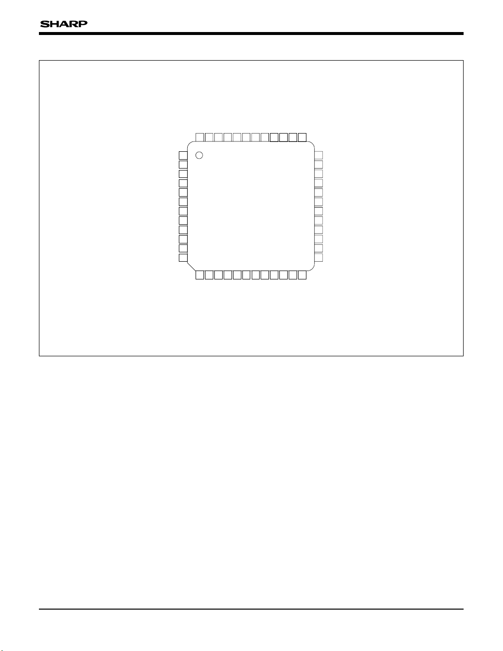
IR3Y30M/M1
2
1
48 47 4645 44 4342 41 4039 37
13 14 1516 17 1819 20 2122 23 24
2
3
4
5
6
7
8
9
10
11
12
36
35
34
33
32
31
30
29
28
27
26
25
CCD IN
CLAMP BIAS
IRIS GAMMA
WINDOW
IRIS OUT
V
CC1
GND1
EE NR
SET NR
IRIS IN
SET UP
EE UP
AGC OUT
LPF ADJ
AMP
1 IN
C
1
AGC DET
GND
2
GAMMA ADJ
KNEE ADJ
GAMMA OUT
DL ADJ
HAPA IN
APA CTRL
SYNC
BLK CLP
BCLIP
V
CC2
VIDEO OUT
PEDESTAL
WCLIP
CLAMP
2
AMP2 OUT
GAIN CTRL
C3C2
PGND
FCDSFSPVCCCDS OUT
CLAMP1AGC OP IN
MAX GAIN
AGC OP OUT
AGC CTRL
VCVREF
38
48-PIN QFP
TOP VIEW
(QFP048-P-1010)
(QFP048-P-0707)
PIN CONNECTIONS

IR3Y30M/M1
3
PGND
FS
5 V
CDS OUT AGC OP IN
AGC CTRL
VC
VREF LPF ADJ
AGC OUT AMP1 IN
AGC OP
OUT
CLAMP
1
PVcc
FCDS
CLAMP
WINDOW IRIS GAMMA
CLAMP H CLIP
AGC
OP AMP
S/H
FCDS FS
MAX GAIN
C1
GND2
AGC DET
CLP
BLK
GAMMA ADJ
KNEE ADJ
GAMMA OUT
DL ADJ
HAPA IN
APA CTRL
C
2
BCLIP
CLAMP
2
WCLIPPEDESTALBLK CLP
BLK
CLP
GND1Vcc1
EE UP
SET UP
IRIS IN
IRIS OUT BLK
SET NR
EE NR
WINDOW
WINDOW
IRIS GAMMA
CLAMP BIAS
CCD IN
CCD
Vcc
2
VIDEO OUT
SYNC
AMP2
OUT
GAIN
CTRL C3
VREF
LPF
AMP1
GAMMA
KNEE
CLEANING
CLAMP
+
–
AGC
DL
BASE
CLIP
+
+
+
+
+
–
+
–
+
–
+
–
AMP2
CLP
APA AMP
MIXCLAMP
W CLIP
SYNC
OUT
PULSE SEPA
PEDESTAL
SYNC
CLPBUFF
IRIS COMP
IRIS AMP
IRIS OP AMP
CLP
CLP
+
–
+
–
+
–
+
–
+
–
+–
39 38 37 35 36 34
33
31
32
30
29
28
27
26
25
414042434445464748
1
2
3
4
5
8
9
10
11
12
6 7 14 16 17 13 18 19 20 21 22 23 15 24
CLP
5 V5 V
BLK CLP
BLOCK DIAGRAM
IR3Y30M/M1
4
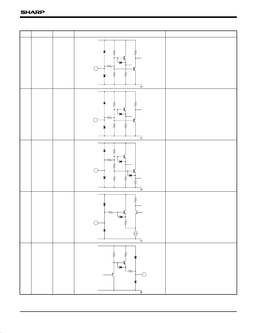
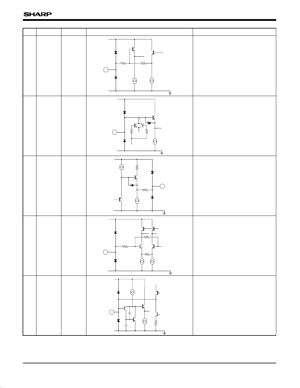
PIN DESCRIPTION
1 CCDIN
2.5 V
Input for the signal from CCD area
sensor. 2.5 V bias applied internally.
PIN NO.
PIN NAME VOLTAGE
EQUIVALENT CIRCUIT DESCRIPTION
1
25 k
200
25 k 9 k
9 k
VCC1
GND
21 k
200
29 k 9 k
9 k
VCC1
GND
2
Feed through level of the input
signal is clamped to this pin voltage.
2.9 V bias applied internally.
Connect capacitor between this pin
and GND.
2.9 V
CLAMP
BIAS
2
3
IRIS
GAMMA
3.1 V
Gamma adjustment of the exposure
circuit. This pin is preset to 3.1 V,
and gamma becomes 0.45 at open.
3
25 k
200
33.8 k 25 k
25 k
6.4 k
VCC1
GND
4
1 k
7 k
18.8 k
190 µ
VCC1
GND
Window pulse input for the exposure
circuit. Outputs the signal while "H".
WINDOW4
20 k
50
1 k
5
VCC1
GND
Output for the exposure signal.
Connect a resistor between this pin
and GND.
2.3 V
IRIS OUT5
IR3Y30M/M1
5
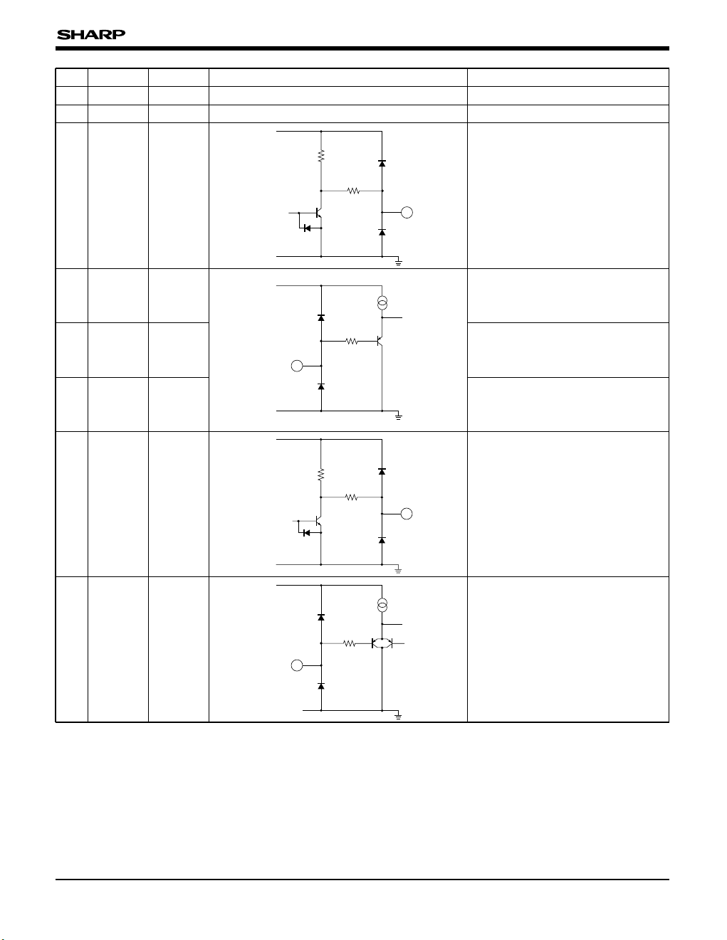
6VCC1 Power supply for analog circuits.
PIN NO.
PIN NAME VOLTAGE EQUIVALENT CIRCUIT DESCRIPTION
Ground for analog circuits.GND
17
8 EE NR
Comparator output for electronic
exposure control.
50 k
200
8
VCC1
GND
8
Input of the amplifier for electronic
exposure control. This amplifier has
5 times gain.
IRIS IN
Low reference voltage input of the
comparator for electronic exposure
control.
SET UP
200
2 µ
VCC1
GND
High reference voltage input of the
comparator for electronic exposure
control.
SET NR9
12 EE UP
Output of the comparator for
electronic exposure control.
200
50 k
12
VCC1
GND
13
5 k
40 µ
VCC1
GND
Synchronous signal input.
SYNC13
10
11
IR3Y30M/M1
6
14
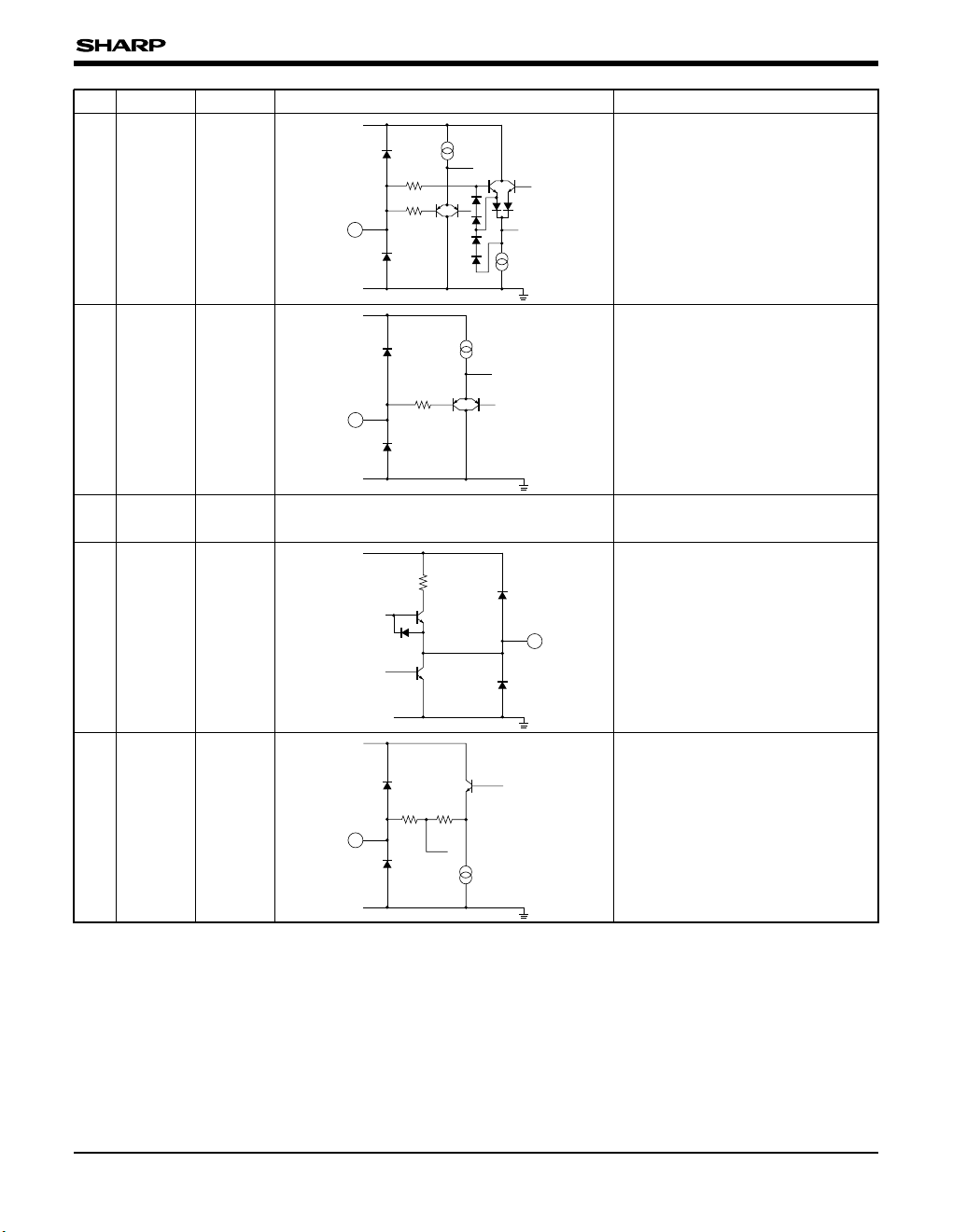
BLK CLP
Composite pulse input.
(pulse for optical black clamp and
pulse for blanking)
PIN NO.
PIN NAME VOLTAGE
EQUIVALENT CIRCUIT DESCRIPTION
14
5 k
40 µ
40 µ
5 k
VCC1
GND
15
5 k
40 µ
VCC1
GND
Adjustment for the base clip level in
the aperture circuit.
Eliminates the low-level noise of
aperture signal.
When opened, base clip is canceled.
BCLIP
15
16
V
CC2
Power supply for output amplifier
circuits.
100
17
VCC2
GND
Video signal output.
At 75 $ terminated : 1 Vp-p
(Synchronous level 0.3 Vp-p)
1.5 V
VIDEO OUT
17
18
45 k
100 µ
5 k
VCC2
GND
Blanking level adjustment.
100 mV when opened.
2.5 V
PEDESTAL
18
IR3Y30M/M1
7
19
WCLIP 3.3 V
White clip adjustment.
120% when opened.
PIN NO.
PIN NAME VOLTAGE
EQUIVALENT CIRCUIT DESCRIPTION
19
35 k
100 µ50 µ
15 k
VCC2
GND
20
50 µ
5 k
5 k
VCC2
GND
Input for encoder circuit. Black level
of input signal is clamped to 2.3 V.
2.3 VCLAMP
2
20
21
AMP2OUT
1.0 V
Output for the gain control amplifier.
21
1 m
100
50 µ
100
VCC1
GND
22
200 µ200 µ
10 k
1.8 k
39 k
VCC1
GND
Controls the output amplitude at pin
No. 21.
Gain is controlled in the range from
6 to 12 dB.
It is approximately 10 dB when this
pin is open.
2.5 V
GAIN
CTRL
22
23
50 µ
50 µ
3 p
3 p
5 k
VCC1
GND
Feedback clamp detector. Connect
capacitor between this pin and GND.
1.8 VC
3
23
 Loading...