
®
Integrated Circuits Group
ID246 Series
Flash Memory Card
(Model Numbers: ID246xxx)
Spec No.: CPS0008E-001
Product Overview
SHARI=
ID246 SERIES PRODUCT OVERVIEW
l
Handle this document carefully for it contains material protected by international copyright law. Any reproduction, full or in part, of this material is prohibited without the express written permission of the company.
l
When using the products covered herein, please observe the conditions written herein and the precautions
outlined in the following paragraphs. In no event shall the company be liable for any damages resulting from
failure to strictly adhere to these conditions and precautions.
(1) The products covered herein are designed and manufactured for the following application areas. When
using the products covered herein for the equipment listed in Paragraph (2). even for the following
application areas, be sure to observe the precautions given in Paragraph (2). Never use the products for
the equipment listed in Paragraph (3).
* Office electronics
. Instrumentation and me.asuring equipment
* Machine tools
* Audiovisual equipment
. Home appliances
* Communication equipment other than for trunk lines
(2) Those contemplating using the products covered herein for the following equipment which demands
high reliability, should first contact a sales representative of the company and then accept responsibility for incorporating into the design fail-safe operation, redundancy, and other appropriate measures for
ensuring reliability and safety of the equipment and the overall system.
* Control and safety devices for airplanes, trams, automobiles, and other transportation equipment
. Mainframe computers
- Traffic control systems
* Gas leak detectors and automatic cutoff devices
* Rescue and security equipment
. Other safety devices and safety equipment, etc.
(3) Do not use the products covered herein for the following equipment which demands extremely high
performance in terms of functionality, reliability, or accuracy.
* Aerospace equipment
. Communications equipment for trunk lines
. Control equipment for the nuclear power industry
* Medical equipment related to life support, etc.
(4) Please direct all queries and comments regarding the interpretation of the above three Paragraphs to a
sales representative of the company.
l
Please direct all queries regarding the products covered herein to a sales representative of the company.
CPS0008E-00
SHARP
ID246 SERIES PRODUCT OVERVIEW
2
1.
2.
3.
4.
5.
6.
7.
8.
9.
Contents
Intnxluction
.................................................................................................................
P.
Features
....................................................................................................................... P.
Block Diagram
............................................................................................................ P.
Pin Connections
..........................................................................................................
P.
Signal Description
......................................................................................................
P.
Functions
.....................................................................................................................
P.
6. 1 Common Memory..
.........................................................................................
P.
6. 2 Attribute Memory ................
........................................................................... P.
6. 3 Function Table
.....
.
..........................................................................................
P.
Card Information Structure (CIS)
...............................................................................
P.
Card Control
...............................................................................................................
P.
8. 1 Reset .............................................................................................................
P.
8. 2 Status Register
................................................................................................ P.
8. 3 Write Protect Switch
.......................................................................................
P.
8. 4 Identifier Codes.
..............................................................................................
P.
Component Management Register (CMR)
.................................................................
P.
10. Commad Definitions..
...............................................................................................
P.
10. 1 Query Command..
P.
.......
....................................................................................
lo. 2 STS Configuration Command
........................................................................
P.
11. Electrical Specifications
.............................................................................................
P.
11. 1 Absolute Maximum Ratings
...........................................................................
P.
11. 2 Recommended Operating Conditions.
............................................................ P.
11. 3 Capacitance
.....................................................................................................
P.
11. 4 AC Input/Output Test Conditions
..................................................................
P.
12. DC Characteristics
......................................................................................................
P.
13. AC Characteristics
...................................................................................................... P.
13. 1 Common Memory Read Operations
............................................................... P.
13. 2 Command Write Operations : Common Memory
..........................................
P.
13. 3 Attribute
Memory Read Operations
............................................................... P.
13. 4 Attribute Memory Write Operations
..............................................................
P.
13. 5 Power-Up/Power Down..
................................................................................ P.
14. Specification Changes
................................................................................................
P.
15. Other Precautions..
......................................................................................................
P.
16. External Diagrams
...................................................................................................... P.
3
3
4
5
6
7
7
8
9
9
12
12
12
12
12
15
17
18
21
22
22
22
22
22
23
25
25
27
33
34
35
36
36
37
SHARP
ID246 SERIFS PRODUCT OVERVIEW
1. Introduction
This datasheet is for SHARP’s ID246 series flash memory card. This datasheet provides all AC and DC character-
istics (including timing waveforms) and a convenient reference for the device command set and the cards integrated registers(including the Flash Memory’s status registers). This datasheet provides description of the methods which are very helpful for customer to use the card.
2. Features
2.1 Type
2.2 Overview
2.3 Interface
Flash Memory Card
Common
Byte
Memory
Capacity Word
Device
Attribute Memory
Capasity
Supply Voltage
ID246Pxx ID246Rxx
ID246Sxx
32Mbyte
40Mbyte 48Mbyte
16Mword 20Mword 24Mword
LH28F032SKD
LH28F032SKD LH28F032SKD
8devices lodevices 12devices
2Kbyte
(Note:standard CIS is not writable)
vcc=sv ! vpp=sv,
vcc=3.3v I vpp=3.3v,5v
Access time
Erase Unit
Program/Erase
Cycles
External
Dimensions
150ns(@Vcc=%)
250ns(@Vcc=3.3v)
64K word blocks
1 OO,OOOcycles/Block
PCMCIA Type 1
54.0X 85.6X 3.3mm
Parallel I/O Interface
2.4 Function Table See Function Table in page. 9
2.5 Pin Connections
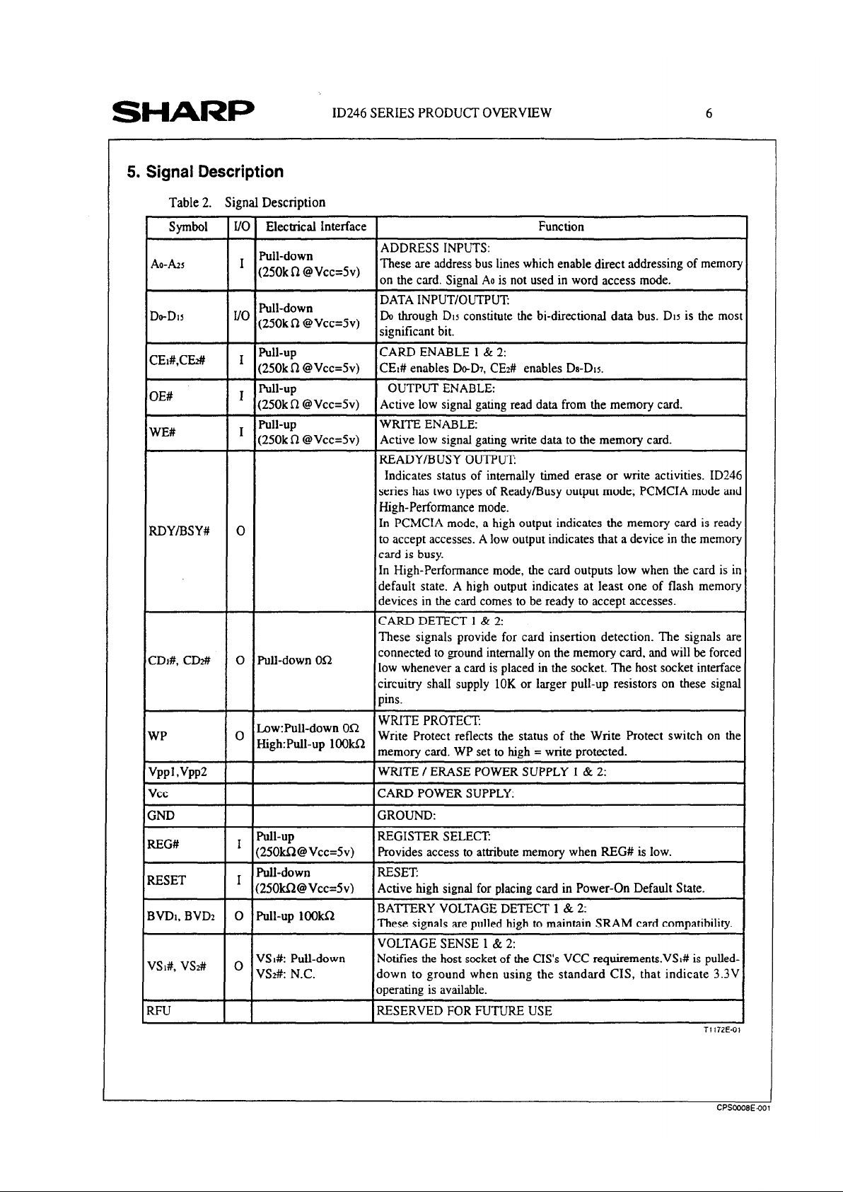
See Pin Connections in page. 5
2.6 Type of Connector
Conforms to PCMCIA PC Card Standard 95 Card Use Connector
Card connector: JC20-J68S-NB3 by JAE or
FCN-568J068-G/O by Fujitsu or
ICM-C68S-TS 13-5035A by JST
2.1 Operating Temperature 0 to 60°C
2.8 Storage Temperature -20 to 65°C
2.9
Not designed for rated radiation hardened.
SHARP
ID246 SERIES PRODUCT OVERVlEW
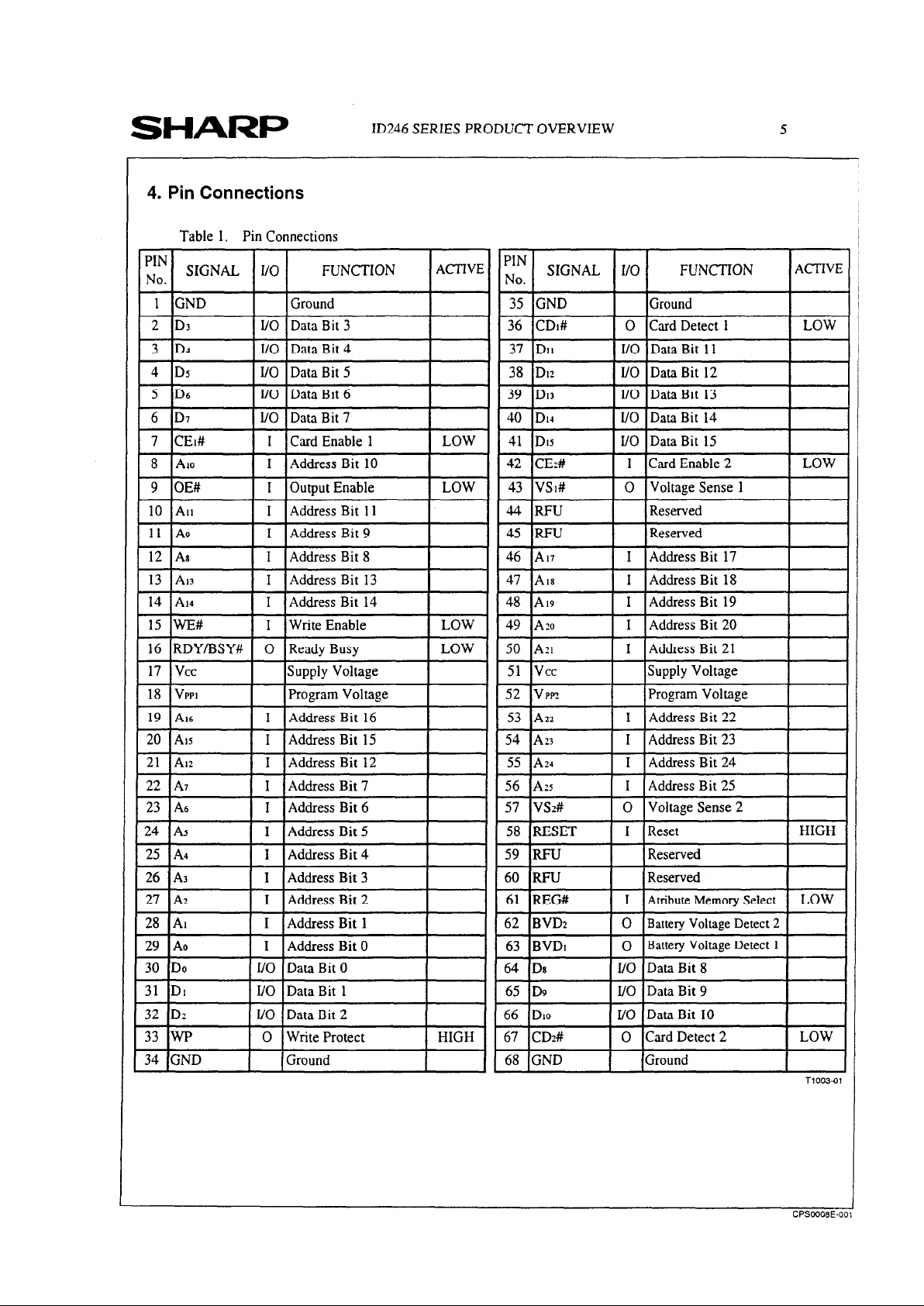
3. Block Diagram
Control
Logic
zvcc
VPPl .
VPP2 ~
: :
:
I I I I
:
:
.
m
’ ’ - - - -
- - - -
VPP2 vcc
VPP 1 vcc
t t
Flash Memory Flash Memory
3 Data wP#k+ -bwP#
Data *’
.
e Add cE#l* + cm
Add 4
-Rp#
A
wE# 4---,
*WI3
RPWJ
STS OE# M
- OE#
STS -
/A
VPP2
t /I
vcc
VPP2
vcc
Flash Memory
b Data
wFJ# 4---
b Add cE# 4--**
wE# 4---(c
- STS
OE# 4i()--
Flash Memory
l w
Data * - -
+ cE#
Add + - -
l wE# RP#-+
* OE#
STS ---( ’
Figure 1. Block Diagram
SHARP
ID246 SERIES PRODUCT OVERVIEW
5
4. Pin Connections
Table 1. Pin Connections
T
I I
;r
SIGNAL I/O
I I
FUNCTION
ACTIVE
4
I I
;,” SIGNAL I/O
I I
FUNCTION
ACTIVE
LOW
LOW
HIGH
LOW
LOW
T1003-01
I
I
40 ~D,J
39 DIG
I I I
1 I/O IData Bit 14
1 I/O IData Bit 13
5 D6
6
D7
I/O Data Bit 6
I/O Data Bit 7
41 DIG
42 CEz#
I/O Data Bit 15
I Card Enable 2
7 CEI#
8 AIO
I Card Enable 1
I Address Bit 10
43 VSI#
44 RFU
0 Voltage Sense 1
Reserved
9 OE#
10 Al1
I Output Enable
I Address Bit 11
1 11 1As I I IAddress Bit9
I I 45 Imu
1 IReserved
I 1 1
15 IWE# I I I Write Enable
I
I
I I 1 Address Bit 20
I 16 IRDYTSSY# I o IReady
BUSY
LOW 1 1 50 IAx I I IAddress Bit 21
17 vcc
18
VPPI
Supply Voltage
Program Voltage
1 22
IA7
I I IAddress Bit7 1 1 56 IA25 I 1 (Address Bit 25
1 1 57 IVS2# I 0 IVoltage Sense 2 23 As
24 As
I Address Bit 6
I Address Bit 5 1 1 58 IkESET I I (Reset
25 A4
26 As
I Address Bit 4
I [Address Bit 3
-II
62 63 (BVD2 IBVD~
I 0 0 Battery Battery
Voltage Voltage Detect Detect 2
1
I 30 (Do I I/O (Data Bit 0
1 I/O (Data Bit 8
1 34 (GND
I
1 Ground
1 1
68
(GND
I
(Ground
I
CPSOQ08E.001
SHARP
ID246 SERIES PRODUCT OVERVIEW 6
1
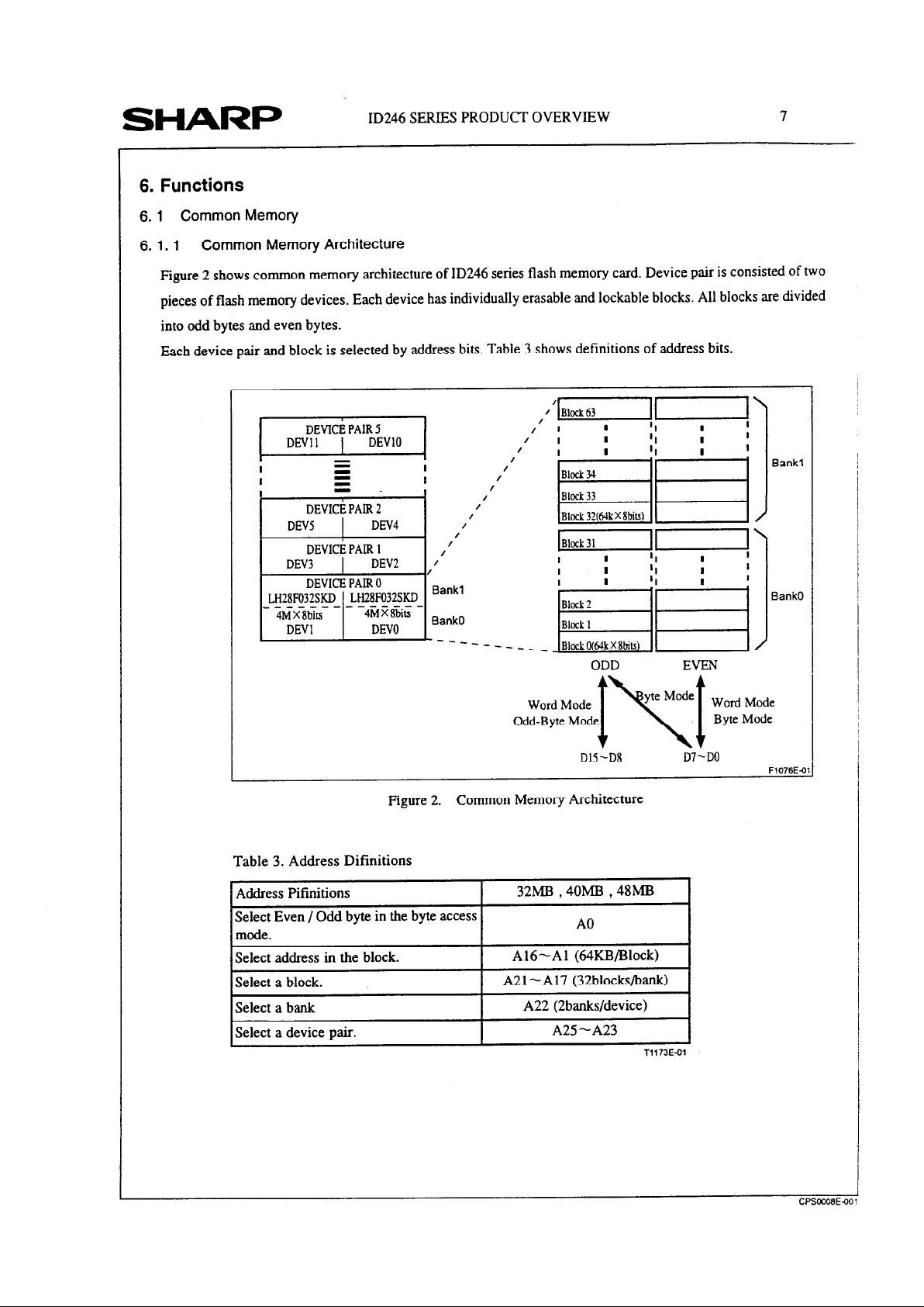
5. Signal Description
Table 2. Signal Description
Function
ADDRESS INPUTS:
40425
These are address bus lines which enable direct addressing of memory
on the card. Signal Ao is not used in word access mode.
DATA INPUT/OUTPUT
Do through DIG constitute the bi-directional data bus. Drs is the most
significant bit.
,,. Pull-down
I
(250kn @Vcc=Sv)
h-D15
CARD ENABLE 1 & 2:
CEI# enables D+D7, CE2# enables Da-DIG.
:Ei#,CEz#
>E#
OUTPUT ENABLE:
Active low signal gating read data from the memory card.
WRITE ENABLE:
Active low signal gating write data to the memory card.
READY/BUSY OUTPUp
NE#
Indicates status of internally timed erase or write activities. ID246
series has two types of Ready/Busy output mode; PCMCIA mode and
High-Performance mode.
In PCMCIA mode, a high output indicates the memory card is ready
to accept accesses. A low output indicates that a device in the memory
card is busy.
In High-Performance mode, the card outputs low when the card is in
default state. A high output indicates at least one of flash memory
devices in the card comes to be ready to accept accesses.
CARD DETECT 1 & 2:
0
IDYlBSY#
:DI#, CDz#
These signals provide for card insertion detection. The signals are
connected to ground internally on the memory card, and will be forced
low whenever a card is placed in the socket. The host socket interface
circuitry shall supply 10K or larger pull-up resistors on these signal
pins.
WRITE PROTECT:
0 Pull-down Of2
t
o Low:PuIl-down On
High:Pull-up 1OOkn
Write Protect reflects the status of the Write Protect switch on the
memory card. WP set to high = write protected.
I
VP
WRITE / ERASE POWER SUPPLY 1 & 2:
I
(PPI .VPP2
[cc CARD POWER SUPPLY:
I
iND
GROUND:
I
EG#
REGISTER SELECT:
Provides access to attribute memory when REG# is low.
RESET
Active high signal for placing card in Power-On Default State.
BATTERY VOLTAGE DETECT 1 & 2:
These signals are pulled high to maintain SRAM card compatibility.
VOLTAGE SENSE 1 & 2:
ESET
;VDI, BVDz 0 Pull-up 1ookQ
I
Notifies the host socket of the CIS’s VCC requirements.VS~# is pulledlawn to ground when using the standard CIS, that indicate 3.3V
operating is available.
RESERVED FOR FUTURE USE
T1172E.01
o VSI#: Pull-down
I
VS2#: N.C.
'Sl#, vs2#
CPS0008E40'
SHARI=
ID246 SERIES PRODUCT OVERVIEW
7
6. Functions
6.1 Common Memory
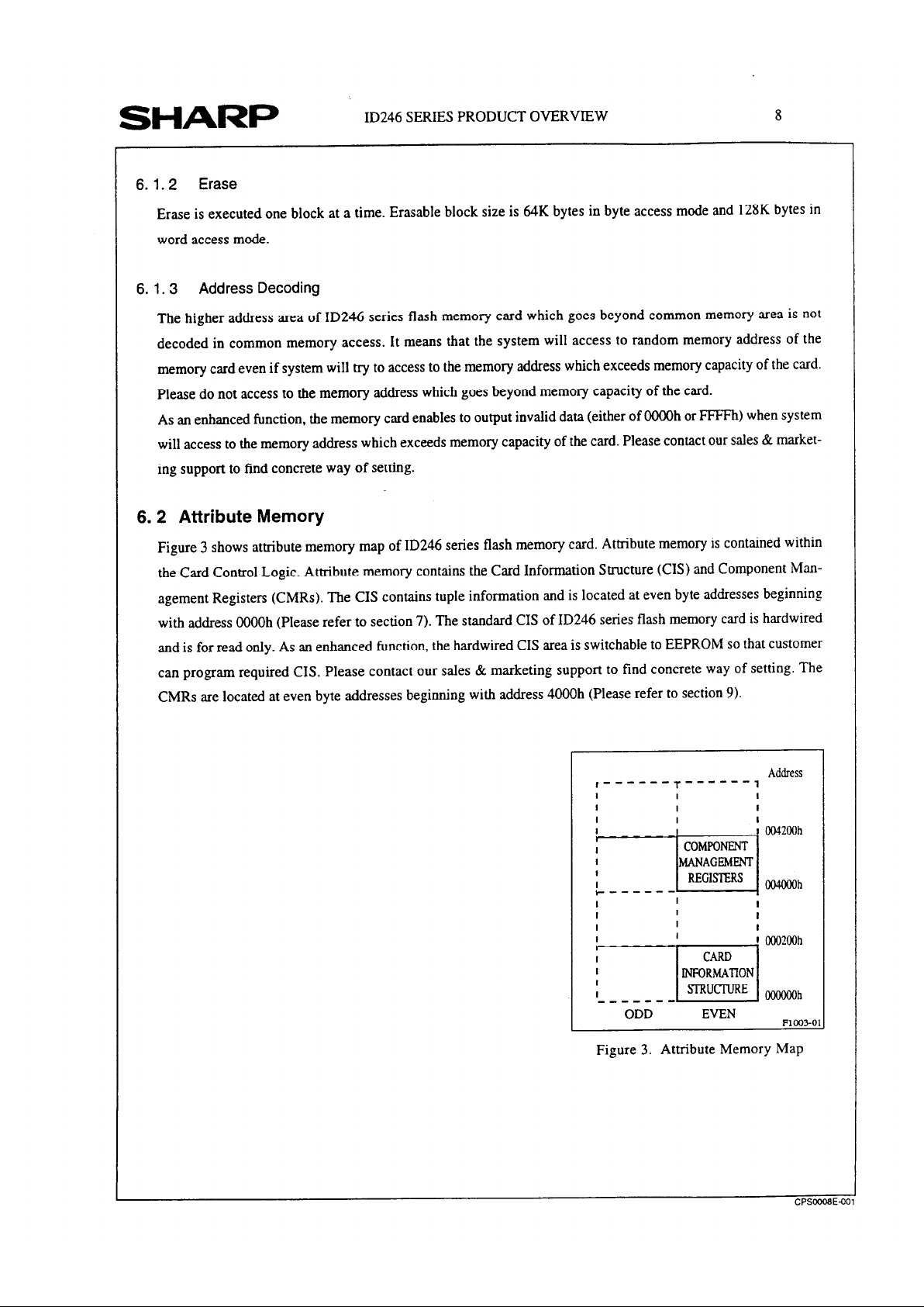
6. 1. 1 Common Memory Architecture
Figure 2 shows common memory architecture of ID246 series flash memory card. Device pair is consisted of two
pieces of flash memory devices. Each device has individually erasable and lockable blocks. All blocks are divided
into odd bytes and even bytes.
Each device pair and block is selected by address bits. Table 3 shows definitions of address bits.
DEVICE PAIR 5
DEVll 1 DEVIO
=
=
=
DEVICi PAIR 2
DEVS 1 DEV4
DEVIti PAIR 1
DEV3 1 DEV2
I
DEVICE PAIR 0
LH28FO32SKD LH28FO32SKD
- jGx-8&- - - -4;I z 8jjii DEVl DEVO
/
/
Bank1
Bank0
/’ Blodc63
/
/ 1
I
‘W
‘I I
/
I
I
‘I
I
I
1
Bank1
1
Bank0
ODD
EVEN
Word Mode
yte Mode
I\1
Word Mode
Odd-Byte Mode
Byte Mode
D15-D8 D7-DO
F1076E4)’
Figure 2. Common Memory Architecture
Table 3. Address Difinitions
Address Pifinitions 32MB ,4OMB ,48MB
Select Even / Odd byte in the byte access
A0
mode.
Select address in the block. A16-Al (64KJ3/Block)
Select a block.
A21 -A17 (32blocks/bank)
Select a bank
A22 (2banks/device)
Select a device pair. A25 -A23
T1173E-01
SHARI=
ID246 SERIES PRODUCT OVERVIEW
8
6. 1.2 Erase
Erase is executed one block at a time. Erasable block size is 64K bytes in byte access mode and 128K bytes in
word access mode.
6. 1.3 Address Decoding
The higher address area of ID246 series flash memory card which goes beyond common memory area is not
decoded in common memory access. It means that the system will access to random memory address of the
memory card even if system will try to access to the memory address which exceeds memory capacity of the card.
Please do not access to the memory address which goes beyond memory capacity of the card.
As an enhanced function, the memory card enables to output invalid data (either of OOOOh or FFFFh) when system
will access to the memory address which exceeds memory capacity of the card. Please contact our sales & marketing support to find concrete way of setting.
6.2 Attribute Memory
Figure 3 shows attribute memory map of ID246 series flash memory card. Attribute memory is contained within
the Card Control Logic. Attribute memory contains the Card Information Structure (CIS) and Component Management Registers (CMRs). The CIS contains tuple information and is located at even byte addresses beginning
with address OOOOh (Please refer to section 7). The standard CIS of ID246 series flash memory card is hardwired
and is for read only. As an enhanced function, the hardwired CIS area is switchable to EEPROM so that customer
can program required CIS. Please contact our sales & marketing support to find concrete way of setting. The
CMRs are located at even byte addresses beginning with address 4000h
(Please refer to section 9).
Address
,-“--’ T--“-‘,
ODD
EVEN
F1003-01
Figure 3. Attribute Memory Map
SHARP
ID246 SERIES PRODUCT OVERVIBW
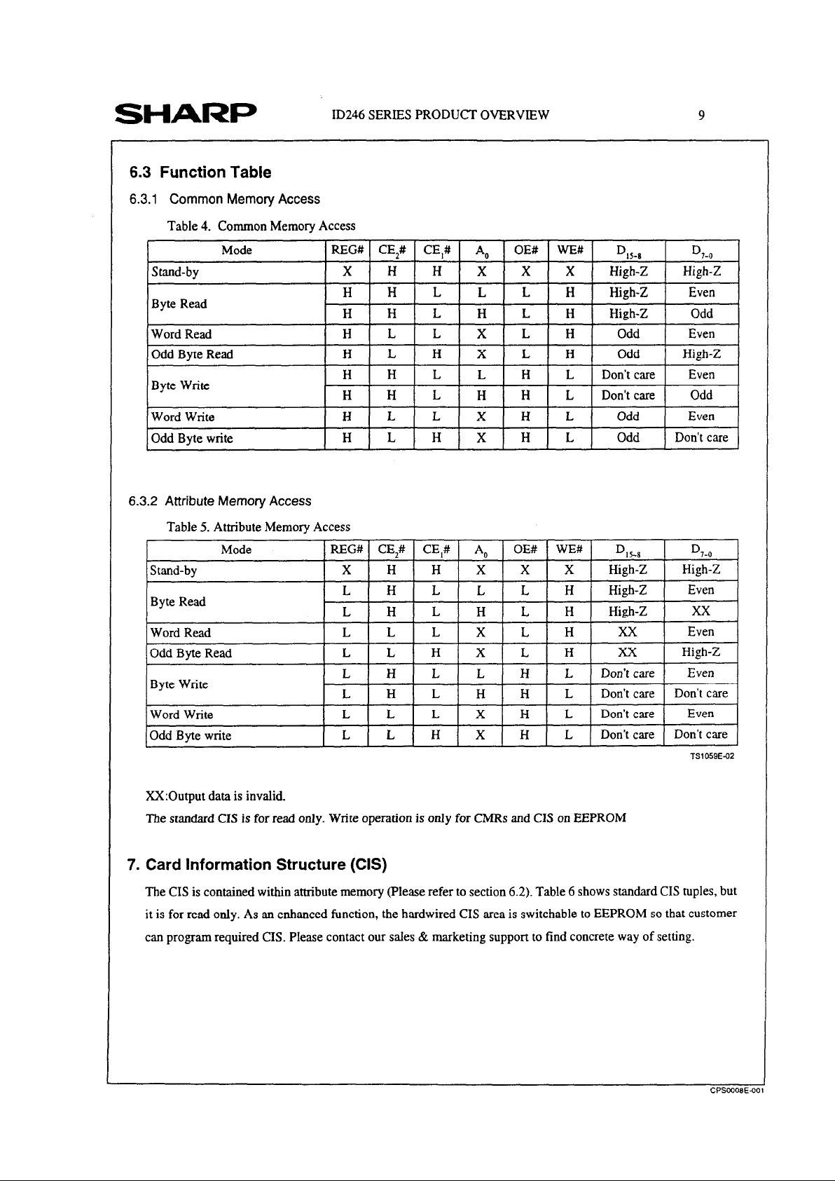
6.3 Function Table
6.3.1 Common Memory Access
Table 4. Common Memory
Mode
Stand-by
Byte Read
Word Read
Odd Byte Read
Byte Write
Word Write
Odd Byte write
tcess
H H L H H L Don’t care Odd
H L L X H L Odd Even
H L H X H L Odd Don’t care
6.3.2 Attribute Memory Access
Table 5. Attribute Memory Access
Mode REG# CE,# CE,# A, OE# WE# D,,, D
7-o
Stand-by
X H H X X X High-Z High-Z
L H L L L H
Even
Byte Read
High-Z
L H L H L H
High-Z xx
Word Read L L L X L H
xx Even
Odd Byte Read
Byte Write
Word Write
Odd Byte write
L L H X L H xx
High-Z
L H L L H L Don’t care
Even
L H L H H L
Don’t care Don’t care
L L L X H L Don’t care
Even
L L H X H L Don’t care
Don’t care
TS1059E-02
XX:Output data is invalid.
The standard CIS is for read only. Write operation is only for CMRs and CIS on EEPROM
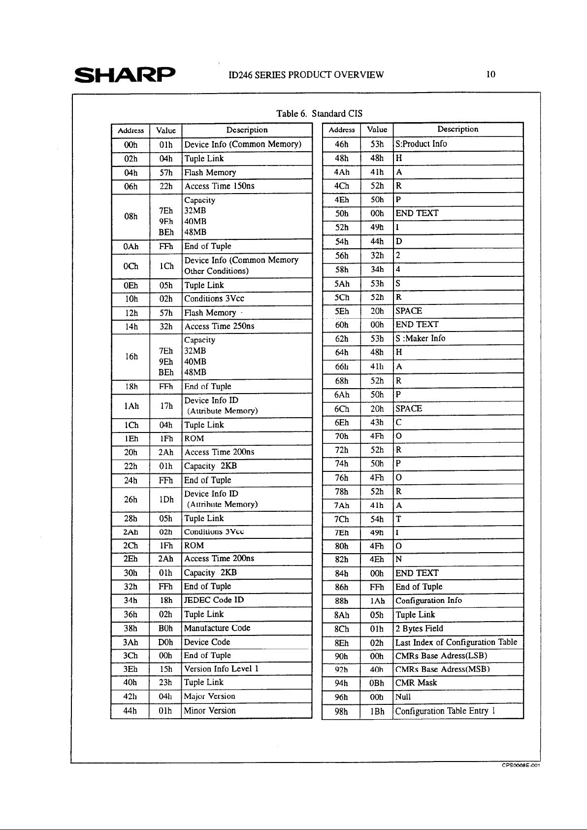
7. Card Information Structure (CIS)
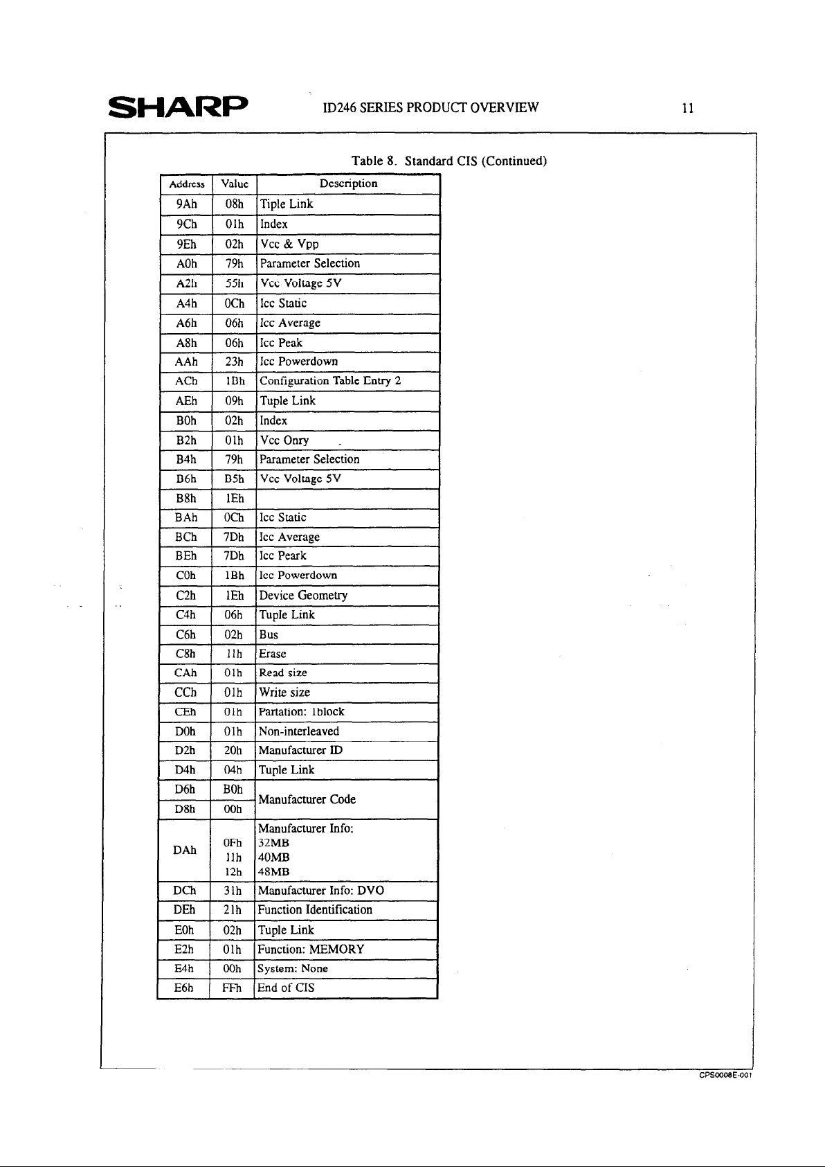
The CIS is contained within attribute memory (Please refer to section 6.2). Table 6 shows standard CIS tuples, but
it is for read only. As an enhanced function, the hardwired CIS area is switchable to EEPROM so that customer
can program required CIS. Please contact our sales & marketing support to find concrete way of setting.
SHARP
ID246 SERIES PRODUCT OVERVIEW
Table 6. Standard CIS
Address
1 Value 1
Description
I
1 Address 1 Value
1 OOh 1 Olh
, 02h / 04h -1
1 46h 1 53h ISProduct Info
I
48h
4Ah
48h H
41h A Rash Memory
I
Access Time 150ns 4Ch 52h R
4Eh 50h P
I I
08h
7Eh
9Eh
Capacity
32MB
40MB
50h
52h
54h
56h
OOh END TEXT
4Yh I
4th D
32h 2
58h
34h 4
5Ah 53h S
5Ch
52h R
5Eh 20h SPACE
10h
12h
02h Conditions 3Vcc
57h Flash Memory
48h H
41h A
52h R
6Ah 1 50h IP
6Ch 1 20h ISPACE
60h
62h
64h
66h
6Xh
OOh ENDTEXT
53h S :Maker Info
Access Time 250ns
Capacity
32MB
40MB
48MB
End of Tuple
I I
1Ch
04h Tuple Link
I
43h C
4I=h 0
72h 1 52h IR
74h I 50h IP
6Eh
70h
1Eh ( 1Ph IROM
I
Access Time 200ns
Capacity 2KB
76h 1 4Fh 0
78h i 52h IR
End of Tuule
7Ah ( 41h A
7Ch 1 54h IT
28h 05h Tuple Link
2Ah 1 02h IConditions 3Vcc
ROM 1 2Cb 1 1Ph
7Eh
80h
82h
84h
86h
88h
8Ah
49h I
4I=h 0
4Eh N
OOh END TEXT
PFh End of Tuple
1 Ah Configuration Info
05h Tuple Link
2Eh
30h
32h
34h
36h
38h
3Ah
2Ab Access Time 2OOr-r~
Olh Capacity 2KB
PI% End of Tuple
18h JEDEC Code ID
02h Tuple Link
BOh Manufacture Code
DOh Device Code
Last Index of Configuration Table
3Ch
OOh End of Tuple
3Eh
15h Version Info Level 1
40h
23h Tuple Link
42h 04h Major Version
44h Olh Minor Version
CPS0008E401
SHARP
ID246 SERIES PRODUCT OVERVIEW
Table 8. Standard CIS (Continued)
Address
1 Value 1 Description
I
9Ah
08h Tiple Link
9Ch
Olh Index
9Eh
02h
vcc & vpp
AOh
A2h
A4h
79h Parameter Selection
55h Vcc Voltage 5V
OCh ICC Static
A6h
A8h
06h ICC Average
06h ICC Peak
AAh 23h ICC Powerdown
ACh 1 1Bh 1 Contieuration Table Entrv 2 I
AEh
BOh
09h Tuple Link
02h Index
B2h
B4h
Olh Vcc Onry
79h Parameter Selection
B6h
B8h
B5h Vcc Voltage 5V
1Eh
BAh
BCh
BEh
OCh ICC Static
7Dh ICC Average
7Dh ICC Peark
COh 1 1Bh (ICC Powerdown
I
C2h
C4h
1Eh Device Geometry
06h Tuple Link
C6h 1 02h Bus
C8h 1 llh IErase
CAh ) Olh IRead size
I
CCh
CEh
Olh Write size
Olh Partation: lblock
DOh
D2h
0 1 h Non-interleaved
20h Manufacturer ID
D4h 1 04h ITunle Link
I
-+E-ta
Manufacturer Code
DEh
EOh
2 1 h Function Identification
02h Tuple Link
E2h
E4h
0 1 h Function: MEMORY
OOh System: None
E6h FFh End of CIS
I
CPS0008E-00
 Loading...