

GP1A35RV
GP1A35RV
High Sensing Accuracy OPIC
Photointerrupter with
Encoder Functions
■ Features
1. 2-phase (A, B) digital output
2. High sensing accuracy
(Disk slit pitch: 0.22mm, Moire stripe appli-
cation
)
3. TTL compatible output
4. Compact and light
■ Applications
1. Copiers
2. Electronic typewriters, printers
3. Numerical control machines
15.0
8.8
20.2
1A35R
±
0.15
(
Unit : mm
6
5
4
3
OPIC
4 V
OB
5 GND
6 V
CC
4.0
4-R1.4
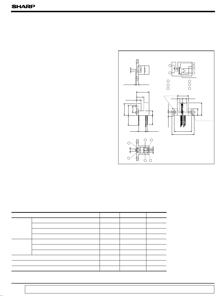
■ Outline Dimensions
0.1
0.8
11.4
3.9
MIN.
10.0
±
9.9
2- φ 2.0
±
2
)
2.54
(
1
0.15
+ 0.1
- 0.2
0.15
±
(
7.08
6.4
)
7.3
2.0
12.0
+ 0.15
- 0.1
OPIC
±
0.15
(
1.27
34
56
4.4
MIN.
8.0
)
)
1.27
(
3 -
Internal connection diagram
1
2
1 Anode
2 Cathode
3 V
OA
4 - R2.6
2.0
0.15
±
1.4
0.15
±
2.5
*Tolerance:± 0.3mm
*( ): Reference dimensions
*“ OPIC” (Optical IC) is a trademark of the SHARP Corporation.
An OPIC consists of a light-detecting element and signal processing circuit integrated onto a single chip.
6.4
12.0
±
)
0.15
■ Absolute Maximum Ratings
(
Ta= 25˚C
)
Parameter Symbol Rating Unit
Input
Forward current I
*1
Peak forward current I
Reverse voltage V
F
FM
R
65 mA
1A
6V
Power dissipation P 100 mW
Supply voltage V
Output
Low level output current I
Power dissipation P
Operating temperature T
Storage temperature T
*2
Soldering temperature T
CC
OL
O
opr
stg
sol
*1 Pulse width<=100µ s, Duty ratio= 0.01 *2 For 5 seconds
“ In the absence of confirmation by device specification sheets, SHARP takes no responsibility for any defects that occur in equipment using any of SHARP's devices, shown in catalogs,
data books, etc. Contact SHARP in order to obtain the latest version of the device specification sheets before using any SHARP's device.”
7V
20 mA
250 mW
0 to + 70 ˚C
- 40 to + 80 ˚C
260 ˚C
GP1A35RV
■ Electro-optical Characteristics
Parameter Symbol Conditions MIN. TYP. MAX. Unit
Input
Output
Forward voltage V
Reverse current I
High level V
Low level V
High level V
Low level V
Output
voltage
Phase A
Phase B
Dissipation current I
Transfer
charac-
teristics
*3 In the condition that output A and B are low level.
*5 θ
AB1
Duty ratio
Phase difference 50 90 130 deg.
Response speed
t
AB1
= x 360˚
t
AP
■ Output Waveforms
Output A
)
(V
OA
Output B
)
(V
OB
Rotational direction: Counterclockwise when seen
t
AH
t
AP
t
t
BH
AB1
t
BP
from OPIC light detector
IF= 30mA - 1.2 1.5 V
F
VR=3V - - 10 µA
R
VCC= 5V, IF= 30mA 2.4 4.9 -
AH
IOL= 8mA, IF= 30mA, VCC=5V
AL
VCC= 5V, IF= 30mA 2.4 4.9 -
BH
IOL= 8mA, IF= 30mA, VCC=5V
BL
*3
VCC= 5V, IF= 30mA
CC
*4
*4
*5
I
∆
∆
θ
AB1
t
r
t
f
= 30mA
F
A
*6
f= 12kHz
B
V
=5V
CC
IF= 30mA, VCC= 5V - 1.0 2.0
*6
f= 12kHz
t
*4 ∆A= x 100, ∆B= x100
AH
t
AP
t
BH
t
BP
- 0.1 0.4
- 0.1 0.4
- 5 20 mA
30 50 70 %
- 1.0 2.0
*6 Measured under the condition shown in Measurement Conditions.
(
Ta= 25˚C
)
V
µ s
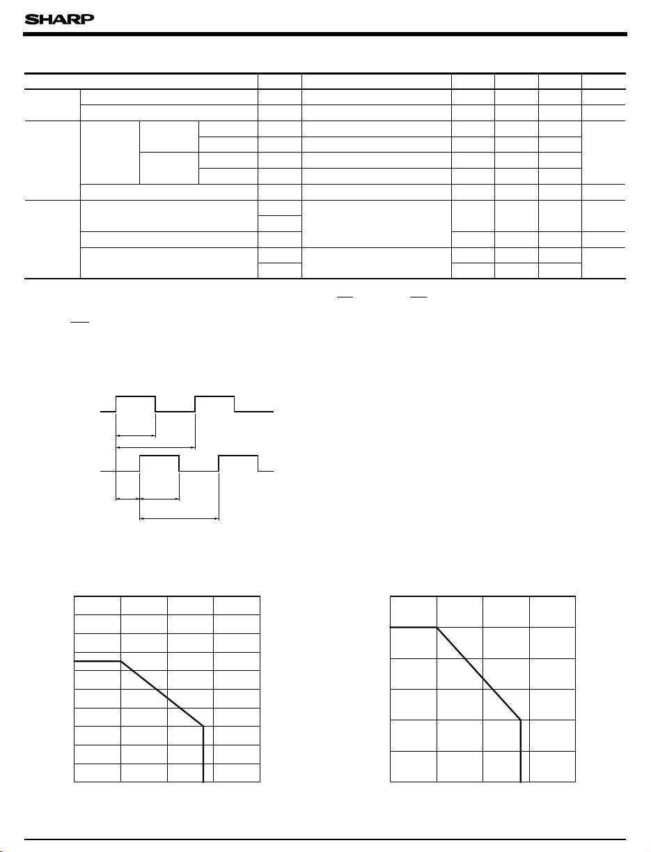
Fig. 1 Forward Current vs. Ambient
Temperature
100
90
80
)
70
mA
(
65
F
60
50
40
30
Forward current I
20
10
0
0
25 50 75 100
Ambient temperature Ta (˚C
70
)
Fig. 2 Output Power Dissipation vs.
Ambient Temperature
300
250
)
mW
(
o
200
150
100
50
Output power dissipation P
0
0
Ambient temperature T
70
(˚C
a
100755025
)

GP1A35RV
Fig. 3 Duty Ratio vs. Frequency
0.9
0.8
0.7
0.6
0.5
Duty ratio
0.4
0.3
0.2
0.1
Frequency f (kHz
VCC=5V
= 30mA
I
F
T
= 25˚C
a
t
AH
(
)
Output A
t
AP
t
BH
(
)
Output B
t
BP
52
101
20
)
Fig. 5 Duty Ratio vs. Ambient Temperature
1.0
0.9
0.8
0.7
0.6
0.5
Duty ratio
0.4
0.3
0.2
0.1
0
0
t
AH
(
Output A
t
AP
t
BH
(
Output B
t
BP
25
Ambient temperature T
)
)
a
(˚C
VCC=5V
= 30mA
I
F
f= 12kHz
)
1007550
Fig. 7 Duty Ratio vs. Distance (Xdirection
0.9
0.8
0.7
0.6
0.5
Duty ratio
0.4
0.3
0.2
0.1
- 0.5- 1.0
0 1.0
Distance X (mm) (Shifting encoder
VCC=5V
= 30mA
I
F
f= 12kHz
a
T
= 25˚C
t
AH
(
)
Output A
t
AP
t
BH
(
)
Output B
t
BP
0.5
)
Fig. 4 Phase Difference vs. Frequency
130
VCC=5V
120
I
= 30mA
F
)
= 25˚C
T
a
110
deg.
(
AB1
100
90
80
Phase difference θ
70
θ
= x 360˚
AB1
t
AB1
t
AP
60
50
1
52
Frequency f (kHz
)
2010
Fig. 6 Phase Difference vs. Ambient
Temperature
140
130
)
120
deg.
(
110
AB1
100
90
80
70
Phase difference θ
t
θ
= x360˚
AB1
AB1
t
AP
60
50
40
0
25
50 75 100
Ambient temperature Ta (˚C
)
Fig. 8 Phase Difference vs.
Distance (Xdirection
140
VCC=5V
= 30mA
I
F
130
f= 12kHz
)
T
= 25˚C
a
120
deg.
(
AB1
110
100
90
Phase difference θ
80
70
60
t
AB1
θ
= x360˚
AB1
t
AP
- 0.5- 1.0
Distance X (mm) (Shifting encoder
VCC=5V
= 30mA
I
F
f= 12kHz
)
)
Reference position
(-)(
)
+
GP1A35RV
)
Disk
1.00.50

GP1A35RV
Fig. 9 Duty Ratio vs. Distance (Ydirection
0.9
0.8
0.7
0.6
0.5
Duty ratio
0.4
0.3
0.2
0.1
- 0.5- 1.0
Distance Y (mm) (Shifting encoder
VCC=5V
= 30mA
I
F
f= 12kHz
T
= 25˚C
a
t
AH
(
)
Output A
t
AP
t
BH
(
)
Output B
t
BP
1.00.50
)
Fig.11 Duty Ratio vs. Distance (Zdirection
0.8
VCC=5V
= 30mA
I
F
0.7
f = 12kHz
T
= 25˚C
a
0.6
0.5
0.4
Duty ratio
0.3
0.2
0.1
0
0
Distance Z (mm) (Shifting encoder
t
AH
(
)
Output A
t
AP
t
BH
(
)
Output B
t
BP
0.9 1.0
0.80.70.60.50.40.30.20.1
)
)
Fig.10 Phase Difference vs.
Distance (Ydirection
130
120
)
deg.
(
AB1
110
100
t
θ
= x360˚
AB1
AB1
t
AP
)
=5V
V
CC
= 30mA
I
F
f= 12kHz
Ta= 25˚C
90
θ
=x 360 ˚
AB1
GP1A35RV
)
t
AB1
t
AP
(+)
Reference
position
(-)
Disk
)
1.00.50
80
Phase difference θ
70
60
50
- 0.5- 1.0
Distance Y (mm) (Shifting encoder
)
Fig.12 Phase Difference vs.
Distance (Zdirection
140
VCC=5V
= 30mA
I
F
130
f= 12kHz
)
T
= 25˚C
a
120
deg.
(
110
AB1
100
90
80
Phase difference θ
70
60
0
0.1 0.2 0.3 0.4 0.5 0.6 0.7 0.8
Distance Z (mm) (Shifting encoder
(
Detecting side
Z
(
Emitting side
OPIC
)
Disk
)
1.00.9
)

GP1A35RV
Measurement Conditions
0.9 ˚(Number of slit : 400
0.45 ˚
R14
3.8
X
R16.5
Disk center
Note 2
)
)
Note 1
0.3
12.86
20.8
8.8
A
1A35R
(
12.0
Note 1) Distance between disk surface and case surface in the detector side is 0.3mm.
2) Encoder positioning pin is positioned on X-X' axis.
Distance between center of disk and portion A of positioning pin is 12.86mm.
3) Center of disk slit is R14.0.
4-R1.4
1.4
6.4
)
9.9
)
15
X'
3.9
20.2
12
7.3
■ Precautions for Use
(1) This module is designed to be operated at IF= 30mA TYP.
(2) Fixing torque : MAX. 0.6N • m
(3) In order to stabilize power supply line, connect a by-pass capacitor of more than 0.01µF
between Vcc and GND near the device.
(4) As for other general cautions, refer to the chapter “ Precautions for Use”.
■ Application Circuit (Detection of Rotational Direction
A
M
GP1A35RV
output
B output
R
C
QQD
T
Q
1
Q'
)
Q
3
DQQTDQQ
T
1
Q
2
Q
4
Detection signal of
rotational direction
Q'
3
C • C • W
C • W
When gate delay causes pulse noise in Q4 output,
apply the CR filter to remove pulse noise.
 Loading...