

Page 1
CD-DVD500
SERVICE MANUAL
No. S8154CDDVD500
DVD MINI COMPONENT SYSTEM
MODEL CD-DVD500
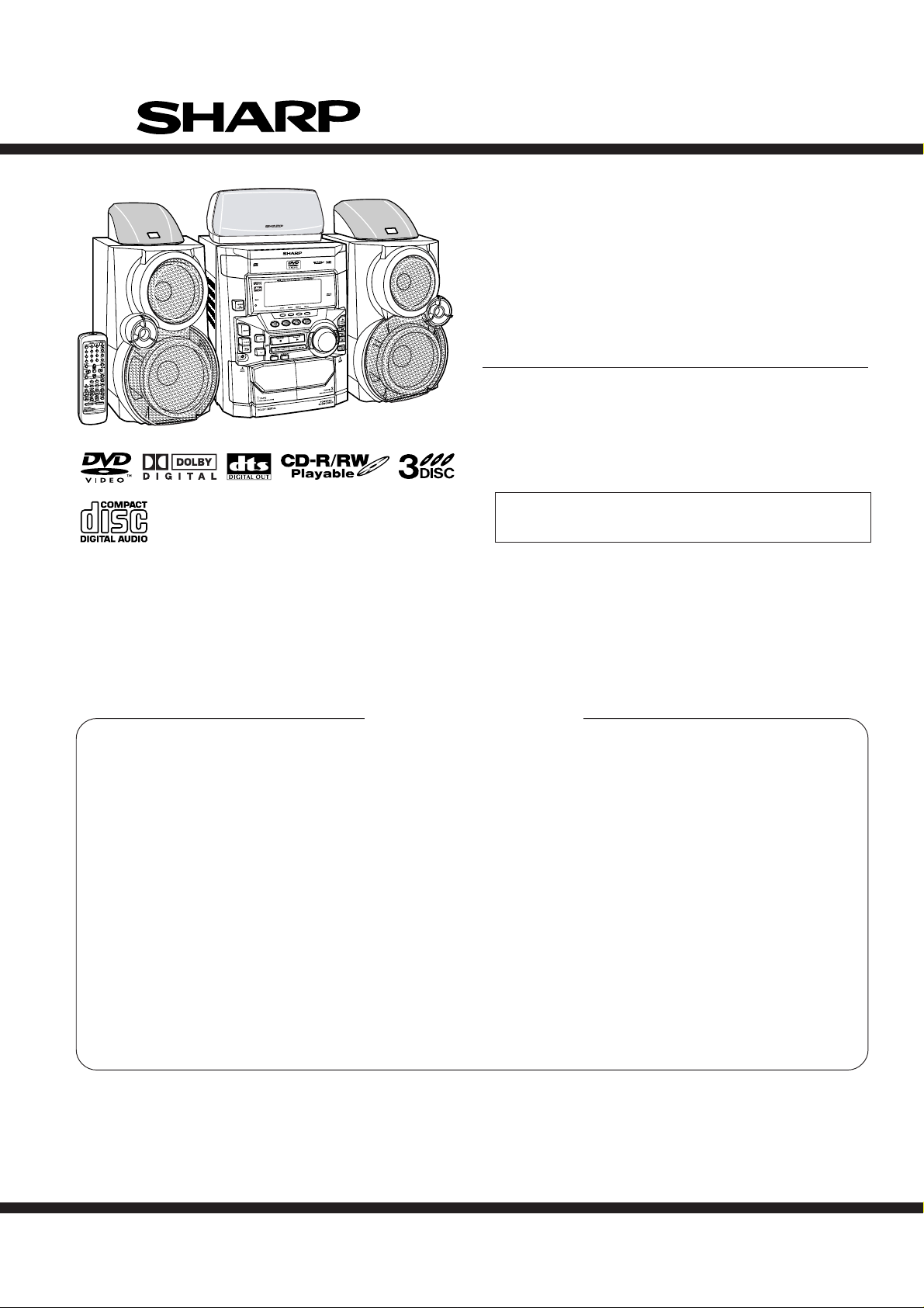
CD-DVD500 DVD Mini Component System consisting of
CD-DVD500 (main unit), CP-DVD500 (front speaker),
GBOXS0064AWM4 (center speaker), GBOXS2008AWM4
(right surround speaker) and GBOXS4008AWM4 (left
surround speaker).
• In the interests of user-safety the set should be restored to its
original condition and only parts identical to those specified be
used.
CONTENTS
Page
IMPORTANT SERVICE NOTES (FOR U.S.A. ONLY)....................................................................................................... 2
SPECIFICATIONS ............................................................................................................................................................. 2
NAMES OF PARTS ........................................................................................................................................................... 3
OPERATION MANUAL ...................................................................................................................................................... 6
DISASSEMBLY................................................................................................................................................................ 12
REMOVING AND REINSTALLING THE MAIN PARTS................................................................................................... 15
ADJUSTMENT ................................................................................................................................................................. 16
BLOCK DIAGRAM ........................................................................................................................................................... 22
SCHEMATIC DIAGRAM / WIRING SIDE OF P.W.BOARD..............................................................................................26
NOTES ON SCHEMATIC DIAGRAM .............................................................................................................................. 56
TYPES OF TRANSISTOR AND LED................................................................................................................................56
VOLTAGE ........................................................................................................................................................................ 57
WAVEFORMS OF DVD CIRCUIT ................................................................................................................................... 58
TROUBLESHOOTING ..................................................................................................................................................... 59
FUNCTION TABLE OF IC................................................................................................................................................ 62
FL DISPLAY......................................................................................................................................................................81
REPLACEMENT PARTS LIST/EXPLODED VIEW
PACKING OF THE SET (FOR U.S.A. ONLY)
SHARP CORPORATION
– 1 –
This document has been published to be used
for after sales service only.
The contents are subject to change without notice.
Page 2
CD-DVD500
FOR A COMPLETE DESCRIPTION OF THE OPERATION OF THIS UNIT, PLEASE REFER
TO THE OPERATION MANUAL.
IMPORTANT SERVICE NOTES (FOR U.S.A. ONLY)
BEFORE RETURNING THE AUDIO PRODUCT
(Fire & Shock Hazard)
Before returning the audio product to the user, perform the
following safety checks.
1. Inspect all lead dress to make certain that leads are not
pinched or that hardware is not lodged between the chassis
and other metal parts in the audio product.
2. Inspect all protective devices such as insulating materials,
cabinet, terminal board, adjustment and compartment covers
or shields, mechanical insulators etc.
3. To be sure that no shock hazard exists, check for leakage
current in the following manner.
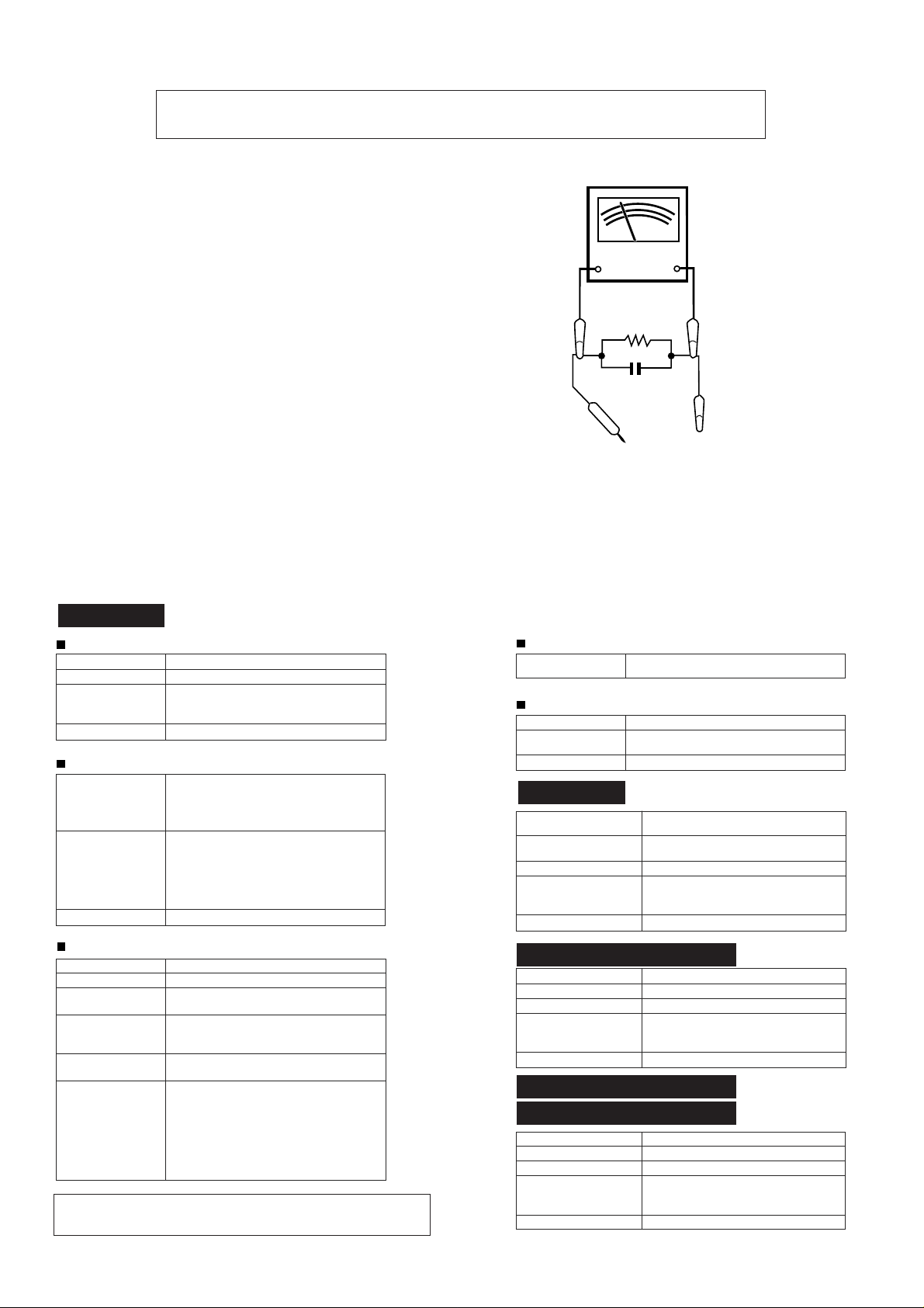
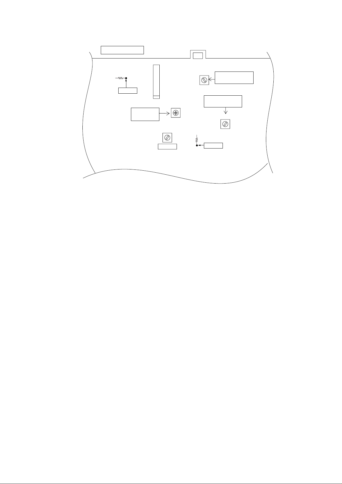
* Plug the AC line cord directly into a 120 volt AC outlet.
* Using two clip leads, connect a 1.5k ohm, 10 watt resistor
paralleled by a 0.15µF capacitor in series with all exposed
metal cabinet parts and a known earth ground, such as
conduit or electrical ground connected to earth ground.
* Use a VTVM or VOM with 1000 ohm per volt, or higher,
sensitivity to measure the AC voltage drop across the
resistor (See diagram).
* Connect the resistor connection to all exposed metal parts
having a return path to the chassis (antenna, metal cabinet,
screw heads, knobs and control shafts, escutcheon, etc.)
and measure the AC voltage drop across the resistor.
VTVM
AC SCALE
1.5k ohms
10W
0.15 µ F
TO EXPOSED
TEST PROBE
METAL PARTS
CONNECT TO
KNOWN EARTH
GROUND
All check must be repeated with the AC line cord plug connection
reversed.
Any reading of 0.3 volt RMS (this corresponds to 0.2 milliamp.
AC.) or more is excessive and indicates a potential shock
hazard which must be corrected before returning the audio
product to the owner.
SPECIFICATIONS
CD-DVD500
General
Power source AC 120 V, 60 Hz
Power consumption 255 W
Dimensions Width: 270 mm (10-11/16")
Weight 8.8 kg (19.4 lbs)
Amplifier
Output power RMS : 210 W (Total) (10 % T.H.D.)
Output terminals Front speakers (Main) : 8 ohms
Input terminals Video/auxiliary (Audio Input) : 500 mV/47 kohms
DVD/CD player
Signal system NTSC/PAL
Supported disc types
Video output Output socket: Pin socket × 1
S-video output Y output level: 1 Vp-p (75 ohms)
Video signal Horizontal resolution: 500 lines
Audio signals Frequency characteristics:
Specifications for this model are subject to change without
prior notice.
Height: 330 mm (13")
Depth: 372 mm (14-11/16")
Front speakers (Main) : 60 W (30 W + 30 W)
Front speakers (Subwoofer) : 80 W (40 W + 40 W)
Centre speaker : 30 W
Surround speakers : 40 W (20 W + 20 W)
Front speakers (Subwoofer) : 6 ohms
Centre speaker : 6 ohms
Surround speakers : 8 ohms
Subwoofer(Pre-out) : 10 kohms
Headphones : 16 - 50 ohms (recommended; 32 ohms)
Audio Digital Out: Optical
DVD (Region number 1, ALL), audio CD, CD-R, CD-RW
Output levels: 1 Vp-p (75 ohms)
C output level: 0.286 Vp-p (75 ohms)
Output socket: S-video connector × 1
S/N ratio: 60 dB
Linear PCM DVD: 4 Hz to 22 kHz (48 kHz sampling)/
CD: 4 Hz to 20 kHz
S/N ratio: 96 dB 1 kHz (CD)
Dynamic range: 96 dB (Linear PCM DVD)
Total harmonic distortion ratio:0.006 % maximum
4 Hz to 44 kHz (96 kHz sampling)
96 dB (CD)
– 2 –
Tuner
Frequency range FM: 87.5 - 108 MHz
AM: 530 - 1,720 kHz
Cassette deck
Frequency response 50 -14,000 Hz (Normal tape)
Signal/noise ratio 55 dB (TAPE 1, playback)
Wow and flutter 0.25 % (WRMS)
CP-DVD500
Type 3-way, 130 mm (5-1/8") subwoofer, 100 mm (4")
Maximum input power
Impedance Subwoofer: 6 ohms/ Main: 8 ohms
Dimensions Width: 220 mm (8-5/8")
Weight 4.1 kg (9.0 lbs.)/each
GBOXS0064AWM4
Type Full range, 100 mm (4")
Maximum input power
Impedance 6 ohms
Dimensions Width: 260 mm (10-1/4")
Weight 1.0 kg (2.2 lbs.)
GBOXS2008AWM4
GBOXS4008AWM4
Type Full range, 100 mm (4")
Maximum input power
Impedance 8 ohms
Dimensions Width: 200 mm (7-7/8")
Weight 0.6 kg (1.3 lbs.)/each
50 dB (TAPE 2, recording/playback)
woofer and 50 mm (2") tweeter
Subwoofer:
Main:
Height: 330 mm (13")
Depth: 245 mm (9-5/8")
60 W
Height: 142 mm (5-5/8")
Depth: 170 mm (6-11/16")
40 W
Height: 172 mm (6-3/4")
Depth: 95 mm (3-3/4")
60 W
80 W
Page 3
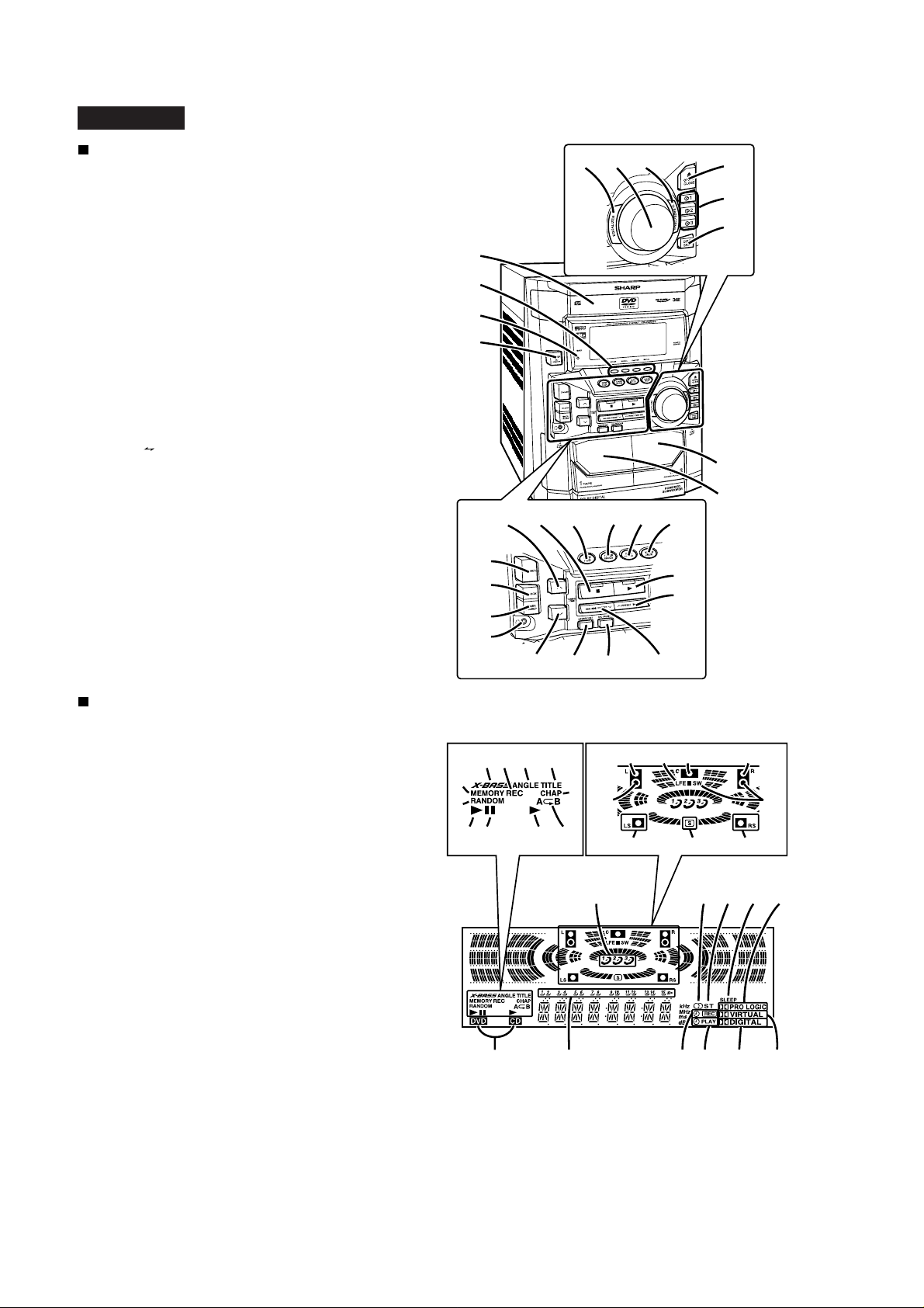
CD-DVD500
CD-DVD500
Front panel
01.
Disc Tray
02.
Surround Effect Buttons
3.
Timer Set Indicator
4.
Power On/Stand-by Button
5.
Tape 2 Cassette Compartment
6.
Tape 1 Cassette Compartment
7.
Equaliser Mode Select Button
8.
Volume Control
9.
Extra Bass/Demo Mode Button
10.
Disc Tray Open/Close Button
11.
Disc Number Select Buttons
12.
Disc Skip Button
13.
Tuning and Time Up Button
14.
DVD/CD/Tape Stop Button (with Indicator)
15.
DVD/CD Button
16.
Tuner (Band) Button
17.
Tape (1 2) Button
18.
Video/Auxiliary Button
19.
Dimmer Button
20.
Clock Button
21.
Timer/Sleep Button
22.
Headphone Socket
23.
DVD/CD/Tape Play Button (with Indicator)
24.
DVD Chapter skip, DVD/CD/Tape 2 Fast Forward
or Tuner Preset Up Button
25.
Tuning and Time Down Button
26.
Memory/Set Button
27.
Tape 2 Record Pause Button
28.
DVD Chapter skip, DVD/CD Fast Reverse,
Tape 2 Rewind or Tuner Preset Down Button
NAMES OF PARTS
1
2
3
4
19
20
21
22
25 26 27 28
78
9
10
11
12
5
6
181716151413
23
24
Display
1.
Extra Bass Indicator
2.
Tape 2 Record Indicator
3.
DVD Angle Indicator
4.
DVD Title Indicator
5.
Memory Indicator
6.
CD Random Play Indicator
7.
DVD Chapter Indicator
8.
DVD/CD Play Indicator
9.
DVD/CD Pause Indicator
10.
Tape Play Indicator
11.
DVD/CD Repeat Indicator
12.
Left Front Speaker Indicator
13.
Low Frequency Effect Indicator
14.
Centre Speaker Indicator
15.
Right Front Speaker Indicator
16.
Subwoofer Indicators
17.
Left Surround Speaker Indicator
18.
Surround Indicator
19.
Right Surround Speaker Indicator
20.
Disc Number Indicators
21.
FM Stereo Receiving Indicator
22.
FM Stereo Mode Indicator
23.
Sleep Indicator
24.
Dolby Pro Logic Indicator
25.
Disc Types Indicators
26.
CD Music Schedule Indicators
27.
Timer Recording Indicator
28.
Timer Play Indicator
29.
Dolby Digital Indicator
30.
Dolby Virtual Indicator
32 4
5
6
819 1011
25
12 13 14
7
16 16
17 18 19
20
26
21 22 23 24
2728 29
15
30
– 3 –
Page 4
CD-DVD500
CD-DVD500
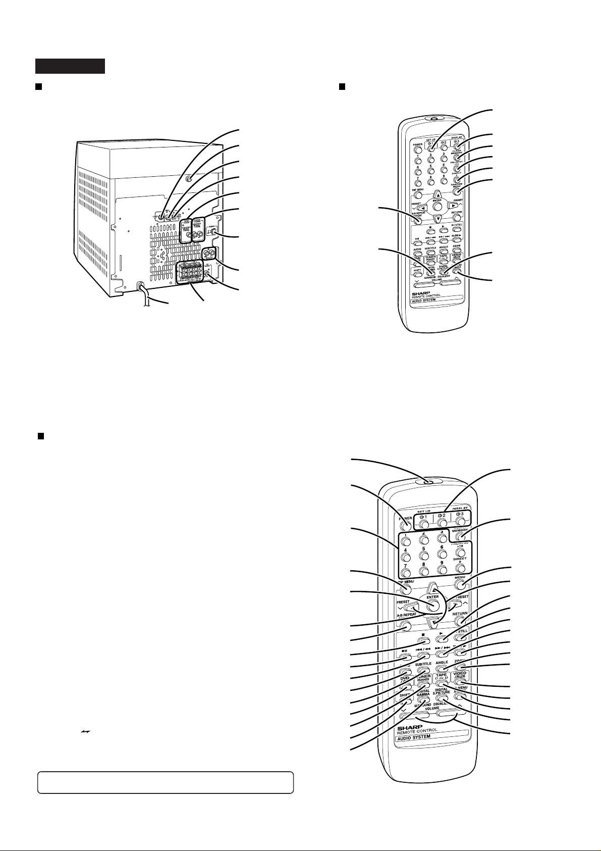
Remote control with shift buttonRear panel
3
1
2
3
4
5
6
7
8
9
10
1.
S-video Output Socket
2.
Transport Screw
3.
Video Output Socket
4.
Audio Digital Output Socket
5.
Centre Speaker Socket
6.
Surround Speaker Sockets
7.
FM/AM Loop Aerial Socket
8.
Video/Auxiliary (Audio Signal) Input Sockets
9.
Subwoofer Pre Output Socket
10.
AC Power Lead
11.
Speaker Terminals
11
Remote control
1.
Remote Control Transmitter
2.
Power Button
3.
Direct Buttons
4.
DVD Top Menu Button
5.
Enter Button
6.
Menu Select or Tuner Preset Buttons
7.
DVD/CD Repeat Button
8.
DVD/CD/Tape Stop Button
9.
Tape 2 Record Pause Button
10.
DVD Chapter Skip or DVD/CD/Tape Fast Reverse Button
11.
DVD Audio Button
12.
DVD Subtitle Button
13.
DVD/CD Button
14.
Tuner (Band) Button
15.
Shift Button
16.
Surround Button
17.
Disc Number Select Buttons
18.
DVD/CD Memory Button
19.
DVD Menu Button
20.
Menu Select Buttons
21.
Return Button
22.
DVD/CD/Tape Play Button
23.
DVD/CD Pause Button
24.
DVD Chapter Skip or DVD/CD/Tape Fast Forward Button
25.
DVD Slow Button
26.
DVD Angle Button
27.
DVD Zoom Button
28.
Video/Auxiliary Button
29.
Tape (1 2) Button
30.
Extra Bass Button
31.
Equaliser Button
32.
Volume Up or Down Buttons
Buttons with “✱” mark in the illustration can be operated with the remote control only.
Other buttons can be operated on the main unit and the remote control.
✱
✱
✱
✱
✱
✱
✱
✱
✱
✱
10
11
12
13
14
15
16
4
5
6
7
8
1
2
9
10
1.
DVD/CD A-B Repeat Button
2.
DVD Digital Gamma Button
3.
DVD Setup Button
4.
Display Button
5.
Clear Button
6.
PAL/NTSC Button
7.
Direct Button
8.
CD Random Button
9.
DVD Digital Super Picture Button
10.
Speaker Menu Button
1
17
2
18
✱
3
19
4
5
20
21
✱
✱
✱
22
23
6
7
8
9
24
25
26
27
✱
✱
✱
✱
28
29
30
31
32
– 4 –
Page 5
CD-DVD500
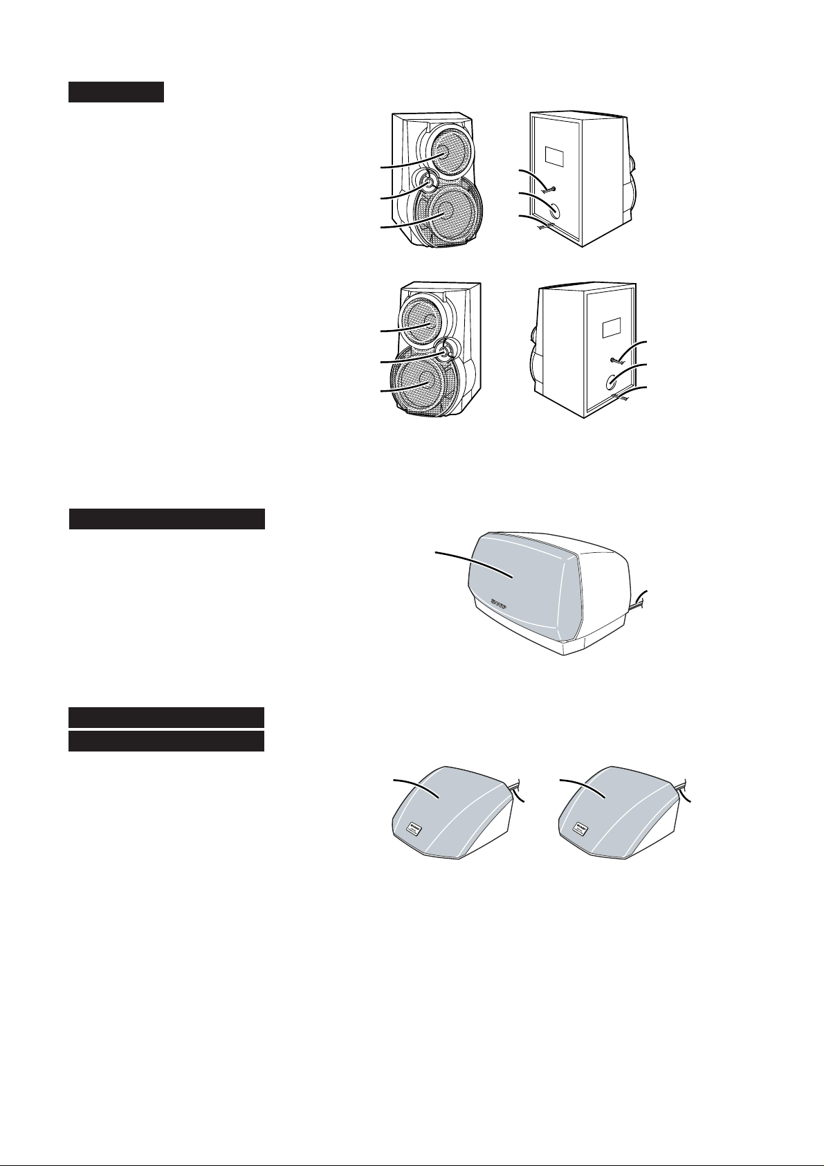
CP-DVD500
01.
Woofer
02.
Tweeter
03.
Subwoofer
04.
Speaker Wire for SUBWOOFER Terminals
05.
Bass Reflex Duct
06.
Speaker Wire for MAIN Terminals
Front speaker
(left)
1
2
3
Front speaker
(right)
1
2
3
4
5
6
4
5
6
GBOXS0064AWM4
01.
Full-Range Speaker
02.
Speaker Wire
GBOXS2008AWM4
GBOXS4008AWM4
01.
Full-Range Speaker
02.
Speaker Wire
Centre speaker
1
Surround speaker
(left)
1
Surround speaker
(right)
1
2
2
2
– 5 –
Page 6
CD-DVD500
OPERATION MANUAL
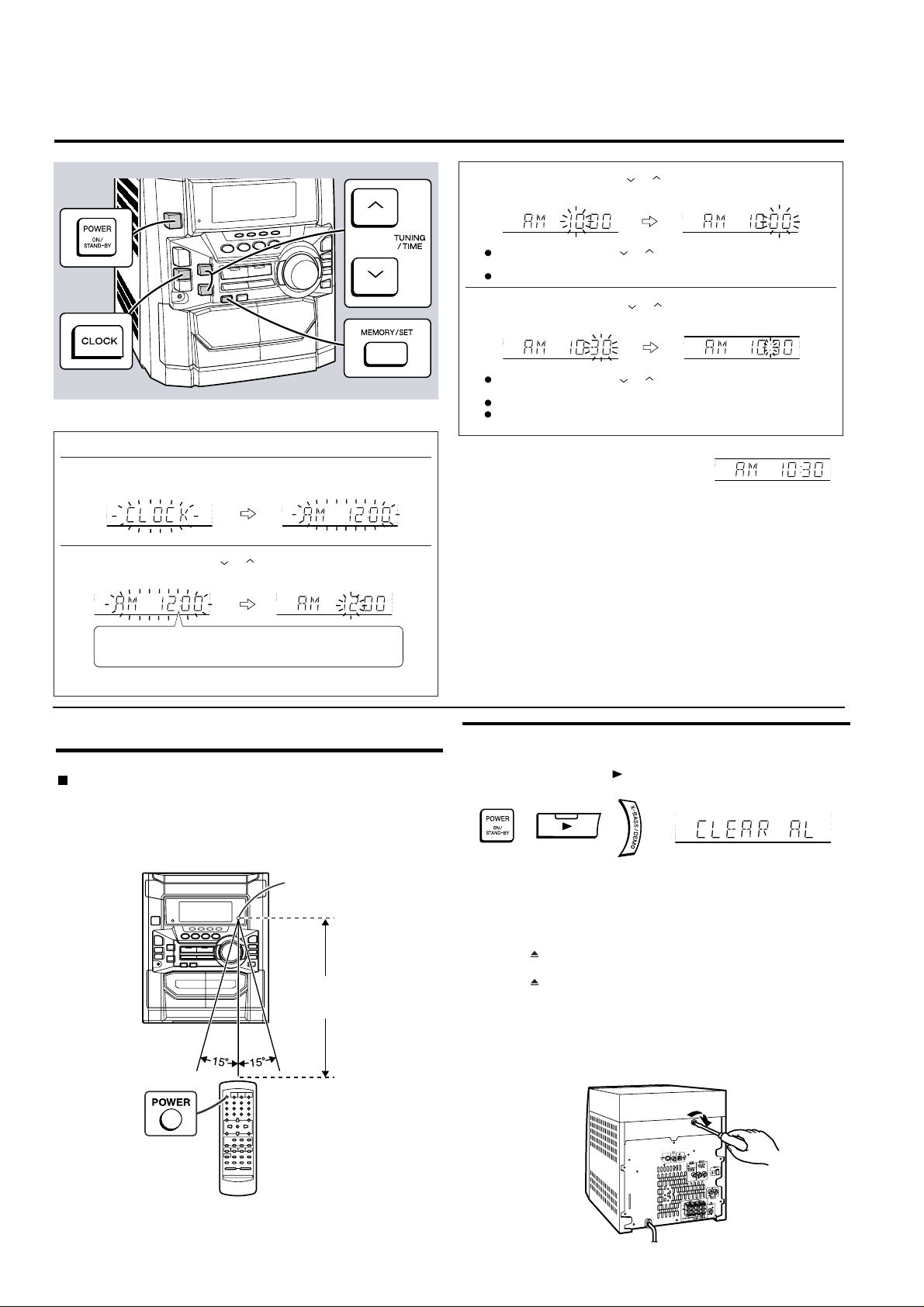
Setting the Clock
In this example, the clock is set for the 12-hour (AM 12:00) display.
1
Press the POWER button to turn the power on.
2
Press the CLOCK button and within 5 seconds, press the
MEMORY/SET button.
3
Press the TUNING/TIME ( or ) button to select the 12-hour or
24-hour display and then press the MEMORY/SET button.
“AM 12:00”→ The12-hour display will appear. (AM 12:00 - PM 11:59)
“AM 0:00” → The12-hour display will appear. (AM 0:00 - PM 11:59)
“0:00” → The 24-hour display will appear. (0:00 - 23:59)
Note that this can only be set when the unit is first installed or it has been reset.
4
Press the TUNING/TIME ( or ) button to adjust the hour and
then press the MEMORY/SET button.
Press the
TUNING/TIME ( or )
hour
When the 12-hour display is selected, “AM” will change automatically to “PM”.
5
Press the TUNING/TIME ( or ) button to adjust the minutes
and then press the MEMORY/SET button.
Press the
TUNING/TIME ( or )
minute. Hold it down to change the time in 5-minute intervals.
The hour will not advance even if minutes advance from “59” to “00”.
The clock begins counting from “0” seconds. (Seconds are not displayed.)
The time display will disappear after a few seconds.
To confirm the time display:
Press the CLOCK button.
The time display will appear for about 5 seconds.
Note:
The “CLOCK” or time will flash at the push of the CLOCK button when the AC power
supply is restored after a power failure or unplugging the unit.
Readjust the clock as follows.
To readjust the clock:
Perform “Setting the Clock” from the beginning.
If the time display is flashing, step 3 (for selecting the 12-hour or 24-hour display) will
be skipped.
To change the 12-hour or 24-hour display:
1. Clear all the programmed contents.
[Refer to “Clearing all the memory (reset)”.]
2. Perform “Setting the Clock” from the beginning.
button once to advance the time by 1
button once to advance the time by 1
Remote Control
Test of the remote control
Face the remote control directly to the remote sensor on the unit.
The remote control can be used within the range shown below:
Press the POWER button. Does the power turn on? Now, you can enjoy your system.
Remote sensor
0.2 m - 6 m
(8" - 20')
■
Clearing all the memory (reset)
1
. Press the POWER button to enter the power stand-by mode.
2
.Whilst pressing down the button and X-BASS/DEMO button, press the
POWER button until “CLEAR AL” appears.
Caution:
This operation will erase all data stored in memory including clock, timer settings,
tuner preset.
■
Before transporting the unit
1.
Press the POWER button to turn the power on.
2.
Press the DVD/CD button.
3.
Press the OPEN/CLOSE button to open the disc tray.
Remove all discs from the unit.
4.
Press the OPEN/CLOSE button to close the disc tray.
Make sure that “NO DISC” is displayed.
5.
Press the POWER button to enter the stand-by mode, “GOOD-BYE” is displayed.
6.
When “GOOD-BYE” disappears, unplug the AC power lead from the AC
socket.
7.
Insert the transport screw into the back of the unit and tighten it with a flatblade screwdriver.
– 6 –
Page 7
Troubleshooting Chart
CD-DVD500
Many potential “problems” can be resolved by the owner without calling a service technician. If something is wrong with this product, check the following before calling your
authorised SHARP dealer or service centre.
■
General
Symptom
● The clock is not accurate.
●
When a button is pressed, the unit
does not respond.
● No sound is heard.
● The balance between the left and
right channels is bad.
● Hum or excessive noise.
● No sound is heard, or the sound
is too low, from the centre or surround speakers.
● The timer indicator is flashing.
● Did a power failure occur?
● Set this unit to the power stand-by mode
● If the unit still malfunctions, reset it.
● Is the volume level set to “0”?
● Are the headphones connected?
● Are the speaker wires disconnected?
● Are the front and surround speakers
● If an external unit is connected, are the
● Is the speaker lead plugged in i ncor-
● Does the speaker lead run past other
● Are the plugs or terminals dirty?
● Is the “speaker size” item set to “NO” in
● Is the volume too low?
● Is the speaker wire shorted?
● Was the unit used at high volume for
Possible cause
Reset the clock.
and then turn it back on.
connected to the wrong channels?
left and right channels connected im-
properly?
rectly?
electronic equipment?
the “setup” operation?
many hours?
■
DVD/CD player
Symptom
● No image from the DVD video
appears on the screen of a connected device.
● Playback does not start.
● Playback stops in the middle or is
not performed properly.
● Playback sounds are skipped, or
stopped in the middle of a track.
Possible cause
● Make sure the channel of the connected
TV is set to VIDEO or AV.
● Make sure video cables are connected
correctly.
● Is the disc loaded upside down?
● Does the disc dissatisfy the standards?
● Is the disc distorted or scratched?
● Is the unit located near excessive vibra-
tions?
● Is the disc very dirty?
● Has condensation formed inside the
unit?
Troubleshooting Chart
■
Tuner
Symptom
● Radio makes constant unusual
noise or static.
■
Cassette deck
Symptom
● Cannot record.
● Cannot record tracks with proper
sound quality.
● Cannot erase completely.
● Sound skipping.
● Cannot hear treble.
● Sound fluctuation.
● Cannot remove the tape.
■
Remote control
Symptom
● The remote control does not op-
erate.
● Is the unit placed near the TV or com-
● Is the FM/AM loop aerial placed improp-
● Is the erase-protection tab removed?
● Is it a normal tape?
● Is there any slack?
● Is the tape stretched?
● Are the capstans, pinch rollers, or heads
● If a power failure occurs during playback,
● Is the AC power lead of the unit un-
● Is the battery polarity wrong?
● Are the batteries dead?
● Is the distance or angle incorrect?
● Does the remote control sensor receive
Possible cause
puter?
erly?
Move the AC power lead away from the
aerial if located near.
Possible cause
(You cannot record on a metal or CrO
tape.)
dirty?
the heads remain engaged with the tape.
Do not open the compartment forcibly.
Wait until electricity resumes.
Possible cause
plugged?
strong light?
■
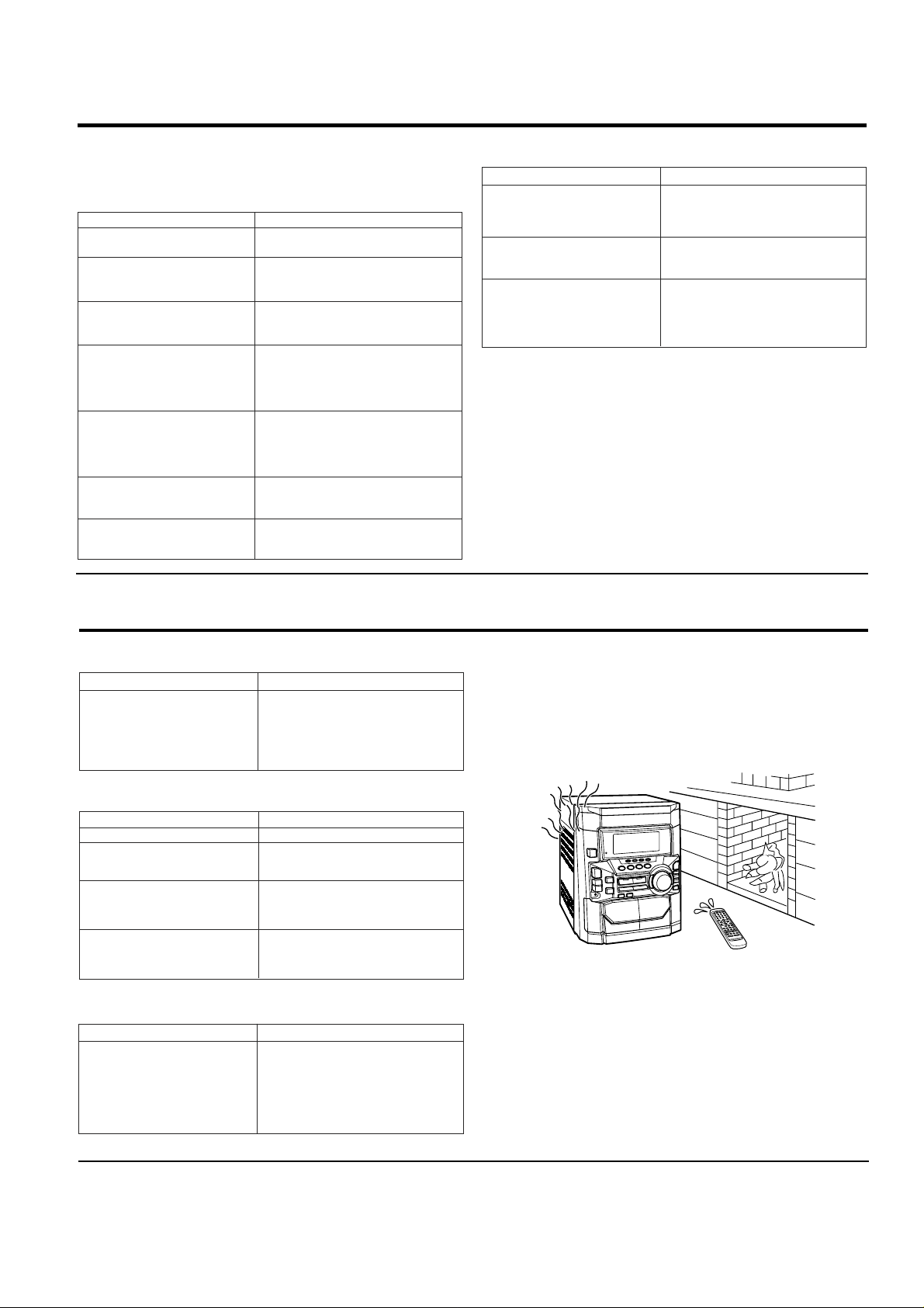
Condensation
Sudden temperature changes, storage or operation in an extremely humid environment may cause condensation inside the cabinet (DVD/CD pickup, tape heads, etc.)
or on the transmitter on the remote control.
Condensation can cause the unit to malfunction.
If this happens, leave the power on with no disc (or cassette) in the unit until normal
playback is possible (about 1 hour). Wipe off any condensation on the transmitter with
a soft cloth before operating the unit.
2
■ If trouble occurs
When this product is subjected to strong external interference (mechanical shock, excessive static electricity, abnormal supply voltage due to lightning, etc.) or if it is operated incorrectly, it may malfunction.
If such a problem occurs, do the following:
1. Set the unit to the stand-by mode and turn the power on again.
2. If the unit is not restored in the previous operation, unplug and plug in the
unit, and then turn the power on.
Note:
If neither operation above restores the unit, clear all the memory by resetting it.
– 7 –
Page 8
CD-DVD500
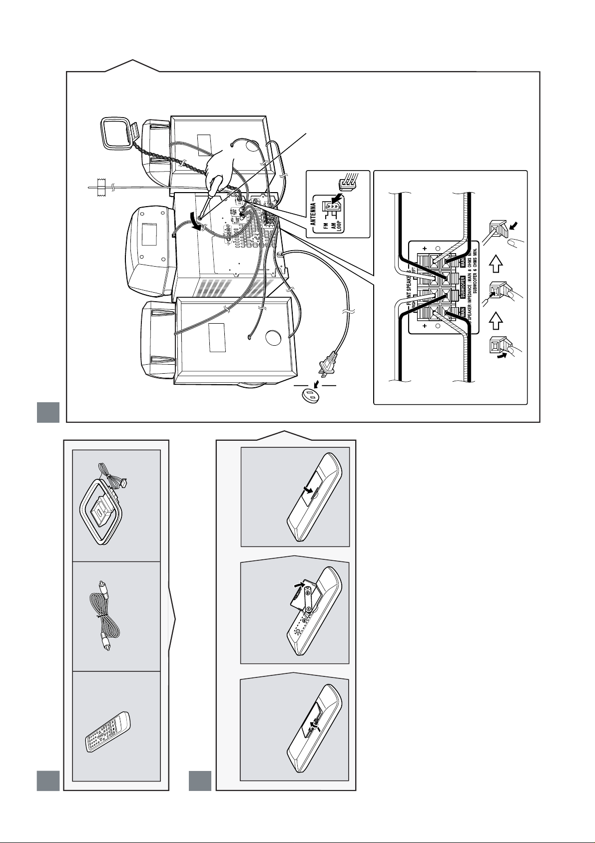
Accessories
Accesorios
FM/AM loop antenna 1
Antena de cuadro de FM/AM 1
Remote control 1
Controlador remoto 1
1
3
Battery Installation of the Remote Control
Instalación de las pilas del controlador remoto
Use 2 “AA” size batteries (UM/SUM-3, R6, HP-7 or similar). Batteries are not included.
Use dos pilas del tamaño “AA” (UM/SUM-3, R6, HP-7 o equivalentes). Las pilas no están incluidas.
Remove the
Insert the batteries
Replace the cover.
battery cover.
as shown.
Extraiga la cubierta Inserte las pilas Vuelva a colocar la
de las pilas. como se muestra. cubierta.
2
Video cable 1
Cable de vídeo 1
System Connections
Conexiones del sistema
AC outlet
(AC 120 V, 60 Hz)
A un tomacorriente de
CA (120 V de CA, 60 Hz)
Front speaker (Right)
Altavoz delantero (Derecho)
Front speaker (Left)
Altavoz delantero
(Izquierdo)
FM antenna
Antena de FM
AM loop antenna
Antena de cuadro de AM
Blue
Azul
Red
Rojo
Black
Negro
Black
Negro
Blue
Azul
Red
Rojo
Black
Negro
Black
Negro
Surround speaker (Right)
Altavoz surround (Derecho)
Surround
speaker
(Left)
Altavoz
surround
(Izquierdo)
Center speaker
Altavoz central
Right
Derecho
Left
Izquierdo
Before turning the power on, be
sure to remove this transport
screw on the back of the unit
using a flat-blade screwdriver
or a coin.
This screw is required when
transporting the unit again.
Please keep it.
Antes de conectar la alimentación,
asegúrese de extraer este tornillo
para el transporte de la parte pos-
terior del aparato empleando un
destornillador de punta plana o
una moneda.
Este tornillo es necesario cuando
el aparato se transporta de nuevo.
Gurádelo.
– 8 –
Page 9
CD-DVD500
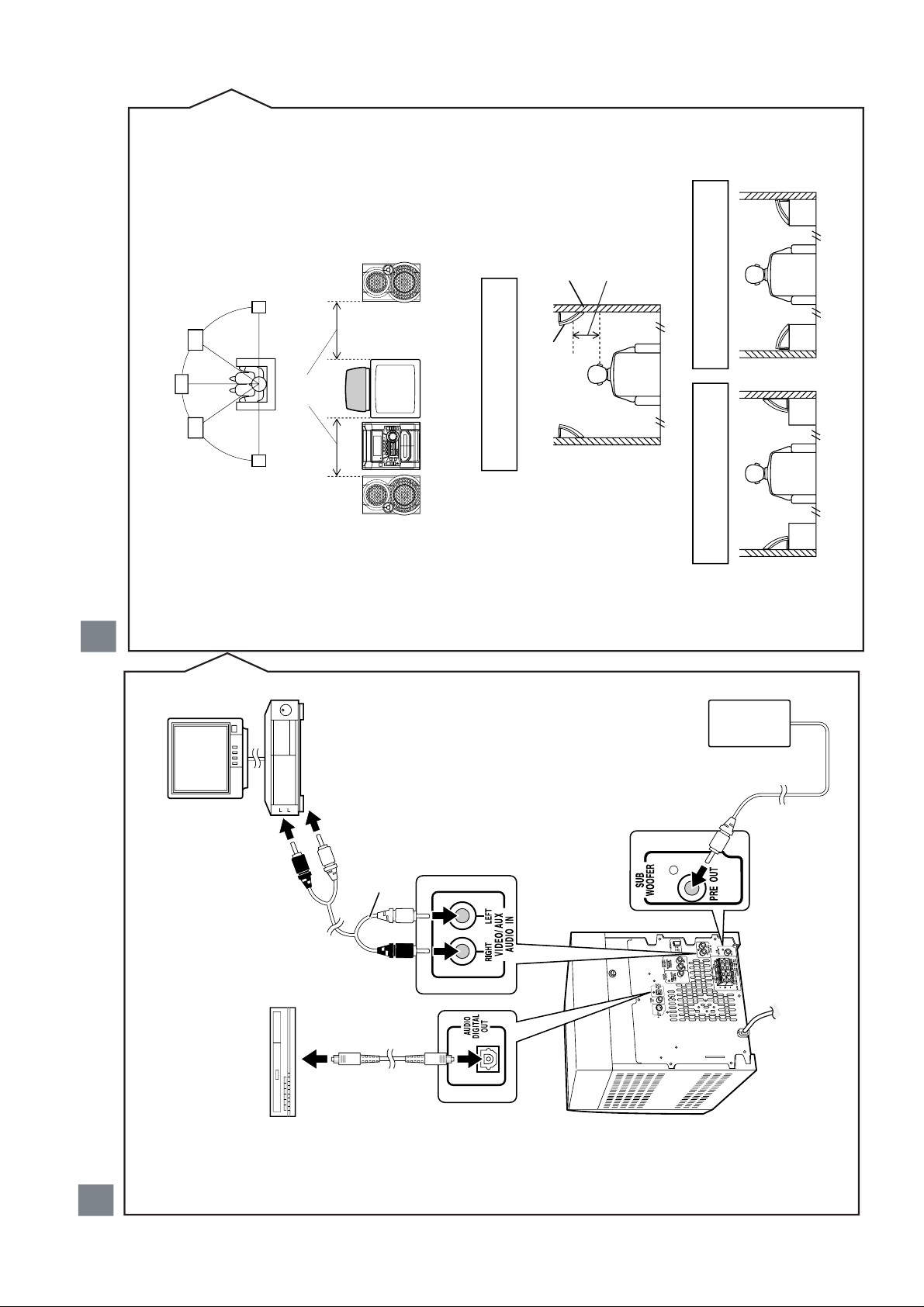
External Unit Connections
Conexiones de unidades externas
RCA cord
(not supplied)
Cable RCA
(no suministrado)
To the line output jacks
A las tomas de salida de línea
VCR
Videograbadora
TV
TV
MD recorder, Dolby Digital (5.1 ch)/
DTS processor or amplifier
Grabadora de MD,Procesador o
amplificador Dolby Digital (5.1 ch)/DTS
Digital cord
(not supplied)
Cable digital
(no suministrado)
Speaker with a
built-in amplifier
Altavoz con amplificador
incorporado
Front left
Delantero izquierdo
Center
Central
Front right
Delantero derecho
Surround left
Surround izquierdo
Surround right
Surround derecho
Same distance
Misma distancia
Front left
Delantero izquierdo
Center
Central
Front right
Delantero derecho
Example: When installed on the wall
Ejemplo: Cuando se instalan en la pared
Surround speaker
Altavoz surround
Wall
Pared
23-5/8" - 35-7/16"
(60 - 90 cm)
60 - 90 cm
Example: When installed vertically
Ejemplo: Cuando se instalan verticalmente
Example: When installed horizontally
Ejemplo: Cuando se instalan horizontalmente
Placing the Speakers
Situación de los altavoces
– 9 –
Page 10
CD-DVD500
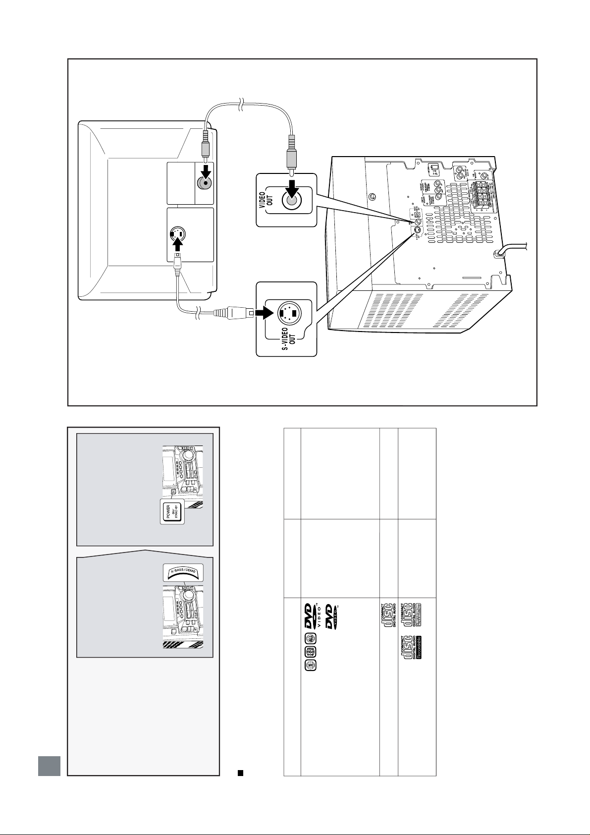
Turning on Your System
Conexión de la alimentación de su sistema
The first time the unit is plugged
in, the unit will enter the demon-
stration mode. Y ou will see words
scroll.
Cuando se enchufe por primera vez
el aparato, se establecerá en el
modo de demostración. Verá un
desplazamiento de palabras.
Press the
X-BASS/DEMO
button to cancel
the demonstration
mode.
Pulse el botón
X-BASS/DEMO para
cancelar el modo de
demostración.
Press the POWER
button to turn the
power on.
Pulse el botón POWER
para conectar la
alimentación.
12
Prepare the disc you want to play
Prepare el disco que desee reproducir
Supported disc types
Tipos de discos soportados
Disc type
Tipo de disco
DVD Video Disc
Region Numbers:
NTSC system
DVD discs that conform to the region numbers
noted above
Disco DVD vídeo
Números de región:
Sistema NTSC
Discos DVD que conforman los números de región
mencionados arriba
Audio CD
CD de audio
CD-R/CD-RW
Discs recorded in audio format
CD-R/CD-RW
Discos grabados en el formato de audio
Disc contents
Contenido del disco
Audio and video (movies)
Audio y vídeo (películas)
Audio
Audio
Audio
Audio
Disc size
Tamaño del disco
5" (12 cm) / 3" (8 cm)
12 cm/8 cm
5" (12 cm) / 3" (8 cm) (single)
12 cm/8 cm (sencillo)
5" (12 cm) / 3" (8 cm)
12 cm/8 cm
Video cable
(Supplied)
Cable de vídeo
(Suministrado)
S-video cable
(commercially available)
Cable de S-vídeo
(disponible
comercialmente)
S-VIDEO INPUT
VIDEO IN
To TV with external terminals
Al televisor con terminales externos
Connecting a TV with External Terminals
Conexión de un televisor con terminales externos
– 10 –
Page 11
CD-DVD500
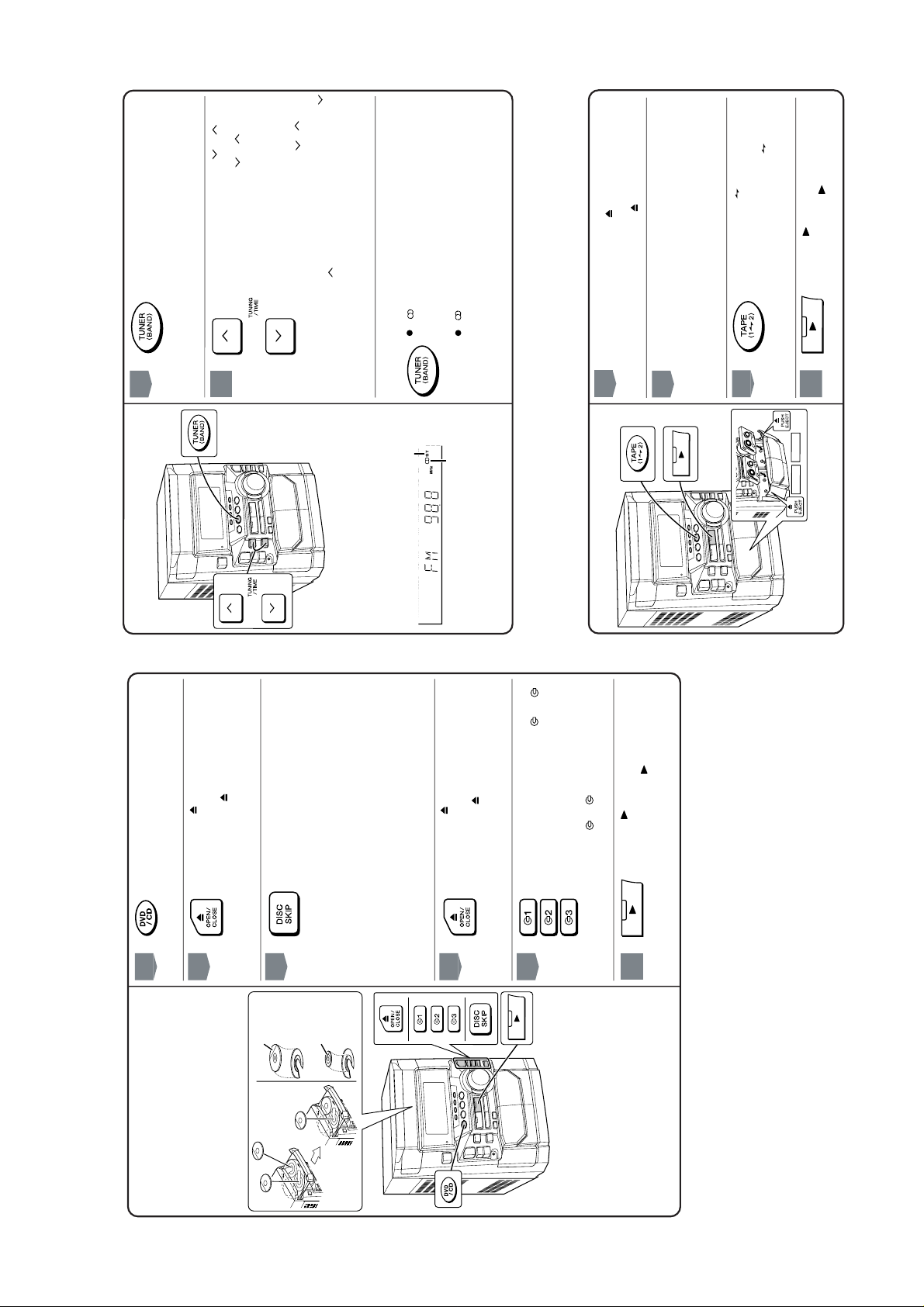
Playing a DVD/CD (DVDs/CDs)
Reproducción de un disco DVD/CD (discos DVD/CD)
1
Press the DVD/CD button.
Pulse el botón DVD/CD.
2
Press the OPEN/CLOSE button to
open the disc tray.
Pulse el botón OPEN/CLOSE para abrir
la bandeja de discos.
3
Place the DVD(s) or CD(s) on the disc
tray, label side up.
When loading a third disc, press the
DISC SKIP button to turn the disc tray,
then place the CD in the open position.
Coloque el disco DVD o CD en la bandeja
de discos, con el lado de la etiqueta hacia
arriba.
Cuando ponga un tercer disco, pulse el
botón DISC SKIP para girar la bandeja de
discos, y coloque el disco compacto en la
posición abierta.
4
Press the OPEN/CLOSE button to
close the disc tray.
Pulse el botón OPEN/CLOSE para cerrar
la bandeja de discos.
5
To select the DVD or CD you want to lis-
ten to first, press one of the 1 - 3
buttons.
Para seleccionar el disco DVD o CD que
desee escuchar primero, pulse uno de los
botones 1 - 3.
6
Press the button to start playback.
Pulse el botón para iniciar la
reproducción.
5” (12 cm)
12 cm
3” (8 cm)
8 cm
Listening to a Cassette Tape (TAPE 1 or TAPE 2)
Audición de una cinta de cassette (TAPE 1 o TAPE 2)
Listening to the Radio
Audición de la radio
TAPE 1
TAPE 2
FM stereo mode indicator
Indicador del modo de FM
en estéreo
FM stereo receiving indicator
Indicador de recepción de FM
en estéreo
1
Press the TUNER (BAND) button repeat-
edly to select the desired frequency
band (FM or AM).
Pulse repetidamente el botón TUNER
(BAND) para seleccionar la banda de
frecuencia deseada (FM o AM).
2
Press the TUNING/TIME ( or ) but-
ton to tune in to the desired station.
When the TUNING/TIME ( or ) button
is pressed for more than 0.5 seconds,
scanning will start automatically and the
tuner will stop at the first receivable
broadcast station.
Pulse el botón TUNING/TIME ( o ) para
sintonizar la emisora deseada.
Cuando se pulse el botón
TUNING/TIME (
o ) durante más de 0,5 segundos, la
exploración se iniciará automáticamente y
el sintonizador se parará en la primera
emisora difusora que pueda recibirse.
To receive an FM stereo transmission:
Press the TUNER (BAND) button to display “ST”.
“ ” will appear when an FM broadcast is in ste-
reo.
Para recibir una transmisión de FM en estéreo:
Pulse el botón TUNER (BAND) para visualizar “ST”.
“ ” aparecerá cuando una difusión de FM sea en
estéreo.
1
Open the cassette door by pushing the
area marked “ PUSH EJECT”.
Abra la puerta del cassette pulsando la
parte marcada “ PUSH EJECT”.
2
Load the cassette into the TAPE 1 or
TAPE 2 cassette compartment with the
side to be played facing toward you.
Cargue el cassette en el compartimiento
de cassette de TAPE 1 o de TAPE 2 con la
cara a reproducirse encarada hacia usted.
3
Press the TAPE (1 2) button to select
the cassette you want to listen to.
Pulse el botón TAPE (1 2) para
seleccìonar el cassette que desee
escuchar.
4
Press the button to start playback.
Pulse el botón para iniciar la
reproducción.
– 11 –
Page 12
(B1) x 4
ø3 x 10mm
(B1) x 2
ø3 x 10mm
Rear
Panel
(B1) x 2
ø3 x 10mm
Side Panel
(Right)
Side Panel
(Left)
(A1) x 2
ø3 x 12mm
(A1) x 2
ø3 x 12mm
Top Cabinet
CD-DVD500
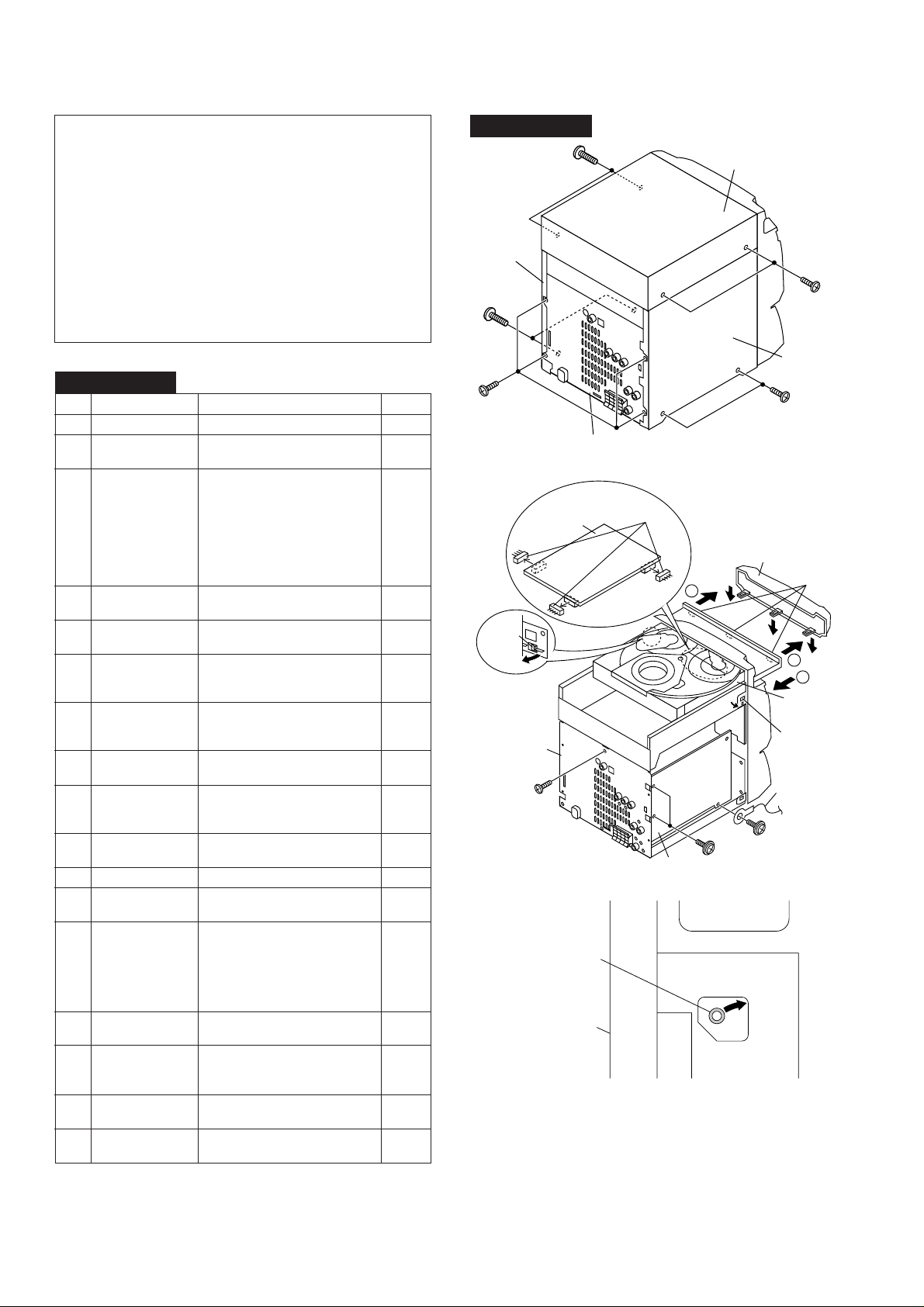
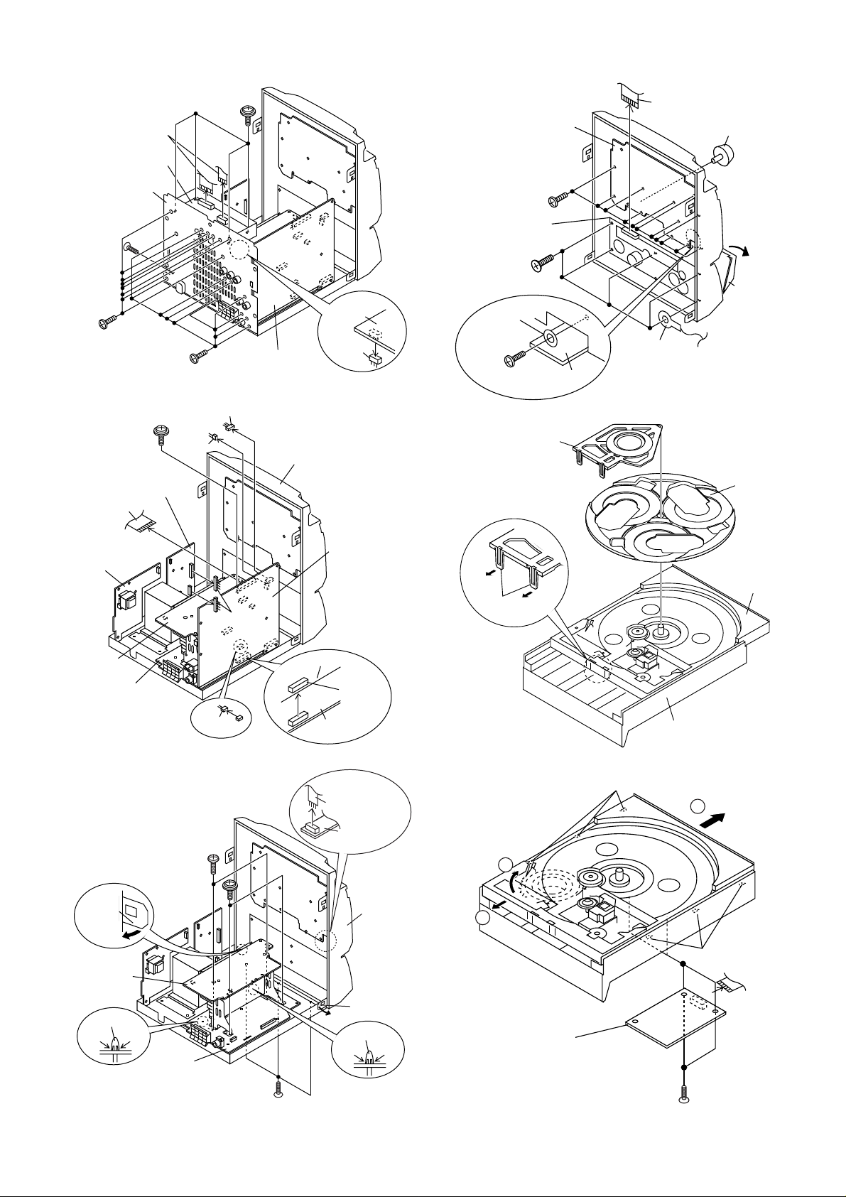
DISASSEMBLY
Caution on Disassembly
Follow the below-mentioned notes when disassembling
the unit and reassembling it, to keep it safe and ensure
excellent performance:
1. Take cassette tape and compact disc out of the unit.
2. Be sure to remove the power supply plug from the wall
outlet before starting to disassemble the unit.
3. Take off nylon bands or wire holders where they need to
be removed when disassembling the unit. After servicing
the unit, be sure to rearrange the leads where they were
before disassembling.
4. Take sufficient care on static electricity of integrated
circuits and other circuits when servicing.
CD-DVD500
STEP
10 Tape Mechanism 1. Open the cassette holder. 13-4
11
12 Turntable 1. Hook....................... (M1) x2 13-5
13 Disc Tray 1.
REMOVAL
1 Top Cabinet 1. Screw ..................... (A1) x4 12-1
2 Side Panel 1. Screw ..................... (B1) x8 12-1
(Left/Right)
3 DVD Player 1. Turn on the power supply, 12-2
Unit/DVD Tray open the disc tray, take out
Cover
4 Dolby PWB 1. Screw ................... (D1) x12 13-1
5 Rear Panel with 1. Screw ....................(E1) x13
Fan Motor 2. Socket ..................... (E2) x1 13-1
6 Main PWB 1. Screw..................... (F1) x2
7 AMP. A/AMP. B 1. Screw ..................... (G1) x4 13-3
PWB with Heat Sink
8 Front Panel 1. Screw ..................... (H1) x3 13-3
9 Display PWB 1. Knob ........................ (J1) x1 13-4
Headphones PWB
(Note 1)
2. Screw ..................... (C1) x1
3. Hook....................... (C2) x3
4. Hook....................... (C3) x2
5. Socket .................... (C4) x3 12-2
2. Flat Cable .............. (D2) x2
2. Flat Cable .............. (F2) x1 13-2
3. Socket .................... (F3) x6
2. Flat Wire................. (G2) x1
3. PWB Holder ........... (G3) x2
2.Hook........................ (H2) x2
2. Screw .................... (J2) x11
3. Flat Cable ............... (J3) x1
2. Screw...................... (K1) x5
1. Screw ..................... (L1) x1 13-4
2. Cover ..................... (M2) x1
2.
14 DVD Servo PWB 1. Screw ..................... (P1) x2 13-6
(Note 2) 2. Flat Cable .............. (P2) x1
15 Joint PWB 1. Screw ..................... (Q1) x2 14-1
16 DVD Mechanism 1. Hook ....................... (R1) x2 14-2
17 DVD Loading 1. Hook....................... (S1) x6 14-3
Motor PWB
Note 1: How to open the changer manually. (Fig. 12-3)
1. In this state, turn fully the lock lever in the arrow direction through
the hole on the loading chassis bottom.
2. After that, push forward the slide Chissis.
2. Hook....................... (Q2) x3
3. Socket .................... (Q3) x2
2. Hook....................... (R2) x3
PROCEDURE
the DVD tray cover, and close.
Turn fully the lock lever in the
arrow direction
Push the slide chissis backward to
engage the claw with the groove
and remove it in the direction
of the arrow. ...............
.
(N1) x6
FIGURE
12-2,13-1
12-2,13-2
12-3
13-6
CD-DVD500
Figure 12-1
(C4) x 3
Main PWB
1
DVD Tray Cover
Lug Wire
(F1) x 1
(E1) x 2
ø3 x 10mm
ø3 x 10mm
(C2) x 3
1
2
DVD Player
Unit
(C3) x 1
(C3) x 1
Pull
(C1) x 1
ø3 x 10mm
DVD Servo
PWB
Rear
Panel
Figure 12-2
Lock Lever
DVD Player Unit
(Bottom View)
Note 2:
1. After removing the connector for the optical pickup from the
connector, wrap the conductive aluminium foil around the front end
of the connector so as to protect the optical pickup from electrostatic damage.
Note 3:
1. Be careful not to break the claw of the DVD mechanism.
2. When fining back the cam gear assembly, let it lock by front
movement.
Figure 12-3
– 12 –
Page 13
DVD Player Unit
Slide
Chassis
Turntable
(M2) x 1
(M1) x 2
Rear
(J3) x 1
(J2) x 11
ø3 x 10mm
(K1) x 5
ø3 x 10mm
(J1) x 1
Display PWB
Headphones
PWB
Open
Cassette
Holder
Tape
Mechanism
(L1) x 1
ø3 x 10mm
Lug Wire
Washer
Panel
(E1) x 1
ø3 x 10mm
(D1) x 8
ø3 x 10mm
(F1) x 1
ø3 x 10mm
Power PWB
(F2) x 1
(D2) x 2
Dolby
PWB
(E1) x 10
ø3 x 10mm
(F3) x 1
(D1) x 4
ø3 x 10mm
Main PWB
Figure 13-1
(F3) x 1
Front
Panel
Amp. B
PWB
(E2) x 1
CD-DVD500
Figure 13-4
Transformer
PWB
Amp. B
PWB
(H2) x 1
Amp. A
PWB
(G1) x 2
ø3 x 6mm
(G1) x 2
ø3 x 10mm
(F3) x 2
(F3) x 1
Figure 13-2
Main PWB
Main PWB
Amp. A
PWB
(G2) x 1
Headphones
PWB
(F3) x 1
Front
Panel
Figure 13-5
(N1) x 3
3
2
1
Amp. B
PWB
(G3)x1
(N1) x 3
(H2) x 1
PushPush
Amp. A
PWB
(H1) x 3
ø3 x 8mm
Figure 13-3
(G3)x1
DVD Servo
PushPush
PWB
(P1) x 2
ø3 x 8mm
Figure 13-6
– 13 –
(P2) x 1
Page 14
CD-DVD500
Screwdriver
Driver should
be pried away
from Speaker Box.
(A1) x 1
Speaker Box
Joint PWB
(Q3) x 2
(Q1) x 2
ø3 x 8mm
DVD
Mechanism
(R1) x 1
(Q2) x 3
Figure 14-1
(R1) x 1
Slide
Chassis
(R2) x 3
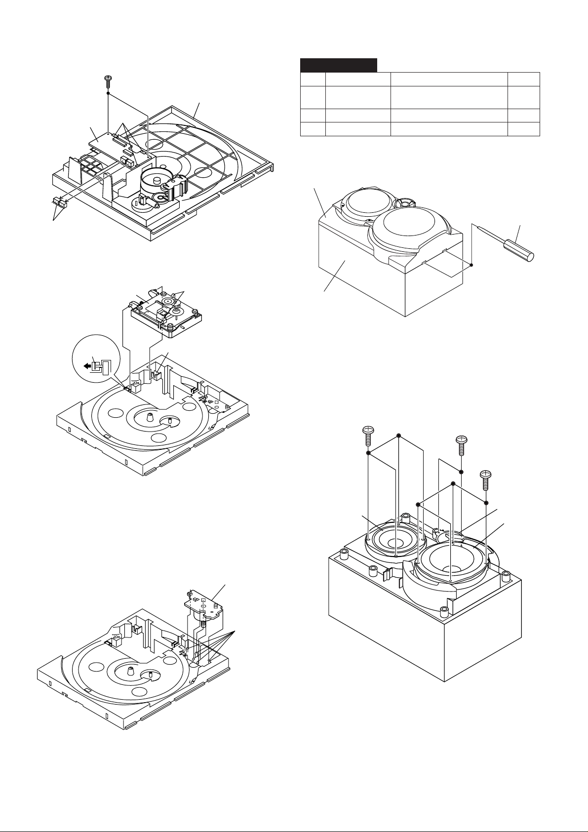
CP-DVD500
STEP
REMOVAL PROCEDURE
1 Subwoofer 1. Front Panel ............ (A1) x1 14-4
2. Screw ..................... (A2) x4 14-5
2 Woofer 1. Screw ..................... (B1) x4 14-5
3 Tweeter 1. Screw ..................... (C1) x2 14-5
Figure 14-4
FIGURE
Figure 14-2
DVD Loading
Motor PWB
(S1) x 6
(A2) x 4
ø 4 x 16mm
Subwoofer
(C1) x 2
ø 3 x 10mm
(B1) x 4
ø 4 x 16mm
Tweeter
Woofer
Figure 14-5
Figure 14-3
– 14 –
Page 15
REMOVING AND REINSTALLING THE MAIN PARTS
TAPE MECHANISM SECTION
Perform steps 1 to 8 and 10 of the disassembly method to
remove the tape mechanism.
How to remove the record/playback and erase
heads (TAPE 2) (See Fig. 15-1)
1. When you remove the screws (A1) x 2 pcs., the recording/
playback head and three-dimensional head of the erasing
head can be removed.
How to remove the playback head (TAPE 1)
(See Fig. 15-2)
1. When you remove the screws (B1) x 2 pcs., the playback
head.
How to remove the pinch roller (TAPE 1/2)
(See Fig. 15-3)
1. Carefully bend the pinch roller pawl in the direction of the
arrow <A>, and remove the pinch roller (C1) x 1 pc., in the
direction of the arrow <B>.
Note:
When installing the pinch roller, pay attention to the spring
mounting position.
Erase Head
(A1)x2
Ø2 x 9mm
TAPE 1
TAPE 2
Figure 15-1
CD-DVD500
Clutch Ass'y
Record/Playback
Head
Clutch Ass'y
Playback
Head
How to remove the belt (TAPE 2)
(See Fig. 15-4)
1. Remove the main belt (D1) x 1 pc., from the motor side.
2. Remove the FF/REW belt (D2) x 1 pc.
How to remove the belt (TAPE 1)
(See Fig. 15-4)
1. Remove the main belt (E1) x 1 pc., from the motor side.
2. Remove the FF/REW belt (E2) x 1 pc.
How to remove the motor (See Fig. 15-5)
1. Remove the screws (F1) x 2 pcs., to remove the motor.
Motor
Clutch Ass'y
(F1) x2
Ø 2.6 x 5mm
TAPE 2
(B1)x2
Ø2 x 9mm
Pinch Roller
(C1)x1
FF/REW
Belt
(D2)x1
Main Belt
(D1)x1
Figure 15-2
Pull
<B>
Figure 15-3
Motor
Main Belt
(E1)x1
<A>
TAPE 2
Main Belt
(D1)x1
Pinch
Roller
Pawl
Motor
TAPE 1
Main Belt
(E1)x1
TAPE 1
FF/REW
Belt
(E2)x1
– 15 –
Figure 15-4Figure 15-5
Page 16
CD-DVD500
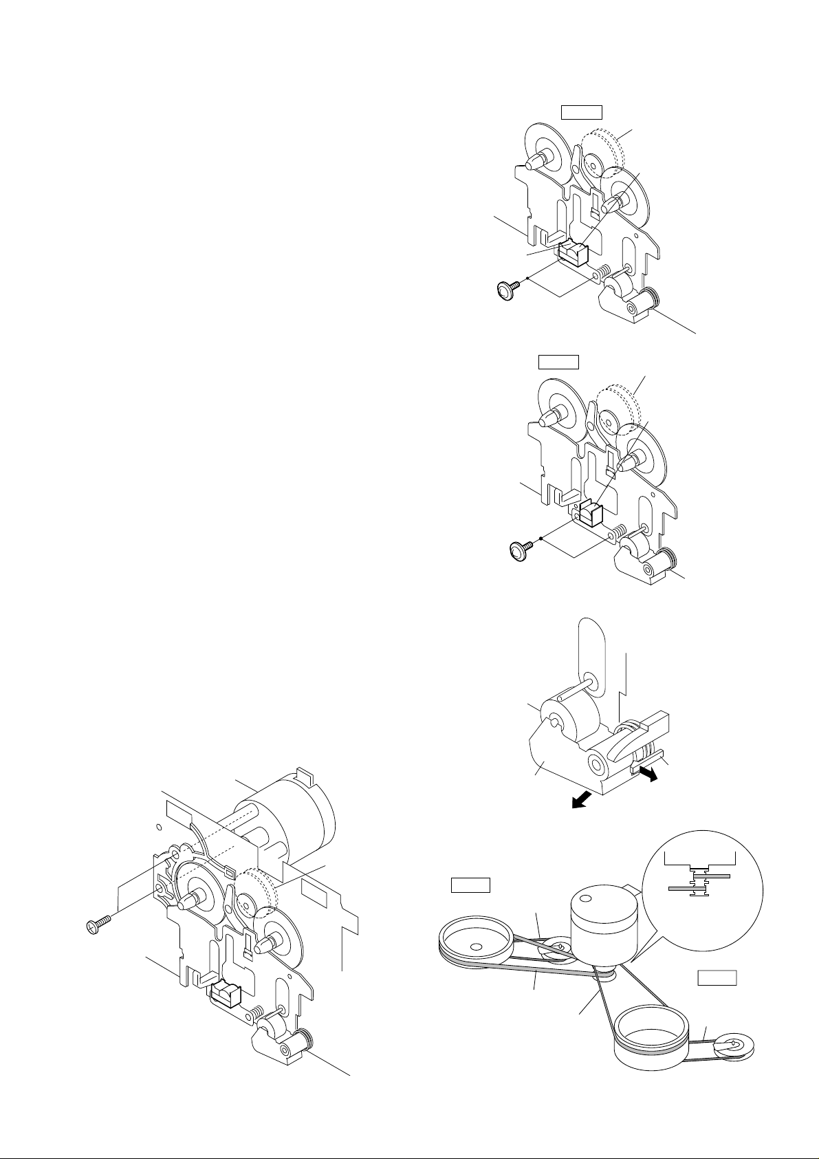
ADJUSTMENT
MECHANISM SECTION
• Driving Force Check
Torque Meter Specified Value
Play: TW-2111 Tape 1: Over 80 g
Tape 2: Over 80 g
• Torque Check
Torque Meter
Play: TW-2111 30 to 80 g.cm 30 to 80 g.cm
Fast forward: TW-2231 — 70 to 180 g.cm
Rewind: TW-2231 — 70 to 180 g.cm
Specified Value
Tape 1
Tape 2
• Tape Speed
Test Tape
Normal MTT-111 Variable 3,000 ± 30 Hz Speaker
speed Resistor in Terminal
Adjusting
Point
motor. (Load
Specified
Value
Instrument
Connection
resistance:
6 ohms)
TAPE MECHANISM
Tape
Motor
Variable Resistor in motor
Figure 16-1
• FM mute level adjustment
FM signal oscillator Frequency 1 kHz, 22.5 kHz
Frequency
Adjusting
method
98.0 MHz 26 dB(EMF) VR351 Input: CNP301
CNP301
FM signal oscillator
Adjusting
object
UNIT
Adjusting object
Output: Speaker
Terminal
Speaker
Terminal
Electronic
Voltmeter
Figure 16-2 FM Mute Level
• Erasing the registered broadcast station
When the power is off, press and hold the TUNER (BAND)
button and the X-BASS button, and then press the POWER
button.
All the registered stations are erased.
• Setting the Test Mode
While holding down the MEMORY/SET button and the XBASS button, press the POWER button. Frequencies are
rewritten in memory as shown in table 16. Call them using
the VOLUMN knob of tuner circuit adjustment and check.
Note that once you reinitialize the settings, the frequencies
recorded by users will be changed.
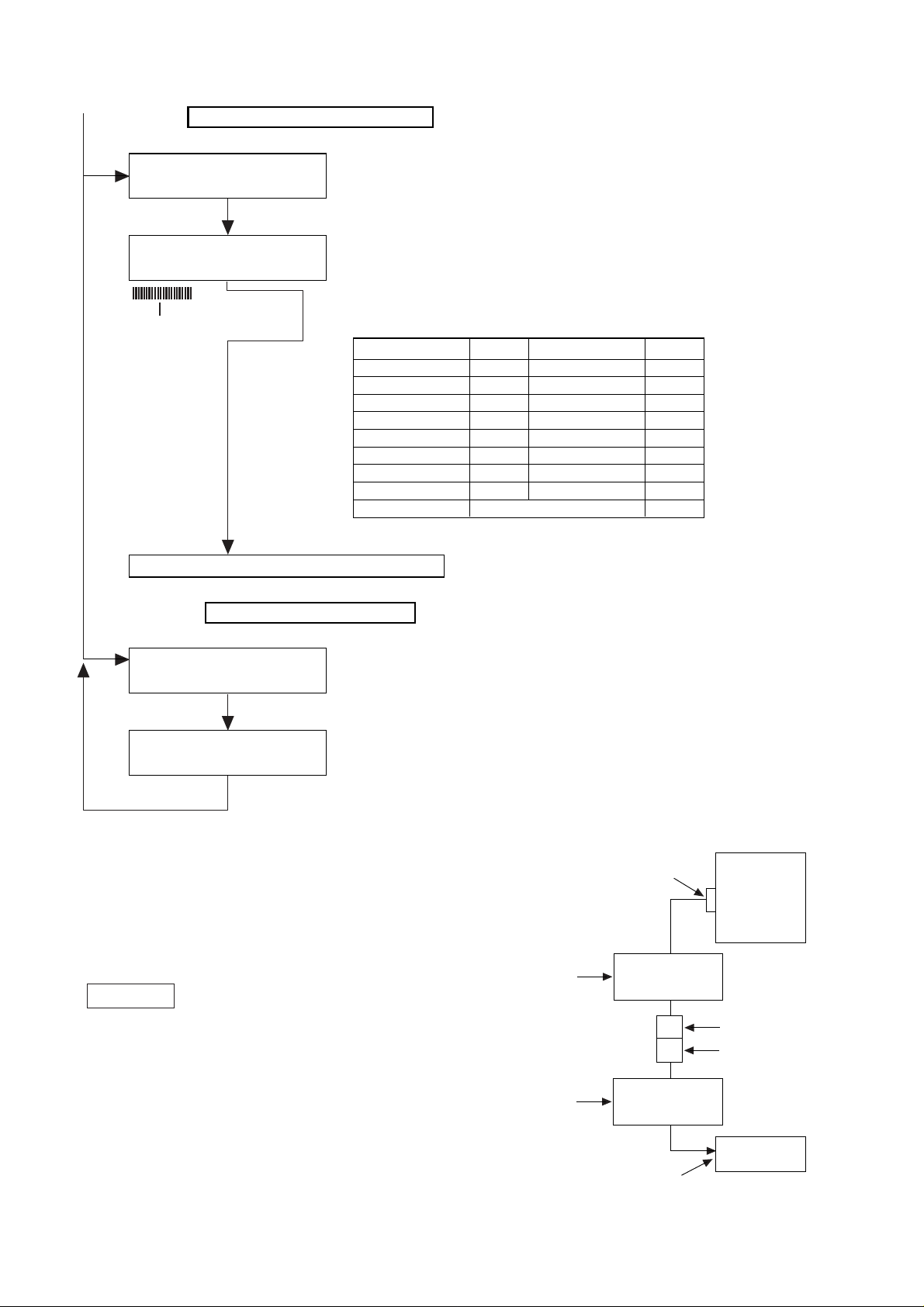
Preset No. Frequency
P01 87.5 MHz P06 530 kHz
P02 108.0 MHz P07 1,720 kHz
P03 90.0 MHz P08 600 kHz
P04 106.0 MHz P09 1,400 kHz
P05 98.0 MHz P10 990 kHz
Preset No.
Frequency
Table 16
TUNER SECTION
fL: Low-range frequency
fH: High-range frequency
• AM adjustment and confirmation
AM signal oscillator Frequency 400 Hz, 30 %, AM modulation
Adjusting item
IF Adjust the indication of Set IF wafeform
Frequency cover fL: T306 (530 kHz) fL: 1.3 ± 0.1 V
(VT line voltage of Adjust the indication fH: 8.5 ± 1.3 V
TP301) of set to 530 kHz. (Only confirmation)
Tracking fL: T302 (990 kHz) Set the output of
Adjusting object
T351 set to 1,720 kHz.
fH: (1,720 kHz)
Adjusting
method
450 kHz to maximum.
speaker terminal
to maximum.
AM signal oscillator
– 16 –
AM Loop Antenna
Loop Antenna
IF : Speaker Terminal
Frequency cover: TP301
UNIT
Figure 16-3 AM IF
Electronic
Voltmeter
GND
Page 17
MAIN PWB
CNP301
FM/AM LOOP
ANTENNA
CD-DVD500
R345
TP301
FM MUTE
LEVEL
Figure 17 ADJUSTMENT POINTS
DVD/CD SECTION
• Adjustment
Since this DVD/CD system incorporates the following
automatic adjustment functions, readjustment is not needed
when replacing the pickup. Therefore, different PWBs and
pickups can be combined freely.
Each time a disc is changed, these adjustments are
performed automatically. Therefore, playback of each disc
can be performed under optimum conditions.
FE301
T351
AM IF
VR351
R350
T302
AM
TRACKING fL
AM BAND
COVERAGE fL
TP302
T306
– 17 –
Page 18
CD-DVD500
t
m
DVD TEST MODE
DVD Test Mode Pressing down the DVD/CD button and X-BASS/DEMO button, press POWER button.
ROM Renewal Mode Pressing down the DVD/CD button and EQUALIZER button, press POWER button.
[DVD TEST MODE]
Test mode initial image plane
F0000000 *00#####
<The "1" key of the remote controller is pushed.>
(* is a region number)
(##### is a program version)
The preparation date display of the program
10000000 ********
(Last updata)
The "Playback" key of the remote controller is pushed.
Model number display
10000001 *******#
(Model number)
The "Playback" key of the remote controller is pushed.
The version display of the program
10000002 ********
(Program ver.)
The "Playback" key of the remote controller is pushed.
Reagion number display
10000003 0000000*
(Region code:Binary display)
The "Reactivation" key of the remote controller is pushed.
Micro-code number display
10000004 ********
(Microcode ver.)
The "Playback" key of the remote controller is pushed.
The preparation date display of the servo program
10000005 ********
(Servo ver.)
(* is a model number) (# is a region nu
DVD500: 0000500#
DVD200: 0000200#
(* is a region number)
Micro-code is the thing of the process
program of the system integrated circui
It is returned to the test mode initial image plane.
<The "2" key of the remote controller is pushed.>
Color bar display
20000001 00000000 (FIP)
It is returned to the test mode initial image plane.
<The "3" key of the remote controller is pushed.>
To (1)
Dynamic Test
30000000 00000000
The "Playback" key of the remote controller is pushed.
There is no copy guard signal.
As for the symptom when it was
dubbed in the video tape recorder?
The "Stop" key of the remote controller is pushed.
– 18 –
Page 19
From (1)
(2)
<The "1" key of the remote controller is pushed.>
DVD laser lights, the spindle motor
rotates and the pickup moves to the
outer periphery.
30000001 000000DD
<The "1" key of the remote controller is pushed.>
DVD laser off, CD laser on, spin kick,
sled outer periphery feed
ErrDisplay0 ErrDisplay1
30000001 000000CD
<The "1" key of the remote controller is pushed.>
Laser off, spin kick, sled outer periphery
feed
ErrDisplay0 ErrDisplay1
30000001 00000000
<The "1" key of the remote controller is pushed.>
It is returned to the Dynamic test.
CD-DVD500
Note: Not to face the light of the laser squarely,
caution!
<Disk is put, and the "2" key of the remote controller is pushed.>
*It is usually returned in power source off for the state.
STEP TEST
30000201 00000000
The "PLAY" key input.
STEP TEST
30000202 00000000
The "PLAY" key input.
STEP TEST
30000203 00000000
The "PLAY" key input.
STEP TEST
30000204 00000000
The "PLAY" key input.
STEP TEST
30000205 00000000
The "PLAY" key input.
STEP TEST
DD000210 00000000
Focus on
RF gain adjustment, Track on
Focus gain adjustment
Track gain adjustment
Focus balance adjustment
STEP TEST
3000E201 000000EE
When a disk is not in.
(In case of CD)
STEP TEST END
CD000210 ********
(******** is sub-Q.)
After TOC Reading,
Follow-up play condition
STEP TEST
DD000211 00000000
The "PLAY" key input.
STEP TEST END
DD000212 ********
(******** is the sector ID.)
The "Stop" key of the remote controller is pushed.
It is returned to the Dynamic test.
To
Focus balance of the layer 1,
follow-up play condition after focus gain adjustment
– 19 –
Page 20
CD-DVD500
From (2)
"3" Key input
PLAY TEST
30000001 00000000
Following playback, jump test mode
Because a tray opens, adisk is published.
"Open/Close" Key input
PLAY TEST
DD######*********
Error rate lever ver
1ber=5error
It is returned to the test mode initial image plane.
Spin offset adjustment mode
"TOP MENU" Key input
SPIN OFFSET
It becomes following play state.
(******** is a sector ID.)(###### is a error rate)
A test jump can be done by inputting the following key
from the remote controller.
Key Jump Key Jump
1-131
4 -102 6 102
7 -510 9 510
Clear -511 Enter 511
2 -765 Repeat 765
5 -766 A-B 766
8 -7000 Program 7000
Before skipping. -15000 After skipping. 15000
>10 Layer Jump
The"Stop" key of the remote controller is pushed.
PLAY TEST
00000000 0000*****
(**** is a adjustment result.)
[DVD ROM RENEWAL MODE]
1. A DVD itself and a personal computer are articulated as
the right figure for. Sofrware the renewal is started more.
2. Pressing down the DVD/CD button and EQUALIZER button,
press POWER button.
WRITE It is displayed.
3. Start a data transfer within 5 seconds -30 seconds after
you go into DVD ROM RENEWAL MODE.
4. AC code is removed after a data transfer is finished.
5. AC code is put again, and it is within DVD test mode,
and program vergion is confimed.
Fixture for the
ROM renewal
Adapter cord
RS232C
Personal computer
(DOS)
RUNTK0808GEZZ
RCA PIN PLUG
RCA PIN JACK
QCNWK0001AWZZ
Unit
Molex 2pin conector
Figure 20
– 20 –
Page 21
Standard Specification of Stereo System Error Message Display Contents
Error Contents DISPLAY Notes
Output while Device Protection Operation. TIMER LED 00: While in Protect Circuit Operate.
01: Over Current Detection.
02: DC Detection.
03:
TAPE Mechanism Error. 'ER-TA**' 00: Tape Mechanism Error.
01: Initial Error.
02:
03:
DVD/VCD Pickup Mechanism Error. 'ER-CD**' 00: Pickup Mechanism Error.
01: PU-IN SW Detection NG.
02:
03:
04:
CD Changer Mechanism Error. 'ER-CD**' 10: Changer Error.
11: Initial Error.
12:
13:
Tray Error. 'ET-CD**' 20: Tray Error.
21:
22:
23:
Focus Not Match. 'NO DISC'
Communication error. 'ER-CD**' 30: DVD Error.
TUN PLL Unlock. 'ER-TU**' 00: TUN Error.
01: PLL Unlock.
02:
03:
CD-DVD500
Notes for handling the mechanism unit
Since the pickup semiconductor laser can easily damaged by
the static electricity, handle the mechanism unit with care.
To prevent damage by the static electricity during
transportation, the LD terminals are short-circuited at 2 points
on the PWB. Unsolder them by a soldering iron after
completing the connection. When you return the mechanism
unit, solder the terminals again.
Soldering on the
Flexible PWB
4X
mechanism PWB (two points)
DVD Motor PWB
Figure 21
– 21 –
Page 22
CD-DVD500
O
0
K
P
3
4
O
D
V
U
D
HOLOGRAM
LASER UNIT
GND
HOLOGRAM
LASER UNIT
M1
SPINDLE
MOTOR
PICKUP IN
M2
SLED
MOTOR
OPEN/CLOSE
SW3
DISC NOMBR
M3
T/T UP DOWN
LOADING
MOTOR
ACTUATOR
–
+
–
+
–
+
–
+
(DVD)
OSC
–
+
–
+
–
+
–
+
–
+
(CD)
SW4
SW2
SW2
CAM
TO DISPLAY
FO+
TR–
TR+
FO–
LD
PD
VA
VB
VC
VD
Vref
Vcc
GND
Vcc
Vcc
VA
VB
VC
VE
VF
Vref
GND
LD
PD
M
M
M
UNIT
1
2
3
4
5
6
7
8
9
10
11
12
13
14
15
16
17
18
19
20
21
22
23
24
25
26
27
28
29
30
CP3202
LD_FWD
LD_RVS
DVD_FUNC
CAM_SW
DISC1_SW
UART_RX
DVD_BUSY
DVD_DI
DVD_DO
DVD_CLK
DVD_STB
D_GND
IC3301
TA1323F
TR+
FO+
TR-
FO-
+B9
+B9
Q3303
LDOI
46
MDI1
45
P1DI
52
P1CI
53
P1BI
54
P1AI
55
P2AI
58
P2BI
59
P2CI
60
P2DI
61
P2FP
63
P2FN
64
P2TP
2
P2TN
3
PITP
47
PITP
48
VrA
42
DFTN
22
SCB
13
SCL
14
SCD
15
VDD
8
RF SIGNAL PROCESSOR
51
LDP1
CD_LD
APCI
R-GAIN
ADJUST
F-GAIN
ADJUST
T-GAIN
ADJUST
BUS
DVD_LD
APC2
MDI2
LDO2
1,39,56,62
4
5
Q3302
FLGA
Q3301
LDP2
57
RF RIPPLE
CREATION
DPDTE
CREATION
FE
CREATION
3BTE
CREATION
DPAC
EQ
LEVEL
DETECT
DPBD
DPD1
IC3705
NJM2904M
OPE AMP.
+B8
5
6
8
7
9
4
3
C3207
2
–
1
+
3
5
+
7
–
6
+
14
–
SLN
+
13
–
SLP
+
12
–
SPN
+
11
–
SPP
+
17
–
FON
+
18
–
FOP
+
15
–
TRN
+
16
–
TRP
8
VCC
9
LDN
10
LDP
19,29,30
GND
BA5984FP
MOTOR DRIVER
OUTR
OUTL
+B10
+
–
SHIFT
LEVEL
+
–
SHIFT
LEVEL
+
–
SHIFT
LEVEL
SHIFT
+
–
SHIFT
LEVEL
IC3801
LOADING DRIVER
13
3
6
1
8
14
IC3201
74HC07AF
BUFFER AMP.
+
–
+
–
+
–
+
–
+B10
FWD,REV
12
MUTE
BIAS
OPOUT1
OPIN1(–)
–
+
OPIN1(+)
OPOUT2
OPIN2(–)
–
+
OPIN2(+)
OPOUT3
OPIN3(–)
–
+
OPIN3(+)
OPOUT4
OPIN4(–)
–
+
OPIN4(+)
4
5
2
9
7
1,28
DPD2
1211109
21
20
4
3
2
7
6
5
22
23
24
25
26
27
18,23,31,36
FE-GAIN
ADJUST
TE-GAIN
ADJUST
CONSTANT
VRCK
VRCK
+B9
RPO
RPZ
RFOP
RFON
DPDB
TIME
ADJUST
16 17
6
+B10
EQF
EQB
FEO
TEO
26
25
30
29
44
43
33
TEB
35
21
20
19
LVL
VCKF
7
1
SLDRV
5
SPDRV
FOD
TRD
2
IC3507
BR93L66F
EEPROM
3
6
5
4
7
LVL
RFRP
RPZI
RFOP
RFON
EOF
EOB
TEB
DPDC
SLDRV
SPDRV
FDD
TRD
SPV
FLGA
VRCK
SCB
SCL
SCD
/DFTN
+B10
5
42,3
IC3503
PST9129N
RESET
UART-RXD
KEY3
S/E_DI
S/E_DO
S/E_CK
FIP_CS
EECS
+B10
138 PVDD
ADC
150
FEI
FEI
151
TEI
TEI
LVL
RFRP
RFZI
RFCD
RFDVD
RFON
DAC IF
(PWM)
ANMON
EQBC
TEBC
DPDC
FMO
DMO
DAC
FOO
TRO
EXT_DA
ID
DETECT
MEMORY CTL
AVSS
DEQ
DIGITAL SERVO
DATA
SLICER
AVSS 149,154
PVSS 127
XVSS 9
DACVSS 3,8
VSS5 17,22,39,66
61,83,110
VSS3 105,122,171
ERROR
DETECT
RAM
(4.2KByte)
VCC
152
153
146
142
143
139
168
167
164
166
162
163
158
159
156
37 FLGA
170 VRCK
174 SCB
173 SCL
172 SCD
169 /DFCT
+B10
1,11,26,40,62,76,86
VDD1
IC3508
IX1761GE
TRACK BUFFER I/F
71 G_RESET
73 /RESET
67 CHOP
90 MUTE
100 EJ_SW
68 LD_SW
61 IN_SW
70,69 LD_FWD/REV
56 UART_RXD
97 KEY3
55 SUB/EEP_DIN
53 SUB/EEP_DOUT
57 SUB/EEP_CLK
S/E_CS
87
EECS
62
1,33,52,76,81
AVCC
93
6,15,24,38,47,59,79,104
103
SERVO
CONTROL
45,51,64
VSS
5 DAC VDD
144,160 AVDD
SLICE
LEVEL
GEN.
PLL
MICOM I/F
+B10
VDD2
777991 7880929394
+B10
MD0-7
MD0-7
46-53
72-65
5VBUS
N0O-N7O
HADR0-7 HDAT
SYNC
DEMOD
TC9
SERV
PSYCO
MICR
V
X
IC
/
PDC
73
/SVAL_O
SOSO_O
41
PD
I
IX
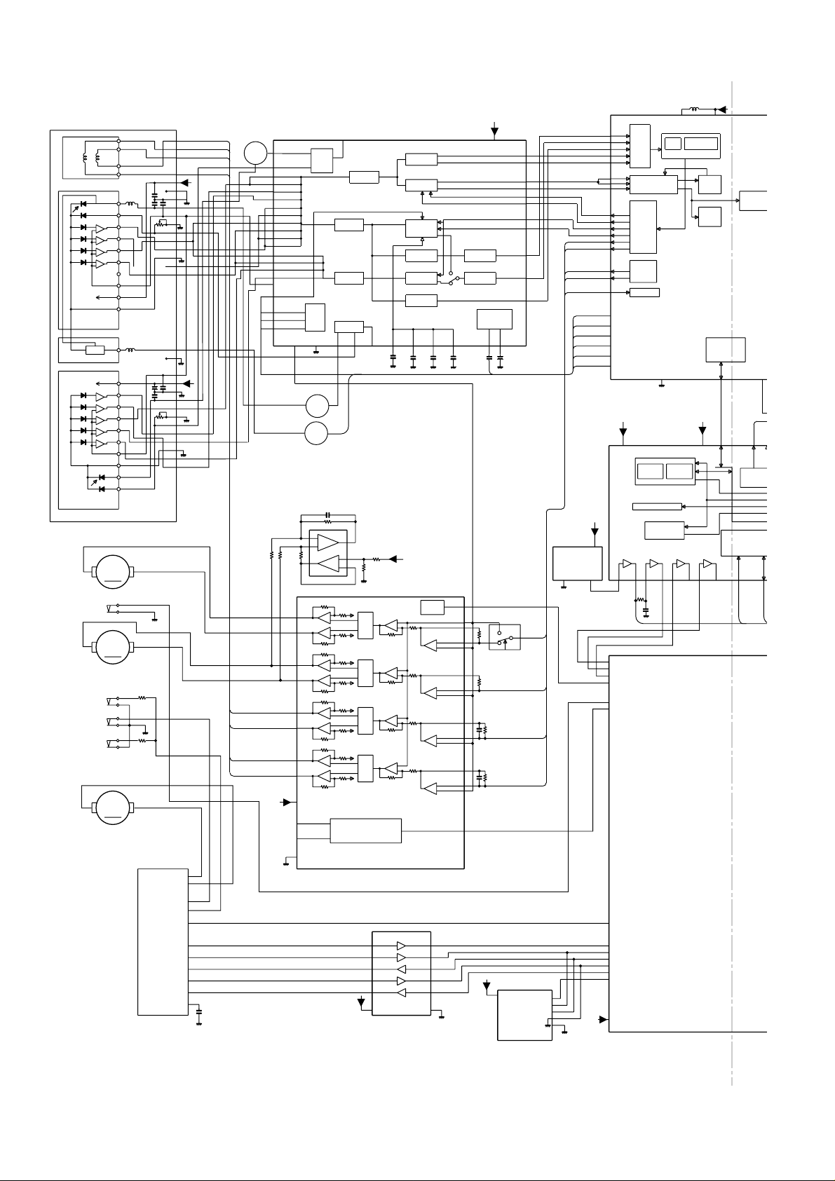
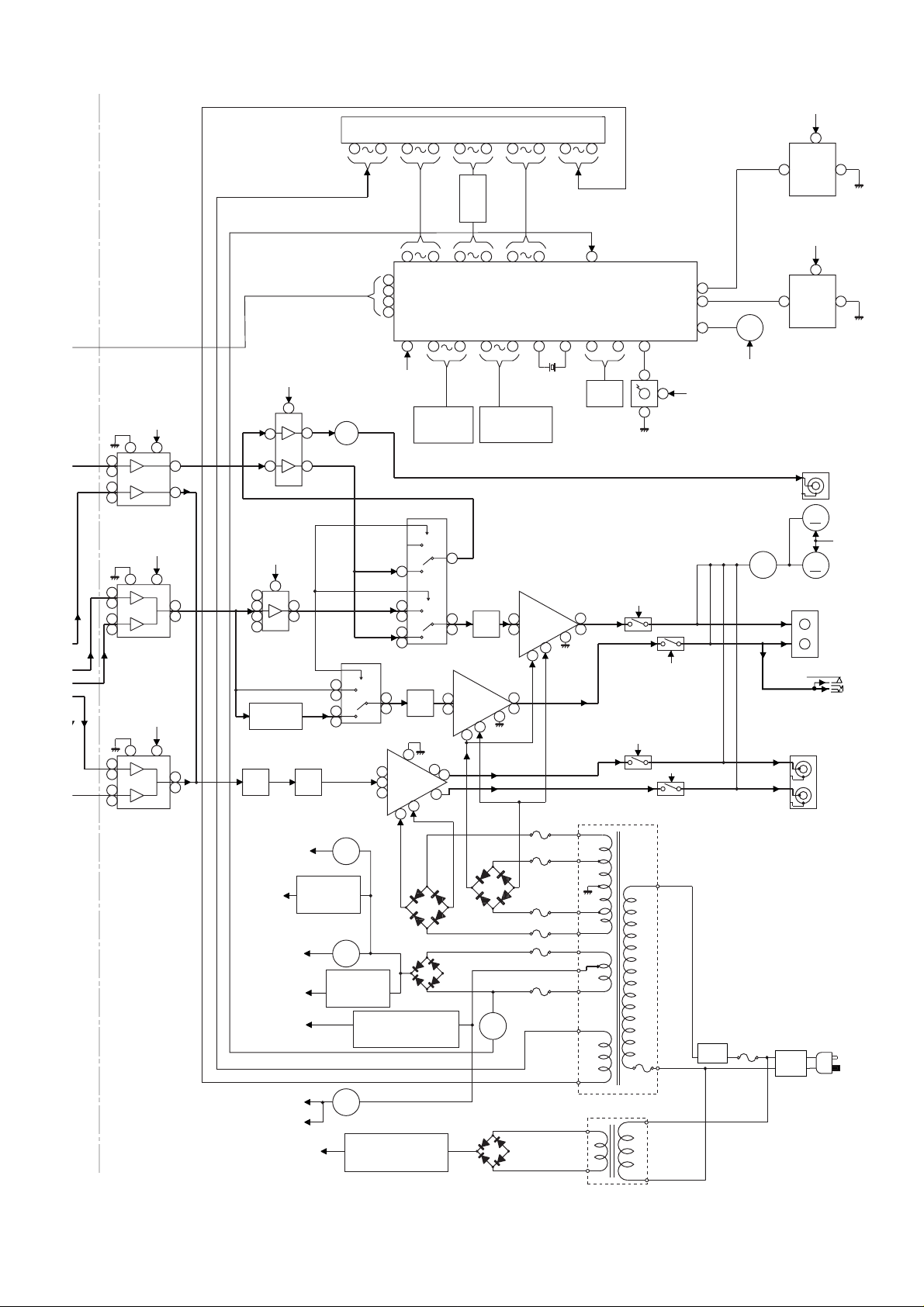
Figure 22 BLOCK DIAGRAM (1/4)
– 22 –
Page 23
CD-DVD500
+B10
+B10
DAC VDD
,160 AVDD
L
E
EL
.
L
ICOM I/F
MD0-7
7
VDD3 16,33,59
78,89,116
XVDD 12
SYNC DET.
DEMODULATION
IC3701
TC94A03F
SERVO ECC
/PDRQ
MD0-7
PDCK
46-53
72-65
5VBUS
N0O-N7O
HADR0-7 HDAT0-7 HRD HWR HAS HCS1 HCS2
MICROCOMPUTER
/PSYC
73 72 71
SDCK_O
/SVAL_O
SOSO_O
41 42 43 47 48 49
TIMING GEN.
HOST I/F
IC3504
IX1687GE
VDD5 54,74,95
OUTPUT I/F
PD0-7PDB
70
SDCK_I
/SVAL_I
PDRQI PDRQO
+B10
DRAM
60,62-65,67-69
PSYCI PDCKI PDCKO PSYCO
96-104
106-109,111-113
79-82,84-88
I/F
ECC
SD0_1,SD7_1
/SOSO_I
/HWR,FROM_CS,/RD 84,120,83
92,93
91
90,94
10
11
XO
/MCE 44
/MDR,/MWR
42,43
/MA 41
/MINT 45
/RST 40
52 53-60
PDI(0)-(7)/ERR_1
IPD I/F
OPD
I/F
PDON0O-N7O
PDON8O
VSS 10,25,29,39,44,50
61,63,75,85,100
AV-CS
HGA_INT
AV-INT
Z_STNBY
Z_RESET
/MA
SRV_CS
WAIT
/SRV_INT
VMUTE
S1_H
UART_CTL
UART_RXD
AMUTE2
ADAC_L
ADAC_CK
ADAC_DA
HGA_CS
A0-19 2-5,7-14,16-23
D0-15 34-37,39-46,48-51
/HWR,RAS 84,118
LCAS,CAS 86,116
DDAT0-15
DADR0-8
UCAS/LCAS
RAS
OE/WE
XI
FL3701
(22.5792MHz)
EXTAL
30-37
XTAL
119
26
30
64
65
66
117
92
31
109
108
58
56
88
112
111
110
60
77
78
38
A1-9
D0-15
/WA,RAS
LCAS,CAS
FL3501
(20MHz)
/WR,FRCS,/RD
IC3702
IX0447AW
4M EDO DRAM
2-5,7-10,31-34,36-39
16-19,22-26
28,29
14
27,13
/ERR_0
SDCK_O
/SOSO_O
/SVAL_O
SD0_O-SD7_O
+B10
+B10+B10
+B10
+B10
/WA,RAS
LCAS,CAS
D0-15
/RD,/WR
AVCS
WAIT
AVINT
Z_STNBY
Z_RESET
L3602
L3601
FB3605
FB3604
A1-9
D0-15
A1-19
D0-15
FL_RESET
1,6,20
21,35,40
151
N.C
147
150
148
149
152-159
25-20
18,17
15,13
11,9-5
30-27
A1-4
31,34
32
39
2
1
4
36
N.C
37
134
N.C
145
143
N.C
122
124
160
N.C.
3,16,26,38,44,52,58,67
71,77,83,89,94,98,126
135,140,19,99
130
104
12,33,63,116,142
121
113
N.C
136-138
N.C
131
N.C
139
N.C
141
N.C
133
101,107,109,110
123,132
10,40,49,56,65,69
80,86,97,128,145,146
14,35,73,114,144
A0-8
16-19,22-26
DQ1-16
2-4,7,8,31-34,36-39
WE,RAS
13,14
LCAS,UCAS
29,28
A0-18
16-25,1-8,48
DO1-16
29-36,38-45
WE,/CE,/OE/WR,FRCS,/RD
11,26,28
12 RP
+B9
R3613
N.C
127
VCLKX2
DVD-DSP
I/F
DVDREQ
DVDERR
DVDSTRB
DVDSOS
DVDVALID
DVDDAT0-7
HOST
I/F
HD0-15
HA0-3
HWR,HRD
HCS
HACK
HWID
HORD
HTYPE
HRDY
HIRQ
GENERAL
PURPOSE
GPIO
GPIS
GPSO
RESET/
STANDBY/
STATUS
I/F
STNBY
RESET
IDLE
DIGITAL
AUDIO
I/F
AIN
AOUT0-3
AMCLK
ALRCLK
ABCLK
S/PDIF
IC3601
IX1720GE
DVD DECODER
IC3502
IX0448AW
4M DRAM
VCC,VPP 37,13
IC3501
IX1689GE
FLASH ROM
X3601
27.0MHz
R3612
119
XO
PLL/CLOCK
I/F
PLLCFG-I
PLLCFG-O
CVBS/G/Y
ANALOG
VIDEO
ENCODER
I/F
CVBS/C
CQSYNC
TEST-SIO
I/F
ICEMODE
SCNENBL
TESTMODE
DIGITAL
VIDEO I/F
HSYNC
VSYNC
SDRAM
RAMME
I/F
RAMCAS
RAMRAS
RAMCS0,1
RAMDOM
RAMDAT0-15
RAMADD0-11
91,88,85,82,79
76,74,70,88,72
75,78,81,84,87
90
VCC 1,6,20
OE 27
VSS 21,35,40
WP 14
BYTE 47
RY/BY 15
VSS 27,46
GCLK
Y/R/V
C/B/U
RSET
VREF
VCLK
PCLK
120
GCLK
FI
N.C
+B10
112
125
129
50,47,45
42,41,43
46,48,51
54,53,55
+B10
62-60
57,59
R3552
R3555
102
105
106
103
108
111
100
117
115
118
92
95
93
96
68
64
D_1.8V
D_3.3V
Q3205
Q5001,5004
BUFF.
Q5007,5010
CVBS
L.P.F
Q3203
BUFF.
Q5002,5005
Q5008,5011
Y
L.P.F
Q3202
BUFF.
Q5003,5006
Q5009,5012
C
L.P.F
R3603
R3604
N.C
N.C
+B10
N.C
N.C
N.C
N.C
RAMWE,RAMCAS
RAMCS0(FOR IC3602)
RAMCS1(FOR IC3603)
RAMD0-15
RAMA0-11
1.8V RGE
3.3V RGE
+B7
RAMRAS
PCLK
RAMDOM
M_GND
A_GND
D_GND
IC3662
IC3661
IC3602/3603
IX0449AW
16M SDRAM
15-17 WE,CAS,RAS
18 CS
35 CLK
14,36 LDOM/LDOU
DQ0-15
2,3,5,6,8,9,11,12,39
40,42,43,45,46,48,49
A0-11
21-24,27-32,20,19
A_5V
D_5V
M_8V
SO7001
VIDEO OUT
J7002
S-VIDEO
IC501
TORX178A
DIGITAL OUT
+B10
1,7,13,25,38,4434 CKE
VSS
4,10,26
41,47,50
CP3201
A_5V
D_5V
M_GND
A_GND
D_GND
M_8V
V_8V
+B10
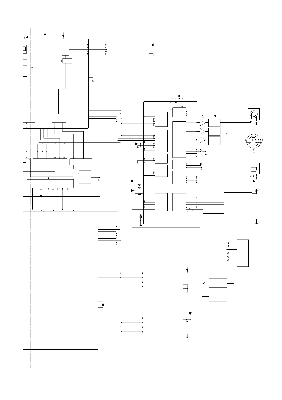
Figure 23 BLOCK DIAGRAM (2/4)
– 23 –
Page 24
CD-DVD500
N
F
B
B
6
5
3
2
6
5
3
2
6
5
3
2
AM
FM
CNP301
8
6 7
AM TRACKING
FE301
FM FRONT END
5
4 32
VCC
+B4
10.7 MHz
450 kHz
CF303
1
T351
CF352
AM IF
AM MIX
21
IC303
LA1832S
FM IF DET./FM MPX./AM IF
AM RF IN
AM OSC IN
21
23
7
FM/AM
OUT
18
4
AM IF
CF351
5
9
8
GND
FM+B
MPX IN
FM/AM
16
X351
456kHz
17
13
VCO
MO/ST
R
L
12
14
15
PLAYBACK
HEAD
TAPE 1
RECORD/
PLAYBACK HEAD
TAPE 2
L-CH
R-CH
L-CH
R-CH
VIDEO IN
REC
P.B.
AC BIAS
T303
JK601
AUX
T306
FROM CD SECTION
1
BA3126N
3
SELECTOR
6
+B4
2
AM BAND
COVERAGE
L
11
TUNER
14
R
L
9
AUX
16
R
L
10
TAPE
15
R
IC102
HEAD
5
8
SWITCHING
CNP7
IC501
TORX178B
OPTICAL FIBER
DATA LINK
+B4
23
IC601
LC75341
AUDIO PROCESSOR
VSS VDD
3
9
7
4
POP REDUCE
X352
4.5 MHz
VT
20
PLL(TUNER)
+B4
L
4
21
R
PLAYBACK AND RECORD/
PLAYBACK AMP.
L(T1)
R(T1)
L(T2)
R(T2)
L NF
R NF
L REC
R REC
REF
1
OSC
IC302
LC72131
Q360
+B5
3
2
AN7345K
1
24
2
23
3
22
6
T1/T2
9
16
14
NOR/
15
HIGH
FM
1
IC101
REC
12
X501
22
7
12
2.2MHz
H/N
T1/T2
19
15
+B5
9
13
35
49
62
81
95
97
98
99
13
20
18
17
10
STEREO
CLK DODI
CE
5
11
43
16
FM/AM
MO/ST
21
10
9
14
VCC
IC502
74VHC00F
INVERTOR
GND
7
+B5
24
53
71
VSS
VDD
VDD
VSS
VSS
VSS
VSS
VSSDL
IC504
VSSX
IX0443AW
DOLBY DECODER
XO
XI
+B4
4
PB
L
R
21
5
7
8
L
R
L NF
R NF
ALC
REC
REC
MUTING
Q121
Q122
VDD
6
17
IC602
M62446FP
6-CH ELECTRONIC
VOLUME
+B4
42
36
SW_OUT
DVDD
C_OUT
33
SWIN
6
SR_IN
8
SL_IN
9
C_IN
11
R_IN
13
L_IN
15
GND_R
12
L_OUT
R_OUT
SL_OUT
SR_OUT
31
32
34
35
4
9
39
IC505
AK4527BVQ
6-CH CODE
+B4
37
16
ROUT2
DVSS
ROUT3
LOUT3
LOUT2
ROUT1
LOUT1
RIN+
LIN+
30
32
36
26
24
23
25
28
27
6
34
RX
14
18
22
47
CKO
BU
MOTOR
DRIVER
+B3
Q102
ERASE HEAD
BIAS OSC
Q128
L104
SWITCHING
Q101
SWITCHING
Q124
L103
Q102
BIAS
Q126
TO IC181
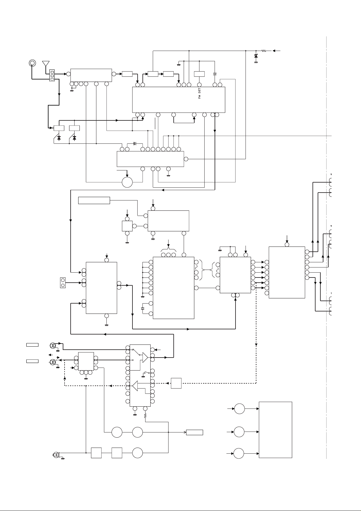
Figure 24 BLOCK DIAGRAM (3/4)
– 24 –
TAPE 1
SOLENOID DRIVER
Q102
+B3
TAPE 2
SOLENOID DRIVER
Q102
+B3
TAPE
MECHANISM
ASS'Y
Page 25
IC606
NJM4565M
BUFFER AMP.
+B4
4
3
2
5
6
IC605
NJM4565M
BUFFER AMP.
+B4 7 V
4
3
2
5
6
IC607
NJM4565M
BUFFER AMP.
+B4
4
3
2
5
6
CD-DVD500
+B5
FL701
13
93
AVDD
PSEANA
3
IC703,IC704
KIA4558P
OPE AMP.
IC906
MUTE
Q906
Q907
R
10
18
6
9
–B1
D806
FL DISPLAY
14
92
5
14
4
15
L
IC901
15
STK40270N
POWER AMP.
1
R
L
+B2
D805
D881
D882
6
31
VF2
100
CE
28
29
CLK
30
DI
31
DO
1
+B4
IC907
KIA4558P
OPE AMP.
8
1
7
8
1
7
8
1
7
3
5
+B4
2
3
5
6
IC904
KIA4558P
OPE AMP.
HIGH PASS
FILTER
20ATT
Q401
Q402
Q407
+B8 M_+8V
+B7 V_+8V
+B3 M_+12V
+B4 A_+10V
+B9 A_+5V
+B10 D_+5V
8
8
SYSTEM
+B5 5V
+B6 5V
SYSTEM
1
7
1
7
13
TRIPLE 2-CH
MULILPEXER
MUTE
Q403
Q404
Q408
IC852
KIA7808AP
VOLTAGE
REGULATOR
REGULATOR
-VF
VF2
VF1
MUTE
Q917
3
5
12
IC905
TC4053BP
Q419
Q850
IC850
KIA7810AP
VOLTAGE
Q418
CONSTANT VOLTAGE
+B6
TC4053BP
TRIPLE 2-CH
MULILPEXER
13
3
1
2
5
SYSTEM
4
14
13
IC401
1
STK40224
15
POWER AMP.
16
8
+B1
D802
D803
D804
IC851
KIA7805AP
CONSTANT VOLTAGE
REGULATOR
IC880
KIA7805AP
REGULATOR
29
19
Q701
Q702
Q703
Q704
Q705
Q706
87
86
IX0442AW
SYSTEM MICRCOMPUTER
KEY
7
9
KEY
SW701-SW712
SW714-SW716
SW722-SW729
SW731-SW734
SYSTEM
MUTE
L
1
Q905
Q908
15
R
10
6
13
9
8
–B2
D801
F805
6.3A/125V
F806
4A/125V
F807
4A/125V
Q806
D884
D883
53
60
IC701
X1
16
XL701
4.194304 MHz
IC902
STK40270N
POWER AMP.
9
8
L
R
F804
6.3A/125V
F802
4A/125V
F803
4A/125V
56
-VF
X2
17
13
MAIN POWER TRANSFORMER
SUB POWER TRANSFORMER
6
10
58
VF1
79
VLOAD
JOG_0
25
JOG701
JOG
VOLUME
L
R
26
T802
JOG_1
RY902
RY402
T801
REMOCON
27
1
3
2
REMOTE SENSOR
+B3
RY901
+B3
T.F.
+B3
+B3
LCK1
LCK2
RESET
RX701
+B6
RY401
49
48
42
RY801
RESET
Q707
+B5
FAN MOTOR
DRIVER
F801
6.3A/125V
Q423
18
VDD
LCK
4 1
VSS
IC702
BU2092F
INPUT/OUTPUT
EXPANDER
+B5
18
VDD
LCK
41
VSS
IC181
BU2092F
INPUT/OUTPUT
EXPANDER
SOC901
SUBWOOFER
PRE OUT
M401
M
FAN MOTOR
+B3
M402
M
FAN MOTOR
SO901
SPEAKER
TERMINAL
SUBWOOFER
MAIN
JK701
HEADPHONES
SOC401
SPEAKER JACK
SURROUND
CENTER
AC POWER
SUPPLY CORD
L802
LINE
FILTER
AC 120 V/60 Hz
Figure 25 BLOCK DIAGRAM (4/4)
– 25 –
Page 26
CD-DVD500
0
B
N
ASLCO
3
4
R3740 47K
A
B
FW2
C
D
E
CNS5
F
TO
JOINT PWB
P42 3-A
G
DVD SERVO PWB-C (1/3)
Q3301
KTA1504 Y
R3310
4.7K
R3314
C3306
R3303
0.01
PICK_UP
50
49
48
47
46
45
44
43
42
41
40
39
38
37
36
35
34
33
32
31
30
29
28
27
26
25
24
23
22
21
20
19
18
17
16
15
14
13
12
11
10
9
8
7
6
5
4
3
2
1
CS3301
TR+
FO+
TR–
FO–
VCC
GND
GND
LD
V/2
VR
PD
VC
VA
GND
VB
VD
VOSC
GND
V/2
VCC
GND
LD
VC
VR
PD
VA
VE
GND
VF
VB
LD–
LD–
LD+
LD+
DISC1_SW
GND
CAM_SW
LD/EJ_SW
SP+
SP+
SP–
SP–
IN_SW
GND
SL–
SL–
SL+
SL+
2.2K
TR+
FO+
TR–
FO–
C3302
+B
1
C3303
1
C3304
1
+B
C3305
1
R3906
15K
R3905
8.2K
IN_SW
LD_RVS
LD_FWD
C3301
1
R3343
Q3302
1
+B
47
47
C3307
R3346
100/6.3
R3315
470
2SA1955 A
R3344
3.3M
R3311
IC3801
BA5984FP
MOTOR
DRIVER
0.01
C3802
+B
D3301
DAP202K
2
1
3
1
+B
49
50
51
52
53
54
55
56
57
58
59
60
61
62
63
64
14 13 12 11 10
SLP
SLN
SPIN–
IC3801
BA5984FP
10/16
C3803
TRN
TRP
FON
15 16 17 18 19 20 21 29 22 23 24 25 26 27 28
FO+
FO–
TR–
TR+
47
47
C3319
R3319
R3318
P1FP(B)
LDP1
P1DI
P1CI
P1BI(B)
P1AI(A)
GNDR
LDP2
P2AI(A)
P2BI(B)
P2CI(C)
P2DI(D)
GNDS
+B
LD+
SPIN+
FOP
R3817
47/6.3
C3312
0.01
R3320
470
Q3303
2SA1955 A
R3316
3.3M
EQF
48 47 46 45 44 43 42 41 40 39 38 37 36 35 34 33
EQF
MDI1
P1TP
P1TN
LDO1
49
P1FN(A)
63
P2FP(B)
64
P2FN(A)
MDI2
LDO2
P2TN(D)
P2TP(C)
GND
123456789
C3308
47/6.3
C3309
0.01
IC3705
NJM2904M
OPE AMP.
R3825
R3821
22K
30
8
9
7654321
LD–
VCC
IN2(–)
OPOUT2
GND
MUTE
OPOUT3
BIAS
IN3(-)
C3805
220P
R3822
C3804
100P(CH)
1K
FB3301
10µH
C3315
47/6.3
2.2/50
C3311
EQB
R3317
VrA
EQB
TCC1
RFDC
GND2
IC3301
TA1323F
RF SIGNAL
PROCESSOR
Vrfil
DPBD
DPAC
Vdd
VrD
10 11 12 13 14 15 16
+B
47/6.3
C3310
C3313 0.001
C3314 0.001
+B
0.01
C3701
C3702
82P
R3829
10K
22K
IN1(–)
IN2(+)
IN1(+)
LD-FWD
OPOUT1
IN3(+)
IN4(-)
IN4(+)
LD-RVS
OPOUT4
(CH)
10K
22K
R3826
R3824
47K
33K
R3830
C3317
0.1
+B
L3302
10µH
10K
NC
NC
Vcc2
4
5
VCKF
17
SCB
DPD2
DPD1
SCB
C3316 0.001
C3318 0.001
8765
–
+
VCC
+
–
1234
R3704
22K
R3701
10K
R3702
SPDRV
1.7V
TRD
FOD
+B
TEB
DPDB
FEB
TEB
DPDB
RFS
VccR
RFOp
RFOn
RPP
RPB
RPO
RPZ
NC
VccS
DFTN
FEO
TEO
LVL
VccP
VRCK
SCD
SCL
0.1
C3320
SCL
SCD
VRCK
GND
R3705
22K
C3703
82P(CH)
10K
R3703
0V
4321
5678
2.3V
TC7W53FU
MULTIPLEXER
32
31
30
29
28
27
26
25
24
23
22
21
20
19
18
17
47/6.3
C3321
6.8K
0V 0V
IC3802
+B
+B
R3706
C3704
R3834
8.2K
C3324
C3325
0.0047
C3328
C3323
2.2K
0.01
LH
0.1
C3327
0.1
0.1
C3322
4.7V
C3326
0.0047
0.1
0.01
1.7V
+B
Q3307
C3333
KRC104 S
0.001
2
3
1
C3332
0.001
+B
6
ASLCO
RFRP
RPZ
DFCT
FE
TE
LVL
KRC104 S
3
1
+B
+B
+B
SLDRV
C3806
0.1
1.7V
+B
+B
DVD_L
Q3701
CHOP
3
+B
1
Q3702
2
KRC104 S
MUTE
DVD_L
L3702
1µH
+B
L3701
1µH
C3705
C3706
C3710
10/16
C3707
47/6.3
RPZ
C3709
220P
(CH)
(CH)
220P
FE
TE
LVL
RFRP
220P(CH)
FOD
TRD
C3708
0.1
SLDRV
SPDRV
TEB
DPDB
EQB
EQF
DFCT
VRCK
SCD
SCL
SCB
+B
R3708
R3709
R3710
12K
R3711
12K
C3716
220P(CH)
R3715
150K
R3712
8.2K
C3717
0.0047
+B
C3712
R3714
47K
C3721 0.015
C3722
0.015
C3725
0.1
C3726
0.1
C3727
0.1
R3716
180
+B
C3711
+B
C3714
47/6.3
C3715
C3713
0.01
12K
12K
0.1
C3718
0.015
C3720
0.0068
0.1
0.1
R3721
2.2K
R3724
100K
C3735
C3730
+B
C3728
18K
R3717
C3729
0.0047
R3727
330
R3728
330
R3729
39K
R3730 27K
R3731 27K
C3723
0.1
R3718
150
R3719
150
R3720
150
C3732
0.01
0.1
(CH)
C3734
220P
560P
R3732
10K
R3734
10K
R3735
10K
R3736
10K
R3725
1K
0.1
C3733
0.1
C3731
133
134
135
136
137
138
139
140
141
142
143
144
145
146
147
148
149
150
151
152
153
154
155
0.001
156
157
158
159
160
161
162
163
164
165
166
167
168
169
170
171
172
173
174
175
176
R3738 33K
132
LPFO
PVREF
VCORE
VCOF
PVDD
RFOn
TESM9
TEST2
RFCD
RFDVD
AVDD
RFCT
RFZI
TEZI
AWIN
AVSS
FEI
TEI
LVL
RFRP
AVSS
TESM1
EXTAD
VREF
FOO
TRO
AVDD
AWCTL
FMO
DMO
TEBC
NC(FE
DPDC
EQBC
ANMO
/DFCT
VRCK
VSS3
SCD
SCL
SCB
FGIN
1
R
PDON2
ASLCN
H
• NOTES ON SCHEMATIC DIAGRAM can be found on page 56.
1
23456
Figure 26 SCHEMATIC DIAGRAM (1/18)
– 26 –
Page 27
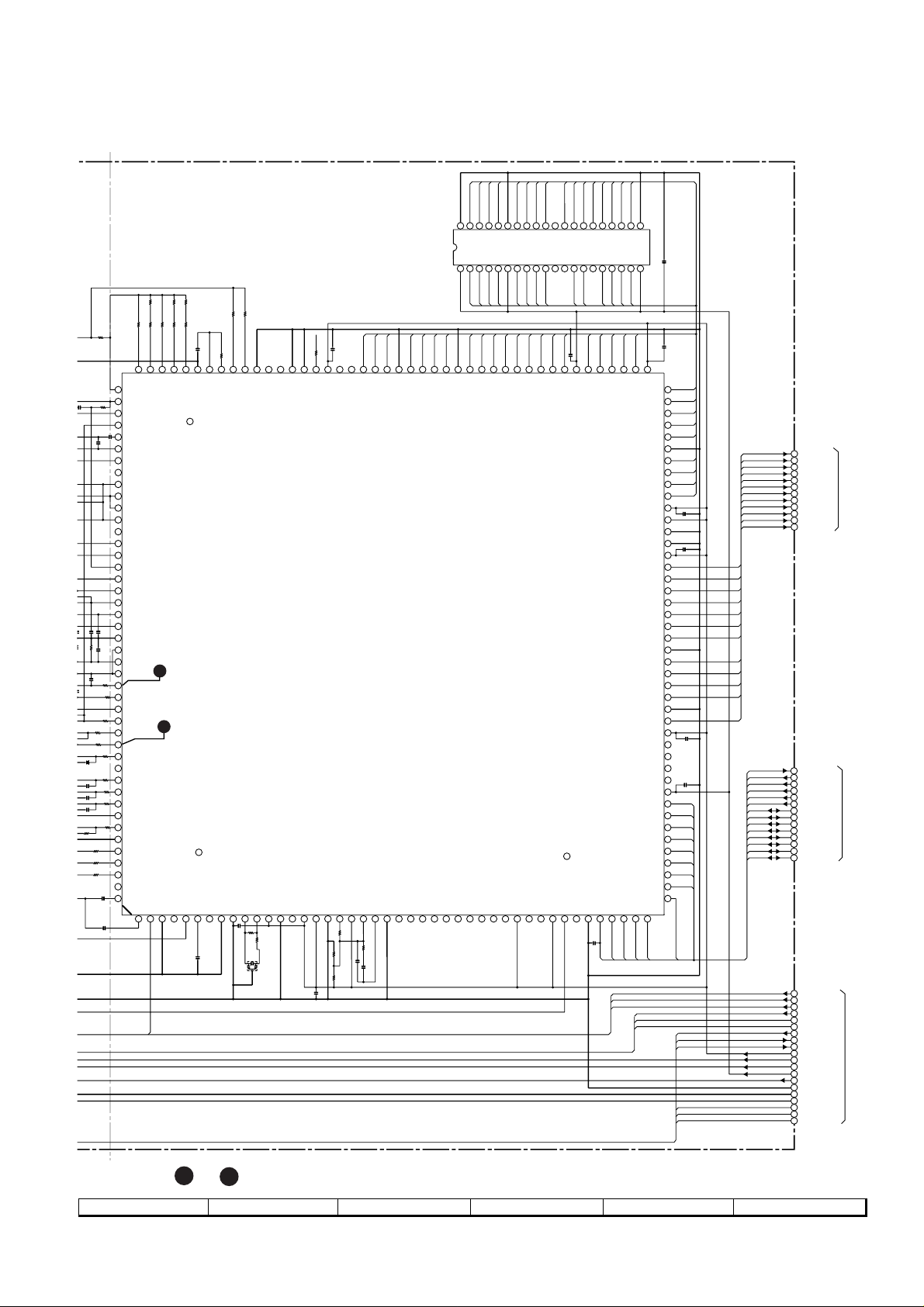
CD-DVD500
7
0
3
OE
LCAS
UCAS
DDAT9
DDAT15
DDAT14
DDAT13
DDAT12
40 39 38 37 36 35 34 33 32 31 30
D14
D15
D16
VSS
IC3702
IX0447AW
R3743
R3739
1.5K
4.7K
18
R3721
15
2.2K
R3724
20
100K
68
C3735
0.01
C3730
0.1
4
5
+B
3
(CH)
C3734
C3728
220P
18K
R3717
C3729
0.0047
R3727
330
R3728
330
R3729
39K
R3730 27K
5
R3731 27K
R3732
C3723
0.1
R3734
R3735
R3736
R3725
R3718
150
R3719
150
R3720
150
C3732
0.1
C3733
560P
10K
10K
10K
10K
1K
0.1
R3738 33K
132 131 130
133
PDON2
LPFO
134
PVREF
135
VCOREF
136
VCOF
137
PVDD
138
RFOn
139
TESM9
140
TEST2
141
RFCD
142
RFDVD
143
AVDD
144
RFCT
145
RFZI
146
TEZI
147
AWIN
148
AVSS
149
FEI
150
TEI
151
LVL
152
RFRP
153
AVSS
154
TESM10
155
0.001
C3731
EXTAD
156
VREF
157
158
FOO
TRO
159
AVDD
160
AWCTL
161
FMO
162
163
DMO
TEBC
164
NC(FEBC)
165
DPDC
166
EQBC
167
ANMON
168
/DFCT
169
VRCK
170
VSS3
171
SCD
172
SCL
173
SCB
174
FGIN
175
176
ASLCN
1234567
R3740 47K
PDOP2
ASLCO
10K
R3745
R3746
100K
R3742 33K
R3744 47K
C3741
129 128 127 126 125 124
PESP
PVSS
PDOP1
PDON1
133
LPFN
2
3
176
DACVSS
DACVDDRODVR
+B
C3742
0.01
PESV
ASLCP
LO
0.1
150K
R3750
R3753
33K
R3748
123 122 121 120 119 118
PPW
CFC2
CFC1
DACVSS
XVSSXIXO
10 11 12 13 14 15
89
0.1
C3744
330K
VSS3
R3754
R3755
TESM8
XVDD
1M
470
FL3701
22.5792MHz
TESM7
TESM0
TESM6
TESM1
C3746
0.1
TESM5
TESM2
10
R3756
117 116 115 114
PLCK
VDD3
16 17 18 19
R3757
+B
4M EDO RAM
+B
0.1
C3747
DDAT13
DDAT14
DDAT15
113 112 111 110 109
NC
NC
BD15
VDD3
BD14
IC3701
TC94A03F
SERVO ECC
VSS3
VPFC
TEST0
VLPFI
VLPFO
20 21 22 23 24 25 26 27 28
1K
R3759
R3758
10K
C3748
1K
R3760
0.01
0.01
C3749
10K
DDAT11
DDAT12
108 107 106 105 104 103 102 101 100
BD11
BD13
BD12
VSS5
VSS3
MON0
MON1
MON2
D1
VCC
123456789
+B
DDAT1
DDAT0
DDAT7
DDAT8
DDAT9
DDAT10
BD9
BD8
BD10
MON3
BD7
VSS3
MON4
MON5
MON6
MON7
29 30 31 32 33 34 35 36 37
DDAT2
DDAT6
BD6
MON8
DDAT3
DDAT8
DDAT11
DDAT10
D10
D11
D12
D13
VSS
D5
D4D3D2
VCC
10 11
DDAT7
DDAT6
DDAT5
DDAT4
DDAT2
DDAT3
DDAT4
DDAT5
99 98 97 96 95 94 93 92 91 90 89
BD5
BD4
BD3
BD2
MON9
VDD3NCNC
+B
ASLCO
+B
+B
+B
DADR8
DADR7
29 28 27 26 25 24 23 22 21
D9
NC
LCAS
UCAS
D8D7D6
NC
NC
WE
12 13 14 15 16 17 18 19 20
WE
DADR0
RAS
+B
WE
LCAS
DDAT0
DDAT1
0.1
C3750
BD1
BD0
/BWE
VDD5
/BCASL
45
/MINT
TEST1
FLGA
FLGB
VSS3
/RST
38 39 40 41 42 43 44
C3751
0.001
DADR6
DADR5
DADR2
DADR1
RAS
UCAS
/BCAS
/MA
/SRV_RST
/MA
TE
LVL
RFRP
/BRAS
/MRD
DADR4
A4A5A6A7A8
A3A2A1A0NCOERAS
DADR3
OE
/MWR
/RD
+B
VSS
/BOE
TESM4
TESM3
/WR
CHOP
DVD_L
MUTE
VCC
VDD3
BA4
VSS5
VDD3
DIGI
VDD5
PDCK
/PDRQ
/PSYC
PD8
PD7
PD6
PD5
VSS3
PD4
PD3
PD2
PD1
VSS5
PD0
VDD3
VMCK
SMCK
VDD5
MD7
MD6
MD5
MD4
MD3
MD2
MD1
MD0
/MCE
BA8
BA7
BA6
BA5
BA3
BA2
BA1
BA0
NC
NC
/SRV_CS
C3753
88
87
86
85
84
83
82
81
80
79
78
77
76
75
74
73
72
71
70
69
68
67
66
65
64
63
62
61
60
59
58
57
56
55
54
53
52
51
50
49
48
47
46
45
C3752
0.1
+B
0.1
DADR8
DADR7
DADR6
DADR5
DADR4
DADR3
DADR2
DADR1
DADR0
C3756
0.1
C3757
0.1
+B
C3759
0.1
C3758
0.1
MD7
MD6
MD5
MD4
MD3
MD2
MD1
MD0
/SRV_INT
IN_SW
LD_RVS
LD_FWD
+B
CAM_SW
DISC1_SW
DVD_FUNC
+B
+B
+B
SDCK_I
/SVAL_I
/SOSO_I
/ERR_I
SD7_I
SD6_I
SD5_I
SD4_I
SD3_I
SD2_I
SD1_I
SD0_I
SDCK_I
/SVAL_I
/SOSO_I
/ERR_I
SD0_I
SD1_I
SD2_I
SD3_I
SD4_I
SD5_I
SD6_I
SD7_I
/SRV_INT
/SRV_CS
/SRV_RST
/WR
+B
/RD
/MA
MD0
MD1
MD2
MD3
MD4
MD5
MD6
MD7
+B
+B
+B
+B
+B
SDCK_I
1
/SVAL_I
2
/SOSO_I
3
4
/ERR_I
5
SD0_I
SD1_I
6
SD2_I
7
8
SD3_I
SD4_I
9
SD5_I
10
11
SD6_I
12
SD7_I
13
/SRV_INT
14
/SRV_CS
15
/SRV_RST
16
/WR
17
/RD
18
/MA
MD0
19
20
MD1
21
MD2
22
MD3
23
MD4
24
MD5
MD6
25
26
MD7
27
TE
28
LVL
RFRP
29
CHOP
30
31
DVD_L
MUTE
32
IN_SW
33
LD_RVS
34
LD_FWD
35
D_3.3V
36
37
A_3.3V
38
A_5V
D_5V
39
+B
40
AT_8V
41
D_GND
42
M_GND
43
A_GND
44
CAM_SW
45
DISC1_SW
DVD_FUNC
46
P28 1-C
TO DVD SERVO PWB-C (2/3)
P28 1-D
TO DVD SERVO PWB-C (2/3)
P28 1-H, 1-E
TO DVD SERVO PWB-C (2/3)
• The numbers 2 to 6 are waveform numbers shown in page 58.
7
8 9 10 11 12
Figure 27 SCHEMATIC DIAGRAM (2/18)
– 27 –
Page 28
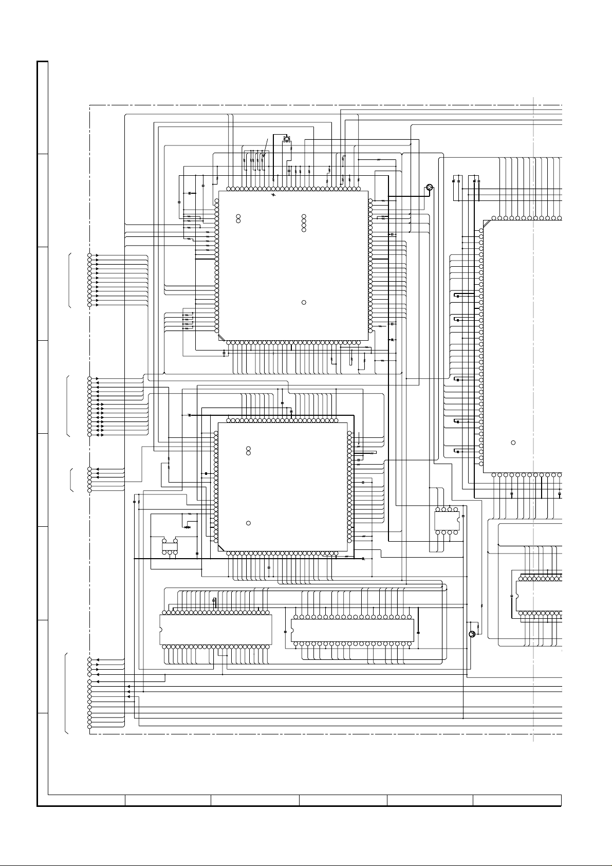
CD-DVD500
1
0
VSSO
VSSO
B
/SVAL O
1
6
4
S
A
B
SDCK_I
1
/SVAL_I
2
/SOSO_I
3
/ERR_I
4
SD0_I
5
SD1_I
6
SD2_I
7
SD3_I
P27 12-C
8
SD4_I
9
SD5_I
C
D
E
F
G
10
SD6_I
11
TO DVD SERVO PWB-C (2/3)
SD7_I
12
13
/SRV_INT
14
/SRV_CS
15
/SRV_RS
16
/WR
17
/RD
18
/MA
MD0
19
MD1
20
P27 12-F
MD2
21
MD3
22
MD4
23
MD5
24
TO DVD SERVO PWB-C (2/3)
MD6
25
26
MD7
TE
27
LVL
28
RFRP
29
CHOP
30
DVD_L
31
P27 12-H
MUTE
32
TO DVD SERVO PWB-C (2/3)
IN_SW
33
LD_RVS
34
LD_FWD
35
D_3.3V
36
A_3.3V
37
A_5V
38
D_5V
39
AT_8V
40
P27 12-H
D_GND
41
M_GND
42
A_GND
43
TO DVD SERVO PWB-C (2/3)
CAM_SW
44
DVD_FANC
45
DISC1_SW
46
RFRP
DVD_L
MUTE
IN_SW
LD_RVS
LD_FWD
CAM_SW
DVD_FANC
DISC1_SW
FL3501
R3518
20MHz
MUTE
WAIT
R3513
R3510
R3511
1
+B
1.5V
1.5V
0.3V
3.0V
4.7K
0.1
C3508
91
MUTE
DVD_L
92
AVCC
93
VREF
94
KEY1
95
KEY2
96
KEY3
97
R3508 10
LVL
98
R3509 10
TE
99
EJ_SW
100
4.7K
RFRP
101
R3512 10
RESERVE(SRV)
102
AVSS
103
10K
VSS
104
STANBY
105
TRAY_ACK
106
WOBBLE
107
S1_H
108
VMUTE
109
ADAC_DA
110
ADAC_CK
111
ADAC_L
112
MD_0
113
MD_1
114
MD_2
115
CAS
116
R3502
SRV_CS
117
10K
RAS
118
R3503
AV_CS
119
10K
FROM_CS
120
VCC A0A1A2A3A4A5A6A7A8A9
1 2 3 4 5 6 7 8 9
C3501
0.1
A0A1A2A3A4A5A6A7A8A9A10
+B
75 74 73 72 71 70 69 68 67 66 65 64 63 62 61 60 59 58 57 56 55 54 53 52 51
NC
VSS
+B
76
77
BUF5INBO
78
BUF5ONAO
79
BUF5INAO
80
GPON3O
81
GPON2O
82
GPON1O
83
GPON0O
84
0.01
C3523
VSS
85
VDD1
86
LIN1O
87
LIN2O
88
BUFONCO
89
BUFINCO
90
BUFONBO
91
BUFINBO
92
BUFONAO
93
BUFINAO
94
TEST0
95
TEST1
96
TEST2
97
NC
98
MRST
99
100
HADR0
VDD1
1 2 3 4 5 6 7 8 9
A0A1A2A3A4A5A6A7D8D9D10
+B
C3517
0.01
0.2V
0.2V
1.6V
0.2V
1.5V
0.3V
0.2V
0.3V
3.3V
33 32 31 30 29 28 27 26 25
D2D9D1D8D0
VDD
/WE
/RP
VPP
NC
10 11 12 13 14 15
0V
0V
0V
3.3V
A18
/WP
RY/BY
16 17 18 19 20 21 22 23 24
0V
3.3V
3.3V
A8A9A10
NC
0V
C3510
0.1
C3511
0.1
R3505
3.3K
R3506
KEY3
LVL
TE
RFRP
SDCK_I
/SVAL_I
/SOSO_I
/ERR_I
SD0_I
SD1_I
SD2_I
SD3_I
SD4_I
SD5_I
SD6_I
SD7_I
/SRV_INT
/SRV_CS
/WR
/RD
/MA
MD0
MD1
MD2
MD3
MD4
MD5
MD6
MD7
TE
LVL
C3524
0.0047
+B
3.3K
R3507
3.3K
R3530
10K
ADAC_DA
ADAC_CK
ADAC_L
CAS
/SRV_CS
RAS
AVCS
FRCS
R3564
5.6K
R3565
10K
+B
47K
R3523
D3501
DAP202K
4
5
1 2 3
IC3503
PST9129N
RESET
0V0V0V
0V
3.3V
0V
48 47 46 45 44 43 42 41 40 39 38 37 36 35 34
A16
D15D7D14D6D13D5D12D4D11D3D10
VSS
/BYTE
IC3501 IX1689GE
FLASH ROM
A12
A13
A14
A15
1 2 3 4 5 6 7 8 9
+B
3.3V
0.2V
0.3V
0.4V
+B
+B
R3501
+B
3.0V
1K
R3504
10K
C3522
47/6.3
R3515
150K
C3512
A11
2.8V
+B
1K
DVD_L
R3517
1K
/AS
1K
LCAS
R3514
/RD
/WR
R3520
FIP_CS
R3516 10K
R3519 1K
80 79 78 77 76 75 74 73 72 71 70 69 68 67 66 65 64 63 62 61 90 89 88 87 86 85 84 83 82 81
/AS
/RD
VCC
/LWR
LCAS
/HWR
S/E_CS
AMUTE2
91
MODE_SW
WAIT
92
DVD MICROCOMPUTER
VSS
10 11 12 13 14 15 16 17 18 19 20 21 22 23 24 25 26 27 28 29 30
MD5
MD4
MD3
MD2
MD1
MD0
NC
5VBUSN0O
5VBUSN1O
5VBUSN2O
5VBUSN3O
5VBUSN4O
5VBUSN5O
5VBUSN6O
VDD1
76
BUF5ONBO
77
IC3508
IX1761GE
TRACK
BUFFER INTERFACE
100
VSS
HADR7
HADR6
HADR5
HADR4
HADR3
HADR2
HADR1
VSS
10 11 12 13 14 15 16 17 18 19 20 21 22 23 24 25
C3525
1.6V
0.3V
0.9V
0.2V
0.2V
0.2V
0V
A0
/CE
/OE
VSS
A17
0V
A1A2A3A4A5A6A7
0.3V
0.1V
3.0V
0.3V
0.3V
0.3V
0.3V
R3522
10
R3528
10K
R3524 10K
C3506 0.1
R3525 10K
NMI
VSS
VCC
XTAL
/STBY
EXTAL
/RESET
/WDGOVF
HGA_CS
60
59
VSS
UART-CTL
58
SUB/EEP CLK
57
IC3504
IX1687GE
31
SRV_INT
A10
A11
A12
A13
A14
A15
VSS
A11
A12
A13
A14
A15
0.01
C3521
MD7
MD6
0.01
SD3_I
SD2_I
SD1_I
SD0_I
C3520
VSS
VSS
VDD1
VDD2
PDIN0O
PDIN1O
PDIN2O
5VBUSN7O
VDD1
0.01
+B
C3515
0.01
PDIN3O
HDAT7
HDAT6
HDAT5
HDAT4
HDAT3
HDAT2
HDAT1
HDAT0
D11
D12
D13
D14
D15
D14
D15
40 39 38 37 36 35 34 33 32 31 30
VSS
DQ15
DQ16
DQ2
DQ1
VCC
1 2 3 4 5 6 7 8 9
+B
D0D1D2D3D4D5D6
10K
LD-FWD
G_RESET
A16
A17
A16
A17
+B
SD4_I
PDIN4O
PDIN5O
HWR
HRD
/RD
/WR
D12
D13
DQ14
DQ13
DQ3
LD-RVS
A18
A18
SD5_I
PDIN6O
HAS
DQ4
10K
R3532
4.7K
R3531
CHOP
LD_SW
A19
VSS
10K
R3533
A19
SD7_I
SD6_I
PDIN7O
PDIN8O
DVDREQ
PDCKO
PDRQO
PSYCO
PDON8O
PDON7O
PDON6O
PDON5O
PDON4O
PDON3O
PDON2O
PDON1O
PDON0O
HCS2
HCS1
HGA_CS
/SRV_CS
D11
VSS
DQ12
DQ5
VCC
/MA
R3534
10K
R3535
/MA
Z_RESET
SUB/EEP Din
SUB/EEP Dout
HGA_INT
A20
R3538
A20
HGA_INT
/ERR_I
VSS
VDD2
PSYCI
PDRQI
PDCKI
VDD2
VSS
VDD1
VSS
VSS
HINT
HWAIT
VDD1
VSS
R3560
10K
D9
D10
DQ10
DQ11
DQ7
DQ6
10K
EECS
10K
R3537
Z_STNBY
PLAY_MODE
UART-RXD
UART-TXD
H/P CTL
TRAY_REQ
10K
50
49
48
47
46
45
44
43
42
41
40
39
38
37
36
35
34
33
32
31
30
29
28
27
26
D8
DQ9
10 11
D7
R3543 10K
+B+B+B
HGA_CS
4.7K
R3540
R3544
4.7K
60
IN_SW
EEP-CS
59
R3546
58
100K
57
56
UART-RXD
R3547
55
1K
54
53
C3504
VCC
52
0.1
51
50
49
48
47
46
45
44
43
42
41
40
39
38
37
36
35
34
R3554
33
10K
32
31
1K
R3556
1K
R3545
1K
/SRV_INT
/SOSO_I
/SVAL_I
SDCK_I
0.01
SDCK_O
/SVAL_O
/SOSO_O
/ERR_O
SD7_O
SD6_O
SD5_O
SD4_O
SD3_O
SD2_O
SD1_O
SD0_O
HGA_INT
A9
CAS
A8
A7
OE
UCAS
IC3502
A0NCRAS WENCNCDQ8
/WR
RASA1A2A3A4 A5
C3503
+B
A1A2A3
D15
D14
D13
D12
D11
D10
D9
D8
D7
D6
D5
D4
D3
D2
D1
D0
+B
A6A7A8
D15
D14
D13
D12
VSS
D11
D10
D9
D8
D7
D6
D5
D4
VSS
D3
D2
D1
D0
VCC
R/C
AV_INT
STBY_REQ
R3541
AV_INT
+B
100
R3568
R3566 10K
C3528
R3569
100
C3527
0.01
R3581
10K
C3526
47/6.3
+B
LCAS
29 28 27 26 25 24 23 22 21
NC
LCAS
12 13 14 15 16 17 18 19 20
0.1
C3502
100/6.3
A4A5A6
KRC104 S
S/E_CK
S/E_DI
S/E_DO
IC3507
BR93L66F
IC3502
IX0448
DRAM
VSS
C3516
VCC
Q3503
3
2
1
EEPROM
4M
0.01
C3601
100/6.3
D15
D14
D13
D12
D11
D10
0.1
C3605
D9
D8
0.1
C3606
D7
D6
D5
D4
D3
D2
D1
D0
C3607
A4
0.1
A3
A2
A1
/WR
AVCS
C3608
0.1
/RD
AV_INT
0.1
C3609
WAIT
EECS
S/E_CK
4 3 2 1
CS
VCC
CLK
DIN
OCNT
GND
5 6 7 8
S/E_DO
S/E_DI
+B
+B
+B
+B
C3602
+B
+B
C3603
100/6.3
0.1
+B
+B
+B
+B
C3519
0.01
NC NC
R3557
2.2K
R3558
4.7K
Q3502
KTA1504 Y
VPP_CTL
+B
SD6_O
SD7_O
C3604
0.1
+B
+B
IDLE
159160 158 157 156 155 154 153 152 151 150 149
HORD
1
HWID
2
DVDDAT7
DVDDAT6
DVDDAT5
VDDP
3
HTYPE
4
HD-15
5
HD-14
6
HD-13
7
HD-12
8
HD-11
9
GNDP
10
HD-10
11
VDDC
12
HD-9
13
GNDC
14
HD-8
15
VDDP
16
HD-7
17
HD-6
18
VDD_LVL_SHFT
19
HD-5
20
HD-4
21
HD-3
22
HD-2
23
HD-1
24
HD-0
25
VDDP
26
HA-3
27
HA-2
28
HA-1
29
HA-0
30
HWR
31
HCS
32
33
VDDC
HRD
34
GNDC
35
HRDY
36
37
38
39
40
+B
41
HIRQ
VDDP
HACK
GNDP
VDDP
RAMADD5
RAMADD3
41
42 43 44 45 46 47 48 49 50 51 52
+B
C3610
0.1
RAMA4
RAMA3
RAMA5
+B
C3640
0.1
SD1_O
SD2_O
SD3_O
SD4_O
SD5_O
DVDDAT4
DVDDAT3
DVDDAT2
DVDDAT1
DVDDAT0
RAMADD4
GNDP
RAMADD7
RAMADD1
RAMADD6
RAMADD2
RAMA2
RAMA6
RAMA1
RAMA7
RAMD13
RAMD14
RAMD15
50 49 48 47 46 45 44 43 42 4
I/O15
I/O14
I/O13
I/O12
VSSO
VSSO
VSSO
I/O3
I/O2
I/O1
I/O0
VCC
1 2 3 4 5 6 7 8 9
+B
RAMD0
RAMD1
RAMD2
16M
SD0_O
DVDREQ
DVDREQ
RAMADD0
C36
RAMA0
RAMD12
I/O11
VCCO
VCCO
I/O4
RAMD3
IC3
IX04
SDCK_O
DVDSTRB
DVDVALID
VDDP
RAMADD8
0.1
RAMA8
RAMD10
RAMD11
I/O10
I/O5
1
RAMD4
RAMD5
+
H
• NOTES ON SCHEMATIC DIAGRAM can be found on page 56.
1
23456
Figure 28 SCHEMATIC DIAGRAM (3/18)
– 28 –
Page 29
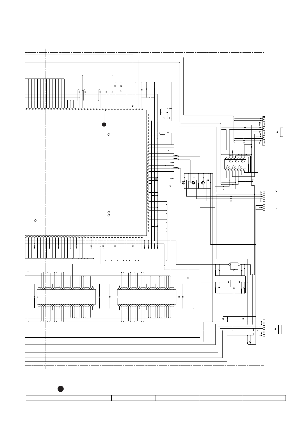
CD-DVD500
IDLE
DVD SERVO PWB-C (2/3)
SD7_O
B+B
15960 158 157 156 155 154 153 152 151 150 149 148 147 146 145 144 143 142 141 140 139 138 137 136 135 134 133 132 131 130 129 128 127 126 125 124 123 122 121
D
D
DVDDAT7
DVDDAT6
DVDDAT5
DVDDAT4
DVDDAT3
DVDDAT2
DVDDAT1
RAMADD4
RAMADD7
RAMADD1
RAMADD6
RAMADD2
VDDP
RAMA2
RAMA6
RAMA1
RAMA7
RAMD13
RAMD14
RAMD15
50 49 48 47 46 45 44 43 42 41
I/O15
I/O14
I/O13
VSSO
VSSO
VSSO
I/O2
I/O1
I/O0
VCC
1 2 3 4 5 6 7 8 9
+B
RAMD0
RAMD1
RAMD2
DVDDAT0
GNDP
P
PE
5
4
3
2
1
P
0
C
C
P
_LVL_SHFT
P
C
C
Y
41
P
K
P
RAMADD5
RAMADD3
1
42 43 44 45 46 47 48 49 50 51 52 53 54 55 56 57 58 59 60 61 62 63 64 65 66 67 68 69 70 71 72 73 74 75 76 77 78 79 80
C3610
0.1
RAMA4
RAMA3
RAMA5
+B
C3640
0.1
SDCK_O
/SVAL_O
DVDREQ
/SOSO_O
DVDSOS
DVDERR
DVDREQ
DVDSTRB
DVDVALID
RAMADD9
RAMADD10
VDDP
RAMADD8
RAMADD0
C3611
0.1
RAMA0
RAMA10
RAMA8
RAMD9
RAMD10
RAMD11
RAMD12
40 39 38 37 36 35 34 33 32 31 30
I/O9
I/O8
I/O12
I/O11
I/O10
VSSO
VCCO
VCCO
VSSO
I/O7
I/O6
I/O5
I/O4
I/O3
10
11 12 13 14 15 16 17 18 19 20 21
RAMD3
RAMD4
RAMD5
RAMD6
IC3602
IX0449AW
16M SDRAM
+B
/EER_O
RAMA9
RAMD8
+B
VCCO
RAMD7
SD0_O
SD1_O
SD2_O
SD3_O
SD4_O
SD5_O
SD6_O
ABCLK
220
R3621
0.1
C3635
GPSI
VDDP
VDDC
GNDP
GPSO
GNDC
ABCLK
IC3601
IX1720GE
DVD DECORDER
RAMCAS
RAMRAS
RAMCS1
VDDP
RAMCS0
GNDP
RAMADD11
C3612
0.1
RAMA11
RAMCS1
RAMRAS
RAMCS0
RAMA7
RAMA8
RAMA9
RAMDQM
A9A8A7A6A5
NC
NC
CLK
CKE
DOMU
A10(+)
A11(BS)
CS
RAS
CAS WEDOML
VCCO
RAMDQM
RAMWE
RAMCAS
RAMCS0
RAMRAS
RAMA11
RAMA10
22 23 24 25
RAMA0
0.1
C3634
+B
ALRCLK
RAMWE
C3613
0.1
RAMCAS
RAMWE
RAMA5
RAMA6
RAMA1
RAMA2
AOUT-2
VDDC
RAMA4
26 27 28 29
A4
VSS
RAMA3
C3633
AOUT-1
RAMDQM
RAMDQM
VCC A3A2A1A0
0.1
VDDP
AOUT-0
PCLK
GNDP
C3614
100
R3670
1
0.1
PCLK
C3641
R3616
GPIO
VDDP
0.1
390
S/PDIF
120
82
81
RAMDAT8
RAMD8
AMCLK
C3632
150
R3615
AMCLK
VDDP-A2
GNDP-A2
TESTMODE
GCLK
RAMDAT3
RAMDAT12
GNDP
RAMDAT9
VDDP
RAMDAT7
C3615
0.1
RAMD7
+B
50 49 48 47 46 45 44 43 42 41 39 40
0.1
C3643
C3631
0.1
47/6.3
L3602
47µH
100mA
FB3606
VDDP
GNDP
RESET
VCLKx2
SCNENBL
VDD_LVL_SHFT
VDDP
RAMDAT5
RAMDAT10
RAMDAT6
GNDC
C3616
0.1
RAMD9
RAMD6
RAMD10
RAMD5
RAMD12
RAMD13
RAMD14
RAMD15
I/O12
I/O13
I/O14
I/O15
VSSO
VSSO
VCCO
VCC
I/O0
I/O1
I/O2
I/O3
VSSO
VCCO
1 2 3 4 5 6 7 8 9
RAMD0
RAMD1
RAMD2
RAMD3
0.1
C3629
C3630
100/6.3
+B
FB3605
100mA
120
VDDA
GNDA
STNBY
XO
119
PLLCFG-0
118
GCLK1
117
VDDC
116
PLLCFG-1
115
GNDC
114
AIN
113
ICEMODE
112
VREF
111
GND-DACS
110
GND-DACP
109
RSET
108
GND-DACB
107
C/B/U
106
Y/R/V
105
VDD-DAC
104
CVBS/C
103
CVBS/G/Y
102
GND-DACD
101
COSYNC
100
VDDP
99
98
GNDP
97
FI
96
HSYNC
95
VDDP
94
VSYNC
93
VCLK
92
RAMDAT0
91
RAMDAT15
90
VDDP
89
RAMDAT1
88
RAMDAT14
87
GNDP
86
RAMDAT2
85
RAMDAT13
84
VDDP
83
82
81
GNDP
RAMDAT4
RAMDAT11
+B
C3617
100/6.3
RAMD11
RAMD4
RAMD8
RAMD9
RAMD10
RAMD11
38 37 36 35 34 33 32 31 30 29 28
I/O8
I/O9
I/O10
I/O11
VSSO
VCCO
I/O4
I/O5
I/O6
I/O7
VCCO
VSSO
10 11 12
13 14 15 16 17 18 19 20 21 22 23
RAMD4
RAMD5
RAMD6
RAMD7
IC3603
IX0449AW
16M SDRAM
+B
0.1
C3618
RAMDQM
NC
DOMU
DOMLWECAS
RAMDQM
RAMWE
C3628
+B
R3603
C3623
+B
C3622
RDMD15
RDMD14
RDMD13
C3621
RDMD12
+B
C3620
100/6.3
0.1
C3619
FB3601
100mA
NC
CLK
CKE
RAS CSA11(BS)
RAMCAS
RAMCS1
RAMRAS
47/6.3
10P(CH)
R3613
150
R3602
10K
R3604
390
56
0.1
0.1
RDMD0
RDMD1
RDMD2
0.1
RDMD3
RAMA9
A9
A10(+)A0A1A2A3
RAMA11
C3627
680K
R3612
FB3604
100mA
C3625
C3624
L3601
RAMA7
RAMA8
RAMA10
RAMA0
X3601
0.1
47/6.3
47µH
RAMA6
27 26
24 25
RAMA1
27MHz
RAMA4
RAMA5
A4A5A6A7A8
RAMA2
RAMA3
C3626
10P(CH)
R3607
56
R3610
56
Q3205
KTA1504 Y
+B
VSS
VCC
R3608
C3644
+B+B
CP3202
LD+
1
8
9
R3214
1.8K
IC3201
+B
C3673
+B
C3667
C3672
0.01
R3205
10K
R3212
1.8K
GND
+B
C3674
47/6.3
47/6.3
C3206 0.1
+B
+B
+B
+B
0.1
C3207
0.001
C3671
10K
R3206
100/6.3
LD–
2
D_GND
3
DVD_STB
4
UART RX
5
DVD_BUSY
6
DVD_DO
7
DVD_DI
8
DVD_CLK
9
TUN_FNC
10
CLAMP SW
11
CD/D1_SW
12
47
SPDIF_O
48
D_5V
CVBS/G/Y
49
50
Y/R/V
51
C/B/U
53
A_GND
+B
54
V_8V
D_GND
55
+B
CP3201
A_5V
1
D_5V
2
M_GND
3
A_GND
4
D_GND
5
M_8V
6
V_8V
7
+B
P33 8-H
CNS703
FROM DISPLAY PWB
P43 11-H
PWB-C (3/3)
TO DVD SERVO
CNS405
P35 7-E
FROM AMP. B PWB
LD_FWD
LD_RVS
R3215
100
R3211
470
14
13 12 11 10
VCC
1 2 3 4 5 6 7
R3213
470
74HC07AF
BUFFER AMP.
R3661 10
R3662 10
R3663 10
IC3662
IX0472AW
3
2
C3666
47/6.3
0.1
3 1
2
47/6.3
C3665
0.1
C3669
0.01
C3668
0.01
+B
R3204 100
R3228 100
R3203 100
R3208 100
R3209 100
1
UART-RXD
KEY3
FIP_CS
R3216
+B
C3205
C3204 0.1
47/6.3
R3207 10K
R3210 10K
+B
+B
22K
S/E_CK
S/E_DI
S/E_DO
56
R3227
680
R3226
C3201 0.1
Q3203
KTA1504 Y
Q3202
KTA1504 Y
+B
680
680
R3225
0.1
C3203
+B
VOLTAGE REGULATOR
0.1
C3662
0.1
C3661
+B
IX0445AW
VOLTAGE
REGULATOR
C3670
100/6.3
+B
+B
D1.8V
C3664
C3663
IC3661
+B
+B
100mA
FB3603
+B
0.1
C3646
+B
+B
100/6.3
+B
• The number 1 are waveform number shown in page 58.
7
8 9 10 11 12
Figure 29 SCHEMATIC DIAGRAM (4/18)
+B
– 29 –
Page 30
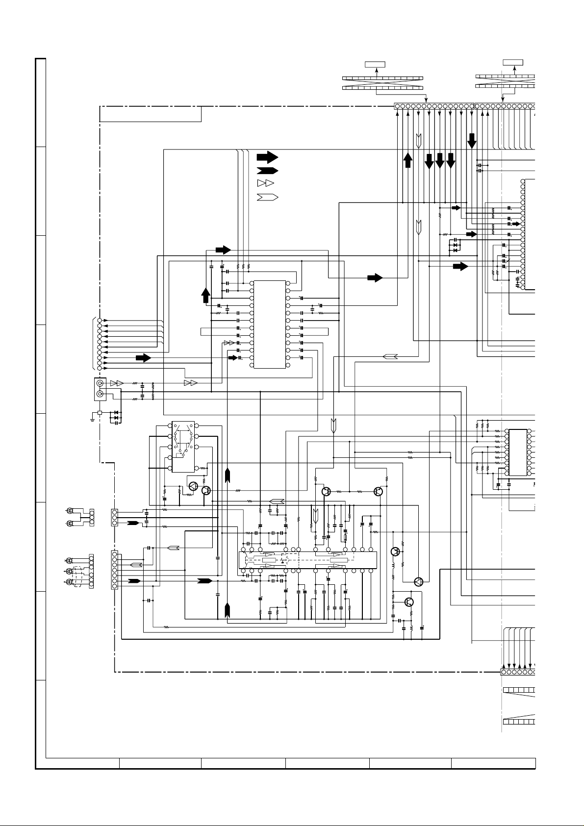
CD-DVD500
S
S
S
E
S
S
R
D
D
1
T
B
4
E
L
2
T
D
A
B
C
TO
TUNER PWB
P41 11-H
D
E
F
G
JK601
VIDEO/AUX IN
TAPE 1
PLAYBACK HEAD
L-CH R-CH
ERASE HEAD
R-CH
L-CH
TAPE 2
RECORD/
PLAYBACK HEAD
L-CH
R-CH
CHASSIS
1
2
3
1
2
3
4
5
6
MAIN PWB-A (1/2)
DO
1
CE
2
DI
3
CLK
4
TUN_SM
5
D_GND
6
A_+10V
+B
7
TUN_L
8
A_GND
9
TUN_R
10
(CH)
390P
C629
R625
4.7K
R627
39K
R628
39K
4.7K
(CH)
390P
R626
C630
D601
DS1SS133
T1_R
A_GND
T1_L
M_GND
ERASE
T2_R2
A_GND
T2_R1
T2_L1
T2_L2
C600
0.022
CNP101
1
2
3
CNP102
1
2
3
4
5
6
7
D602
DS1SS133
HEAD SELECTOR
C102
560P
C101
560P
C106
180P(CH)
C105
180P
R101
1K
R113
15K
R102
1
2
3
4
5
KRC104 M
R103
C103
10/16
1K
+B
IC102
BA3126N
Q101
2
1
2.2K
2.2K
R106
R107
1K
9
8
7
R105
100
6
3
Q102
KTC3199 GR
C602
0.022
R110
C603
100P
(CH)
33K
C108
R605
3.9K
560P
C601
100/16
C626
100P(CH)
100P(CH)
C623
10/50
C609
0.0027
C107
C613
1/50
C617
560P
1/50
C111
180P
C604
C605
(CH)
R602
0.1
R104
L
1K
R601
C607
0.1
C611
1/50
C615
1/50
C619
1/50
+B
5.6K
R
R118
C112
180P(CH)
24
123
R117
1K
1K
R114
15K
1K
CLK DICE
R603
1
2
3
4
5
6
7
8
9
10
11
C114
180P
(CH)
23
C113
180P
(CH)
FM SIGNAL
PLAYBACK SIGNAL
VIDEO IN SIGNAL
RECORD SIGNAL
IC601
LC75341
AUDIO PROCESSOR
1K
IC601
LC75341
DI
CE
VSS
LOUT
LBASS
LTRE
LIN
LSEL0
L4
L3
L2
TUNER
L1
56
R120
C124
C116
100/25
22
–
+
Hich=T1
+
–
C115
100/25
56
R119
C123
+B
24
CLK
23
VDD
C625
22/50
22
VREF
C606
21
ROUT
RBASS
RSEL0
AUX
DECK
DVD
0.0015
C118
0.033
R122
100K
112K
R121
100K
C117
0.033
0.0015
PLAYBACK AND RECORD/
0.1
C608
0.1
20
C610
0.0027
19
RTRE
C612
18
RIN
1/50
C614
1/50
17
C616
1/50
16
R4
C618
1/50
15
R3
C620
1/50
14
R2
R1
13 12
R
6.8K
R132
68K
R134
5.6K
R126
1/50
C122
5.6K
R136
C120
560P
R124
R138
3.9K
19
20
21
IC101
AN7345K
112K
4
6
5
R123
3.9K
C119
560P
R137
1/50
C121
C127
0.022
C128
3.3/50
5.6K
R125
6.8K
R131
R135
IC101
AN7345K
PLAYBACK AMP.
6.8K
18
7
6.8K
5.6K
FFC602
C624
10/50
R606
3.9K
82K
R156
KTC3199 GR
0V
0V
C132
270P(CH)
17
C131
270P(CH)
DOLBY PWB
15
1
Q122
0.7V
R154
10K
100
R142
C140
1.5K
R140
C136
0.022
C134
22/25
–
56K
+
Hich=CHROME
+
56K
–
8
C133
22/25
100
R141
C135
0.022
1.5K
R139
TO
P37 12-D
+B
0.0033
C142
16
15
10
9
C141
47/25
R145
10K
C139
0.0033
R153
10K
Q121
KTC3199 GR
10K
R146
47/25
C145
14
RIPPLE
Nor/CrO2
ALC
ALC
11
CNP502
0.7V
22/25
13
12
R158
Vcc
GND
220
CNP602
C146
220/10
0V
R157
0V
82K
1 2 3 4 5 7 8 9
L_OUT
R_OUT
A_GND
A_GND
R109
270K
R108
+B
270K
+B
47K
R162
11.7V
11.6V
Q124
2SA1015 GR
0V
4.7K
R164
L103
100µH
0V
82
R160
11.6V
0V
47K
R167
0V
0V
22K
R166
C150
0.0082(PP)
C154
0.047(ML)
C151
0.039(ML)
R_F
KRC104 M
Q128
KTC3203 Y
4.7
R168
L104
330µH
1
15
6
A_GND
0V
Q126
C152
L_F
47/25
SW
A_GND
270K
R645
11 12 13 15
10
A_GND
CENTER
R646
270K
T_BIAS
T1/T2
REC/PLAY
R_S
A_GND
C187
0.022
DS1SS133
D183
DS1SS133
+B
12
14
L_S
A_GND
C190
C189
D184
FAN_CTL
+B
R178
DD_RST
1
12 11
10
D_5V
D_GND
A_10V
+B
+B
0.022
0.022
+B
R177
10K
10K
R190 100
R191 100
R192 1K
–11DB_ATT
10K
R180
10K
R179
R193 100
R195 100
R196
CNP503
9 8 7 6 4 3 2
5
DIO
CK
LOCK
DDAC
DDCE
DDLAT
DD_ACK
DD_DIO
DD_CLK
DD_LOCK
DD_CS
DD_LP
1
2
3
4
C633
R665
10K
R667 10K
R668 10K
C654 22/50
R632
+B
R176
R194 1K
NC
+B
4.7K
22/50
R666
C646
10K
22/50
C645 22/50
C634 22/50
C653
22/50
C631
22/50
10K
10K
R631
+B
INPUT/OU
R189
10K
100
10
11
12
13
14
15
16
17
18
C185
47/16
DD_CLK
1 3 4 5 76 2
10
11
12
13
14
C632
15
22/50
16
C196
17
0.0082
18
19
C197
0.015
20
21
0.33
C194
6-CH EL
IC181
BU209
EXPAN
Q5
Q6
Q7
Q8
Q9
Q10
LCK
Q11
CLOCK
__
OE
DATA
VDD
VSS
C184
0.022
+B
DD_LP
DD_ACK
DD_DIO
5
6
7
8
9
M62
DOL
P37
RESET
DD_STATUS
DD_RST
AVDD
SWIN
S_GN
SR_IN
SL_IN
C_GN
C_IN
GND_
R_IN
GND
L_IN
BYPA
BYPA
L_TR
L_BA
L_BA
L_BA
IC
VO
R
9
Q4
R
8
Q3
R
Q2
7
R
6
Q1
R
Q0
5
4
3
2
1
C109
47/16
R133
DD_LOCK
DD_CS
A_13V
3.9K
DD_STATUS
H
• NOTES ON SCHEMATIC DIAGRAM can be found on page 56.
1
23456
Figure 30 SCHEMATIC DIAGRAM (5/18)
1
36
– 30 –
Page 31

D
GND
_
10K
R180
0
0220
022
12 11
_
D_5V
A_10V
+B
.
.
3
+B
R177
10K
R190 100
R191 100
R192 1K
CTL
11DB_ATT
D_RST
10K
10K
R179
+B
R665
R667 10K
R668 10K
C654 22/50
+B
R193 100
R194 1K
NC
R195 100
R196
CNP503
DOLBY PWB
9 8 7 6 4 3 2
DIO
CK
LOCK
DDAC
DDCE
DDLAT
RESET
DD_ACK
DD_DIO
DD_CLK
DD_LOCK
DD_CS
DD_LP
DD_RST
1
2
3
4
C633
AVDD
5
22/50
10K
R666
10K
C645 22/50
C634 22/50
C653
22/50
10K
R632
R189
10K
R176
+B
4.7K
SWIN
6
C646
S_GND
7
22/50
SR_IN
8
SL_IN
9
C_GND
10
C_IN
11
GND_R
12
R_IN
13
GND
14
C632
L_IN
15
22/50
BYPASS_R
16
C196
BYPASS_L
17
0.0082
C631
L_TRE
18
22/50
L_BASS3
19
C197
0.015
L_BASS2
20
10K
21
R631
0.33
C194
+B
M62446FP
6-CH ELECTRONIC
VOLUME
IC181
BU2092F
INPUT/OUTPUT
EXPANDER
100
10
Q5
Q4
11
Q6
Q3
12
Q7
Q2
13
Q8
Q1
14
Q9
Q0
15
Q10
LCK
16
Q11
CLOCK
__
OE
17
DATA
18
VDD
VSS
C185
47/16
C184
0.022
+B
DD_LP
DD_ACK
DD_DIO
DD_CS
DD_CLK
1 3 4 5 7 8
1
TO
P37 12-B
1 5 10
A_13V
+B
DD_STATUS
IC602
R188 1K
9
R187 1K
8
R186 100
7
R185 100
6
R184 100
5
4
3
2
1
C109
47/16
C183
3.9K
R133
DD_STATUS
DD_LOCK
TUN_SM
6 2
CNP607
R644
10
DVDD
DATA
LATCH
D_GND
A_GND
SW_OUT
SR_OUT
SL_OUT
C_OUT
R_OUT
L_OUT
AVSS
R_TRE
R_BASS3
R_BASS2
R_BASS1L_BASS1
SW-MUTE
RLY2/6
SW-SPRLY
S-SPRLY
C-SPRLY
R183 1K
R182 1K
R181 1K
C182
100P(CH)
100P(CH)
Q103
KTC3199 GR
+B
HP_SW/MIC_IN
A_10V
10 11 12 13 15 16 17 18 19 20 21 22 23 24 25 26 27 28 29 30 31 32 33 34 35 3614
9
12
FFC607
1
42
CLK
41
40
CL1
CL2
CR1
CR2
C195
(CH)
100P
C181
KARA_LAT
–15V
C644
39
C188
38
0.022
37
36
35
34
33
32
31
30
29
28
27
26
25
24
23
22
0.33
LCK2
CLK
DI
R604
VOL_LAT
0.022
10K
CLK
R643 1K
C638
22/50
C640
22/50
C639
22/50
C637
22/50
C636
22/50
C635
22/50
C655
3.3/50
C656
Q601 KTA1271 Y
3.3/50
C199
0.0082
C198
0.015
ZD601 DZ7.5BSC
C649
47/25
DZ7.5BSC
+B
D_GND
R175 10K
R174 10K
R173 4.7K
R172 4.7K
R171 4.7K
+B
+B
-20DB_ATT
S_MUTE
SWD_+5V
CENTER
VOL_LAT
DI
R642 1K
R641 1K
C643 100P(CH)
C642 100P(CH)
C641 100P(CH)
D186
DS1SS133
R63710K
R63810K
R63510K
R63610K
C650
47/25
Q602
KTC3203 Y
ZD602
+B
+B
5V
AT_8V
SPEANA
SW
D185
DS1SS133
RS
LS
R64010K
R63910K
1K
R634
C648
47/25
1K
R633
C647
47/25
+B
CE
CLKDIDO
R-CH
L-CH
CNP404
TO
AMP B PWB
P35 7-H
SPAN
DIST_OUT
CNS852
LCK2
1
3
4
6
F_RLY
22
5
R649
1K
R650
1K
L-CH
R-CH
A_GND
A_+10
–13V
+9V
1
+18V
M_GND
3
A_GND
4
TUN_FNC
5
V_8V
6
BI852
KIA7808AP
VOLTAGE
REGULATOR
R858
1K
+B
R857
1K
DS1SS133
R856
1K
+B
1/50
C627
SP_DET
TUN_FNC
P_IN
M_12V
R677
C679
4.7K
C675
R671
0.0082(ML)
1K
CCH
C674
C672
0.022
47/25
R679
3.9K
R680
47/25
C673
0.022
C676
R672
10/16
1K
R685
1K
C689
10/16
C686
47/25
C688
0.022
C690
C685
C687
47/25
0.022
10/16
R686
1K
R651
1K
C661
10/16
C658
C660
47/25
0.022
R660
C657
C659
0.022
47/25
R-CH
C662
R652
10/16
1K
+B
+B
22K
R865
C867
0.022
+B
CONSTANT VOLTAGE
+B
+B
12.9V
22K
(ML)
0.047
R854
C856
ZD850
DZ2.4BSB
A_+10V
22K
R853
A_GND
D_GND
CNP601
36
FFC701
1.2K
R693
3.9K
R694
3.9K
R659
3.9K
3.9K
220/25
C671
SW-CH
LS-CH
RS-CH
L-CH
+B +B
+B
IC852
SWD_5V
D853
DS1SS133
C857
D852
M_GND
D851
DS1SS133
+B
–VF
UN_SW 5V
AC_RLY
D_GND
2.2/50
C677
100P
(CH)
R673
32 1
1K
4
R675
100K
R676
100K
8
R674
6
5
C678
1K
100P(CH)
C680
R678
2.2/50
15K
R691
C693
15K
2.2/50
C691
100P
(CH)
R687
3
2
1K
4
R689
100K
R690
100K
8
5
6
R688
C694
2.2/50
100K
R656
+B
31
2
C866
220/16
M_12V
+5V
10K
C860
47/25
R855
18.9V
12.2V
C855
47/25
VOLTAGE REGULATOR
1K
100P(CH)
R692
15K
C665
2.2/50
R653
21
3
1K
4
R655
100K
8
R654
65
1K
100P(CH)
C666
R658
2.2/50
15K
IC605
NJM4565M
BUFFER AMP.
IC852
KIA7808AP
C865
0.022
IC851
KIA7805AP
REGULATOR
C859
31
0.047
(ML)
Q850
KTC2026 Y
+B
560
R852
31
2
(ML)
C854
0.047
IC850
KIA7810AP
C692
R657
15K
C663
100P(CH)
C664
2
+B+B
R681
C681
3.3K
1/50
R683
100K
7
R682
3.3K
C682
1/50
R695
3.3K
C695
1/50
1
R697
100K
7
R696
3.3K
R661
C667
3.3K
1/50
R663
100K
7
R662
3.3K
C668
1/50
+B
+B
+B
C858
0.047(ML)
C853
0.047(NL)
+B
100K
R684
NJM4565M
R698
C696
1/50
100K
R664
0.23
RP851
Posistor
C851
2200/35
SP_DET
P_IN
AC_RLY
BUFFER
100K
R893
1K
KTC3199 GR
KTC3199 GR
R894
1K
IC606
NJM4565M
BUFFER AMP.
C893
0.001
R895
2.2K
Q893
KTC3199 GR
R896
1K
IC607
AMP.
Q891
R891
2.2K
C891
0.001
R892
2.2K
C892
0.001
2
Q892
1
C862
3
1/50
R890
22K
R862
10K
R860
10K
KTC2026 Y
C852
4700/16
+B
Q851
R861
+B
+B
+B
10K
D855
+B
DS1SS133
+B
CD-DVD500
CNP603
LS
A_GND
RS
CENTER
S-SPRLY
C-SPRLY
CNS604
SW
A_GND
R-CH
A_GND
L-CH
A_+10
+5V
+B
M_GND
–13V
FAN_CTL
F_RLY
SW-SPRLY
HP_SW/MIC_IN
M_12V
S_MUTE
–11DB_ATT
SP_DET
RLY2/6
SW-MUTE
BI850
+18V
+B
+18V
GND
GND
P_IN
–VF
VF2
VF1
+9V
+B
UN_SW 5V
AC_RLY
D_GND
D859
DS1SS133
D860
DS1SS133
C877
0.022
1
2
3
4
5
6
1
2
3
4
5
6
7
8
9
10
11
12
13
14
15
16
17
18
19
1
2
3
4
5
6
7
8
9
10
11
12
CNS850
1
2
3
4
5
6
7
8
9
10
11
12
CHASSIS
CNS407
FROM
AMP. B PWB
P35 11-H
CNP901
19
18
17
16
15
14
13
12
11
10
AMP. A PWB
9
8
7
6
5
4
3
2
1
POWER PWB
P38 1-E
CNP807
TO
P34 3-H
TO
36
TO
DISPLAY PWB
CNP701
P32 1-F
7
8 9 10 11 12
1
Figure 31 SCHEMATIC DIAGRAM (6/18)
– 31 –
Page 32

CD-DVD500
4
K
_
P
9
K
W
O
8
2
2
A
B
C
D
E
CNP601
TO
MAIN PWB
P31 8-H
F
G
FFC701
1 36
36 1
CNP704
+B
VF1
1
VF2
2
–VF
3
UNSW_5V
4
AC_RLY
5
D_GND
6
P_IN
7
M_12V
8
SP_DET
9
TUNER_FNC
10
F_RLY
11
LCK2
12
SPAN
13
DIST_OUT
14
CE
15
CLK
16
DI
17
DO
18
8V
19
SPEANA
20
SWD_5V
21
–20dB_ATT
22
S_MUTE
23
6CH VOL_LATCH
24
KARAOKE_LATCH
25
26
27
28
29
30
31
32
33
34
35
36
8
7
6
5
4
3
2
1
CNP701
–15V
HP_SW/MIC_IN
A_10V
TUN_SM
DD_STATUS
DD_LOCK
DD_CS
DD_LP
DD_ACK
DD_DIO
DD_CLK
DVD_RX
RESET
VPP
RX
TX
CD_CLK
D_GND
5V_BACK-UP
–B
+B
DISPLAY PWB-B1
F1
F1
F1
1 2 3 6 7 8 9 1011121314
C701
47/50
C702
47/50
+B
C758
10/16
+B
RD53
33K
+B
RD54
22K
RD55
470K
RD56
33K
+B
–B
RD63
12K
RD64
68K
D711
DS1SS133
C736 0.022
RD65
15K
RD69
150K
+B
G5
G4
G3
R784
100K
Q706
KTC3199 GR
C703
1/50
R761
33
+B
D702 DS1SS133
D701
DS1SS133
+B
R762
22K
C724 270P
C725
270P
RD57
C726
0.0068
220K
D708
2.2M
RD58
C727 0.0068
DS1SS133
KIA4558P
RD51 100
RD52 330
C734 0.0027
RD70 390K
C735
0.0027
RD68
220K
C756
0.022
RD71 180K
KIA4558P
OPE AMP.
R760
100K
R763
C713
RD59 820K
–
2
+
3
–
6
+
5
RD60 1M
IC703
–
2
+
3
–
6
+
5
IC704
G2G1NP
NP
G9
G8G7G6
15 16 17 18 19
R759
100K
Q705
KTC3199 GR
RX701
REMOTE
SENSOR
100
3 2 1
47/25
4
1
8
7
4
1
8
7
G11
G10
Q704
KTC3199 GR
C714
DS1SS133
+VCC
C737
2.2/50
G13
G12
R758
100K
Q703
KTC3199 GR
D703
0.022
D709
D710
DS1SS133
C728
2.2/50
C731
0.022
ZD701
DZ6.2BSC
1kHz
D712
DS1SS133
MOT_CNT
G14
R757
100K
Q702
P_IN
+B
+B
DS1SS133
SPEANA3
10kHz
63Hz
RD62 100K
RD61 100K
C732
0.022
SPEANA1
FL701
FL DISPLAY
R756
100K
Q701
KTC3199 GR
R751 1K
R752 1K
KTC3199 GR
R753 1K
R754 1K
R755 1K
R783 1K
G8
G7
G6
G5
G4
G3
G2
G1
5V BACK UP
5V USWD
Q707
C715
KRC102 M
3.3/50
3 2
D704
DS1SS133
C730 2.2/50
C733
100K
RD72
1
R764
100K
D705
DS1SS133
100P(CH)
SPEANA2
C721
RD34 1K
DI
RD35 1K
CLK
RD36 1K
LCK1
T2_SOL
T1_SOL
T_MOT
47/25
LED702
LED701
1
3
Q711
+B
KRC102 M
TA7291S
LOADING MOTOR
P2
P1
29 30 31 32 33 34 35 36 37 38 39 40 41 42 43 44 45 46 47 48 4
RD82 100K
RD83 100K
RD84 100K
RD85 100K
P6
P5
P4
P3
P2
P1
C722
100P
2
R795
80
P6
81
P5
82
P4
83
P3
84
P2
85
P1
86
G14
87
G13
88
G12
89
G11
90
G10
91
G9
92
G8
93
G7
94
G6
95
G5
96
G4
97
G3
98
99
100
AVDD
123456789
R701 1K
47K
R765
C718
0.01
220/10
C717
(CH)
100P
C723
(CH)
1
2
3
4
RD38 1K
5
RD37 1K
6
RD41 1K
7
8
RD42
9
1K
RD43
1K
R796
R797
2.7K
2.7K
IC705
P9P8P7P6P5P4P3
RD80 100K
RD81 100K
P9
P8
P7
77
76
79 78
P7P8P9
VDD2
VLOAD
99
G2
100
G1
L,R 1KHz
L,R 63Hz
L,R 10KHz
O_C/DISC_NO_SW
SPEANA1
SPEANA3
SPEANA2
TUN_SM
R704 1K
R705 1K
R703 1K
R702 1K
SPEANA1
SPEANA2
SPEANA3
TUN_SM
10K
R767
R768 10K
R766
10K
C706
0.022
18
VDD
VSS
__
OE
DATA
17
CLOCK
IC702
16
R_PLAY
BU2092F
LCK
15
CD DISC3
INPUT/
T2_SOL
14
CD DISC2
OUTPUT
T1_SOL
13
CD DISC1
EXPANDER
12
T_MOT
L–
11
F PLAY
L+
STOP
10
3.9K
123456789
TA7291S
P10
P12
P11
74
73
75
P10
P11
P12
SYSTEM MICROC
KEY0
KEY1
KEY2
R708 1K
R707 1K
R706 1K
KEY0
KEY1
KEY2
R792
10K
R794
100K
RD45 100
RD44 100
P17
P16
P15
P14
P13
69 68
72
70
71
P17
P16
P15
P14
P13
IX0442A
PLAY SW B/FPA/FPB
DRF(4500ONLY)
HEADPHONE/MIC_IN
DVD_STB/WRQ
AVSS
11 12 13 14 15 16 17
10
C704
R712 1K
R710 1K
R711 1K
R709 1K
DVD_RX
HP/MIC_IN
10K
10K
R769
R793
C719 0.022
C720 47/16
RD76
10K
RD75
10K
IC705
67
52
46
45
IC701
15P(CH)
C707 0.0
P14
P15
P16
P17
P13
P12
P11
P10
DRIVER
P18
P19
P20
P19
P18
66
65
DIST0/P18
DIST1/P19
KARAO
TUNER
MOT_S
VSS1
X1
RD88 10
+B
C70
0.02
+B
+B
P20
P21
P21
6
DIST3/P21
DIST2/P20
X2
XL701
H
• NOTES ON SCHEMATIC DIAGRAM can be found on page 56.
1
23456
Figure 32 SCHEMATIC DIAGRAM (7/18)
– 32 –
Page 33

P10
P10
KEY2
NP
P14
P15
P16
P17
P18
P19
P20
P21
P13
P12
P11
8394041424344454647484950515253 565758
P12
P11
74
73
5
P11
P12
SYSTEM MICROCOMPUTER
KEY1
KEY0
89
R708 1K
R707 1K
KEY0
KEY1
68 10K
R792
10K
R794
100K
P17
P16
P15
P14
P13
69 68
72
P13
PLAY SW B/FPA/FPB
10
R709 1K
R769
67
70
71
P17
P16
P15
P14
52
46
45
IC701
IX0442AW
DRF(4500ONLY)
HEADPHONE/MIC_IN
DVD_STB/WRQ
AVSS
11 12 13 14 15 16 17 18 19 20 21 22 23 24 25 26 27 28 29 30
C704
R712 1K
R710 1K
R711 1K
15P(CH)
C707 0.022
DVD_RX
HP/MIC_IN
RD88 10K
10K
10K
R793
P22
P22
P21
P20
P19
P18
66
65
63 62
64
P22
DIST3/P21
DIST2/P20
DIST1/P19
DIST0/P18
KARAOKE_LATCH
TUNER_FUNC/CD_RES_OUT
MOT_SPEED_CNT
VSS1
X1
X2
VDD1
C705
18P(CH)
XL701
+B
C708
0.022
RD89
10K
P23
P24
P25
P23
P24
P25
61
60
59
P24
P23
SPAN/P25
DIST_OUT
DVD_DI/CD_DI
DVD_BUSY/CD_CE
DVD_DO/CD_DO
VPP/IC
R713 1K
R714 100
R715 100
VPP
TX
RX
NP
F2F2F2
R790 47K
R789 47K
R791 47K
AC_RLY
DIST_OUT
R750 1K
R749 1K
R748 1K
56
57
58
SMUTE
TIMER_LED
AC_RLY_CNT
DVD_CLK/CD_CLK
P_IN
JOG_0
R718 1K
R716 1K
R717 1K
CD_CLK
P_IN
10K
R770
R788 47K
R787 47K
R786 47K
R799 47K
R785 47K
ATT
F_RLY
SMUTE
VOL_LAT
R744 1K
R747 1K
R746 1K
R745 1K
51
52
54 53
55
T1_RUN
–20dB_ATT
SP_DET
(500/200 ONLY)
SP_RLY(FRONT)
6CH VOL_LATCH
CD_CLAMP_SW
T2_RUN
RESET
DD_STATUS
DD_LOCK
DD_CS
DD_LP
DD_ACK
DD_DI
DD_DO
DD_CLK
REMOCON
CE
CLK
JOG_1
R719 1K
R720 1K
R721 1K
R722 1K
CLK CEDI
10K
R771
KARA_LAT
R743 1K
50
LCK1
49
LCK2
48
47
46
45
44
43
42
VDD0
41
VSS0
40
39
38
37
36
35
34
33
32
DO
31
DI
R724
1K
R723 1K
LED709
4204SRT7
TIMER
R741 1K
R740 1K
R739 1K
R738 1K
R737 1K
R736 1K
R735 1K
R734 1K
R733 1K
R732 1K
R731 1K
R730 100
R729 100
R728 1K
R727 1K
R726 100
R725
100
DD_CLK
DO
R798 10K
DD_DIO
RD90
3.3K
LCK1
LCK2
SP_DET
TUN_FNC
MOT_CNT
RESET
+B
DD_ST
DD_LOCK
DD_CS
DD_LP
DD_ACK
RD91
3.3K
2
1
3
Q712
R777
10K
KRC104 M
+B
R778
10K
RD94 10K
RD93 10K
RD92 10K
R773 10K
RD87
RD86
3.3K
3.3K
+B
+B
+B
+B
R772
10K
+B
JOG701
JOG VOLUME
B
A
C709
0.022
C711
0.001
C710
0.001
T_MOT
T1_SOL
T2_SOL
+B
+B
Q710
KTA1273 Y
10K
R782
10K
R781
10K
R780
PLAY
-
TAPE
M
+
MOTOR
SOLENOID
F. PLAY
SOLENOID
CASSETTE
TAPE MECHANISM
PWB-F
R_REC
T1 RUN
R775
10K
Q709
KTA1271 Y
Q708
KTA1271 Y
SOLA/SOLB
C712
47/25
R774
4.7K
D707
DS1SS133
F_REC
+MTR
T2 RUN
GND
T2 PLAY
D706
DS1SS133
CD-DVD500
PH
FFC702
CNP702
1
1
2
3
4
5
6
7
8
8
8
7
6
5
4
3
2
1
C719 0.022
C720 47/16
C702
U2092F
NPUT/
UTPUT
XPANDER
D45 100
D44 100
456789
IC705
A7291S
RD32
1K
+B
RD21
RD20
820
680
OC/D1_SW
BI703
123456789
121110
CNS703
KEY0
KEY1
KEY2
SW722
CD
RD13
SW714
DIMMER
RD01
680
SW701
POWER
680
SW723
TAPE
RD14
820
SW715
X_BASS
RD02
820
SW702
CLOCK
RD76
10K
RD75
10K
+B
LD+
LD–
D_GND
DVD_STB/WRQ
DVD_RX/DRF
DVD_BUSY/CD_CE
DVD_DO/CD_DO
DVD_DI/CD_DI
DVD_CLK/CD_CLK
TUN_FNC/RES_OUT
CLAMP SW
101112
321
7
987654
TO DVD SERVO PWB
CP3202
P29 12-C
8 9 10 11 12
RD22
1K
SW724
TUNING
DOWN
SW716
EQUALIZER
RD03
1K
SW703
TIMER
RD23
1.5K
SW725
MEMORY
SET
RD04
1.5K
SW704
BYPASS
RD24
2.2K
SW726
FAST
REWIND
RD05
2.2K
SW705
NORMAL
SW727
FAST
FORWARD
SW706
PHANTOM
RD25
2.7K
RD06
2.7K
RD26
3.9K
SW728
STOP
RD07
3.9K
SW707
VIRTUAL
+B
RD27
5.6K
SW729
PLAY
RD08
5.6K
SW708
DISC 1
RD28
10K
RD09
10K
SW709
DISC 2
RD29
15K
SW731
REC/
PAUSE
RD10
18K
SW710
DISC 3
RD30
33K
SW732
TUNING
UP
RD11
33K
SW711
DISC
SKIP
RD31
100K
SW733
VIDEO
SW712
OPEN/
CLOSE
SW734
TUNER
Figure 33 SCHEMATIC DIAGRAM (6/18)
– 33 –
Page 34

CD-DVD500
A
B
C880
0.0047
RY801
D880
DS1SS133
F801
6.3A/125V
AC POWER
SUPPLY CORD
AC 120 V, 60 Hz
LUG801
L802
LINE
FILTER
LUG802
TRANSFORMER
PWB-D3
+B
T802
C881
0.047(ML)
SUB TANSFORMER
T.F.
T801
C
POWER
TRANSFORMER
+B
D
+B
E
F803
F802
4A/125V
4A/125V
C801
C802
0.047
0.047
(ML)
(ML)
-B
D801
F
TS6B04GM
-B
+B
G
POWER PWB-D1
CNP801
H
F805
F804
6.3A/125V
6.3A/125V
(ML)
C804
0.047
(ML)
C803
0.047
D802
TS6B04GM
-B
–B2
1
FROM AMP. A PWB
+B
-B
+B
+B
+B2
GND
–B1
+B1
–B2
GND
24
6
5
38
7
CNS901
P39 12-G
-B
+B2
D803~D806:
2A02M
F806
4A/125V
F807
D807
1N4004S
C805
0.047
D806
D803
+B(18V)
+18V
1
4A/125V
100/50
(ML)
C806
D805
D804
+B
+18V
2
C808
C809
100/50
C810
100/63
100/50
0.047
(ML)
DZ803
DZ360BSC
C812
47/50
R817
12K
GND
P_IN
P_IN
GND
GND
4
5
38
FROM MAIN PWB
• NOTES ON SCHEMATIC DIAGRAM can be found on page 56.
1
23456
Figure 34 SCHEMATIC DIAGRAM (9/18)
C815
100/50
D808
1N4004S
C811
-36.9 V
C813
47/50
C814
100/35
R816
47K
VF2
–VF
–VF
VF2
6
7
CNS850
P31 12-F
– 34 –
D809
C816
100/50
R814
VF1
VF1
1N4004S
2.2K
-36.4 V
10
R815
47
R818
+B
+9V
10
9
-49 V
R819
+B
AT5V
D810
Q806
DZ804
11
+B
1N4004S
2SB1565 F
DZ6.2BSA
47
+B(+9V)
AC_RLY
D_GND
12
CNP807
DZ802
DZ2.4BSB
220K
R813
+B
D881
CONSTANT
IC880
VOLTAGE REGULATOR
47K
R812
R882
0 V
Q880
0 V
KTC3199 GR
R883
CNP802
CNS802
BI802
D884
1N4004S
D883
1N4004S
D882
1N4004S
1N4004S
11.5 V
1
0.6 V
2
D885
3
DS1SS133
KIA7805AP
5.7 V
+B
C883
1000/6.3
47K
0.5 V
C884
0.047(ML)
100
C885
100/16
1
24
3
AT5V
D_GND
AC_RLY
1
24
3
1
24
3
+B
+B
C882
D811
470/35
5
ASSIST
5
5
1N4004S
R822
R821
P_IN
56
56
(1/2W)
(1/2W)
Page 35

Q418
D2012
JP430
0.23
Posistor
+B
Q416
KTC3199 GR
KRC107 M
CNP404
7
R461
1.5K
+B
Q414
+B
R467
22K
C452
0.022
R465
470
R463
470
R469
220
A_5V
220/16
+9V
TO
DVD PWB
P29 12-G
CP3201
2134657
2134657
D_5V
M_8V
A_GND
D_GND
M_GND
C450
Q419
D2012
C448
100/16
C446
0.022
DZ401
DZ6.2BSB
2
RP401
1
0.9
Posistor
3
V_8V
M_GND
A_GND
+18V
TUN_FNC
315426
MAIN PWB
CNS852
P31 8-E
GND
+B
C430
C456
R479
10/50
1K
20ATT
GND
-B
FAN_CTL
265413
265413
TO
AMP. A PWB
P39 12-G
CNS403
BI403
–B
C431
10/50
SMUTE
SP_DET
CNP902
C442 470P
C424
0.001
C423
0.001
R433
2.2K
+B
M_12V
FAN_SIG
TO
AMP. A PWB
P38 1-F
FM SIGNAL
R425 4.7
R426 4.7
R451 4.7
D403
DS1SS133
Q409
KTC3199 GR
R443
R442
C429
100/50
R441
0.22/50
R481
R436
2.2K
100
100
22K
C428
56K
12
9
8
4
13
5
C462
0.027
R437
R435
1K
Q407
2SC2878 B
R444
6
+
1
C427
560P
(ML)
R438
1K
C425
C444 470P
Q408
2SC2878 B
R434 8.2K
CNS407
C432
100/50
DS1SS133
10K
7
–
C-CH
2
R439
1K
820
2.2/50
C404
0.001
R408
2.2K
C402
0.001
R402
2.2K
BI407
D402
R456
RY401
FAN_SIG
C413 0.1(ML)
C414 0.1(ML)
C437 0.1(ML)
R449 56K
C435 47/50
KTC3199 GR
R446
1K
R445
C433
0.022
10
+
IC401
STK40224
3
15
C410
560P
56K
R440
C426 15P
C460
2.2/50
1K
R410
R482 56K
Q404
2SC2878 B
R406
1K
Q402
2SC2878 B
R404 8.2K
LS-CH
RS-CH
A_GND
264153
265413
CNP603
4.7K
D406
DS1SS133
R454
1K
R452
C_RLY
Q410
KTC3199 GR
SP_DET
D401
DS1SS133
Q406
R422
1K
C412
0.022
10K
R418
R420
0.1(1W)
0.1(1W)
11
(20W x 2)( 30W )
–
RS-CH
CENTER & SURROUND
14
1K
R414
56K
R416
820
R412
C461
2.2/50
R409
R483 56K
C406
47/50
C443 470P
C403
0.001
Q403
R407
2.2K
R405
1K
C401
0.001
Q401
2SC2878 B
2.2K
R401
C-CH
C_RLY
SR_RLY
TO
MAIN PWB
P31 12-C
V_8V
Q417
+B
FROM
CNS405
BI405
R468
22K
C453
0.022
R466
KTC3199 GR
R462
1.5K
Q415
KRC107 M
+B
470
R464
470
R470
220
+B
C451
220/16
C449
100/16
C447
0.022
2
3
C454
3.3/50
DZ402
MTZJ9.1C
1
CNS402
CNP402
Q420
KRC107 M
M402
FAN MOTER
M
+
R471
22K
C455
3
100/10
1
2
D409
DS1SS133
SP_DET
21
21
Q421
DZ403
DZ3.9BSB
FAN MOTER
+
1
1
C457
47/50
R478
330(1/2W)
+B
R484
10(1/2W)
R476
10(1/2W)
KTA1271 Y
+B
M401
M
CNS401
2
2
CNP401
R486
Q422
KTC3203 Y
R473
220K
R472
FAN_CTL
Q424
2SB1565 F
C458
47/16
330(1/2W)
Q423
1K
CNP904
4321
4321
+B
DZ404
DZ5.6BSB
R480
3.9K
R477
KTC3199 GR
470K
10/50
D410
DS1SS133
FAN_SIG
BI406
CNS406
8 9 10 11 12
Figure 35 SCHEMATIC DIAGRAM (10/18)
– 35 –
CD-DVD500
SOC401
SPEAKER JACK
CENTER
SPEAKER
SURROUND
SURROUND
SPEAKER R-ch
SPEAKER L-ch
L403
0.29 µH
L401
0.29µH
R427
L402
4.7K
R428
4.7K
47K
Q412
KTC3199 GR
R417
18
+
LS-CH
16
C409
560P
C408 15P
R411
1K
2SC2878 B
R403
8.2K
KTC3199 GR
10K
19
–
17
RY402
R450 56K
R424 56K
R423 56K
D404
DS1SS133
Q405
R421
1K
R413
1K
56K
R415
820
C405
47/50
0.29µH
47K
R455
1K
R453
SR_RLY
Q411
R419
C411
0.022
0.1(1W)
15P
C407
IC401
STK40224
POWER
AMP.
D405
DS1SS133
Q413
KTC3199 GR
KTC3199 GR
+B
AMP. B PWB-J
+B
+B
Page 36

CD-DVD500
3
Q520
A
DOLBY PWB-H
B
C
D
E
F
GND
1
+B
2
IN
3
IC501
TOTX178A
DIGITAL OUT
CX02
0.022
1SS133
C7017
0.022
+B
+B
D508
D509
1SS133
R507
100
L7003
100mA
KRC104 M
23
C506
10P
(CH)
C505
15P
(CH)
Q503
1
+B
C500 0.1
C501
10/16
+B
C508
C504
0.1
10/16
R501
R500
2.2M
C511
C599
0.047
C7018 0.022
D507 1SS133
C514
0.1
C515
0.1
1K
X501
2.2MHz
+B
0.1
10/16
C513
R516
18K
D506
1SS133
R502
R519
81
82
83
84
85
86
87
88
89
90
91
92
93
94
95
96
97
98
99
100
1K
2.2K
CX03 0.022
AD16
VSS
RSTO
PO1
STATUS
PO3
PO4
PO5
PO6
PO7
VDDDL
LPFO
DLON
DLCKS
SCKO
VSSDL
SCKI
VSSX
XO
RST
1234
MIMD
1K
R503
AD15
AD14
MILP
MICS
R504 1K
AD13
AD12
99
XI
VDDX
100
MICK
MIDIO
6
5
7
R505 100
R506 1K
VIDEO OUT SIGNAL
+B
AD9
AD8
AD7
AD6
AD5
VDD
AD11
AD10
IC504
IX0443AW
DOLBY DECODER
VSS
IRQ
FI3
FI2
FI1
FI0
MIACK
10 11 12 13 14 15 16 17 18 19
8
9
3
1
Q505
KRC104 M
2
L505
FM SIGNAL
AD1
SDO1
L507
AD0
SDO2
100mA
VSS
SDO3
20
IO0
LRCKB
21
AD4
LRCKA
100mA
AD3
BCKA
L506
AD2
SDO0
100mA
IO1
BCKB
L510
IO2
30
SDI0
232425
22
100mA
IO3
BCKOB
SDI1
IO4
VDD
IO5
IO6
BCKOA
LRCKOA
27
26
IO7
VDD
TEST1
TEST0
28
+B
C517
515266 65 64 63 62 61 60 59 58 57 56 55 54 5380 79 78 77 76 75 74 73 72 71 70 69 68 67
WR
CE
OE
VSS
LOCK
CKO
VSSA
CKI
AMPO
AMPI
PLON
VDDA
PDO
TSTSUB2
TSTSUB1
FCONT
TSTSUB0
VSS
TEST3
TEST2
TXO
LRCKOB
30
29
+B
C518
470/10
0.1
50
49
48
L511
47
100mA
46
R508
45
1K
44
43
42
41
40
39
38
37
36
35
RX
34
33
32
31
C519
0.1
C520
10/16
C577
0.022
C525
C526 10/16
BI501A
2
1
C523
0.01
C524
+B
0.47
R510
1K
R512
1K
15K
R509
10K
R511
0.1
1
3
2
R51
100
R515
4.7K
R514
10K
(CH)
100P
C527
G
H
• NOTES ON SCHEMATIC DIAGRAM can be found on page 56.
1
23456
Figure 36 SCHEMATIC DIAGRAM (11/18)
+B
– 36 –
Page 37

CD-DVD500
R509
C525
0.1
C526 10/16
3
BI501A
2
1
C523
0.01
C524
+B
0.47
R510
1K
R512
1K
15K
10K
R511
1
R515
4.7K
R514
10K
100P
C527
R513
100
2
(CH)
+B
Q520
+B
C530
10/16
KRC104 M
C531
0.1
+B
C532
2.2/50
C533
0.1
C538
0.001
D510
1SS133
C528 120P(CH)
1
2
D511
1SS133
BI501B
+B
IC571
TA48M033
VOLTAGE REGULATOR
R556
470
C556
0.001
33 32 31 30 29 28 27 26 25 24 23
34
DZF2
35
VREFH
AVDD
36
AVSS
37
DZF1
38
MCLK
39
P/S
40
DIF0
41
DIF1
42
LOOP0
43
44
123456 879
3.3V
R574
4.7K
R559 470
R557 470
R558 470
C557
0.001
C540 10/16
LIN–
LIN+
RIN–
RIN+
ROUT1
VCOM
34
IC505
AK4527BVQ
6-CH
CODE
44
LOOP1
SDTI1
LRCK
BICK
SMUTE
I2C
SDOS
C554
0.1
R538
4.7K
C541 10/16
C542 10/16
LOUT1
ROUT2
22
CAD0
CAD1
21
SDTI3
SDTI2
+B
C552
10/16
+B
C543 10/16
C544 10/16
C545 10/16
R549 27K
22
LOUT2
LOUT3
21
ROUT3
ADIF
20
NC
19
TST
18
PDN
17
DVSS
16
DVDD
15
TVDD
14
DZFE
13
12
DFS
DAUX
SDTO
10 11
+B
C573
100/10
+B
C576
0.022
L570
0.82µH
+B
4.7K
R537
C553
10/16
4.7K
R573
+B
R550 27K
R551 27K
+B
R532
10K
NC
+B
2 1
3
IC571
TA48M033
Q572
2SD468-C
C575
100/10
0.1
C555
R552 27K
R553 27K
R554 27K
R531
1K
C535
0.01
C536
0.1
C537
10/16
390
R578
DZ571
MTZJ5.6A
R548 220
R547 220
R546 220
R545 220
R544 220
R543 220
C551
0.015
390
R577
C7007
470/10
+B
C571
47/16
C574
47/25
C550 0.015
C7004
470/10
C7006
0.01
+B
C558 4.7/25
C559 4.7/25
C546 0.015
C547 0.015
C548 0.015
C549 0.015
R535
100K
R7004
R7005
75
R7006
75
R540
10K
75
R541
D513
1SS133
R536
100K
10K
D512
R542
10K
0.022
C7016
1SS133
D503
1SS133
C7008
47P(CH)
+B
0.022
C7015
CENTER
C7005
47P(CH)
C7001
47P(CH)
C7009
47P(CH)
C7010
0.047
STATUS
RESET
LOCK
DDCE
DDLAT
DDAC
DIO
A10V
D5V
DGND
C579
0.022
RO
AGND
LO
AGND
RF
AGND
LF
AGND
SW
AGND
AGND
RS
AGND
LS
D502
CNP503
CK
C578
CNP502
1SS133
C
0.022
CX04
12
11
10
9
8
7
6
5
4
3
2
1
15
14
13
12
11
10
9
8
7
6
5
4
3
2
1
0.022
Y
FFC607
12 1
112
FFC602
15 1
1
SO7001
VIDEO
OUT
J7002
S-VIDEO
OUT
CNP607
TO
MAIN PWB
P31 7-A
CNP602
TO
MAIN PWB
P30 4-A
15
R530
1K
+B
BI7001
1
2
3
4
5
6
7
8
9
SPDIF_O
D_GND
D_5V
A_GND
V_OUT
A_GND
Y_OUT
A_GND
C_OUT
+B
CP5001
TO
DVD SERVO PWB
P43 9-A
1
2
3
4
5
6
7
8
9
CNS7001
7
8 9 10 11 12
Figure 37 SCHEMATIC DIAGRAM (12/18)
– 37 –
Page 38

CD-DVD500
1
1
S
S
P
A
B
C
D
E
F
1
2
3
4
5
6
7
8
9
10
11
12
13
14
15
16
17
18
19
CNS604
FROM
MAIN PWB
P31 12-D
CNS406
FROM
AMP. B PWB
P35 10-H
19
18
17
16
15
14
13
12
11
10
9
8
7
6
5
4
3
2
1
CNP901
1
2
3
4
5
6
CNP902
S.W.
A_GND
FR-CH
GND
FL-CH
A_+10V
+5V
M_GND
A_–13V
FAN_CTL
F_RLY
SW_RLY
H/P
M_12V
SMUTE
20ATT
SP_DET
2/6_SEL
SW_MUTE
20ATT
FAN_CTL
SP_DET
SMUTE
M_12V
FAN_SIG
R905
4.7K
R901
C905
18K
18K
0.082
R903
C901
0.15
C902
0.15
C963
1/50
R997
22K
33
22
KRA107 M
SMUTE
(ML)
C904
0.082(ML)
R902
R906
18K
4.7K
18K
R904
C906
0.022
IC905,906
TC4053BP
TRIPLE 2-CH
MULTIPEXER
Q915
KRC107 M
C965
3.3/25
C964
1/50
R998
22K
11
Q913
C903
0.022
8.2K
R908
1.5K
R910
C910
10/16
1
C1015
3.3/25
Q914
KRA107 M
C907
8.2K
R907
2
3
100P
2
3
5
100P
C908
6
1.5K
R909
C909
10/16
2
3
1
Q916
SP_DET
8
–
1
+
KIA4558P
OPE AMP.
+
7
–
4
C966
47/50
330
R1000
100
R1001
+B
KRA107 M
+B
C969
47/25
R913
C913
2.2/50
1K
IC904
R916
C914
1K
2.2/50
68K
R919
C967
0.022
IC905
TC4053BP
C912
0.015(ML)
68K
100K
R912
R918
68K
100K
R911
R917
C911
0.015(ML)
R1002
1.2K
C968
0.022
(ML)
C918
C917
C915
220P
TC4053BP
0.1(ML)
C916
0.1(ML)
68K
R920
390
R1003
(CH)
(CH)
220P
DZ901
DZ5.1BSB
56K
R1004
IC906
R1005
9
3
5
10
1
2
11
13
12
1K
100
R1006
6
16
DZ902
DZ5.1BSB
6
8
9
3
4
5
10
1
15
2
11
13
14
12
16
7
C972
2.2/50
C973
8
100K
R1042
4
15
14
7
C971
2.2/50
100K
R1041
0.022
5.6K
R1056
100K
R1044
R1055
10K
2
1K
R1008
3
5
1K
R1007
6
C1012
2.2/50
10K
R1009
C1011
IC907
100K
R1043
2.2/50
8.2K
R927
KIA4558P
8
–
+
+
–
4
R922
8.2K
C1013
2.2/50
470P
C1007
C923
0.001
0 V
0.6 V
Q905
2SC2878 B
2.2K
R933
0 V
C1010
2.2/50
8.2K
R928
2.2K
0.6 V
R936
C926
0.001
OPE AMP.
R1011
2.2K
+B
1
10/50
C1014
7
10K
R1010
+B
Q906
2SC2878 B
R934
2.2K
C924
0.001
R921
8.2K
2.2K
R935
C925
+B
SMUTE
220K
R1051
R1047
56K
R949
1K
C928
47/50
Q908
2SC2878 B
C974
0.001
0.6 V
R1012
C930
47/50
0.6 V
R1049
56K
0.6 V
0.001
0 V
0 V
0 V
0 V
1K
0 V 0 V 0 V
C927
47/50
C1001
2.2/50
R938
820
R1046
56K
Q917
R940
820
R1048
56K
0 V
220K
R1052
Q907
2SC2878 B
C933
15P
R947
820
R937
56K
C932 15P
R946 56K
R948
1K
C999
2.2/50
220K
R1050
C1006
470P
220K
R1054
2SC2878 B
C934
R950
56K
C998
2.2/50
R952
1K
R943
C1008
56K
470P
R945
C929
820
47/50
R951
C997
1K
2.2/50
470P
C1009
R1053 220K
C935
R942
1K
15P
C931
15P
R941
220P
R944
R939
C977
1K
C936
C976
1K
C938
1K
C937
0.22/50
2
1
3
14
220P
15
5
0.22/50
2
220P
1
3
14
15
5
220P
22K
R1013
22K
R1014
AMP. A PWB-D2
G
H
• NOTES ON SCHEMATIC DIAGRAM can be found on page 56.
1
23456
Figure 38 SCHEMATIC DIAGRAM (13/18)
FM SIGNAL
– 38 –
Page 39

CD-DVD500
C
5
R939
R944
R941
3
IC902
STK40270N1
1K
C936
1K
C938
1K
977
0.22/50
2
1
3
14
220P
15
C976
0.22/50
2
220P
1
3
14
15
220P
C937
POWER AMP.
SUB
(40W x 2)
–
L-CH
+
–
R-CH
+
13 12
4
5
22K
C978
100/50
R1013
C980
10/50
C981
10/50
IC901
STK40270N1
POWER
AMP.
MAIN
(30W x 2)
–
R-CH
+
–
L-CH
+
13 12
4
5
R1016
100
22K
R1014
C979
100/50
C982
10/50
C983
10/50
98
100
R1015
+B
-B
98
R1018
+B
-B
-14.6 V
Q937
KTA1046 Y
R1017
100
3
5P
56K
42
K
0
4
P
31
P
7
0
100
11
10
100/50
11
10
C985
100/50
-31.8 V
R961
0.1(1W)
R962
0.1(1W)
C939
0.022
7
10K
R963
6
0 V
C940
0.022
R964
10K
Q910
KTC3199 GR
C984
+B
R965
0.1(1W)
C942
0.022
R968
7
10K
6
0 V
C941
0.022
R967
10K
Q911
KTC3199 GR
C1003
47/25
-15.1 V
R1031
100
1.5K
R1045
2.2
RP901
Posistor
1K
R969
0 V
Q909
4 V
1K
R970
0 V
0 V
R966
0.1
(1W)
1K
R972
0 V
4 V
1K
R971
0 V
0 V
C990
100/16
DZ903
DZ13BSC
H/P
KTC3199 GR
D901
DS1SS133
SP_DET
4 V
D902
DS1SS133
-B
Q912
KTC3199 GR
D904
DS1SS133
4 V
D903
DS1SS133
C991
0.022
SW_RLY
+B
FAN_SIG
DS1SS133
F_RLY
+B
-B
KTC3199 GR
D905
4 V
0 V
Q918
KTC3199 GR
R1020
1K
Q919
0 V
0 V
C988
0.7 V
330/25
R1025
L-CH
R-CH
R973
56K
R974
56K
C944
0.1(ML)
R978
KTC3199 GR
R10191KR1021
L-CH
R-CH
R975
56K
0 V
R976
56K
R980
56K
R1024
0 V
0 V
47K
4.7
Q920
0.7 V
C946
0.1(ML)
4.7
Q921
KTC3199 GR
47K
R979
R977
RY902
C945
0.1(ML)
4.7
+B
D906
DS1SS133
0 V
0 V
+B
RY901
C943
0.1(ML)
+B
D908
4.7
DS1SS133
R988
L902
0.29µH
330
R990
R987
4.7K
330
R1032
220
R991
4.7K
R989
R994
4.7K
4.7K
L901
0.29µH
H/P_SW
R-CH
A_GND
L-CH
C993
0.01(ML)
L903
0.29µH
R1034
10K
4
1
L904 0.29µH
CNP703
FW901
1
2
3
4
R742
HEADPHONES
PWB-B2
SOC901
SUBWOOFER
PRE OUT
SP_FR-CH
+
SP_FR-CH_GND
–
SP_SWR-CH
+
SP_SWR-CH_GND
–
SP_SWL-CH
+
SP_SWL-CH_GND
–
SP_FL-CH
+
SP_FL-CH_GND
–
22K
HEADPHONES
L702
2.2µH
SO901
SPEAKER
TERMINAL
JK701
FRONT
SPEAKER
R-CH
SUBWOOFER
R-CH
SUBWOOFER
L-CH
FRONT
SPEAKER
L-CH
LUG901
C986
3300/50
+B
-B
7
8 9 10 11 12
C987
22K
R1022
C996
3300/50
22K
R1023
C995
4700/50
22K
R1040
4700/50
R1039
22K
+B
-B
BI901 CNS901
–B
GND
GND
+B
CNP904
+B
8
8
+B
7
7
+B
6
6
GND
5
5
GND
4
–B
3
–B
2
–B
1
1
2
3
4
AMP. B PWB
4
3
2
1
CNS403
FROM
P35 10-A
CNP801
TO POWER PWB
P34 2-H
Figure 39 SCHEMATIC DIAGRAM (14/18)
– 39 –
Page 40

CD-DVD500
2
VSM
1
VDD
0
R384
F
A
C338
0.001
D302
DS1SS133
B
AM
LOOP
ANTENNA
FM
C
CNP301
3
3
2
2
1
1
D301
DS1SS133
C337
0.022
T302
AM TRACKING
C323
AM ANT.
0.022
T306
AM OSC.
AM BAND
COVERAGE fL
C335
330P
C330
12P(UJ)
C339
100P(CH)
C334
15P(UJ)
VD301
SVC348S
R323
68K
C331
0.047
C332
0.022
CF302
1
R336
10K
2
C342
0.022
FM MUTE
LEVEL
VR351
10K(B)
3
33P(CH)
R358
8.2K
L353
1mH
1K
R386
AM OSC OUT
5.6K
R351
123
C351
0.022
C352
C343
C362
AM OSC IN
FM IF IN
AM MIX OUT
REG
C350
10/16
3.3/50
0.047
C361
0.022
21222324
FM AFC
AM RF IN
T351
AM I
D
R381
10K
C393
VSS
AOUT
X OUT
NC
X INCEDI
1234
C310
100P
(CH)
1K
R374
C394
47/25
C392
0.001
R380
1.5K
1/50
CL
5
1K
R373
CLK
DICEDO
4.5 V
1819202122
AIN
1K
R372
4.7K
R371
4.6 V
6
C380
10/16
2.2K
R379
PD
DO
Q371
KTA1266 GR
C397
C345
C346
0.022
C390
0.001
C321
100/16
E
R369
C336
0.001
D305
DS1SS133
D306
DS1SS133
F
D303
DS1SS133
D304
DS1SS133
8
ANT
7
GND
6
5
GND
VCC
FE301
0.022
470
150
R301
43 21
VT
F OUT
GND
+B
IF OUT
C347
0.022
C341
0.022
R345
4.7K
+B
L342
2.2µH
TP301
IC302
+B
FM FRONT END
C301
0.001
0.022
R382
150
C381
12P(CH)
+B
X352
4.5 MHz
LC72131
PLL(TUNER)
C382
15P(CH)
C384
0.001
C311
100P
(CH)
C312
100P
(CH)
+B
G
C389
0.001
H
• NOTES ON SCHEMATIC DIAGRAM can be found on page 56.
1
23456
Figure 40 SCHEMATIC DIAGRAM (15/18)
– 40 –
Page 41

CD-DVD500
VR351
C342
0.022
10K(B)
C397
0.022
R382
150
12P(CH)
X352
4.5 MHz
C382
15P(CH)
C384
0.001
C311
100P
(CH)
C312
100P
(CH)
+B
R358
8.2K
FM MUTE
LEVEL
L353
1mH
R386
5.6K
R351
C351
0.022
R381
10K
C381
X OUT
X INCEDI
1234
C310
100P
(CH)
C343
33P(CH)
C362
1K
AM OSC IN
AM OSC OUT
FM IF IN
AM MIX OUT
REG
123
C350
C352
10/16
C394
47/25
C392
0.001
R380
1.5K
C393
1/50
VSS
AOUT
NC
CL
5
1K
R373
1K
R374
4.5 V
CLK
DICEDO
3.3/50
0.047
AIN
R372
R371
4.6 V
C361
0.022
FM AFC
T351
AM IF
C380
R379
PD
DO
6
1K
4.7K
Q371
AM RF IN
C363
C365
0.022
C364
10/16
VSM
AM LOW CUT
4
R352
1K
1
2
10/16
C387
0.022
L351
100µH
2.2K
VDD
FM IN
AM IN
FM
MW
8
9
7
D352
DS1SS133
KTA1266 GR
5.6K
R384
C391
KTA1266 GR
47/25
0 V
0.022
C366
0.001
FM/AM OUT
GND
AM IF IN
6
5
3
C353
CF352
R393
1K
C386
330P
0.01
C385
1213141516171819202122
NC
IO2
IF IN
MUTE
MO/ST
10 11
R376
Q360
9.3 V
R385
5.6K
R399
10K
FM SIGNAL
AM SIGNAL
R350
2.7K
C367
1/50
SD
0.022
R377
47K
ST IND
1K
+B
R383
5.6K
STEREO
7
R353
270
C354
0.022
R378
9.9 V
10 V
X351
FM DET
8
C399
CF351
C377
0.047
82K
456 kHz
0.022
R357
TP302
1K
R356
MPX VCO
VCC
10 11 12
9
C398
100/10
R395
47K
R360
4.7K
470K
C374 0.033
1/50
C368
MPX IN
PHASE
IF OUT
C358
C357
2.2/50
C356
0.001
C355
22P
(CH)
C372
1/50
C373 0.033
C371
1/50
131415161718192021222324
MO/ST
L-CH OUT
R-CH OUT
PHASE
1/50
R355
3.3K
R359
1.8K
R363
2.7K
R362
1.8K
R361
1.8K
(FM/AM)
R354
3.9K
1/50
C370
MAIN PWB-A (2/2)
R364
2.7K
IC303
LA1832S
FM IF DET./
FM MPX./AM IF
C376
0.022
L352
100µH
R389
3.9K
R392
+B
+B
+B
390
C396
100/10
C395
0.022
ZD351
DZ5.1BSB
390
R391
+B
R370
1K
A_+10V
TUN_R
TUN_L
D_GND
TUN_SM
CE
CLK
DI
DO
314265789
TO
MAIN PWB P30 1-D
7
8 9 10 11 12
A_GND
10
Figure 41 SCHEMATIC DIAGRAM (16/18)
– 41 –
Page 42

CD-DVD500
A
FW2
SL+
SL+
SL–
SL–
GND
IN_SW
SP–
SP–
SP+
SP+
DISC1_SW
CAM_SW
LD/EJ_SW
GND
LD–
LD–
LD+
LD+
CS3301
TO
DVD PWB
P26 1-F
VB
VFVAPDVEVR
GND
VC
GND
VCC
V/2 LDVB
VOSC
GND
VD
GND
VCPDVR
GND
GND
V/2 VAVCC
LD
FO–
TR–
FO+
TR+
B
1
28
CNS5
341159
6347
15 19
12
10
14 17
20
16
2421 22
29
272526
3018312332 3533
36283837
41 43403942
44 48
45 49471346
50
JOINT
FO+
1
TR–
PWB-J
FO–
C
CNP2
CNS1A
1
741253
345626
74153
345612
CNP3
CNS2
26
264 153
BI2
CNS4
28
29
VF
VB
2526 20
27 2123
24
VA
VE
PD
GND
VR
VC
15
1213
VD
11
14
1018 16
95
VA
VB
GND
VC
PD
VR
43
82
76
LD
V/2
GND
GND
VCC
TR+
17
19
2230
LD
V/2
VCC
GND
GND
VOSC
D
–
+
FW1
M
SW3
SW1
CAM
DISC1
SW2
–
MM
SPINDLE
MOTOR
OPEN/CLOSE
+
M1
E
CNS1B
123456
123456
CN4
+
–
F
SW4
M2
PICKUP IN
SLED
MOTOR
DVD MOTOR PWB-I
G
M3
MOTOR
LOADING
T/T UP/DOWN
DVD LOADING
MOTOR PWB-H
CN2
CN1
FLEXBLE
PWB
VB
VFVAPDVEVR
GND
28
2526 20
27 2123
29
30 18 101214
GND
VA
VF
VB
28
26
25 2027
29
30
GND
VC
2230 10
24
23 21 1727 2025 1626
LD
VC
VRVEPD
GND
2123
24
VCC
V/2LDVB
VOSC
GND
17
18 16
19
GND
VOSC
V/2
VCC
16
17
19 15
PICKUP
VD
15
151924
VD
DVD
UNIT
GND
VCPDVR
1213
11
14
1129
1328
VA
VC
GND
VB
13
11
14 12 1018
GND
GND
V/2 VAVCC
LD
43
82
76
95
8
597
6
2
LD
VCC
V/2
GND
VR
PD
GND
TR–
FO–
43221
8
795
2
6
1
12234
FO+
TR+
FO–
TR–
TR+
FO+
H
• NOTES ON SCHEMATIC DIAGRAM can be found on page 56.
1
23456
Figure 42 SCHEMATIC DIAGRAM (17/18)
– 42 –
Page 43

CD-DVD500
DVD SERVO
PWB-C (3/3)
VIDEO OUT SIGNAL
+B
Q5010
2SC2412 KR
+B
R5031
47P
C5018
6.8K
1.2K
R5025
(CH)
CP5001
L5009
100mA
R5040
390
R5037
270
47/6.3
C5021
R5032
3.3K
Q5007
2SC2412 KR
820
1K
R5019
R5016
CNS7001
D_5V
D_GND
SPDIF_O
L5008
L5010
Q5011
2SC2412 KR
+B
390
R5026
470
R5020
C5019
A_GND
V_OUT/G_OUT
100mA
+B
R5033
6.8K
Q5008
1.2K
R5027
47P(CH)
R5017
FROM
DOLBY PWB
P37 8-G
987654321
A_GND
Y_OUT/R_OUT
C_OUT/B_OUT
A_GND/V_OUT
R5041
390
R5038
270
47/6.3
C5022
3.3K
R5034
2SC2412 KR
1K
820
R5021
390
R5028
470
R5022
Q5012
2SC2412 KR
+B
Q5009
5.6K
R5035
1.2K
R5029
R5018
C5020
47P(CH)
R5042
390
C5023
47/6.3
3.3K
R5036
2SC2412 KR
1K
820
R5023
470
R5030
470
R5024
270
R5039
390
Q5004
390
R5007
L5002
27µH
680
R5004
R5013
2SC2412 KR
39P
C5013
C5009
5P(CH)
C5007
68P(CH)
C5004
27P(CH)
Q5001
KTA1504 Y
+B
3.9K
R5011
(CH)
27µH
L5006
680
R5005
R5002
1.5K
R5008
L5003
27µH
KTA1504 Y
3.9K
R5010
C5012
39P(CH)
27µH
L5005
C5006
68P(CH)
C5003
27P(CH)
R5001
1.5K
+B
C5002
0.01
C5001
100/10
L5001
100µH
+B
7
8 9 10 11 12
R5014
Q5005
2SC2412 KR
390
C5010
5P(CH)
Q5002
390
R5012
C5014
39P(CH)
L5007
C5008
68P(CH)
C5005
27P(CH)
R5003
C5029
0.01
L5011
100µH
+B
+B
4755 4849505152 5354
TO DVD SERVO
3.9K
R5009
27µH
L5004
27µH
R5006
1.5K
C5028
100/10
PWB (2/2)
P29 12-D
390
R5015
Q5006
2SC2412 KR
390
C5011
5P(CH)
680
Q5003
KTA1504 Y
+B
Figure 43 SCHEMATIC DIAGRAM (18/18)
– 43 –
Page 44

CD-DVD500
1
8
8
2
3
R195
3
1
4
7
A
COLOR TABLE
BR
B
C
D
E
F
G
RD(R)
OR
YL
GR
BL
VL
GY
WH(W)
BK
PK
FM
ANTENNA
AM LOOP
ANTENNA
CNP502
TO
DOLBY PWB
P50 6-H
ORANGE
YELLOW
JK601
VIDEO/AUX INPUT
R-CH
L-CH
BROWN
RED
GREEN
BLUE
VIOLET
GRAY
WHITE
BLACK
PINK
1
2
3
FFC602
TO
DOLBY PWB
P50 1-F
FFC607
Q371
C312
R372
R373
C311
C310
R374
X352
1
23456789
C382
C387
C381
C660
R660
R625
C629
R627
C665
R653
4
R656
C620
R628
5
R654
D306
D305
C619
8
C664
2221201918171615141312
C394
C397
R381
C390
R369
C321
D301
D302
C617
C615
C661
R661
C663
R657
1
C657
R662
C659
R658
C389
C301
C338
D304
D303
C336
CNP301
1
2
3
115
151
D601
C666
D602
C600
C662
C658
IC605
C616
R626
C630
R655
R659
R371
1011
IC302
R378
C392
C347
C323
C618
131415161718192021222324
C609
121110
C613
R651
R652
C694
L351
C380
R380
R379
R345
FE301
C345
C346
L342
C341
T302
C614
C612
C608
C610
IC601
987654321
C607
C611
C686
R693
C690
IC607
R694
C393
C623
C688
BCE
R389
R393
C386
R301
C332
C330
C624
C625
R606
C606
C605
C693
R687
R689
4
5
R690
R688
C331
R605
8
C692
C385
12345678
C604
C691
1
R692
R399
R359
R377
R382
C334
VD301
C335
R602
C603
C601
C689
R686
R695
R691
R696
C687
C384
R323
C602
R685
C685
R376
C391
R348
C339
R603
C626
C680
R395
D352
R385
BCE
R383
VR351
R336
R601
C656
R635
C635
R672
C676
C672
R384
Q360
C337
C631
R675
C679
IC606
R680
R386
L353
C362
C194
C199
R679
C342
C352
CF302
3
123456789
2
1
242322212019181716151413
R358
T306
C365
C363
C364
135791113
C653
R631
R632
C632
C197
C196
C655
C195
C198
22 42
C636
R637
R636
C675
R677
4
C677
R673
1
C673
C674
8
5
R676
R674
R678
C678
R682
R360
CF352
T351
C350
R352
C351
C354
C361
C343
R351
C367
R350
R645
2 4 6 8 10 12 14
CNP602
C654
IC602
25 30 35 40
C639
C637
R639
R649
R650
R671
C681
R681
C682
C671
C667
C668
1
2
3
C353
C695
C696
C377
C366
R646
C634
R640
R684
1
12
R353
5101520
C640
CNP503
L352
C398
CF351
C357
C399
101112
IC303
15
C645
R668
121
C638
R638
C684
C376
X351
R356
R357
R667
C188
C644
R683
R896
C892
C355
C368
R364
C646
D186
R697
R698
R664 R663
C358
C683
C699
36
12
1
R391
C356
R354
R392
ZD351
R355
R362
R666
D185
C396
C395
C187
C373
C374
C370
C372
C371
R361
Q602
E
C
B
ZD602
C633
R665
C649
ZD601
C650
ECB
C641
R644
Q601
C643
C642
R642
R643
Q893
CB
E
C893
C698
R892
Q892
R891
B
R894
B
C
C
E
C891
E
Q891
1234 5 678 9101112
1
1
35791113
246810121
R604
1012
C189
C190
R370
D184
D183
R363
R641
R633
C647
C648
R634
CNP603
12345
R895
C862
R890
Q859
321
R897
R862
R893
R861
911
6
CNS604
CNP
57
R1
C1
R18
R18
R181
468
MAIN PWB-A
H
1
23456
CNP901
TO
AMP.A PWB
P49 12-E
1918 171615 1413121110 9 8
Figure 44 WIRING SIDE OF P.W.BOARD (1/12)
– 44 –
Page 45

CD-DVD500
C653
C365
TO
DOLBY PWB
P50 1-F
FFC607
R360
CF352
T351
C350
R352
C351
C354
23456789
C361
C343
R351
2322212019181716151413
C367
R350
R645
3 5 7 9 11 13
2 4 6 8 10 12 14
CNP602
C654
1
IC602
25 30 35 40
242
C639
C637
R639
R649
R650
R671
C681
R681
C682
C671
C667
C668
1
2
3
C353
C695
C696
12
C377
C366
R646
C634
R640
R684
1
R353
101112
IC303
R668
5101520
C640
C684
L352
C398
CF351
C399
15
C645
1
R638
CNP503
C376
C357
R356
R357
R667
C188
C644
C638
R683
R896
C892
C355
C356
R354
C358
R355
X351
C370
C368
R362
R364
C633
R666
C646
D185
D186
C683
R697
C698
R698
Q892
B
C
E
R664 R663
C699
CNP901
TO
AMP.A PWB
P49 12-E
7
36
12
1
1
1
3 5 7 9 11 13 15 17 19 21 23 25 27 29 31 33 35
2 4 6 8 1012141618202224262830323436
R108
R604
R391
R392
ZD351
C396
C395
C372
R361
Q602
E
C
B
R665
C649
C650
C641
R644
C643
C642
R643
E
1918 171615 1413121110 9 8 7 6 5 4 3 2 1
C189
C190
C187
R370
C373
C374
C371
R363
R641
R633
ZD602
C647
ZD601
C648
R634
ECB
Q601
R642
CNP603
12345
Q893
CB
R895
C893
Q859
R897
R892
R891
R894
B
C
C891
R893
E
Q891
1 2 3 4 5 6 7 8 9 10111213141516171819
C862
R890
321
R861
1012
D184
D183
R862
911
6
CNS604
CNP607
R180
C185
R183
R182
R181
2468
R195
R185
1357
R196
R184
8 9 10 11 12
Figure 45 WIRING SIDE OF P.W.BOARD (2/12)
CNP701
CNP601
R109
R194
C184
18
C181
R193
R192
D855
R156
R157
C627
IC181
1
C182
R186
R173
R179
Q851
R860
TO
DISPLAY PWB
P47 10-A
Q122
Q121
R158
R135
C146
R177
R190
R191
R178
R189
10
15
5
9
C183
R171
R187
R188
R174
R175
E
C
B
CNS407
TO
AMP.B PWB
P51 7-E
R154
R136
BCE
BCE
C133
R137
R176
R172
C851
BI852
6
GY
WH
– 45 –
1
FFC701
36
C124
R132
C136
R140
R126
C122
R153
C134
R146
R138
C140
C132
131415161718192021222324
C145
121110
C141
R139
C131
R125
R141
C128
C135
R856
R858
D853
R857
E
C
Q103
B
C109
R133
C852
1
RD
WH
GY
WH
123456
CNS852
CNP404
TO
AMP B PWB
P51 7-F
R104
R142
R124
C118
R122
C120
C142
C114
R134
C139
IC101
R111
C121
R123
D852
C127
C113
R145
C119
R121
C117
D851
C860
RP851
987654321
R131
C123
Q102
B
C112
C111
C115
C103
CE
C116
R103
R106
R120
123456789
R118
R113
C108
R117
R102
C107
CNP101
C101
3
2
1
R101
R119
C102
Q124
CE
R162
R853
C853
C854
C857
R854
C856
C866
1
C877
RD
123456789101112
1211 10 9 8 7 6 5 4 3 2 1
Q101
321
R110
R114
C106
C105
1234567
CNP102
C154
C150
Q126
123
B
IC850
Q850
IC851
IC852
R865
D860
D859
WH
GYWHGYWHGYWHGYWHGY
R164
L103
1
2
3
B
C
E
1
2
3
1
2
3
R168
C151
C152
R166
L104
C855
ZD850
R852
C858
C859
BI850
C865
C867
B
C
E
R107
R105
IC102
R167
Q128
R160
R855
12
WH
CNS850
POWER PWB
P55 11-E
FROM
TAPE 2
RECORD/
PLAYBACK
ERASE HEAD
P55 10-F
FROM
TAPE 1
PLAYBACK
HEAD
CNP807
TO
P48 3-H
Page 46

CD-DVD500
C
D
R723
0
A
R
CP3202
CNS703
12 11 10
A
B
C
D
E
SW708
DISC 1
F
RD09
R797
CNP704
SW712
OPEN/
CLOSE
RD11
RD08
SW709
DISC 2
SW710
DISC 3
IC705
8
7
6
5
4
3
2
1
R768
RD10
9
8
7
6
5
4
3
2
1
RD07
C724
C725
RD57
C733
RD59
LED703
LED704
LED705
R796
D709
RD62
D710
RD53
R795
C737
Q711
9 8 7 6 5 4 3 2 1
WHGYGYGYGYGYGYGYGYGYGY
RD89
12
1
2
3
R762
C730
C728
RD72
C735
D712
RD54
IC703
4
3
C732
2
1
SW715
X-BASS
RD13
BI703
R794
C713
C714
RD61
D711
5
6
7
8
RD68
RD56
RD64
RD63
C734
RD70
R763
4
3
2
1
IC704
RD55
RD32
321
RD71
TO
DVD SERVO PWB
P52 6-F
GY
C703
R766
1
RX701
ZD701
C726
C727
RD60
RD52
5
6
7
8
D708
R774
C756
C736
C731
RD69
RD58
RD76
RD51
C719
RD65
JOG701
CNP702
1
2 3 6 7 8 9 10111213141516171819
R751
Q705
E C B
Q704
E C B
B
Q706
C
Q703
Q702
5
C710
R776
9
1
RD35
C721
RD14
E
E C B
E C B
E C B
Q701
C722
C723
RD41
RD38
B
R782
C
E
Q710
RD34
R780
R767
C706
RD50
RD43
Q708
B
C
E
D707
RD75
C711
2468
1357
R775
R761
R720
RD44
R792
IC702
10
18
RD45
15
C720
C712
R752
R753
R755
R754
R783
R701
R769
R709
SW707
VIRTUAL
RD42
R784
R705
R706
RD37
B
C
E
Q709
20 29 30 31 32 33 34 35
R756
R759
R760
R702
R708
R710
SW733
VIDEO
RD36
R781
R757
R758
100
R703
R704
R707
C704
RD88
C707
RD06
SW716
EQUALIZER
D706
RD85
RD84
RD83
1
R712
XL701
C718
SW706
PHANTOM
R770
RD25
R711
C705
RD82
81 80
90
95
5
10
15
R771
LED702
SW727
FAST
FORWARD
RD81
85
IC701
20
R714
R713
RD05
SW728
PLAY
75
RD80
70
25
30
R715
R718
65
60
40
35
31
R716
R722
SW723
TAPE
55
45
SW7
NORM
FL
R721
R
G
SW711
DISC
SKIP
DISPLAY PWB-B1
H
1
23456
FFC702
P55 9-A
TO TAPE
MECHANISM PWB
Figure 46 WIRING SIDE OF P.W.BOARD (3/12)
– 46 –
Page 47

CD-DVD500
R716
1 32 33 34 35 36 37 38 39 40 41 42 43 44 45 46 47 48 49 50 51 52 53 56 57 58
R736
R726
R773
SW729
STOP
RD21
R750
R737
RD92
LED701
R791
R786
R788
R785
R799
R789
RD93
RD29
R745
R734
R772
RD27
R747
R744
R743
R748
SW722
CD
RD30
R749
R787
R746
R738
R798
C717
RD28
65
1
40
35
31
R722
718
SW723
TAPE
FL701
60
55
45
R721
SW705
NORMAL
RD26
C709
R723
R719
SW734
TUNER
RD20
51
50
R732
R725
R717
RD04
R729
C708
R731
R728
R727
R730
SW704
BYPASS
RD03
R733
R735
RD31
R740
R777
R778
R790
R739
Q707
RD67
TO MAIN
PWB
P45 9-A
R793
RD01
RD02
RD87
RD86
SW701
POWER
Q712
SW714
DIMMER
SW702
CLOCK
SW703
TIMER
RD91
3
2
1
FFC701
RD90
COLOR TABLE
BROWN
BR
RD(R)
OR
YL
GR
BL
VL
GY
WH(W)
BK
PK
RED
ORANGE
YELLOW
GREEN
BLUE
VIOLET
GRAY
WHITE
BLACK
PINK
CNP601
136
CNP701
1 3 5 7 9 11131517192123252729313335
2 4 6 8 10 12 14 16 18 20 22 24 26 28 30 32 34 36
C702
C701
C758
LED709
R724
D702
R741
RD94
D701
D703
R765
1
2
3
R764
D705
C715
SW732
TUNING
UP
D704
SW726
FAST
REWIND
RD24
SW731
REC/
PAUSE
7
8 9 10 11 12
RD23
SW725
MEMORY
SET
RD22
SW724
TUNING
DOWN
Figure 47 WIRING SIDE OF P.W.BOARD (4/12)
– 47 –
Page 48

CD-DVD500
A
B
T802
SUB POWER TRANSFORMER
C881
AC POWER
SUPPLY CORD
AC 120 V/60 Hz
TRANSFORMER PWB-D3
LUG801LUG802
L802
RY801
Q880
C880
6.3A/125V
D880
R812
R813
DZ802
F801
T.F.
T801
MAIN POWER TRANSFORMER
D881
D882
D883
D884
C882
C
D
IC880
D885
C883
R882
R883
C884
CNP802
123
123
C885
45
B
C
E
E
CNS802
12345
RD
GY
WHGYWH
1
BI802
5
F806
4A/125V
F
F802
C802
D802
F803
4A/125V
C801
F804
6.3A/125V
C803
1
23456 78
D810
101112
R821
C810
D807
D809
D808
C815
C809
CNP807
CNS850
FROM MAIN PWB
P45 12-H
C806
C808
C805
D806
D805
123456789
D804
4A/125V
D803
R817
C814
D811
C816
G
R822
DZ804
C813
C811
Q806
DZ803
C812
R816
E
C
B
R814
F807
4A/125V
R815
POWER PWB-D1
F805
6.3A/125V
C804
R818
R819
D801
CNP801
H
1
23456
Figure 48 WIRING SIDE OF P.W.BOARD (5/12)
– 48 –
Page 49

COLOR TABLE
BROWN
BR
RD(R)
OR
YL
GR
BL
VL
GY
WH(W)
BK
PK
RED
ORANGE
YELLOW
GREEN
BLUE
VIOLET
GRAY
WHITE
BLACK
PINK
AMP. A PWB-D2
L902
D908
CNS901
1
2
3
4
5
6
7
8
1
RD
WH
GY
WH
GY
WH
GY
WH
BI901
8
RY901
R980
C995
C996
C987
C986
R990
R978
C946
R977
R1040
CNP904
FROM AMP. B PWB
C944
R1039
R1022
12 43
C943
R976
R975
R1023
CNS403
51 9-H
R979
C945
D906
R973
R988
R974
R987
R969
Q909
B
C
E
Q912
D904
R1045
RP901
C1003
C939
D901
B
C
E
FRONT
R-CH
RY902
R1013
D902
C942
R963
R1017
R964
R1056
R1014
Q937
R1015
R1055
R972
R968
R1018
B
C
E
R970
R1016
SUBWOFER
R-CH
1
2
3
4
5
6
7
8
9
10
11
12
13
14
15
R938
R942
R962
C940
B C E
Q910
IC907
8765
R1010
R966
R944
1
2
3
4
5
6
7
8
9
10
11
12
13
14
15
R1031
DZ903
SO901
SPEAKER
TERMINAL
C980
IC902
4321
R1009
C934
C982
IC901
C991
SUBWOFER
L904
R991
R989
C988
C935
C978
C984
C936
C928
C932
R946
R1008
R950
C998
R1048
C979
C985
R1049
C937
R939
R965
D903
C941
C990
L-CH
R994
R1024
E
C
B
C976
C981
R1046
C923
Q905
C977
C983
R967
Q918
R961
R937
C927
C999
R928
R1044
E
C
B
C924
C997
R951
R943
E C B
Q911
L903
B
C
E
R941
C1010
R933
C938
C930
C1008
C929
C931
Q919
R947
E C B
R927
R1004
R952
R934
R1052
R945
C1009
R971
FRONT
L-CH
C933
R1047
C926
C1006
R1050
R948
16
15
14
13
12
11
10
9
R940
C971
B
C
E
3
2
1
Q913
C972
DZ901
C925
D905
C1001
Q908
R1005
Q906
Q907
E
C
B
R935
R997
C1011
SUBWOOFER
L901
LUG901
C1014
R936
R949
C1007
R1006
1
2
3
4
5
6
IC906
7
8
R1007
R1002
R912
R918
R922
C963
SOC901
PRE OUT
R1051
C912
C918
DZ902
R1053
FW901
Q921
R1003
C909
R919
3 2 1
C973
8
7
6
5
4
3
2
1
E
C
B
CNP902
R1011
C903
C915
R1043
Q916
1 2 3
C1015
C1012
C964
B
C
E
6
5
4
3
2
1
R904
R916
C914
C916
R920
C910
R908
R905
C913
IC905
R998
R1032
R909
C907
C965
Q915
9
10
11
12
13
14
15
16
C1013
3
2
1
Q920
R1020
R907
R913
R921
R1042
Q914
R1021
R1019
R1025
4321
C966
R902
R1001
C911
R1041
R903
R1034
C993
C904
C902
C908
C906
R906
R910
C967
R901
C917
Q917
E
C
B
R1012
C969
C968
8756
C901
19
18
17
16
15
14
13
12
11
10
9
8
7
6
5
4
3
2
1
CNP901
R917
CD-DVD500
R1054
C974
IC904
R1000
C905
R911
4321
CNP703
R742
L702
CNS406
FROM
AMP. B PWB
P51 7-B
CNS604
1
2
3
4
5
6
7
8
9
10
11
12
13
14
15
16
17
18
19
HEADPHONES
C751
CNS604
FROM
MAIN PWB
P45 7-H
JK701
HEADPHONES PWB-B2
7
8 9 10 11 12
Figure 49 WIRING SIDE OF P.W.BOARD (6/12)
– 49 –
Page 50

CD-DVD500
DOLBY PWB-H
A
B
C
D
E
F
G
H
CNS7001
1
2
3
4
5
6
7
8
9
CP5001
TO
DVD
SERVO PWB
P52 5-A
WH
BK
WH
GY
WH
GY
WH
GY
WH
SO7001
VIDEO OUT
S-VIDEO
TERMINAL
MAIN PWB
IC501
DIGITAL
OUT
J7002
FFC607
11212
1
CNP607
TO
P44 5-A
C7009
C7010
1
2
3
C7001
C7005
C7008
D509
CX02
C501
C500
C7017 C7013
R7004
R7005
R7006
1
9
C7004
C7007
C7006
C599
IC571
R507
L7003
BI7001
231
D508
C7018
2
CNP503
4
6
8
10
12
R542
C573
D507
D506
CX03
C506
C505
R500
C511
R540
R530
CX04
R506
C537
FD1
R505
D511
D502
Q503
3
2
1
C514
R501
C515
X501
C513
100
15
R502
R503
3
2
1
Q505
R519
D510
C538
11
12
C536
R532
C535
C7016
D503
C508
95
10
L507
L506
BI501B
10
15
R531
D512
D513
C504
90
L510
L505
2
5
IC505
22
15
1
20
81
85
44
25
80
75
IC504
20
25
40
30
23
70
65
60
55
51
50
45
40
35
R510
30
31
R511
C527
C519
R512
L570
C530
34
33
C579
R558
R559
C540
C541
C556
R509
R514
R578
B
C
E
C532
R556
C533
R557
C542
C551R543R549
C520
1
C531
35
C557
C543
C544
C545
R508
C523
C525
Q572
R554
C524
C574
C553
R553
L511
C528
R577
R573
R552
R551
R513
C554
R548
R547
R546
R545
R550
C517
C526
R515
C547
R544
C576
R574
C548
C549
C577
DZ571
C546
C550
C518
1
3 2 1
C575
R538
R537
BI501A
Q520
C559
C555
15
13
11
9
7
CNP502
5
3
1
2
C552
R536
R535
14
12
10
8
6
4
2
C578
C558
C7015
FFC602
11515
CNP602
TO
MAIN PWB
P44 1-E
1
L501
R516
R504R541
1
3
5
7
9
11
C571
1
23456
Figure 50 WIRING SIDE OF P.W.BOARD (7/12)
– 50 –
Page 51

CNP902
TO
AMP. A PWB
P49 12-B
CNP603
TO
MAIN PWB
P45 9-H
CP3201
TO
DVD PWB
P52 1-B
CNS406
CNS407
CNS405
CNS852
FROM
MAIN PWB
P45 10-H
CD-DVD500
SOC401
SPEAKER JACK
SURROUND
SPEAKER
L-CH
SURROUND
SPEAKER
R-CH
CENTER
SPEAKER
M401
FAN MOTOR
AMP. B PWB-J
Q410
E
B
C
E
R445
R444
C433
C
B
C437
D403
E C B
C412
R418
R451
C435
R450
CNP401
R446
D404
E
C
Q406
B
2
1
C457
CNS401
2
1
RD
WH
COLOR TABLE
BROWN
D402
BR
RD(R)
OR
YL
GR
BL
VL
GY
WH(W)
BK
PK
RED
ORANGE
YELLOW
GREEN
BLUE
VIOLET
GRAY
WHITE
BLACK
PINK
R449
RY401
R428
R419
R421
C407
R411
C430
C449
C446
C409
C429
R480
DZ401
R423
R415
C460
C432
C427
DZ403
Q412
R413
C410
C462
R437
R481
R472
Q424
DZ404
C447
R461
R469
C414
B
C
E
Q417
L403
C458
R456
R426
E C B
R454
19
18
17
16
15
14
13
12
11
10
9
8
7
6
5
4
3
2
1
IC401
R484
R476
Q422
B
C
E
B
C
E
B
C
E
Q416
E
C
B
E
C
B
C459
Q418
R443
R442
R473
Q419
R452
R463
D406
R465
L401
CNSP04
R401
R407
R403
R408
1
6
C454
6
1
R453
C401
1
2
3
4
5
6
R404
C404
Q402
BI407
1
BI404
BI406
R406
C402
R402
R433
C423
R434
7
JP430
E C B
Q407
E C B
C424
BI405
C452
C413
Q401
R436
RD
6
WH
5
GY
4
WH
3
GY
2
WH
1
RD
1
WH
2
GY
3
WH
4
GY
5
WH
6
GY
7
GY
6
GY
5
GY
4
GY
3
GY
2
WH
1
R455
E C B
C403
Q408
R467
R425
Q413
B
C
E
R405
B C E
Q404
C408
E
C
B
Q420
D409
D410
R468
C453
C450
L402
R427
RY402
D405
C411
B
C
E
R482
R412
R414
R416
R435
C425
3
2
1
R479
RP401
C451
3
2
Q414
1
Q403
C443
C444
R410
C406
R440
C455
C456
R417
Q405
C405
R409
C426
Q423
R477
C448
B
C
E
R483
Q421
R471
3
2
1
C431
C428
R441
R439
R438
C442
E
C
B
E
C
B
Q415
D401
C461
R422
R478
R486
R420
Q411
Q409
R424
R462
R466
R464
R470
DZ402
M402
FAN MOTOR
RD
1
WH
2
CNS403
GY
3
WH
4
CNP402
12
BI403
1
RD
12
CNS402
WH
4
CNP904
TO
AMP.A PWB
P49 8-H
7
8 9 10 11 12
Figure 51 WIRING SIDE OF P.W.BOARD (8/12)
– 51 –
Page 52

CD-DVD500
A
B
C
D
E
F
G
DVD SERVO PWB-C (TOP VIEW)
C3670
IC3662
C3666
CP3201
C3669
CNS405
FROM
AMP.B PWB
P51 7-E
C3526
Q3503
C3522
R3568
R3557
R3532
1
2
3
4
5
6
7
R3554
R3546
R3558
R3538
R3541
R3544
R3543
R3537
C3674
Q3502
C3504
C3503
R3534
R3531
C3752
C3515
R3545
31
60
R3540
R3535
C3668
C3672
20
21
35
40
45
50
55
1
20
25 30 35
R3556
30
15
20
25
IC3504
65 70 758085
C3506
61
R3528
R3525
R3524
5
10
IC3702
15
D3661
10
R3522
R3755
C3671
R3520
35
30
25
1015
IC3502
1
5
115
110
105
100
95
90
R3519
C3502
40
21
C3319
C3673
R3518
C3710
R3718
R3719
91
120
R3517
C3501
R3511
R3516
R3720
R3506
R3507
R3512
R3510
R3509
L3702
R3530
R3514
C3662
5
R3504
R3503
R3502
R3501
C3510
L3701
R3905
R3508
C3508
C3707
IC3661
C3665
40
R3505
C3511
C3714
R3906
1
C3715
C5028
C3516
FB3601
C3646
C3620
C3305
C3205
C3619
C3321
CS3301
FB3603
C5023 C5022
C5020
R5018
Q5006
R5003
Q5003
C5029
1
C3641
R3670
C3640
25
C3617
Q3307
C3302
R3344
R5024
Q3202
5
10
15
20
C3310
R3343
R5030
R5023
R5015
R3663
C3333
C5018
R5017
R5021
Q5005
R5005
R5002
R3225
C3204
Q3203
IC3602
C3618
C3332
C3301
R5014
R5001
Q5002
R3607
C3308
R5028
R3226
R3662
R3608
C5021
C5019
R5019
R5022
R5016
R5071
Q5004
R5004 R5072
Q5001
R3661
C3205
R3227
C3201
Q3203
50
45
40
35
30
25
26
C3315
C3311
C3307
R5026
R5020
R5013
R3610
1
C3643
C5035
15
10
15
20
14
C5034
R5076
C3624
5
C3644
R3817
R5080
R5078
R5077
R5075
L5001
R3664
C3626
IC3603
C3601
8
10
20
21
C5002
L3602
R3829
C3802
IC3801
R3613
R3612
C3627
C3803
R3822
X3601
45
40
35
30
C3804
C5001
22
CNS7001
50
R3821
7
R3824
26
R3826
R3215
R3825
5
25
C6004
R3203
C3805
C3603
R3208
R3204
TO
DOLBY PWB
P50 1-C
CP5001
R6001
CP3202
12
R3209
11
10
1
28
R3830
123456789
C6013
9
8
7
6
5
4
3
2
1
CNS703
FROM
DISPLAY PWB
P46 3-A
FW2
H
1
23456
CNS5
TO
JOINT PWB
P54 1-G
Figure 52 WIRING SIDE OF P.W.BOARD (9/12)
– 52 –
Page 53

: Through-hole where the top and bottom patterns are connected.
DVD SERVO PWB-C (BOTTOM VIEW)
R5042
R5041
R5037
R5038
R5079
R5074
R5073
L5013
C5033
C5031
R3604
115
10 15 20
C3317
R3317
R5082
R5081
C5032
110
C3605
33
FB3301
R5040
R5032
Q5010
Q5011
R5025
R5031
Q5007
L5002
R5007
C5009
L3601
R3603
105
R5010
L5005
C5006
C5003
C5012
100
C5010
L5003
C3623
Q5008
C5007
C5004
C3622
R5011
R5008
L5006
IC3601
25
C3607
C3606
C3325
C3324
C3326
C3327
32
35
40
45
48
49
2530
IC3301
5550
R3314
R3346
17
20
10
60
Q3302
R3315
R3303
R3310
FB3605
R3616
C3629
R3615
C3634
C3604
C3633
R3621
R5083
C3630
C3635
160
121
C3632
R3618
R3620
R5084
L5012
FB3606
120
C5030
R3602
FB3604
125
130
135
140
145
150
155
5
1
C3602
L5008
L5010
L5009
C3631
1
R3617
R3619
5
4
6
C3206
R3205
14
R3228
C3704
C3207
R3212
8
R3705
R3211
10
IC3201
R3206
R3216
R3704
5
8
C3701
R3706
5
C3703
IC3705
C3806
1
4
7
R3213
R3834
1
IC3802
R3703
R3214
R3345
8
L3302
5
R3316
4
R3702
R3701
C3702
1
R5039
R5034
Q5012
R5036
R5033
R5027
15
5
65
Q3301
C5013
30
C3608
C3323
16
D3301
C5011
L5004
C3316
C3306
C3320
1
Q5009
35
C3318
R3311
C5008
C5005
859095
C3309
R3304
R5009
L5011
C3621
C3609
C3314
C3322
C3328
C3303
C3304
R5029
R5012
C5014
75
70
65
60
55
50
45
C3313
R3717
R3715
R3712
R3320
R5035
L5007
C3661
C3663
81
80
C3616
C3615
C3614
C3613
C3612
C3611
C3610
41
40
C3716
Q3701
C3705
C3728
C3712
Q3702
R3714
R3727
C3729
C3726
C3727
R3716
Q3303
R3318
R3319
C3312
R3207
R3724
R3711
C3721
C3725
C3718
C3720
C3709
R3708
C3706
C3722
C3723
C3717
R3709
R3735
C3667
R3210
C3734
C3711
C3730
C3713
D3501
IC3503
R3721
R3710
C3731
R3729
R3732
R3734
R3736
R3725
C3735
R3731
R3728
R3513
R3730
C3512
C3708
176
C3732
C3664
R3738
R3515
C3525
R3560
R3740
132
C3733
CD-DVD500
C3517
48
4045 35 30
IC3501
10 15 20
5
1
R3523
100
1
95 90
5
IC3508
10
15
20
35
30
25
26
R3581
R3745
R3743
R3739
C3741
R3744
R3742
130
135
140
145
150
155
160
165
170
175
1
C3744
C3742
R3753
R3746
R3750
R3748
120125
115
15 20
5
10
R3754
R3759
C3746
C3524
40
C3527
C3747
IC3701
25
R3757
R3758
85
R3756
C3748
25
24
80
65
45
R3566
C3528
R3569
100105110
30
C3749
R3760
R3564
R3565
76
75
70
C3521
C3520
60
55
51
C3523
50
R3547
5
8
IC3507
14
C3519
C3750
C3753
89
95
88
90
85
80
75
70
65
60
55
50
45
40
35
44
C3751
2
C3756
C3757
C3759
C3758
• The numbers 1 to 6 are waveform numbers shown in page 58.
7
8 9 10 11 12
Figure 53 WIRING SIDE OF P.W.BOARD (10/12)
– 53 –
3
Page 54

CD-DVD500
M1
SPINDLE MOTOR
+
A
–
SW4
PICKUP IN
DVD MOTOR PWB-I
CN4
1
2
3
4
5
6
–
+
B
CN2
CN1
C
FW1
DVD PICKUP UNIT
FLEXIBLE PWB
M2
SLED MOTOR
D
E
F
G
H
CS3301
TO
DVD PWB
P52 3-H
FW2
JOINT PWB-J
CNS4
CNS5
CNP2
CNP3
CNS1A
1
2
3
4
5
6
7
6
5
4
3
2
1
1
2
3
4
5
6
RD
WH
GY
WH
GY
WH
CNS1B
1
2
3
4
5
6
DVD LOADING MOTOR PWB-H
SW3
DISC
NUMBER
M3
T/T UP/DOWN
LOADING
CNS2
+
–
BI2
RD
1
WH
2
GY
3
WH
4
GY
5
WH
6
GY
7
SW1
CAM
SW2
OPWN/CLOSE
1
23456
Figure 54 WIRING SIDE OF P.W.BOARD (11/12)
– 54 –
Page 55

TAPE MECHANISM
ASSEMBLY
P41 3-H
TO DISPLAY PWB
CNP702
CD-DVD500
SW
SOLENOID
PH
FFC702
1
3
567
1
2
4
COLOR TABLE
8
8
SW
2
1
+
-
TAPE 1
PLAYBACK HEAD
WHWHPK
BK
TAPE MECHANISM PWB-E
SOLENOID
TAPE
MOTOR
TAPE 2
ERASE HEAD
RECORD/PLAYBACK
WH
GR
SWSW
HEAD
YL
BL
PK
WH
BR
RD(R)
OR
YL
GR
BL
VL
GY
WH(W)
BK
PK
BROWN
RED
ORANGE
YELLOW
GREEN
BLUE
VIOLET
GRAY
WHITE
BLACK
PINK
GR
BK
PK
23
1
CNP101
P45 12-C
TO MAIN PWB
BL
YLBKWH
BK
WH
PK
7 6 5 4 3 2 1
CNP102
P45 12-B
TO MAIN PWB
GR
BK
7
8 9 10 11 12
Figure 55 WIRING SIDE OF P.W.BOARD (12/12)
– 55 –
Page 56

CD-DVD500
NOTES ON SCHEMATIC DIAGRAM
• Resistor:
To differentiate the units of resistors, such symbol as K and
M are used: the symbol K means 1000 ohm and the symbol
M means 1000 kohm and the resistor without any symbol is
ohm-type resistor. Besides, the one with “Fusible” is a fuse
type.
• Capacitor:
To indicate the unit of capacitor, a symbol P is used: this
symbol P means pico-farad and the unit of the capacitor
without such a symbol is microfarad. As to electrolytic
capacitor, the expression “capacitance/withstand voltage”
is used.
(CH), (TH), (RH), (UJ): Temperature compensation
(ML): Mylar type
(P.P.): Polypropylene type
• Schematic diagram and Wiring Side of P.W.Board for this
model are subject to change for improvement without prior
notice.
• The indicated voltage in each section is the one measured
by Digital Multimeter between such a section and the chassis with no signal given.
1. In the tuner section,
indicates AM
indicates FM stereo
2. In the main section, a tape is being played back.
3. In the deck section, a tape is being played back.
( ) indicates the record state.
4. In the power section, a tape is being played back.
5. In the CD section, the CD is stopped.
• Parts marked with “ ” ( ) are important for
maintaining the safety of the set. Be sure to replace these
parts with specified ones for maintaining the safety and
performance of the set.
REF. NO
SW1 OPEN/CLOSE ON—OFF
SW2 CLAMP ON—OFF
SW3 DISC NUMBER ON—OFF
SW4 PICKUP IN ON—OFF
SW701 POWER ON—OFF
SW702 CLOCK ON—OFF
SW703 TIMER/SLEEP ON—OFF
SW704 BYPASS ON—OFF
SW705 NORMAL ON—OFF
SW706 PHANTOM ON—OFF
SW707 VIRTUAL ON—OFF
SW708 DISC 1 ON—OFF
SW79 DISC 2 ON—OFF
SW710 DISC 3 ON—OFF
SW711 DISC SKIP ON—OFF
SW712 OPEN/CLOSE ON—OFF
DESCRIPTION
POSITION POSITION
TYPES OF TRANSISTOR AND LED
REF. NO
SW714 DIMMER ON—OFF
SW715 X-BASS ON—OFF
SW716 EQUALIZER ON—OFF
SW722 CD ON—OFF
SW723 TAPE ON—OFF
SW724 TUNING/DOWN ON—OFF
SW725 MEMORY SET ON—OFF
SW726 FAST REWIND ON—OFF
SW727 FAST FORWARD ON—OFF
SW728 PLAY ON—OFF
SW729 STOP ON—OFF
SW731 REC/PAUSE ON—OFF
SW732 TUNING/UP ON—OFF
SW733 VIDEO ON—OFF
SW734 TUNER ON—OFF
DESCRIPTION
FRONT
VIEW
E C B
(S) (G) (D)
(1) (2) (3)
KRA107 M
KRC102 M
KRC104 M
KRC107 M
KTA1271 Y
KTA1266 GR
KTA1046 Y
KTA1273 Y
KTC3203 Y
KTC3199 GR
2SA1015 GR
2SC2878 B
2SD468 C
FRONT
VIEW
BCE
KTC2026 Y
2SB1565 F
2SD2012
– 56 –
B
(D)
(3)
E
(G)
(1)
2SC2412 K
KRC104 S
KIA1504 Y
2SA1955 A
C
(S)
(2)
FRONT
VIEW
4204SRT7
4204UYT7
Page 57

PIN
NO.
PIN
NO.
1
2
3
4
5
6
7
8
9
10
11
12
13
14
15
16
17
18
19
20
21
22
23
24
25
26
27
28
29
30
31
32
33
34
35
36
37
38
39
40
41
42
43
44
45
46
47
48
49
50
51
52
53
54
55
56
57
58
59
60
61
62
63
64
65
66
67
68
69
70
71
72
73
74
75
76
77
78
79
80
81
82
83
84
85
86
87
88
10
11
12
13
14
15
16
17
18
19
20
21
22
23
24
25
1
2
3
4
5
6
7
8
9
VOLTAGE
1.6 V
0 V
0 V
1.6 V
3.3 V
0 V
1.6 V
0 V
0 V
1.5 V
1.5 V
3.3 V
0 V
3.3 V
3.3 V
3.3 V
0 V
1.6 V
3.3 V
0 V
1.2 V
0 V
0 V
0 V
0 V
0 V
1.7 V
0 V
0 V
0 V
0 V
1.7 V
3.3 V
––
––
3.3 V
4.7 V
4.7 V
0 V
4.7 V
3.3 V
3.3 V
0.9 V
3.3 V
0.2 V
0 V
0 V
0.1 V
0 V
0 V
0 V
0 V
0 V
4.7 V
––
––
0 V
0 V
3.3 V
0 V
0 V
0 V
0 V
0 V
0 V
0 V
0 V
0 V
0 V
4.6 V
4.6 V
2.3 V
4.6 V
4.6 V
0 V
0 V
0 V
3.3 V
0 V
0 V
0 V
0 V
0 V
0 V
0 V
0 V
0 V
0 V
VOLTAGE
3.3 V
1.7 V
1.6 V
0 V
0.5 V
0.4 V
3.3 V
2.6 V
1.4 V
0 V
5.6 V
0.6 V
3.3 V
0 V
3.3 V
3.3 V
3.3 V
3.3 V
0.2 V
1.5 V
0.5 V
0.1 V
0.1 V
0.1 V
3.3 V
IC3701
IC3602
PIN
NO.
100
101
102
103
104
105
106
107
108
109
110
111
112
113
114
115
116
117
118
119
120
121
122
123
124
125
126
127
128
129
130
131
132
133
134
135
136
137
138
139
140
141
142
143
144
145
146
147
148
149
150
151
152
153
154
155
156
157
158
159
160
161
162
163
164
165
166
167
168
169
170
171
172
173
174
175
176
PIN
NO.
89
90
91
92
93
94
95
96
97
98
99
26
27
28
29
30
31
32
33
34
35
36
37
38
39
40
41
42
43
44
45
46
47
48
49
50
VOLTAGE
3.3 V
3.0 V
4.7 V
4.6 V
4.6 V
4.7 V
4.7 V
0 V
0 V
0.6 V
0 V
1.2 V
0 V
0 V
1.2 V
2.5 V
0 V
2.7 V
2.5 V
2.5 V
2.5 V
0 V
2.5 V
2.5 V
2.5 V
––
––
3.3 V
0 V
0 V
0 V
––
––
0 V
0.8 V
1.5 V
1.6 V
1.6 V
0 V
1.6 V
1.6 V
1.6 V
1.6 V
1.6 V
1.6 V
2.9 V
1.6 V
1.6 V
0.6 V
3.3 V
1.5 V
––
3.3 V
1.5 V
1.5 V
3.3 V
––
1.6 V
1.6 V
1.0 V
0 V
1.6 V
1.6 V
1.6 V
1.6 V
0 V
1.6 V
0 V
1.6 V
1.6 V
1.6 V
3.3 V
1.6 V
1.6 V
1.6 V
1.6 V
1.6 V
1.6 V
1.5 V
1.5 V
2.4 V
1.5 V
0 V
0 V
0 V
0 V
––
1.6 V
VOLTAGE
0 V
0.1 V
0.1 V
0.1 V
0.1 V
0.1 V
0.1 V
1.8 V
3.3 V
1.7 V
0 V
0 V
3.3 V
1.7 V
1.6 V
0 V
0.5 V
0.3 V
3.3 V
2.4 V
1.2 V
0 V
0.1 V
0.7 V
0 V
PIN
NO.
PIN
NO.
10
11
12
13
14
15
16
17
18
19
20
21
22
23
24
25
26
27
28
29
30
31
32
33
34
35
36
37
38
39
40
41
42
43
44
45
46
47
48
49
50
51
52
53
54
55
56
57
58
59
60
61
62
63
64
65
66
67
68
69
70
71
72
73
74
75
76
77
78
79
80
10
11
12
13
14
15
16
17
18
19
20
21
22
23
24
25
26
27
28
29
30
31
32
1
2
3
4
5
6
7
8
9
1
2
3
4
5
6
7
8
9
VOLTAGE
0 V
3.3 V
3.3 V
3.3 V
0 V
1.6 V
0.2 V
0.1 V
0.2 V
0 V
1.5 V
1.8 V
0.2 V
0 V
0.2 V
3.3 V
2.8 V
1.6 V
3.3 V
1.6 V
1.6 V
1.6 V
1.6 V
1.6 V
0 V
3.3 V
0.3 V
0.3 V
0.3 V
1.6 V
3.3 V
3.3 V
1.7 V
0.9 V
0 V
0 V
3.3 V
3.3 V
0 V
0 V
0.1 V
0.1 V
0.1 V
3.3 V
0.1 V
0.1 V
0.1 V
0.1 V
0 V
0.1 V
0 V
3.3 V
1.7 V
0.1 V
0 V
0 V
0 V
3.3 V
3.3 V
3.3 V
3.3 V
3.3 V
1.7 V
0 V
0 V
1.7 V
3.3 V
1.7 V
0 V
0.5 V
3.3 V
1.6 V
0 V
0 V
0.3 V
1.5 V
3.3 V
2.4 V
0.6 V
0 V
VOLTAGE
0 V
2.0 V
2.0 V
4.6 V
0 V
1.6 V
1.2 V
3.3 V
1.9 V
1.9 V
3.8 V
3.8 V
0 V
0 V
0 V
2.3 V
1.4 V
4.7 V
0 V
1.7 V
1.7 V
3.2 V
4.7 V
––
1.7 V
0.9 V
1.6 V
2.3 V
0 V
1.5 V
4.7 V
0 V
IC3601
IC3301
PIN
NO.
PIN
NO.
100
101
102
103
104
105
106
107
108
109
110
111
112
113
114
115
116
117
118
119
120
121
122
123
124
125
126
127
128
129
130
131
132
133
134
135
136
137
138
139
140
141
142
143
144
145
146
147
148
149
150
151
152
153
154
155
156
157
158
159
160
81
82
83
84
85
86
87
88
89
90
91
92
93
94
95
96
97
98
99
33
34
35
36
37
38
39
40
41
42
43
44
45
46
47
48
49
50
51
52
53
54
55
56
57
58
59
60
61
62
63
64
VOLTAGE
2.5 V
0.5 V
3.3 V
1.2 V
0.5 V
0 V
0.2 V
1.6 V
3.3 V
0.7 V
1.7 V
1.6 V
3.6 V
3.3 V
3.0 V
1.6 V
0 V
3.3 V
0.3 V
0.3 V
0 V
0.3 V
0.3 V
2.2 V
0.3 V
0.9 V
0 V
1.2 V
0 V
0 V
0.6 V
3.3 V
0 V
0 V
0 V
1.7 V
1.5 V
0 V
1.6 V
1.5 V
1.7 V
3.3 V
0 V
3.3 V
0 V
3.3 V
1.6 V
0 V
0 V
3.3 V
1.6 V
0 V
1.6 V
2.8 V
3.3 V
0 V
0 V
0 V
1.6 V
3.3 V
1.6 V
1.7 V
0 V
0 V
0 V
0 V
0 V
3.3 V
3.3 V
1.6 V
3.3 V
0 V
0 V
0 V
0 V
0 V
0 V
0 V
0 V
0 V
VOLTAGE
1.6 V
0 V
1.6 V
4.7 V
––
––
0 V
1.6 V
2.5 V
4.6 V
1.5 V
1.5 V
0 V
4.6 V
2.0 V
2.0 V
2.0 V
2.0 V
4.7V
0.2 V
2.0 V
0 V
2.0 V
0 V
4.7 V
2.0 V
2.0 V
2.0 V
2.0 V
0 V
2.0 V
2.0 V
PIN
NO.
PIN
NO.
10
11
12
13
14
15
16
17
18
19
20
21
22
23
24
25
26
27
28
29
30
31
32
33
34
35
36
37
38
39
40
41
42
43
44
45
46
47
48
49
50
51
52
53
54
55
56
57
58
59
60
10
11
12
13
14
15
16
17
18
19
20
21
22
23
24
25
26
27
28
29
30
31
32
33
34
35
36
37
38
39
40
41
42
43
44
45
46
47
48
49
50
1
2
3
4
5
6
7
8
9
1
2
3
4
5
6
7
8
9
VOLTAGE
3.3 V
0 V
1.6 V
0.3 V
0.3 V
0 V
0.3 V
0.3 V
3.0 V
0.1 V
0.1 V
3.0 V
0.3 V
2.8 V
0 V
3.0 V
0.4 V
0.3 V
0.2 V
3.3 V
0 V
0 V
0 V
0 V
0 V
3.3 V
0.6 V
0 V
0.2 V
3.3 V
3.3 V
0.2 V
3.3 V
0.2 V
1.5 V
1.5 V
1.6 V
0 V
1.5 V
0.3 V
0.3 V
0.3 V
0.2 V
0.2 V
1.5 V
0.2 V
0 V
1.6 V
1.5 V
0 V
0 V
3.3 V
0.2 V
1.4 V
3.1 V
0 V
3.3 V
0.1 V
0 V
3.3 V
VOLTAGE
3.3 V
0 V
1.6 V
0.3 V
0.3 V
0.3 V
0.3 V
3.0 V
0.1 V
0 V
3.3 V
0.2 V
1.5 V
0.2 V
0.2 V
1.6 V
1.5 V
0 V
0 V
3.3 V
3.3 V
0 V
3.3 V
3.3 V
0 V
3.3 V
3.3 V
3.3 V
0 V
0 V
0 V
0 V
0 V
0 V
0 V
0 V
0 V
0 V
0 V
3.3 V
0 V
3.3 V
1.6 V
0 V
4.7 V
0 V
2.3 V
4.7 V
4.7 V
0 V
IC3504
IC3508
VOLTAGE
PIN
VOLTAGE
NO.
3.3 V
61
0 V
62
0 V
63
3.3 V
64
3.3 V
65
3.3 V
66
1.5 V
67
0 V
68
0 V
69
0 V
70
0 V
71
3.3 V
72
3.3 V
73
74
0.3 V
0.3 V
75
3.3 V
76
77
0.2 V
78
0.2 V
79
0 V
80
0 V
81
0 V
82
0 V
83
0 V
84
0.3 V
85
0.3 V
86
0.3 V
87
0.3 V
88
–– V
89
3.3 V
90
3.3 V
0 V
91
3.3 V
92
3.3 V
93
3.3 V
94
3.3 V
95
3.3 V
96
3.3 V
97
0.9 V
98
0 V
99
3.9 V
100
0.9 V
101
0 V
102
0 V
103
0 V
104
––
105
––
106
––
107
––
108
––
109
0 V
110
0 V
111
112
3.3 V
113
0 V
114
0 V
115
3.3 V
116
3.2 V
117
0 V
118
3.1 V
119
3.3 V
120
0 V
PIN
VOLTAGE
NO.
4.7 V
51
4.7 V
52
0 V
53
0 V
54
0 V
55
0 V
56
0 V
57
0 V
58
0 V
59
0 V
60
0 V
61
3.3 V
62
0 V
63
64
4.7 V
1.8 V
65
1.5 V
66
2.3 V
67
0.5 V
68
1.4 V
69
0.5 V
70
0.5 V
71
2.1 V
72
––
73
––
74
75
0 V
76
3.3 V
77
4.6 V
78
0 V
79
0 V
80
1.5 V
0 V
81
––
82
––
83
––
84
0 V
85
3.3 V
86
––
87
––
88
––
89
––
90
3.0 V
91
3.0 V
92
3.0 V
93
3.0 V
94
0 V
95
0 V
96
0 V
97
0 V
98
3.0 V
99
0 V
100
PIN
NO.
PIN
NO.
PIN
NO.
PIN
NO.
PIN
NO.
1
2
3
4
5
6
7
8
9
10
11
12
13
14
15
16
17
18
19
1
2
3
4
5
6
7
8
9
10
11
12
13
14
15
16
17
18
19
20
21
22
1
2
3
4
5
6
7
8
9
10
11
12
13
14
15
16
17
18
19
20
21
22
23
24
1
2
3
4
5
6
7
8
9
10
11
12
13
14
15
16
1
2
3
4
5
6
7
8
9
10
11
12
13
14
15
16
17
18
19
20
21
22
23
24
25
26
27
28
29
30
IC401
VOLTAGE
0 V
0 V
0 V
29.3 V
–28 V
0 V
0 V
30.6 V
30.5 V
0 V
0 V
–28.5 V
0 V
0 V
0 V
0 V
0 V
0 V
0 V
IC302
VOLTAGE
2.2 V
2.2 V
0 V
4.4 V
0.4 V
4.5 V
0 V
3.3 V
4.3 V
3.4 V
4.6 V
0 V
4.6 V
0 V
0 V
2.3 V
4.6 V
0.8 V
0.8 V
2.1 V
0 V
2.6 V
IC303
VOLTAGE
2.1 V
4.5 V
2.1 V
2.1 V
0 V
4.5 V
4.5 V
3.4 V
4.5 V
4.0 V
3.2 V
3.3 V
3.4 V
1.2 V
1.3 V
2.1 V
2.4 V
1.7 V
0 V
0.4 V
1.5 V
0.3 V
4.5 V
3.0 V
IC905
VOLTAGE
0 V
0 V
0 V
0 V
0 V
0 V
–5.1 V
0 V
0.4 V
0 V
0.3 V
0 V
0 V
0 V
0 V
5.1 V
IC3801
VOLTAGE
0 V
1.7 V
1.7 V
1.7 V
1.7 V
1.7 V
1.7 V
8.0 V
0 V
0 V
3.7 V
3.7 V
3.7 V
3.7 V
3.7 V
3.7 V
3.7 V
3.7 V
0 V
1.2 V
3.2 V
1.7 V
1.7 V
1.7 V
1.7 V
1.7 V
1.7 V
0 V
0 V
0 V
PIN
NO.
PIN
NO.
PIN
NO.
PIN
NO.
10
11
12
13
14
15
16
17
18
19
20
21
22
23
24
1
2
3
4
5
6
7
8
9
1
2
3
4
5
6
7
8
9
10
11
12
13
14
15
16
17
18
19
20
21
22
23
24
1
2
3
4
5
6
7
8
9
10
11
12
13
14
15
16
17
18
19
20
21
22
23
24
25
26
27
28
29
30
31
32
33
34
35
36
37
38
39
40
41
42
1
2
3
4
5
6
7
8
9
10
11
12
13
14
15
16
17
18
19
20
21
22
23
24
25
IC601
VOLTAGE
1.5 V
0 V
0 V
5.0 V
5.0 V
5.0 V
5.0 V
5.0 V
5.0 V
5.0 V
5.0 V
5.0 V
5.0 V
5.0 V
5.0 V
5.0 V
5.0 V
5.0 V
5.0 V
5.0 V
5.0 V
5.0 V
10.0 V
0.4 V
IC101
VOLTAGE
0 V
0 V
0.5 V
2.0 V
0.9 V
1.3 V
0 V
0.5 V
3.5 V
3.4 V
0 V
0 V
6.9 V
4.1 V
0 V
0 V
0.5 V
0.4 V
0.7 V
0.9 V
1.4 V
0.5 V
0 V
0 V
IC602
VOLTAGE
7.0 V
0 V
0 V
0 V
0 V
0 V
0 V
0 V
0 V
0 V
0 V
0 V
0 V
5.0 V
0 V
0 V
0 V
0 V
0 V
0 V
0 V
0 V
0 V
0 V
0 V
0.7 V
0 V
0 V
0 V
0 V
0 V
0 V
0 V
0 V
0 V
4.4 V
0.4 V
5.0 V
VOLTAGE
3.3 V
1.7 V
1.6 V
0 V
0.5 V
0.5 V
3.3 V
2.7 V
1.4 V
0 V
0.7 V
0.5 V
3.3 V
0 V
3.2 V
3.3 V
3.3 V
3.3 V
0.2 V
1.5 V
0.5 V
0.1 V
0.1 V
0.1 V
3.3 V
IC3603
PIN
NO.
PIN
NO.
PIN
NO.
PIN
NO.
PIN
NO.
26
27
28
29
30
31
32
33
34
35
36
37
38
39
40
41
42
43
44
45
46
47
48
49
50
1
2
3
4
5
6
7
8
9
10
11
12
13
14
15
16
17
18
19
20
21
22
23
24
25
26
27
28
29
30
31
32
33
34
35
36
37
38
39
40
41
42
43
44
45
46
47
48
49
50
1
2
3
4
5
6
7
8
9
10
11
12
13
14
15
16
17
18
1
2
3
4
5
6
7
8
9
10
11
12
13
14
15
1
2
3
VOLTAGE
4.8 V
1.5 V
1.2 V
0 V
0 V
5.0 V
0 V
4.8 V
4.8 V
2.5 V
2.0 V
1.1 V
0 V
0 V
0 V
3.3 V
3.2 V
4.8 V
0 V
0 V
5.0 V
0 V
0 V
5.0 V
0 V
5.0 V
0 V
0 V
0 V
4.4 V
4.5 V
5.6 V
0 V
5.6 V
1.1 V
5.6 V
5.0 V
0 V
1.1 V
6.0 V
4.8 V
4.8 V
5.6 V
5.0 V
0 V
4.8 V
5.0 V
0 V
0 V
0 V
IC702
VOLTAGE
0 V
4.5 V
0.3 V
0.5 V
12.2 V
12.2 V
12.2 V
8.6 V
8.6 V
4.9 V
4.9 V
0 V
0.5 V
0.5 V
0.5 V
0.5 V
0 V
5.0 V
IC902
VOLTAGE
–0.2 V
–0.2 V
0 V
35.4 V
–33.7 V
0 V
0 V
36.0 V
–35.7 V
0 V
0 V
–35.2 V
0 V
–0.2 V
–0.2 V
Q915
VOLTAGE
0 V
4.9 V
0 V
VOLTAGE
0 V
0.1 V
0.1 V
0.1 V
0.1 V
0.1 V
0.1 V
0 V
3.3 V
1.8 V
0 V
0 V
3.3 V
1.7 V
1.7 V
0 V
0.5 V
0.3 V
3.3 V
2.4 V
1.2 V
0 V
0.1 V
0.7 V
0 V
IC701
PIN
NO.
100
PIN
NO.
PIN
NO.
PIN
NO.
PIN
NO.
51
52
53
54
55
56
57
58
59
60
61
62
63
64
65
66
67
68
69
70
71
72
73
74
75
76
77
78
79
80
81
82
83
84
85
86
87
88
89
90
91
92
93
94
95
96
97
98
99
1
2
3
4
5
6
7
8
1
2
3
4
5
6
7
8
1
2
3
1
2
3
4
5
6
7
8
9
10
11
12
13
14
15
16
17
18
19
20
21
22
23
24
25
26
27
28
29
30
31
32
33
34
35
36
37
38
39
40
VOLTAGE
0.7 V
0 V
0 V
0 V
4.6 V
4.4 V
0 V
4.4 V
1.3 V
–28 V
–31 V
–34 V
–31 V
–34 V
–31.1 V
–31.1 V
–36.8 V
–31.1 V
–19.6 V
–33.8 V
–33.7 V
–33.8 V
–22.4 V
–22.2 V
–31.0 V
–25.3 V
–22.6 V
–22.6 V
4.8 V
–36.7 V
–19.5 V
–36.2 V
–26.4 V
–28.3 V
–19.4 V
–31.3 V
–24 V
–24 V
–24 V
–24 V
–24 V
–24 V
–25 V
–25 V
–25 V
–25 V
–25 V
–25 V
–25 V
–25 V
IC703
VOLTAGE
0 V
0 V
0 V
–11.5 V
0 V
0 V
0 V
6.5 V
IC704
VOLTAGE
0 V
0 V
0 V
–11.5 V
0 V
0 V
0 V
6.5 V
Q914
VOLTAGE
0.3 V
0 V
0 V
IC3502
VOLTAGE
3.3 V
0.2 V
1.5 V
1.5 V
1.6 V
3.3 V
1.5 V
0.3 V
0.3 V
0.3 V
––
––
3.3 V
3.1 V
––
1.6 V
0.3 V
0.3 V
0.3 V
3.3 V
0 V
0.3 V
3.0 V
0.3 V
0.3 V
3.0 V
0 V
3.1 V
3.1 V
––
0.2 V
0.2 V
1.5 V
0.2 V
0 V
1.6 V
1.5 V
0 V
0 V
0 V
PIN
NO.
PIN
NO.
PIN
NO.
PIN
NO.
PIN
NO.
PIN
NO.
PIN
NO.
PIN
NO.
PIN
NO.
1
2
3
4
5
6
7
8
9
10
11
12
13
14
15
16
17
18
19
20
21
22
23
24
25
26
27
28
29
30
31
32
33
34
35
36
37
38
39
40
41
42
43
44
45
46
47
48
49
50
1
2
3
1
2
3
1
2
3
4
5
6
7
8
1
2
3
1
2
3
1
2
3
1
2
3
1
2
3
VOLTAGE
0 V
0 V
5.0 V
5.0 V
6.4 V
5.0 V
3.2 V
3.2 V
3.2 V
3.2 V
3.2 V
0 V
0 V
1.0 V
2.2 V
0 V
0 V
0 V
0 V
0 V
0 V
2.6 V
0 V
3.2 V
1.0 V
2.2 V
3.2 V
3.2 V
0 V
0 V
0 V
3.2 V
3.2 V
3.2 V
0 V
3.2 V
1.5 V
3.2 V
3.2 V
1.5 V
3.2 V
3.2 V
1.5 V
3.2 V
0 V
0 V
1.9 V
0 V
0 V
3.2 V
Q707
VOLTAGE
0 V
4.8 V
0 V
Q712
VOLTAGE
0 V
5.0 V
0.2 V
IC904
VOLTAGE
0 V
0 V
0 V
–11.5 V
0 V
0 V
0 V
9.9 V
Q916
VOLTAGE
4.2 V
0 V
4.2 V
Q913
VOLTAGE
1.5 V
1.4 V
0 V
IC852
VOLTAGE
18.9 V
0 V
8.0 V
IC851
VOLTAGE
9.0 V
0V
5.0 V
IC850
VOLTAGE
19.0 V
0 V
10.0 V
CD-DVD500
IC504
PIN
VOLTAGE
NO.
0 V
51
3.2 V
52
3.2 V
53
3.2 V
54
3.2 V
55
3.2 V
56
3.2 V
57
3.2 V
58
3.2 V
59
3.2 V
60
3.2 V
61
0 V
62
0.1 V
63
64
3.2 V
0 V
65
0 V
66
0 V
67
0 V
68
0 V
69
3.1 V
70
3.2 V
71
0 V
72
3.1 V
73
3.1 V
74
75
3.2 V
76
0.1 V
77
3.2 V
78
3.1 V
79
0.1 V
80
0 V
0 V
81
3.2 V
82
0 V
83
0 V
84
0 V
85
0 V
86
0 V
87
0 V
88
0 V
89
3.2 V
90
1.0 V
91
3.2 V
92
3.2 V
93
0 V
94
0 V
95
0 V
96
0 V
97
2.4 V
98
1.3 V
99
3.2 V
100
IC901
PIN
VOLTAGE
NO.
–0.2 V
1
–0.2 V
2
0 V
3
35.0 V
4
–33.4 V
5
0 V
6
0 V
7
36.2 V
8
–35.8 V
9
0 V
10
0 V
11
–35.1 V
12
0 V
13
–0.2 V
14
–0.2 V
15
IC907
PIN
VOLTAGE
NO.
0 V
1
0 V
2
0 V
3
–11.5 V
4
0 V
5
0 V
6
0 V
7
9.9 V
8
IC3720
PIN
VOLTAGE
NO.
4.7 V
1
0 V
2
0 V
3
0.6 V
4
0 V
5
4.7 V
6
1.2 V
7
0 V
8
0 V
9
1.2 V
10
––
11
––
12
4.7 V
13
4.7 V
14
––
15
0 V
16
1.7 V
17
1.7 V
18
0 V
19
4.7 V
20
0 V
21
0 V
22
0 V
23
0 V
24
0 V
25
0 V
26
3.0 V
27
4.6 V
28
4.6 V
29
30
––
2.5 V
31
2.5 V
32
33
2.5 V
2.5 V
34
0 V
35
2.5 V
36
2.5 V
37
38
2.5 V
2.5 V
39
0 V
40
IC502
PIN
VOLTAGE
NO.
0 V
1
0 V
2
3.2 V
3
0 V
4
0 V
5
3.2 V
6
0 V
7
0 V
8
0.2 V
9
3.2 V
10
0 V
11
4.5 V
12
0 V
13
3.2 V
14
IC571
PIN
VOLTAGE
NO.
5.0 V
1
3.2 V
2
0 V
3
Q503
PIN
VOLTAGE
NO.
0 V
1
4.9 V
2
0 V
3
Q505
PIN
VOLTAGE
NO.
0 V
1
3.2 V
2
0 V
3
IC605,606,607
PIN
VOLTAGE
NO.
0 V
1
0 V
2
0 V
3
–7.0 V
4
0 V
5
0 V
6
0 V
7
7.0 V
8
IC505
PIN
VOLTAGE
NO.
0 V
1
0 V
2
0 V
3
2.2 V
4
1.6 V
5
0 V
6
0 V
7
0 V
8
2.2 V
9
0 V
10
0 V
11
0 V
12
4.9 V
13
4.9 V
14
4.9 V
15
0 V
16
3.2 V
17
0 V
18
0 V
19
0 V
20
0 V
21
0 V
22
2.4 V
23
2.4 V
24
2.4 V
25
2.4 V
26
2.4 V
27
2.4 V
28
2.4 V
29
30
2.4 V
2.4 V
31
2.4 V
32
33
0 V
0 V
34
4.9 V
35
4.9 V
36
0 V
37
38
0 V
0.1 V
39
4.9 V
40
4.9 V
41
42
4.9 V
43
0 V
44
0 V
– 57 –
Page 58

CD-DVD500
WAVEFORMS OF DVD CIRCUIT
– 58 –
Page 59

TROUBLESHOOTING
CD-DVD500
The disc does not rotate.
Is the disc chucked at the specified location ?
Yes
Does the pickup move in the direction of inner
periphery ?
Yes
After moving in the direction of inner periphery,
does the pickup move in the direction of outer
periphery ?
Yes
Is 8 V being applied to the pins 8 of IC3801 ?
Yes
Replace the IC3801.
No
No
No
No
Repair the changer mechanism.
No
Check the changer mechanism.
Yes
Check the connection between pins 3 and 7 of
IC705 and M3.
Yes
Replace IC705.
Check the cable connecting to the CS3301.
(Check the CS3301 and line of pins 13 and 14 of
IC3801.)
Check the cable connecting to the CS3301.
Check the M_8 V line.
The [No Disc] indication. (In case of focus error)
When removing disc and applying load to spin
motor (by stopping with hand, etc.), objective lends
moves up and down? (Checking item to symptom)
Note) If load is not applied to spin, lens does not
move and becomes NO DISC immediately.
Yes
Is FE signal output to the pin 21 of IC3301 when
the disc is set ?
Yes
Is FE signal inputted into the pin 150 of IC3701.
Yes
Check or replace IC3701.
Check the line between the IC3301 and IC3701.
No
No
No
See FLOW CHART <The [No Disc] indication.
(In case focus servo does not function.)>
Replace IC3301.
Yes
Is there input signal on the pins(50,55) and (49,54)
of IC3301?
No
Check the connection of optical pickup cable.
If it is normal, replace the optical pickup.
In case of CD.
For DVD, 58, 59, 63, and 64
– 59 –
Page 60

CD-DVD500
The [No Disc] indication. (In case focus servo does not function.)
Is the focus control signal output to the pin 14 of
IC3701?
Yes
Is the focus control signal from the pin 158 of
IC3701 input into the pin 23 of IC3801 ?
Yes
Is the focus control drive voltage output from the
pins 17 and 18 of IC3801 ?
Yes
Focus control drive voltage applied to 47, 49 pin
of CS3301 (focus actuator terminal) ?
Yes
Check the connection of optical pickup cable.
If it is normal, replace the optical pickup
mechanism Unit.
The DVD disc is not recognized.
(When the laser beam does not go on)
No
No
No
No
Check the IC3701 DAC power source periphery
circuit. If it is normal, replace IC3701.
Check the focus control signal (FOD) line between
the IC3801 and IC3701.
Check M_5 V line.
No
Is 8V voltage applied to the pins 8 of IC3801?
Yes
Replace IC3801.
Check the line between the IC3701 and the focus
actuator terminal.
Is the drive signal (FLGA) of Q3301 (HF- MOD SW)
being output to the pin 37 of IC3701?
Is the drive signal (LDO2) of Q3302 (LD POWER
CTL) being output to the pin 4 of IC3301 ?
Yes
Is the voltage of 3.3 V being applied to the emitter
of Q3301? And, is the voltage of 3.4 V being
applied to the emitter of Q3302 ?
Yes
Is the voltage of 3.1V and 2.3V being applied to
the pins 34 and 43 of CS3301, respectively?
Yes
Check the connection of optical pickup cable.
If it is normal, replace the optical pickup
mechanism Unit.
The CD disc is not recognized.
(When the laser beam does not go on)
Is the voltage of 3.4V being applied to the emitter
of Q3303 ?
Yes
Is the voltage of 2.3V being applied to the pin 29
of CS3301 ?
Yes
Check the connection of optical pickup cable.
If it is normal, replace the optical pickup
mechanism Unit.
No
No
No
No
No
No
Check the line from the pin 37 of IC3701, to the
base of Q3301.
Check the line between the pin 45 of IC3301 and
the base of Q3302.
Check the D_3.1 V line and A_5 V line.
Check the Q3301 and line between Q3302 and
CS3301.
Check the A_5 V line.
Check the line between Q3303 and CS3301.
– 60 –
Page 61

Both picture and sound do not operate normally. (1)
Place the disc on the tray and close it.
Yes
When chucked, disc starts rotating ?
Yes
Is the level of RF signal which is output from
pin 28 of IC3301, normal ?
Yes
No
No
CD-DVD500
Refer to “Disc does not turn.”
Check for contamination of objective lens of
optical pickup.
No
Replace the DVD servo PWB unit.
Yes
Check the DVD servo PWB unit.
Picture do not operate normally.
Set the disc on the disc tray.
Yes
Are the video signals shown above input into
the pins of CP5001?
CP5001 7pin Y/CR
CP5001 9pin C/CB
CP5001 5pin VOUT
Yes
Check or replace DOLBY PWB
Sound is not given properly from speaker.
Set disc to DISC tray and play.
Yes
Digital sound signal inputted to pin 34 of
IC504?
Yes
No
No
No
Replace the optical pickup mechanism Unit.
Check the line between the pins of DVD servo unit
IC3601 and the pins of CP5001.
IC3601 105pin → CP5001 7pin Y/CR
IC3601 106pin → CP5001 9pin C/CB
IC3601 102pin → CP5001 5pin VOUT
Check each line between pin 133 of IC3601 and
input pin 34 of IC504.
Yes
Check or replace IC3601.
Check or replace DOLBY PWB
– 61 –
Page 62

CD-DVD500
FUNCTION T ABLE OF IC
IC3701 VHiTC94A03F-1: Servo ECC (TC94A03F) (1/3)
Pin No.
1 ASLCN Output Data slice negative output.
2 ASLCO Output Analog data slice output. (at differential input, digital slice output enable)
3 DVSS — DAC ground.
4* RO Output R-ch output signal.
5 DVDD Input DAC power supply.
6 DVR Output Amp reference signal output.
7* LO Output L-ch output signal.
8 DVSS — DAC ground.
9 XVSS — Oscillator ground.
10 XI Input Crystal oscillation input.
11 XO Output Crystal oscillation output.
12 XVDD Input Oscillator power supply.
13-15(14*)
16 VDD3 Input 3.3 V digital power supply.
17 VSS3 — 3.3 V digital ground.
18 VPFC Output Clock PLL system phase/frequency comparison output.
19 TEST0 Input Test mode terminal.
20 VLPFI Input VCO system filter input for clock PLL.
21 VLPFO Output VCO system filter output for clock PLL.
22 VSS3 — 3.3 V digital ground.
23*-32* MON0-9 Output Test monitor.
33 VDD3 Input 3.3 V digital power supply.
34,35 N.C. — —
36 TEST1 Input Test mode terminal.
37 FLGA Input/Output General-purpose I/O or flag monitor.
38* FLGB Input/Output General-purpose I/O or flag monitor.
39 VSS3 — 3.3 V digital ground.
40 /RST Input Reset terminal.
41 /MA Input Microcomputer address enable signal.
42 /MRD Input Microcomputer data read signal.
43 /MWR Input Microcomputer data write signal.
44 /MCE Input Microcomputer chip enable signal.
45 /MINT Output Microcomputer interrupt signal.
46-53 MD0-7 Input/Output Microcomputer data bus.
54 VDD5 Input 5 V power supply.
55*,56* N.C. — —
57* SMCK Output 22 M system clock output.
58* VMCK Output Clock output for data output (signal processing) system.
59 VDD3 Input 3.3 V digital power supply.
60 PD0 Output DVD/CD data output.
61 VSS5 — 5 V ground.
62-65 PD1-4 Output DVD/CD data output.
66 VSS3 — 3.3 V digital ground.
67-70 PD5-PD8 Output DVD/CD data output.
71 /PSYC Output DVD data sector synchronous signal.
72 /PDRQ Output DVD data transfer block.
73 PDCK Output DVD data transfer clock.
74 VDD5 Input 5 V power supply.
75 TESM3 — Test terminal.
76 DIGI Input 1 bit DAC digital IN input.
Terminal Name
TESM0-2 — Test terminal.
Input/Output
In this unit, the terminal with asterisk mark (*) is (open) terminal which is not connected to the outside.
Function
– 62 –
Page 63

IC3701 VHiTC94A03F-1: Servo ECC (TC94A03F) (2/3)
Pin No.
77 TESM4 — Test terminal.
78 VDD3 Input 3.3 V digital power supply.
79-82 BA0-4 Output External RAM address output.
83 VSS5 — 5 V ground.
84-88 BA4-8 Output External RAM address output.
89 VDD3 Input 3.3 V digital power supply.
90 /BOE Output External RAM/OE signal.
91 /BRAS Output External RAM/RAS signal.
92 /BCAS Output External RAM/CAS signal.
93 /BWL Output External RAM Lower/WE signal.
94 /BWU Output External RAM Upper/WE signal.
95 VDD5 Input 5 V power supply.
96-104 BD0-8 Input/Output External RAM data input/output.
105 VSS3 — 3.3 V digital ground.
106-109 BD9-12 Input/Output External RAM data input/output.
110 VSS5 — 5 V ground.
111-113 BD13-15 Input/Output External RAM data input/output.
114*,115*
116 VDD3 Input 3.3 V digital power supply.
117 PLCK Input/Output PLL system clock input/output.
118,119 TESM5-6 — Test terminal.
120*,121*
122 VSS3 — 3.3 V digital ground.
123,124 CFC1,2 Output VCO frequency control signal.
125 PPW Output Voltage output for phase comparator offset adjustment.
126 PESV — Signal input for phase comparator offset adjustment.
127 PVSS — 3.3 V PLL system ground.
128 PESP Output Signal output for phase comparator offset adjustment.
129 PDOP1 Output DVD/CD phase control signal. (positive polarity)
130 PDON1 Output DVD/CD phase control signal. (negative polarity)
131 PDOP2 Output DVD/CD phase control signal. (positive polarity)
132 PDON2 Output DVD/CD phase control signal. (negative polarity)
133 LPFN Input Inversion input for data PLL low-pass filter.
134 LPFO Output Data PLL low-pass filter output.
135 PVREF — Reference power supply for data PLL system.
136 VCOREF Input VCO standard reference.
137 VCOF Input VCO auto adjustment filter output.
138 PVDD Input Power supply for 3.3 V PLL system.
139 SLCO1 Input/Output Data slice 6-bit DAC output. (at differential input, RF On)
140* TESM9 — Test terminal.
141 TEST2 Input Test mode terminal.
142 RFCD Input CD RF signal input. (at differential input, RF On)
143 RFDVD Input CD RF signal input. (at differential input, RF On)
144 AVDD Input Power supply for 3.3 V analog system.
145* RFCT Input RFRP center voltage input. (zero cross import)
146 RFZI Input RFRP zero cross signal input.
147 TEZI Input Tracking error signal input. (zero cross import)
148 AWIN Input Signal input for active wide PLL control.
149 AVSS Input Power supply for 3.3 V analog system.
150 FEI Input Focus error signal input.
151 TEI Input Tracking error signal input.
152 RFSB Input Add input for RF level or sub beam signal.
Terminal Name
N.C. — —
TESM7-8 — Test terminal.
Input/Output
In this unit, the terminal with asterisk mark (*) is (open) terminal which is not connected to the outside.
Function
CD-DVD500
– 63 –
Page 64

CD-DVD500
IC3701 VHiTC94A03F-1: Servo ECC (TC94A03F) (3/3)
Pin No.
Terminal Name
Input/Output
153 RFRP Input RFRP signal input.
154 AVSS Input Power supply for 3.3 V analog system.
155 TESM10 — Test terminal.
156 EXTAD Input General-purpose external ADC input.
157 VREF Input Reference power supply for analog system: 1.65 V.
158 FOO Output Focus EQ output.
159 TRO Output Tracking EQ output.
160 AVDD Input Power supply for 3.3 V analog system.
161 AWCTL Output Active wide PLL control output.
162 FMO Output Feed EQ output.
163 DMO Output Disc EQ output.
164 TEBC Output Tracking balance control signal.
165* FEBC Output Focus balance control signal.
166 DPDC Output Pit depth adjustment signal of DPD error signal.
167 EQBC Output Boost adjustment signal for RF wide area.
168 ANMON Output General-purpose PWM output.
169 /DFCT Output Black dot detection signal.
170 VRCK Output RF EQ characteristics control clock.
171 VSS3 — 3.3 V digital ground.
172 SCD Output Head amp serial data.
173 SCL Output Head amp serial latch pulse.
174 SCB Output Head amp serial data clock.
175* FGIN Input Disc FG signal input. (with self-bias circuit).
176 ASLCP Output Data slice positive output.
The terminal whose name starts with “/” is activated in “L”.
In this unit, the terminal with asterisk mark (*) is (open) terminal which is not connected to the outside.
to Driver, RF amp
Function
DigitalinAnalog
out
Servo signal
from RF amp
RF signal
from RF amp
ADC DEQ
Data
Slicer
PLL
to RF amp
DAC I/F DAC
Digital Servo
Slice
level
Gen.
Servo
Control
Syndrome
operation
SYNC Dat.
Demodulation
Micom BUS
ECC
DRAM
I/F
to DRAM
1bit DAC
for
CD-DA
Clock
PLL
Micom
I/F
Output
I/F
to Micom
to DECORDER
Figure 64 BLOCK DIAGRAM OF IC
– 64 –
Page 65

IC3301 VHiTA1323F+-1: RF Signal Processor (TA1323F) (1/2)
CD-DVD500
Pin No.
1 GND — GND terminal.
2 P2TP Input TE+ input. (CD)
3 P2TN Input TE– input. (CD)
4 LDO2 Output Drive output 2.
5 MDI2 Input Monitor input 2.
6 VrD Output Digital VREF.
7 Vrfil — Filter capacity for reference.
8 Vdd Input Power terminal.
9 DPAC — DPD AC combination capacity 1.
10 DPBD — DPD AC combination capacity 2.
11 DPD1 — DPD integral capacity 1.
12 DPD2 — DPD integral capacity 2.
13 SCB Input Control line. (Bit clock)
14 SCL Input Control line. (Latch signal)
15 SCD Input Control line. (Sirial Data)
16 VRCK Input Reference clock input.
17 VCKF — Capacity for VRCK time constant adjustment.
18 VccP Input Power terminal.
19 LVL Output Servo addition output.
20 TEO Output TE output.
21 FEO Output FE output.
22 DFTN Input DPD difect.
23 VccS Input Power terminal. (servo)
24* N.C. — —
25 RPZ Output RF ripple output 2.
26 RPO Output RF ripple output 1.
27 RPB — RF ripple bottom.
28 RPP — RF ripple peak.
29 RFOn Output Equivalent RF output. (Differential output)
30 RFOp Output Equivalent RF output. (Differential output)
31 VccR Input Power terminal. (RF)
32 RFS Input RF slice level adjustment.
33 TEB Input TE balance.
34 FEB Input FE balance.
35 DPDB Input Pit depth adjustment.
36 Vcc2 Input Power terminal.
37* N.C. — —
38* N.C. — —
39 GND2 — GND terminal.
40 TCC1 Input Time constant adjustment.
41 RFDC — DC feedback capacity.
42 VrA Output Analog VREF.
43 EQB Input Boost adjustment.
44 EQF Input Frequency adjustment.
45 MDI1 Input Monitor input 1.
46 LDO1 Output Drive output 1.
47 P1TN Input TE– input. (DVD)
49 P1FN Input FE– input. (DVD)
50 P1FP Input FE+ input. (DVD)
51 LDP1 Input APC polarity 1.
52 P1DI Input D input. (DVD)
Terminal Name
Input/Output
Function
In this unit, the terminal with asterisk mark (*) is (open) terminal which is not connected to the outside.
– 65 –
Page 66

CD-DVD500
IC3301 VHiTA1323F+-1: RF Signal Processor (TA1323F) (2/2)
Pin No.
53 P1CI Input C input. (DVD)
54 P1BI Input B input. (DVD)
55 P1AI Input A input. (DVD)
56 GNDR — GND terminal. (RF)
57 LDP2 Input APC polarity 2.
58 P2AI Input A input. (CD)
59 P2BI Input B input. (CD)
60 P2CI Input C input. (CD)
61 P2DI Input D input. (CD)
62 GNDS — GND terminal. (Servo)
63 P2FP Input FE+ input. (CD)
64 P2Fn Input FE– input. (CD)
Terminal Name
P1TP
Input/Output
P1TN
LDO1
MDI1
EQF
EQB
VrA
RFDC
48 47 46 45 44 43 42 41 40 39 38 37 36 35 34 33
P1FN
P1FP
49
50
APC1
TCC1
GND2NCNC
Function
Vcc2
DPDB
FEB
TEB
32
31
RFS
VccR
LDP1
P1DI
P1CI
P1BI
P1AI
GNDR
LDP2
P2AI
P2BI
P2CI
P2DI
GNDS
P2FP
P2FN
51
52
53
54
55
56
57
58
59
60
61
62
63
64
sel-PD
sel-PD
sel-PD
sel-RF
F-gain
APC2
R-gain
F-gain
Adjust
Adjust
T-gain
Adjust
Adjust
DC
FB
mode-IC
sel-FE
sel-TE
sel-DPD
3Beam-TE
creation
sel-LVL
VrA
Vref
EQ
RF Ripple
creation
FE creation
DPDB
DPD-TE
creation
FEB
TEB
mode-TE
TEB
TCC1
tcc1 (BUS)
Output
Amp
FE-gain
Adjust
TE-gain
Adjust
Level
detect
BUS
Time
constant
adjustment
30
29
28
27
26
25
24
23
22
21
20
19
18
17
RFOp
RFOn
RPP
RPB
RPO
RPZ
NC
VccS
DFTN
FEO
TEO
LVL
VccP
VCKF
1 2 3 4 5 6 7 8 9
rD
rfil
dd
GND
P2TP
P2TN
LDO2
MDI2
Figure 66 BLOCK DIAGRAM OF IC
DPAC
– 66 –
10 11 12 13 14 15 16
DPBD
DPD1
DPD2
SCB
SCL
SCD
RCK
Page 67

IC3508 RH-iX1761GEZZ: Track Buffer Interface (IX1761GE) (1/2)
CD-DVD500
Pin No.
1 VDD1 Input Digital power supply +3.3 V.
2 HADR0 Input CPU Address bus.
3 HADR1 Input CPU Address bus.
4 HADR2 Input CPU Address bus.
5 HADR3 Input CPU Address bus.
6 HADR4 Input CPU Address bus.
7 HADR5 Input CPU Address bus.
8 HADR6 Input CPU Address bus.
9 HADR7 Input CPU Address bus.
10 VSS — Digital GND.
11 VDD1 Input Digital power supply +3.3 V.
12 HDAT0 Input/Output CPU Data bus.
13 HDAT1 Input/Output CPU Data bus.
14 HDAT2 Input/Output CPU Data bus.
15 HDAT3 Input/Output CPU Data bus.
16 HDAT4 Input/Output CPU Data bus.
17 HDAT5 Input/Output CPU Data bus.
18 HDAT6 Input/Output CPU Data bus.
19 HDAT7 Input/Output CPU Data bus.
20 HRD Input CPU Read signal.
21 HWR Input CPU write signal.
22 HAS Input CPU address strobe.
23 HCS1 Input CPU chip select signal 1. (Track Buffer Operation)
24 HCS2 Input CPU chip select signal 2. (bus Voltage Transfer)
25 VSS — Digital GND.
26 VDD1 Input Digital power supply +3.3 V.
27 HWAIT Output CPU wait signal. (Open drain)
28 HINT Output CPU interrupt signal. (Open drain)
29 VSS — Digital GND.
30-38 PDO[0]-[8] Output Output DVD/CDdata.
39 VSS — Digital GND.
40 VDD1 Input Digital power supply +3.3 V.
41 PSYCO Output Output data selector sync signal.
42 PDRQO Output Output data transfer block signal.
43 PDCKO Output Output data transfer clock.
44 VSS — Digital GND.
45 VDD2 Input Digital power supply +5 V.
46 DVDREQ Input Request signal input.
47 PDCKI Input Input data transfer clock.
48 PDRQI Input Input data transfer block signal.
49 PSYCI Input Input data selector sync signal.
50 VSS — Digital GND.
51 VDD2 Input Digital power supply +5 V.
52-60 PDI[8]-[0] Output Input DVD/CD data.
61 VSS — Digital GND
62 VDD1 Input Digital power supply +3.3 V.
63 VSS — Digital GND.
64 VDD2 Input Digital power supply +5 V.
65-72 5VBUS[7]-[0] Input/Output CPU bus 5 V conversion input/output.
73*,74* N.C. — —
75 VSS — Digital GND.
Terminal Name
Input/Output
Function
In this unit, the terminal with asterisk mark (*) is (open) terminal which is not connected to the outside.
– 67 –
Page 68

CD-DVD500
IC3508 RH-iX1761GEZZ: Track Buffer Interface (IX1761GE) (2/2)
Pin No.
Terminal Name
Input/Output
Function
76 VDD1 Input Digital power supply +3.3 V.
77 5VBUFO[B] Output 5 V buffer output B.
78 5VBUFI[B] Output 5 V buffer input B. (3.3 V input)
79 5VBUFO[A] Output 5 V buffer output A.
80 5VBUFI[A] Output 5 V buffer input A. (3.3 V input)
81* GPO[3] Output General-purpose output terminal. (CPU control)
82* GPO[2] Output General-purpose output terminal. (CPU control)
83* GPO[1] Output General-purpose output terminal. (CPU control)
84* GPO[0] Output General-purpose output terminal. (CPU control)
85 VSS — Digital GND.
86 VDD1 Input Digital power supply +3.3 V.
87* LI[1] Input Gate Input[1].
88* LI[2] Input Gate Input[2].
89* BUFO[C] Output Schmitt trigger buffer output C.
90* BUFI[C] Input Schmitt trigger buffer input C.
91 BUFO[B] Output Schmitt trigger buffer output B.
92 BUFI[B] Input Schmitt trigger buffer input B.
93 BUFO[A] Output Schmitt trigger buffer output A.
94 BUFI[A] Input Schmitt trigger buffer input A.
95 TEST0 Input Test terminal 0 (Normal: Low, Test: Hi) Function.
96 TEST1 Input Test terminal 1 (Normal: Low, Test: Hi) RAM.
97 TEST2 Input Test terminal 2 (Normal: Low, Test: Hi) Pin.
98* N.C. — —
99 MRST Input 27 MHz Input terminal.
100 VSS — Digital GND.
In this unit, the terminal with asterisk mark (*) is (open) terminal which is not connected to the outside.
VDD1
5VBUFO[B]
5VBUFI[B]
5VBUFO[A]
5VBUFI[A]
GPO[3]
GPO[2]
GPO[1]
GPO[0]
VSS
VDD1
LI[1]
LI[2]
BUFO[C]
BUFI[C]
BUFO[B]
BUFI[B]
BUFO[A]
BUFI[A]
TEST0
TEST1
TEST2
NC
MRST
VSS
NC
NC
VSS
5VBUS[0]
5VBUS[1]
5VBUS[2]
5VBUS[3]
5VBUS[4]
75 74 73 72 71 70 69 68 67 66 65 64 63 62 61 60 59 58 57 56 55 54 53 52 51
76
77
78
79
80
81
82
83
84
85
86
87
88
89
90
91
92
93
94
95
96
97
98
99
100
GPO
Interface
ZZ
ZZ
ZZ
1 2 3 4 5 6 7 8 9 10 11 12 13 14 15 16 17 18 19 20 21 22 23 24 25
5VBUS[5]
ID
Detect
Memory
CTL
RAM
(4.2 Kbyte)
Host
Interface
5VBUS[6]
5VBUS[7]
Error
Detect
VDD2
VSS
VDD1
VSS
PDI[0]
Interface
PDI[1]
IPD
PDI[2]
PDI[3]
PDI[4]
PDI[5]
PDI[6]
PDI[7]
PDI[8]
Gen.
Timing
OPD
Interface
VDD2
50
49
48
47
46
45
44
43
42
41
40
39
38
37
36
35
34
33
32
31
30
29
28
27
26
VSS
PSYCI
PDRQI
PDCKI
DVDREQ
VDD2
VSS
PDCKO
PDRQO
PSYCO
VDD1
VSS
PDO[8]
PDO[7]
PDO[6]
PDO[5]
PDO[4]
PDO[3]
PDO[2]
PDO[1]
PDO[0]
VSS
HINT
HWAIT
VDD1
VDD1
HADR0
HADR1
VSS
VDD1
HDAT0
HDAT1
HDAT2
HDAT3
HADR2
HADR3
HADR4
HADR5
HADR6
HADR7
HDAT4
Figure 68 BLOCK DIAGRAM OF IC
– 68 –
HDAT5
HDAT6
HRD
HDAT7
HWR
HAS
HCS1
HCS2
VSS
Page 69

IC3801 VHiBA5984FP-1: Motor Driver (BA5984FP)
28 27 26 25 24 23 22 21 20 19 18 17 16 15
1 2 3 4 5 6 7 8 9 10 11 12 13 14
-
+
-
+
-
+
10K
-
+
10K
16K
16K
-
+
-
+
-
+
10K
16K
-
+
10K
16K
MUTE
REV OUTF
FWD OUTR
Loading Driver
VCC
-
+
10K 10K 10K
10K
-
+
10K
-
+
10K
-
+
10K
10K
- +
Level
Shift
- +
Level
Shift
-
+
10K
10K
10K
10K
-
+
10K
-
+
10K
-
+
10K
10K
- +
Level
Shift
- +
Level
Shift
CD-DVD500
Pin No.
1 LD-FWD Loading driver FWD input terminal.
2 SL_IN(+) CH 1 Former stage amplifier nonreverse input terminal.
3 SL_IN(-) CH 1 Former stage amplifier reverse input terminal.
4 SLOUT CH 1 Former stage amplifier output terminal.
5 SP_IN(+) CH 2 Former stage amplifier nonreverse input terminal.
6 SP_IN(-) CH 2 Former stage amplifier reverse input terminal.
7 SP_OUT CH 2 Former stage amplifier output terminal.
8 VCC Power terminal.
9* LD(-) Loading driver Negative output.
10* LD(+) Loading driver Positive output.
11 SPIN(-) Driver CH 2 Negative output.
12 SPIN(+) Driver CH 2 Positive output.
13 SL(-) Driver CH 1 Negative output.
14 SL(+) Driver CH 1 Positive output.
15 V04(+) Driver CH 4 Negative output.
16 V04(-) Driver CH 4 Positive output.
17 V03(+) Driver CH 3 Negative output.
18 V03(-) Driver CH 3 Positive output.
19 GND Ground terminal.
20 BIAS Bias input terminal.
21 MUTE Mute control terminal.
22 FO_OUT CH 3 Former stage amplifier output terminal.
23 FO_IN(-) CH 3 Former stage amplifier reverse input terminal.
24 FO_IN(+) CH 3 Former stage amplifier nonreverse input terminal .
25 TR_OUT CH 4 Former stage amplifier output terminal.
25 TR_OUT CH 4 Former stage amplifier output terminal.
26 TR_IN(-) CH 4 Former stage amplifier reverse input terminal.
27 TR_IN(+) CH 4 Former stage amplifier nonreverse input terminal.
28 REV Loading driver REV input terminal.
Terminal Name
Function
Positive and negative output the driver have polarity with respect to input.
(An example: 4 pin terminal voltage ‘HIGH’: 14 pin terminal voltage ‘HIGH’)
In this unit, the terminal with asterisk mark (*) is (open) terminal which is not connected to the outside.
Figure 69 BLOCK DIAGRAM OF IC
– 69 –
Page 70

CD-DVD500
IC3504 RH-iX1687GEZZ: DVD Microcomputer (IX1687GE)
PO7/O15
PO6/O14
PO5/O13
VCC
VCC
VCC
VCC
VCC
VSS
VSS
VSS
VSS
VSS
VSS
VSS
VSS
PO4/O12
PO3/O11
PO2/O10
PO1/O9
PO0/O8
PE7/D7
PE6/D6
PE5/D5
PE4/D4
PE3/D3
PE2/D2
PE1/D1
PE0/D0
MD2
MD1
MD0
EXTAL
XTAL
STBY
RES
WOTOVF(FWE)*
NM3
PF7/ø
PF6/AS
PF5/RD
PF4/HWR
PF3/LWR
PF2/LCAS/WAIT/BREQO
PF1/BACK
PFD/BREQ
PG4/CS0
PG3/CS1
PG2/CS2
PG1/CS3
PG0/CAS
P67/CS7/IRO3
P66/CS8/IRO2
P66/IRQ3
P64/IRQ0
P63/TEND1
P62/DREQ1
P61/TEND0/CS5
P60/DREQ0/CS4
Port D
1
Clock
Port F
Port G
Port 6
oscillator
Interruption controller
RAM*
RAM
TPU
PPG
2
H8S/2000 CPU
DTC
DMAC
WDT
8 bit timer
SCI
D/A converter
A/D converter
Port E
Inside data bus
Inside address bus
Bass controller
Port A
Port B
Port C
Port 3
Port 5
PA7/A23/IRO7
PA6/A22/IRO6
PA5/A21/IRO5
PA4/A20/IRO4
PA3/A19
PA2/A18
PA1/A17
PA0/A16
PB7/A15
PB6/A14
PB5/A13
PB4/A12
PB3/A11
PA2/A10
PB1/A9
PB0/A8
PC7/A7
PC6/A6
PC5/A5
PC4/A4
PC3/A3
PC2/A2
PC1/A1
PC0/A0
P35/SCX1
P34/SCX0
P33/RxD1
P32/RxD0
P31/TxD1
P30/TxD0
P50/TxD2/IRD4
P51/RxD2/IRD5
P52/SCK2/IRQ6
P53/ADTRG/IRQ7
/WAIT/BREQO
Port 1
P10/PO8/TIOCA0/DACK0
P11/PO9/TIOCB0/DACK1
P12/PO10/TIOCC0/TCLKA
P13/PO11/TIOCD0/TCLKB
P14/PO13/TIOCA1
P15/PO13/TIOCB1/TCLKC
P16/PO14/TIOCA2
NOTE: *1 A FWE terminal is applied only to the F-ZTA edition. A WDTOVF terminal function can't be used by the F-ZTA edition.
2
A ROM is applied to the master ROM edition, the ZTAT edition, the F-ZTA edition.
*
Port 2
P17/PO15/TIOCB2/TCLKD
P20/PO0/TIOCA3
P21/PO1/TIOCB3
P22/PO2/TIOCC3/TMRI0
P23/PO3/TIOCD4/TMCI0
P24/PO4/TIOCA4/TMRI1
P24/PO5/TIOCB4/TMCI1
P26/PO6/TIOCA5/TMO0
P27/PO7/TIOCB5/TMO1
Vref
AVcc
AVss
Port 4
P47/AN7/DA1
P45/AN6/DA0
P45/AN5
P44/AN4
P43/AN3
P42/AN2
P41/AN1
P40/AN0
Figure 70 BLOCK DIAGRAM OF IC
– 70 –
Page 71

IC504 RH-iX0443AWZZ: Dolby Decoder (IX0443AW) (1/2)
CD-DVD500
Pin No.
1 RST Input Hardware reset input terminal. (L: reset, R: normal operation)
2* MIMD Input Microcomputer I/F mode select input terminal. (L: serial, H: I2C bus)
3 MICS Input Microcomputer I/F chip select input terminal.
4 MILP Input Microcomputer I/F latch pulse input.
5 MIDIO Input/Output Microcomputer I/F data input/output terminal.
6 MICK Input Microcomputer I/F clock input terminal.
7 MIACK Output Microcomputer I/F acknowledge output terminal.
8* FI0 Input Flag input terminal 0.
9* FI1 Input Flag input terminal 1.
10* FI2 Input Flag input terminal 2.
11* FI3 Input Flag input terminal 3.
12* IRQ Input Interrupt input terminal.
13 VSS — Digital ground terminal.
14 LRCKA Input Audio I/F LR clock input terminal A.
15 BCKA Input Audio I/F bit clock input terminal A.
16 SDO0 Output Audio I/F data output terminal 0.
17 SDO1 Output Audio I/F data output terminal 1.
18 SDO2 Output Audio I/F data output terminal 2.
19* SDO3 Output Audio I/F data output terminal 3.
20 LRCKB Input Audio I/F LR clock input terminal B.
21 BCKB Input Audio I/F bit clock input terminal B.
22 SDI0 Input Audio I/F data input terminal 0.
23 SDI1 Input Audio I/F data input terminal 1.
24 VDD Input Digital power supply terminal.
25 LRCKOA Output Audio I/F LR clock output terminal A.
26 BCKOA Output Audio I/F bit clock output terminal A.
27 TEST0 Input Test input terminal 0. (L: test, H: normal operation)
28 TEST1 Input Test input terminal 1. (L: test, H: normal operation)
29* LRCKOB Output Audio I/F LR clock output terminal B.
30* BCKOB Output Audio I/F bit clock output terminal B.
31* TXO Output SPDIF output terminal.
32 TEST2 Input Test input terminal 2. (L: test, H: normal operation)
33 TEST3 Input Test input terminal 3. (L: test, H: normal operation)
34 RX Input SPDIF input terminal.
35 VSS — Digital ground terminal.
36 TSTSUB0 Input Test sub input terminal 0. (L: test, H: normal operation)
37 FCONT Output VCO frequency control output terminal.
38 TSTSUB1 Input Test sub input terminal 1. (L: test, H: normal operation)
39 TSTSUB2 Input Test sub input terminal 2. (L: test, H: normal operation)
40 PDO Output Phase error signal output terminal.
41 VDDA Input Analog power supply terminal.
42* PLON Input Clock select input terminal. (L: external clock, H: VCO clock)
43 AMPI Input Amplifier input terminal for LPF.
44 AMPO Output Amplifier output terminal for LPF.
45 CKI Input External clock input terminal.
46 VSSA — Analog ground terminal.
47 CKO Output DIR clock output terminal.
48 LOCK Output VCO lock detection output terminal.
49 VSS — Digital ground terminal.
50* WR Output External SRAM write signal output terminal.
51* OE Output External SRAM output enable signal output terminal.
Terminal Name
Input/Output
Function
In this unit, the terminal with asterisk mark (*) is (open) terminal which is not connected to the outside.
– 71 –
Page 72

CD-DVD500
IC504 RH-iX0443AWZZ: Dolby Decoder (IX0443AW) (2/2)
Pin No.
52* CE Output External SRAM chip enable signal output terminal.
53 VDD Input Digital power supply terminal.
54* IO7 Input/Output External SRAM data I/O terminal 7.
55* IO6 Input/Output External SRAM data I/O terminal 6.
56* IO5 Input/Output External SRAM data I/O terminal 5.
57* IO4 Input/Output External SRAM data I/O terminal 4.
58* IO3 Input/Output External SRAM data I/O terminal 3.
59* IO2 Input/Output External SRAM data I/O terminal 2.
60* IO1 Input/Output External SRAM data I/O terminal 1.
61* IO0 Input/Output External SRAM data I/O terminal 0.
62 VSS — Digital ground terminal.
63* AD0 Output External SRAM address output terminal 0.
64* AD1 Output External SRAM address output terminal 1.
65* AD2 Output External SRAM address output terminal 2.
66* AD3 Output External SRAM address output terminal 3.
67* AD4 Output External SRAM address output terminal 4.
68* AD5 Output External SRAM address output terminal 5.
69* AD6 Output External SRAM address output terminal 6.
70* AD7 Output External SRAM address output terminal 7.
71 VDD Input Digital power supply terminal.
72* AD8 Output External SRAM address output terminal 8.
73* AD9 Output External SRAM address output terminal 9.
74* AD10 Output External SRAM address output terminal 10.
75* AD11 Output External SRAM address output terminal 11.
76* AD12 Output External SRAM address output terminal 12.
77* AD13 Output External SRAM address output terminal 13.
78* AD14 Output External SRAM address output terminal 14.
79* AD15 Output External SRAM address output terminal 15.
80* AD16 Output External SRAM address output terminal 16.
81 VSS — Digital ground terminal.
82 PO0 Output General-purpose output terminal 0.
83* PO1 Output General-purpose output terminal 1.
84 PO2 Output General-purpose output terminal 2.
85* PO3 Output General-purpose output terminal 3.
86* PO4 Output General-purpose output terminal 4.
87* PO5 Output General-purpose output terminal 5.
88* PO6 Output General-purpose output terminal 6.
89* PO7 Output General-purpose output terminal 7.
90 VDDDL Input Power supply terminal for DLL.
91 LPFO Output LPF output terminal for DLL.
92* DLON Input DLCKS terminal DLON terminal DLL clock setting
93* DLCKS Input
94 SCKO Output ASP clock output terminal.
95 VSSDL — Ground terminal for DLL.
96 SCKI Input External system clock input terminal.
97 VSSX — Ground terminal for crystal oscillation circuit.
98 XO Output Crystal oscillation output terminal.
99 XI Input Crystal oscillation input terminal.
100 VDDX Input Power supply terminal for crystal oscillation circuit.
Terminal Name
Input/Output
Function
"L" "L" SCKI input. (DLL circuit off)
"L" "H" Quadruple of XI clock
"H" "L" Triple of XI clock
"H" "H" Sextuple of XI clock
In this unit, the terminal with asterisk mark (*) is (open) terminal which is not connected to the outside.
– 72 –
Page 73

IC504 RH-iX0443AWZZ: Dolby Decoder (IX0443AW)
IOn
ADn
SCKO
SCKI
DLON
LPFO
/CE,/OE,/WR
8
3
17
8
POn
CD-DVD500
TXO
FIn
4
TIMING
DLL
X2
ADRESS OPERATION
ERAM
CROM
YRAM
REGISTER
C POINTER
REGISTER
Y POINTER
REGISTER
X POINTER
4 kword
4 kword
4 kword
BUS
SWITCH
X0,X1,X2
REGISTER
EXTERNAL
Y0,Y2,Y3
SRAM I/F
FLAG
OUTPUT PORT
GENERAL-PURPOSE
AYAXMZMYMX
ALUMAC
DIT
A1 A0 A2 A3
ROUND OFF/LIMIT ROUND OFF/LIMIT
ROM
PROGRAM
XRAM
4 kword x 3
4 kword
RAM
128 word
X bus
40 bit
INSTRUCTION
EXECUTE
CONTROL
PROGRAM
Y bus
I bus
DECODER
IRQ
CONTROL
INTERRUPT
2
4
SDin
I/F
AUDIO
SDOn
DIR
RX
LRCK/BCK
Figure 73 BLOCK DIAGRAM OF IC
– 73 –
LOCK
/RST
MIMD
TIMER
/MICS
MICROCOMPUTER
/MILP
MIDIO
I/F
/MICK
MIACK
Page 74

CD-DVD500
IC505 RH-iX0454AWZZ: 6-Ch Code IC (AK4527BVQ) (1/2)
Pin No.
1 SDOS Input SDTO source select pin. (Note 1)
2 I2C Input Serial control mode select pin. “L”: 3-wire serial, “H”: I2C bus
3 SMUTE Input Software mute pin. (Note 1)
4 BICK Input Audio serial data clock pin.
5 LRCK Input Input channel clock pin.
6 SDTI1 Input DAC 1 audio serial data input pin.
7 SDTI2 Input DAC 2 audio serial data input pin.
8 SDTI3 Input DAC 3 audio serial data input pin.
9 SDTO Output Audio serial data output pin.
10 DAUX Input Auxiliary audio serial data input pin.
11 DFS Input Double-speed sampling mode pin. (Note 1)
12* N.C. — —
13 DZFE Input Zero input detection function enable pin.
14 TVDD Input Power supply pin for output buffer, 2.7 V - 5.5 V.
15 DVDD Input Digital power supply pin, 4.5 V - 5.5 V.
16 DVSS — Digital ground pin, 0 V.
17 PDN Input Power down & reset pin. When this pin is switched to “L”, it enters the power down state
18 TST Input Test pin. Connect it to DVSS.
19* N.C. — —
20 ADIF Input Analog input type select pin. “H”: differential input, “L”: single end input
21 CAD1 Input Chip address 1 pin.
22 CAD0 Input Chip address 0 pin.
23 LOUT3 Output DAC3 L channel analog output pin.
24 ROUT3 Output DAC3 R channel analog output pin.
25 LOUT2 Output DAC2 L channel analog output pin.
26 ROUT2 Output DAC2 R channel analog output pin.
27 LOUT1 Output DAC1 L channel analog output pin.
28 ROUT1 Output DAC1 R channel analog output pin.
29 LIN- Input L channel analog inversion input pin.
30 LIN+ Input L channel analog non-inversion pin.
31 RIN- Input R channel analog inversion input pin.
32 RIN+ Input R channel analog non-inversion pin.
33* DZF2 Output Zero input detection 2 pin. (Note 2)
34 VCOM Output Common voltage output pin, AVDD/2
35 VREFH Input Reference voltage input pin, AVDD.
36 AVDD Input Analog power supply pin, 4.5 V - 5.5 V.
37 AVSS — Analog ground pin, 0 V.
38* DZF1 Output Zero input detection 1 pin. (Note 2)
39 MCLK Input Master clock input pin.
40 P/S Input Parallel/serial select pin.
Terminal Name
OVF Output Analog input overflow detection pin. (Note 3)
Input/Output
Function
“L”: internal ADC output, “H”: I2C DAUX input
Software mute is started with “H” and canceled with “L”.
“L”: normal speed, “H”: double speed
“L”: mode 7 (disable) in parallel mode, selectable with DZFM 2-0 bit in serial mode.
“H”: mode 0 (output from DZF1 with AND of 6 ch)
and the register is initialized. Reset it with the PDN pin if P/S and CAD 0-1 are changed.
If the group 2 input data has been “0” for 8,192 consecutive times or the RSTN bit is “0”, it
changes to “H”.
It changes to “H” when the analog input to Lch or Rch overflows.
Mount a capacitor of large capacity (approx. 2.2 µF) to remove power source noise.
If the group 1 input data has been “0” for 8,192 consecutive times or the RSTN bit is “0”, it
changes to “H”.
“L”: serial control mode, “H”: parallel control mode
In this unit, the terminal with asterisk mark (*) is (open) terminal which is not connected to the outside.
– 74 –
Page 75

IC505 RH-iX0454AWZZ: 6-Ch Code IC (AK4527BVQ) (2/2)
CD-DVD500
Pin No.
41 DIF0 Input Audio data interface format 0 pin. (in parallel control mode)
42 DIF1 Input Audio data interface format 1 pin. (in parallel control mode)
43 LOOP0 Input Loopback mode 0 pin. (in parallel control mode)
44 LOOP1 Input Loopback mode 1 pin. (Note 1)
Notes:
1. When P/S = “L”, the register and OR are assigned to SDOS, SMUTE, DFS and LOOP1 pins.
2. When P/S = “L” and DZFE = “L”, the groups 1 and 2 are selectable with DZM2-0 bit.
3. This pin changes to OVF pin when OVFE bit is set to “1” in the serial control mode.
4. Do not float any input pins.
Terminal Name
CSN Input Chip select pin. (in 3-wire serial control mode)
SCL/CCLK Input Control data clock pin. (in serial control mode)
SDA/CDTI Input/Output Control data input pin (in serial control mode)
Input/Output
Function
Connect it to DVDD in I2C bus control mode.
I2C = “L”: CCLK (3-wire serial), I2C = “H”: SCL (I2C bus)
Enables digital loopback from ADC to all DACs.
I2C = “L”: CDTI (3-wire serial), I2C = “H”: SDA (I2C bus)
Input from SDTI1 to all DACs.
Audio
LIN+
LIN-
ADC
HPF
I/F
RIN+
RIN-
LOUT1
ROUT1
LOUT2
ROUT2
LOUT3
ROUT3
ADC
AK4527B
HPF
DATTDACLPF
DATTDACLPF
DATTDACLPF
DATTDACLPF
DATTDACLPF
DATTDACLPF
MCLK
LRCK
BICK
SDOUT
SDIN1
SDIN2
SDIN3
Format
Converter
MCLK
LRCK
BICK
DAUX
SDOS
SDTO
SDTI1
SDTI2
SDTI3
RX1 RX2RX3 RX4
XTI
XTO
MCKO
LRCK
DIR
AK4112A
BICK
SDTO
LRCK
BICK
AC3
SDIN
SDOUT1
SDOUT2
SDOUT3
Figure 75 BLOCK DIAGRAM OF IC
– 75 –
Page 76

CD-DVD500
IC601 VHiLC75341/-1: Audio Processor (LC75341)
DI
CE
YSS
123
CL
VDD
Yref
222324
LOUT
LBASS
0.1uF
LIN
LSEL0
4
LVref
CCB
5
INTERFACE
6
CIRCUIT
CONTROL
CIRCUIT
CONTROL
7
8
RVref
CIRCUIT
CONTROL
21
20
19
18
17
ROUT
RBASS
0.1uF
RTRELTRE
R1N
RSEL0
CD
9
L4
24 23 22 21 20 19 18 17 16 15 14 13
Tape
Tuner
Video
10 11 12 13 14 15 16
L3
CL
L2 L1
VDD
VREF
ROUT
R1 R2
RBASS
RTRB
RIN
RSEL0R4R3
R3 R4
LC75341
123456789101112
DI
CE
VSS
LOUT
LBASS
Figure 76 BLOCK DIAGRAM OF IC
LIN
LTRE
L4
LSEL0
L3
R2
L2
R1
L1
– 76 –
Page 77

IC602 VHiM62446FP-1: 6-Ch Electronic Volume (M62446FP)
CD-DVD500
Pin
No.
1*-4* OUT4-OUT1 Port output.
5 AVDD Analog positive power supply terminal.
6 SWin Volume input.
7 GNDS GND terminal.
8 SRin Volume input.
9 SLin Volume input.
10 GNDC GND terminal.
11 Cin Volume input.
12 GNDR GND terminal.
13 Rin Tone input.
14 GNDL GND terminal.
15 Lin Tone input.
16 BYPASSR Volume input to L/R when bypassed.
17 BYPASSL Volume input to L/R when bypassed.
18 LTRE
19 LBASS3
20 LBASS2
21 LBASS1
22 CR2 Tone output terminal.
23 RBASS2
Terminal
Name
Function
Tone treble frequency adjustment terminal.
Tone bass frequency adjustment terminal.
Tone bass frequency adjustment terminal.
Tone bass frequency adjustment terminal.
Tone bass frequency adjustment terminal.
Pin
No.
24 RBASS3
25 RTRE
26 RBASS1
27 CR1 L/R volume input.
28 CL2 Tone output terminal.
29 CL1 L/R volume input.
30 AVSS Analog negative power supply terminal.
31 Lout L output.
32 Rout R output.
33 Cout Volume output.
34 SLout Volume output.
35 SRout Volume output.
36 SWout Volume output.
37 AGND Analog GND terminal.
38 DGND Digital GND terminal.
39 LATCH Latch input terminal.
40 DATA Data input terminal.
41 CLK Clock input terminal for data transfer.
42 DVDD Digital power supply terminal.
Terminal
Name
Tone bass frequency adjustment terminal.
Tone treble frequency adjustment terminal.
Tone bass frequency adjustment terminal.
In this unit, the terminal with asterisk mark (*) is (open) terminal which is not connected to the outside.
Function
OUT4
OUT3
OUT2
OUT1
AVDD
SWin
GNDS
SRin
SLin
GNDC
Cin
GNDR
Rin
GNDL
Lin
BYPASSR
BYPASSL
LTRE
LBASS3
LBASS2
LBASS1
10
11
12
13
14
15
16
17
18
19
20
21
1
2
3
4
OUTPUT
PORT
MCU
volume
I/F
5
6
volume
7
8
volume
9
volume
volume
volume
tonetone
42
41
40
39
38
37
36
35
34
33
32
31
30
29
28
27
26
25
24
23
22
DVDD
CLK
DATA
LATCH
DGND
AGND
SW out
SRout
SLout
Cout
Rout
Lout
AVSS
CL1
CL2
CR1
CR2
RTRE
RBASS3
RBASS2
RBASS1
Figure 77 BLOCK DIAGRAM OF IC
– 77 –
Page 78

CD-DVD500
IC701 RH-iX0422AWZZ: System Microcomputer (IX0422AW) (1/2)
Pin No.
1 AVDD AVDD Input Analog VDD.
2 ANI0 TUN-SM Input RDS VSM
3 ANI1 SPEANA 3 Input SPEANA data input. L, R 16 kHz
4 ANI2 SPEANA 2 Input SPEANA data input. L, R 63 Hz
5 ANI3 SPEANA 1 Input SPEANA data input. L, R 1 kHz
6 ANI4
7-9 ANI5-ANI7
10 ANI8
11 ANI9
12 P02 DRF Input CD RF level detection.
13 P03 WRQ Input CD DSP write request.
14 AVSS AVSS — Analog ground.
15 VSS1 VSS1 — Ground voltage.
16 X1 X1 Input Main clock.
17 X2 X2 Output Main clock.
18 VDD1 VDD1 Input (+) Power supply
19 Vpp/IC Vpp/IC — GND
20 P20/TI00 CD CE Output CD CE output.
21 P25/SI0/RxD0 CD DO Input CD DSP CODE Q out/MPEG microcomputer data input.
22 P25/SO0/TxD0 CD DI Output CD DSP command/MPEG microcomputer command.
23 P25/SCK0/ASCHK0 CD CLK Output CD DSP clock/MPEG microcomputer clock.
24 P67/INTP2 P_IN Input Power failure control.
25 P66/TIO51 JOG 0 Input Key jog input 0.
26 P65/INTP1 JOG 1 Input Key jog input 1.
27 P64/INTP0 REMOCON Input Remocon input.
28 P63/TIO50 CE Output CE output.
29 P62/SCK1 CLK Output Clock output.
30 P61/SO1 DI Output Data output.
31 P60/SI1 DO Input Data input.
32 P57/SCK2 DD CLK Output Dolby decorder clock.
33 P56/SO2 DD DO Output Dolby decorder data out.
34 P55/SI2 DD DI Input Dolby decorder data in.
35 P54 DD ACK Input Dolby decorder ACK.
36 P53 DD LP Output Dolby decorder latch
37 P52 DD CS Output Dolby decorder CS.
38 P51 DD LOCK Input Dolby decorder lock.
39 P50 DD STATUS Input Dolby decorder status.
40 VSS0 VSS0 — Ground voltage.
41 VDD0 VDD0 Input (+) Power supply.
42 RESET RESET Input Microcomputer reset.
43 P47 T 2 RUN Input TAPE 2 RUN PULSE input.
44 P46 CD CLAMP SW Input CD CHANGER CLAMP switch.
45 P45 DIGI_SEL Output CD FUNC: L/EXP FUNC: H
46 P44 RES OUT Output CD DSP reset & MPEG microcomputer reset.
47 P43 SP DET Input Speaker output detection.
48,49 P42,P41 LCK 2,LCK 1 Output LED driver LCK. (BU2092-1)
50 P40 T 1 RUN Input TAPE 1 RUN PULSE input.
Port Name
Terminal Name
O/C SW Input CD open/close switch.
DISC NO SW Input CD disc number switch.
KEY 2-KEY 0 Input Key input.
PLAY SW_B Input Play switch for T 2.
FPA Input TAPE 2 A-SIDE full proof.
FPB Input TAPE 2 B-SIDE full proof.
HEADPHONE Input Headphone switch.
MIC-IN Input MIC-IN sw.
Input/Output
Function
– 78 –
Page 79

CD-DVD500
IC701 RH-iX0422AWZZ: System Microcomputer (IX0422AW) (2/2)
Port Name Terminal NamePin No. Input/Output
51* P107/FIP47 DIST_OUT (2) Output Distination output/switch output.
52 P106/FIP46 KARAOKE LATCH Output KARAOKE IC data latch. (When not used. Connect to 0 V)
53 P105/FIP45 6 ch-VOL LATCH Output 6 ch VOL IC data latch.
54 P104/FIP44 NO USE Input Open
55 P103/FIP43 SPRLY (FRONT) Output (Front) Speaker output relay control.
56 P102/FIP42 SMUTE Output System mute control.
57 P101/FIP41 TIMER LED Output Timer LED control.
58 P100/FIP40 AC RLY_CONT Output AC relay control.
59 P97/FIP39 DIST_OUT Output Distination output/switch output.
60
61-63 P95/FIP37-P93/FIP35 P24-P22 Output FL display segment driver.
64
65
66
67
68-74 P86/FIP31-P80/FIP24 P17-P11 Output FL display segment driver.
75-78 P77/FIP23-P74/FIP20 P10-P7 Output FL display segment driver.
79 VDD2 VDD2 Input (+) Power supply.
80 VLOAD VLOAD Input FL driver (-) power supp. -30 V
81-84 P73/FIP19-P70/FIP16 P6-P3 Output FL display segment driver.
85,86 FIP15,FIP14 P2,P1 Output FL display segment driver.
87-100 FIP13-FIP0 G14-G1 Output FL display segment driver.
P96/FIP38 SPN Input Tuner span change.
P96/FIP38 P25 Output FL display segment driver.
P92/FIP34 DIST3 Input Distination input.
P92/FIP34 P21 Output FL display segment driver.
P91/FIP33 DIST2 Input Distination input.
P91/FIP33 P20 Output FL display segment driver.
P90/FIP32 DIST1 Input Distination input.
P90/FIP32 P19 Output FL display segment driver.
P87/FIP31 DIST0 Input Distination input.
P87/FIP31 P18 Output FL display segment driver.
In this unit, the terminal with asterisk mark (*) is (open) terminal which is not connected to the outside.
Function
– 79 –
Page 80

CD-DVD500
IC702 VHiBU2092F/-1: Input/Output Expander (BU2092F)
Pin No.
1 VSS –– GND
2 DATA Input Serial data input.
3 CLOCK Input Shipt clock of data.
4 LCK Input Latch clock of data.
5 Q0 T_SOL B Output TAPE 2 Solenoid control.
6 Q1 T_SOL A Output TAPE 1 Solenoid control.
7 Q2 T_MOTOR Output Tape motor control.
8 Q3 PLAY_FWD LED Output Play forward LED.
9 Q4 STOP LED Output Stop LED.
10 Q5 L+ Output
11 Q6 L- Output
12* Q7 N.C. — —
13* Q8 CD DISC 1 LED Output CD Disc 1 LED.
14* Q9 CD DISC 2 LED Output CD Disc 2 LED.
15* Q10 CD DISC 3 LED Output CD Disc 3 LED.
16* Q11 PLAY_REV LED Output Play reverse LED.
17 OE Input Output enable.
18 VDD Input Power.
Input/OutputPort Name Terminal Name
In this unit, the terminal with asterisk mark (*) is (open) terminal which is not connected to the outside.
Function
IC181 VHiBU2092F/-1: Input/Output Expander (BU2092F)
Pin No.
1 VSS — GND
2 DATA Input Serial data input.
3 CLOCK Input Shipt clock of data.
4 LCK Input Latch clock of data.
5 Q0 C-SPRLY Output Center speaker relay control.
6 Q1 S-SPRLY Output Surround speaker relay control.
7 Q2 SW-SPRLY Output Subwoofer speaker relay control.
8 Q3 2 ch/6 ch-RLY Output Speaker control.
9 Q4 SW-MUTE Output Subwoofer mute control.
10 Q5 T_BIAS Output Tape record bias.
11 Q6 T_T 1/T 2 Output Tape T 1/T 2 change.
12 Q7 REC/PLAY Output Tape Rec/Play change.
13 Q8 FAN CONT Output Fan control.
14 Q9 -11 dBATT Output -11 dB attenuator.
15 Q10 N.C. — —
16 Q11 DD RESET Output Dolby decorder reset.
17 OE Input Output enable.
18 VDD Input Power.
Input/OutputPort Name Terminal Name
Function
– 80 –
Page 81

FL701 VVKBJ844GNK-1: FL Display
11G 13G 14G 12G
CD-DVD500
FL DISPLAY
S1
S1
S1
C O
f
h
g
r
e
[ 1G ~ 8G ]
S3
S1
S1
S1
C O
9G8G7G6G5G4G3G2G1G10G
S2
S1
S4
a
j
b
k
m
n
c
p
d
Dp
S2
B24
B16
S3
B8
S1
B21
B13
S4
B5
[ 11G ]
S12
S10
B20
B12
S5
B10
B4
S13
S6
[ 13G ]
B18
S12
S11
S7
B9
B2
S10
B17
B1
S8
B17
B1
S13
S6
B9
B2
S9
B18
B10
S11
B4
S7
[ 14G ]
B20
B12
[ 12G ]
S9
S8
S5
B5
B21
S14
S4
S15
B24
B16B13
B8
S3
S2
S1
– 81 –
Page 82

CD-DVD500
ANODE CONNECTION
1G 2G 3G 4G 5G 6G 7G 8G 9G 10G 11G 12G 13G 14G
P1
P2
P3
P4
P5
P6
P7
P8
P9
P10
P11
P12
P13
P14
P15
P16
P17
P18
P19
P20
P21
P22
P23
P24
P25
Dp
d
n
p
e
c
g
m
–
b
k
h
a
S4
S3
S2
S1
( 1 )
( 2 )
–
Dp
d
n
p
r
r
e
c
g
m
–
f
f
b
k
j
j
h
a
S4
S3
S2
S1
( 3 )
( 4 )
–
( 15 )
( 15 )
Dp
m
S4
S3
S2
S1
Dp
d
n
p
d
n
p
r
e
c
g
e
c
g
m
–
–
f
b
k
b
k
j
h
a
h
a
S4
S3
S2
S1
( 7 )
( 8 )
–
–
Dp
d
n
p
r
r
e
c
g
m
co
f
b
k
j
h
a
S4
S3
S2
S1
( 9 )
( 10 )
–
Dp
Dp
d
n
p
r
e
c
g
m
–
f
f
m
co
b
k
j
j
h
a
S4
S3
S2
S1
( 11 )
( 12 )
S4
S3
S2
S1
( 13 )
( 14 )
–
Dp
d
n
p
r
e
c
g
d
( DIGITAL )
n
p
r
e
c
( VIRTUAL )
g
m
–
f
b
k
j
h
a
f
b
k
j
h
a
(PRO LOGIC)
S4
S3
S2
S1
( 15 )
–
–
–
–
–
–
B17
B18
B19
B20
B21
B22
B23
B24
B9
B10
B11
B12
B13
B14
B15
B16
B1
B2
B3
B4
B5
B6
B7
B8
S1
B17
B18
B19
B20
B21
B22
B23
B24
B9
B10
B11
B12
B13
B14
B15
B16
B1
B2
B3
B4
B5
B6
B7
B8
S1
S1
S2
S3
S4
S5
S12
S13
–
–
–
–
–
–
–
–
S9
S8
S7
S6
S11
S10
S1
S2
S3
S4
S5
S14
S15
S7
S8
S9
S13
S10
S11
S12
( 3 )
( 2 )
( 1 )
S6
– 82 –
Page 83

PARTS GUIDE
“HOW TO ORDER REPLACEMENT PARTS”
To have your order filled promptly and correctly, please furnish the
following information.
1. MODEL NUMBER 2. REF. No.
3. PART NO. 4. DESCRIPTION
MARK: SPARE PARTS-DELIVERY SECTION
CD-DVD500
MINI COMPONENT SYSTEM
MODEL CD-DVD500
CD-DVD500 DVD Mini Component System consisting of
CD-DVD500 (main unit), CP-DVD500 (front speaker),
GBOXS0064AWM4 (center speaker), GBOXS2008AWM4
(right surround speaker) and GBOXS4008AWM4 (left
surround speaker).
For U.S.A. only
Contact your nearest SHARP Parts Distributor to order.
For location of SHARP Parts Distributor,
Please call Toll-Free;
1-800-BE-SHARP
Explanation of capacitors/resistors parts codes
Capacitors
VCC ....................... Ceramic type
VCK........................ Ceramic type
VCT........................ Semiconductor type
VC • • MF ............... Cylindrical type (without lead wire)
VC • • MN............... Cylindrical type (without lead wire)
VC • • TV................ Square type (without lead wire)
VC • • TQ ............... Square type (without lead wire)
VC • • CY ............... Square type (without lead wire)
VC • • CZ ............... Square type (without lead wire)
VC • • • • • • • • • J .. The 13th character represents capacity difference.
("J" ±5%, "K" ±10%, "M" ±20%, "N" ±30%,
"C" ±0.25 pF, "D" ±0.5 pF, "Z" +80-20%.)
If there are no indications for the electrolytic capacitors, error is ±20%.
Resistors
VRD ....................... Carbon-film type
VRS........................ Carbon-film type
VRN ....................... Metal-film type
VR • • MF ............... Cylindrical type (without lead wire)
VR • • MN............... Cylindrical type (without lead wire)
VR • • TV................ Square type (without lead wire)
VR • • TQ ............... Square type (without lead wire)
VR • • CY ............... Square type (without lead wire)
VR • • CZ ............... Square type (without lead wire)
VR • • • • • • • • • J .. The 13th character represents error.
("J" ±5%, "F" ±1%, "D" ±0.5%.)
If there are no indications for other parts, the resistors are ±5%
carbon-film type.
NOTE:
Parts marked with “ ” are important for maintaining the safety of the set.
Be sure to replace parts with specified ones for maintaining the safety and performance of the set.
– 83 –
Page 84

CD-DVD500
NO.
PARTS CODE
PRICE
RANK
DESCRIPTION
CD-DVD500
INTEGRATED CIRCUITS
IC101 VHIAN7345K/-1 J AM Playback and Record/Playback
IC102 VHIBA3126N/-1 J AF Head Selector,BA3126N
IC181 VHIBU2092F/-1 J AM Input/Output Expander,BU2092F
IC302 VHILC72131/-1 J AP PLL (Tuner),LC72131
IC303 VHILA1832S/-1 J AN FM IF Det./FM Mpx./AM IF,
IC401 VHISTK40224-1 J BC Power Amp.,STK40224
IC501 VHPTORX178A-1 J AQ Optical Fiber Data Link,
IC504 RH-IX0443AWZZ J BM Dolby Decoder,IX443AW
IC505 RH-IX0454AWZZ J BB 6-Ch Code
IC571 VHITA48M033-1 J AK 3.3V Voltage Regulator,
IC601 VHILC75341/-1 J AM Audio Processor,LC75341
IC602 VHIM62446FP-1 J AY 6ch Electronic Volume,
IC605~607 VHINJM4565M-1 J AC Buffer Amp.,NJM4565M
IC701 RH-IX0442AWZZ J BA System Microcomputer,
IC702 VHIBU2092F/-1 J AM Input/Output Expander,BU2092F
IC703,704 VHIKIA4558P-1 J AC Ope Amp.,KIA4558P
IC705 VHITA7291S/-1 J AH Loading Motor Driver,TA7291S
IC850 VHIKIA7810AP1 J AF Voltage Regulator,KIA7810AP
IC851 VHIKIA7805AP1 J AF Constant Voltage Regulator,
IC852 VHIKIA7808AP1 J AF Voltage Regulator,KIA7808AP
IC880 VHIKIA7805AP1 J AF Constant Voltage Regulator,
IC901,902 VHISTK40270N1 J AY Power Amp.,STK40270N
IC904 VHIKIA4558P-1 J AC Ope Amp.,KIA4558P
IC905,906 VHITC4053BP-1 J AE Triple 2-Ch Multipexer,
IC907 VHIKIA4558P-1 J AC Ope Amp.,KIA4558P
IC3201 VHI74HC07AF-1 J Buffer Amp.,74HC07AF
IC3301 VHITA1323F+-1 J RF Signal Processor,TA1323F
IC3501 RH-IX1689GEZZ J Flash ROM,IX1689GE
IC3502 RH-IX0448AWZZ J AY 4M DRAM,IX0448AW
IC3503 VHIPST9129N-1 J AE Reset,PST9129N
IC3504 RH-IX1687GEZZ J DVD Microcomputer,IX1687GE
IC3507 VHIBR93L66F-1 J AL EEPROM,BR93L66F
IC3508 RH-IX1761GEZZ J Track Buffer Interface,IX1761GE
IC3601 RH-IX1720GEZZ J DVD Decoder,IX1720GE
IC3602,3603 RH-IX0449AWZZ J BD 16M SDRAM,IX0449AW
IC3661 RH-IX0445AWZZ J AL Voltage Regulator,IX0445AW
IC3662 RH-IX0472AWZZ J Voltage Regulator,IX0472AW
IC3701 VHITC94A03F-1 J Servo ECC,TC94A03F
IC3702 RH-IX0447AWZZ J AY 4M EDO DRAM,IX0447AW
IC3705 VHINJM2904M-1 J AH Ope Amp.,NJM2904M
IC3801 VHIBA5984FP-1 J AR Motor Driver,BA5984FP
IC3802 VHITC7W53FU-1 J AH Multiplexer,TC7W53FU
Amp.,AN7345K
LA1832S
TORX178A
TA48M033
M62446FP
IX0442AW
KIA7805AP
KIA7805AP
TC4053BP
TRANSISTORS
Q101 VSKRC104M//-1 J AC Digital,NPN,KRC104 M
Q102,103 VSKTC3199GR-1 J AB Silicon,NPN,KTC3199 GR
Q121,122 VSKTC3199GR-1 J AB Silicon,NPN,KTC3199 GR
Q124 VS2SA1015GR-1 J AB Silicon,PNP,2SA1015 GR
Q126 VSKRC104M//-1 J AC Digital,NPN,KRC104 M
Q128 VSKTC3203Y/-1 J AC Silicon,NPN,KTC3203 Y
Q360 VSKTA1266GR-1 J AB Silicon,PNP,KTA1266 GR
Q371 VSKTA1266GR-1 J AB Silicon,PNP,KTA1266 GR
Q401~404 VS2SC2878B/-1 J AC Silicon,NPN,2SC2878 B
Q405,406 VSKTC3199GR-1 J AB Silicon,NPN,KTC3199 GR
Q407,408 VS2SC2878B/-1 J AC Silicon,NPN,2SC2878 B
Q409~413 VSKTC3199GR-1 J AB Silicon,NPN,KTC3199 GR
Q414,415 VSKRC107M//-1 J AC Digital,NPN,KRC107 M
Q416,Q417 VSKTC3199GR-1 J AB Silicon,NPN,KTC3199 GR
Q418,Q419 VS2SD2012//-1 J AD Silicon,NPN,2SD2012
Q420 VSKRC107M//-1 J AC Digital,NPN,KRC107 M
Q421 VSKTA1271Y/-1 J AC Silicon,PNP,KTA1271 Y
Q422 VSKTC3203Y/-1 J AC Silicon,NPN,KTC3203 Y
Q423 VSKTC3199GR-1 J AB Silicon,NPN,KTC3199 GR
Q424 VS2SB1565F/-1 J AG Silicon,PNP,2SB1565 F
Q503 VSKRC104M//-1 J AC Digital,NPN,KRC104 M
Q505 VSKRC104M//-1 J AC Digital,NPN,KRC104 M
NO. PARTS CODE
Q520 VSKRC104M//-1 J AC Digital,NPN,KRC104 M
Q572 VS2SD468-C/-1 J AD Silicon,NPN,2SD468 C
Q601 VSKTA1271Y/-1 J AC Silicon,PNP,KTA1271 Y
Q602 VSKTC3203Y/-1 J AC Silicon,NPN,KTC3203 Y
Q701~706 VSKTC3199GR-1 J AB Silicon,NPN,KTC3199 GR
Q707 VSKRC102M//-1 J AC Digital,NPN,KRC102 M
Q708,709 VSKTA1271Y/-1 J AC Silicon,PNP,KTA1271 Y
Q710 VSKTA1273Y/-1 J AE Silicon,PNP,KTA1273 Y
Q711 VSKRC102M//-1 J AC Digital,NPN,KRC102 M
Q712 VSKRC104M//-1 J AC Digital,NPN,KRC104 M
Q806 VS2SB1565F/-1 J AG Silicon,PNP,2SB1565 F
Q850,851 VSKTC2026Y/-1 J AE Silicon,NPN,KTC2026 Y
Q859 VSKRA107M//-1 J AE Digital,PNP,KRA107 M
Q880 VSKTC3199GR-1 J AB Silicon,NPN,KTC3199 GR
Q891~893 VSKTC3199GR-1 J AB Silicon,NPN,KTC3199 GR
Q905~908 VS2SC2878B/-1 J AC Silicon,NPN,2SC2878 B
Q909~912 VSKTC3199GR-1 J AB Silicon,NPN,KTC3199 GR
Q913,914 VSKRA107M//-1 J AE Digital,PNP,KRA107 M
Q915 VSKRC107M//-1 J AC Digital,NPN,KRC107 M
Q916 VSKRA107M//-1 J AE Digital,PNP,KRA107 M
Q917 VS2SC2878B/-1 J AC Silicon,NPN,2SC2878 B
Q918~921 VSKTC3199GR-1 J AB Silicon,NPN,KTC3199 GR
Q937 VSKTA1046Y+-1 J AF Sillicon,PNP,KTA1046 Y
Q3202,3203 VSKTA1504Y/-1 J AB Silicon,PNP,KTA1504 Y
Q3205 VSKTA1504Y/-1 J AB Silicon,PNP,KTA1504 Y
Q3301 VSKTA1504Y/-1 J AB Silicon,PNP,KTA1504 Y
Q3302,3303 VS2SA1955A/-1 J AC Silicon,PNP,2SA1955 A
Q3307 VSKRC104S//-1 J AC Digital,NPN,KRC104 S
Q3502 VSKTA1504Y/-1 J AB Silicon,PNP,KTA1504 Y
Q3503 VSKRC104S//-1 J AC Digital,NPN,KRC104 S
Q3701,3702 VSKRC104S//-1 J AC Digital,NPN,KRC104 S
Q5001~5003 VSKTA1504Y/-1 J AB Silicon,PNP,KTA1504 Y
Q5004~5012 VS2SC2412KR-1 J AB Silicon,NPN,2SC2412 KR
PRICE
RANK
DESCRIPTION
DIODES
D183~186 VHDDS1SS133-1 J AB Silicon,DS1SS133
D301~306 VHDDS1SS133-1 J AB Silicon,DS1SS133
D352 VHDDS1SS133-1 J AB Silicon,DS1SS133
D401~406 VHDDS1SS133-1 J AB Silicon,DS1SS133
D409,410 VHDDS1SS133-1 J AB Silicon,DS1SS133
D502,503 VHD1SS133//-1 J AA Silicon,1SS133
D506~513 VHD1SS133//-1 J AA Silicon,1SS133
D601,602 VHDDS1SS133-1 J AB Silicon,DS1SS133
D701~712 VHDDS1SS133-1 J AB Silicon,DS1SS133
D801,802 VHDTS6B04GM-1 J AP Silicon,TS6B04GM
D803~806 VHD2A02M+++-X J AC Silicon,2A02M
D807~811 VHD1N4004S/-1 J AB Silicon,1N4004S
D851~853 VHDDS1SS133-1 J AB Silicon,DS1SS133
D855 VHDDS1SS133-1 J AB Silicon,DS1SS133
D859,860 VHDDS1SS133-1 J AB Silicon,DS1SS133
D880 VHDDS1SS133-1 J AB Silicon,DS1SS133
D881~884 VHD1N4004S/-1 J AB Silicon,1N4004S
D885 VHDDS1SS133-1 J AB Silicon,DS1SS133
D901~906 VHDDS1SS133-1 J AB Silicon,DS1SS133
D908 VHDDS1SS133-1 J AB Silicon,DS1SS133
D3301 VHDDAP202K/-1 J AB Silicon,DAP202K
D3501 VHDDAP202K/-1 J AB Silicon,DAP202K
DZ403 VHEDZ3R9BSB-1 J AC Zener,3.9V,DZ3.9BSB
DZ404 VHEDZ5R6BSB-1 J AC Zener,5.6V,DZ5.6BSB
DZ571 VHEMTZJ5R6A-V J AB Zener,5.6V,MTZJ5.6A
DZ802 VHEDZ2R4BSB-1 J AB Zener,2.4V,DZ2.4BSB
DZ803 VHEDZ360BSC-1 J AB Zener,36V,DZ36BSC
DZ804 VHEDZ6R2BSA-1 J AB Zener,6.2V,DZ6.2BSA
DZ851 VHEMTZJ9R1C-1 J AB Zener,9.1V,MTZJ9.1C
DZ852 VHEDZ6R2BSB-1 J AC Zener,6.2V,DZ6.2BSB
DZ901,902 VHEDZ5R1BSB-1 J AC Zener,5.1V,DZ5.1BSB
DZ903 VHEDZ130BSC-1 J AB Zener,13V,DZ13BSC
LED701,702 VHP4204UYT7-1 J AD LED,Yellow,4204UYT7
LED709 VHP4204SRT7-1 J AD LED,Red,4204SRT7
ZD351 VHEDZ5R1BSB-1 J AC Zener,5.1V,DZ5.1BSB
ZD601,602 VHEDZ7R5BSC-1 J AB Zener,7.5V,DZ7.5BSC
ZD701 VHEDZ6R2BSC-1 J AB Zener,6.2V,DZ6.2BSC
ZD850 VHEDZ2R4BSB-1 J AB Zener,2.4V,DZ2.4BSB
FILTERS
CF302 RFILF0124AFZZ J AD FM IF,10.7 MHz
CF351 RFILF0003AWZZ J AK FM IF
CF352 RFILA0009AWZZ J AE AM IF
FL3501 RFILC0207GEZZ J 20 MHz
– 1 –
Page 85

CD-DVD500
NO. PARTS CODE
FL3701 RCRMC0001GEZZ J AH 22.5792 MHz
PRICE
RANK
DESCRIPTION
TRANSFORMERS
T302 RCILA0062AWZZ J AC AM Tracking
T306 RCILB0066AWZZ J AD AM OSC.
T351 RCILI0019AWZZ J AD AM IF
1 T801 RTRNP0386AWZZ J BG Power
1 T802 RTRNP0312AWZZ J AM Power
COILS
FB3301 VPANM100J0000 J AC 10 µH
FB3601 RCILC0353AFZZ J AB Tip Solid Induction,100mA
FB3603~3606 RCILC0353AFZZ J AB Tip Solid Induction,100mA
L103 VP-DH101K0000 J AB 100 µH,Choke
L104 VP-MK331K0000 J AB 330 µH,Choke
L342 VP-DH2R2K0000 J AB 2.2 µH,Peaking
L351,352 VP-DH101K0000 J AB 100 µH,Choke
L353 VP-DH102K0000 J AB 1 mH,Choke
L401~403 RCILZ0137AFZZ J AA 0.29 µH
L501 VP-XFR82K0000 J AD 0.82 µH
L505~507 RCILC0353AFZZ J AB Tip Solid Induction,100mA
L510,511 RCILC0353AFZZ J AB Tip Solid Induction,100mA
L570 VP-XFR82K0000 J AD 0.82 µH
L702 VP-DH2R2K0000 J AB 2.2 µH,Peaking
1 L802 RCILZ0021AWZZ J AF AC Line Filter
L901~904 RCILZ0137AFZZ J AA 0.29 µH
L3302 VPANM100J0000 J AC 10 µH
L3601,3602 VPANM470J0000 J AC 47 µH
L3701,3702 VPANM1R0J0000 J AC 1 µH
L5001 VPANM101J0000 J AD 100 µF
L5002~5007 VPANM270J0000 J AD 27 µF
L5008~5010 RCILC0353AFZZ J AB Tip Solid Induction,100mA
L5011 VPANM101J0000 J AD 100 µF
L7003 RCILC0353AFZZ J AB Tip Solid Induction,100mA
VARIABLE RESISTOR
VR351 RVR-M0026AWZZ J AC 10 kohm (B),Semi-VR
[FM Mute Level]
VARIABLE CAPACITOR
VD301 VHCSVC348S/-1 J AK Variable Capacitance,SVC348S
VIBRATORS
X351 92LCRSTL1425A J AF Crystal,456 kHz
X352 RCRSP0002AWZZ J AH Crystal,4.5 MHz
X501 RCRSP0028AWZZ J AH Crystal,2.2 MHz
X3601 RCRSC0002AWZZ J AN Crystal,27.0 MHz
XL701 RCRSP0026AWZZ J AG Crystal,4.194304 MHz
THERMISTOR
1 JP430 RH-QX0011AWZZ J AG Posistor,0.23 ohms
1 RP401 RH-QX0008AWZZ J AF Posistor,0.9 ohms
1 RP851 RH-QX0011AWZZ J AG Posistor,0.23 ohms
1 RP901 RH-QX0003AWZZ J AK Posistor,2.2 ohms
CAPACITORS
C101,102 VCKYCY1HB561K J AA 560 pF,50V
C103 VCEAZA1CW106M J AC 10 µF,16V,Electrolytic
C105 VCKYBT1HB181K J AA 180 pF,50V
C106 VCCCCY1HH181J J AA 180 pF (CH),50V
C107,108 VCKYCY1HB561K J AA 560 pF,50V
C109 VCEAZA1CW476M J AB 47 µF,16V,Electrolytic
C111~114 VCCCCY1HH181J J AA 180 pF (CH),50V
C115,116 VCEAZA1EW107M J AB 100 µF,25V,Electrolytic
C117,118 VCTYPA1EX333K J AA 0.033 µF,25V
C119,120 VCKYCY1HB561K J AA 560 pF,50V
C121,122 VCEAZA1HW105M J AB 1 µF,50V,Electrolytic
C123,124 VCTYPA1EX152K J AA 0.0015 µF,25V
C127 VCKYCY1EB223K J AB 0.022 µF,25V
C128 VCEAZA1HW335M J AB 3.3 µF,50V,Electrolytic
C131,132 VCCCCY1HH271J J AA 270 pF (CH),50V
C133,134 VCEAZA1EW226M J AB 22 µF,25V,Electrolytic
NO.
C135,136 VCTYPA1CX223K J AA 0.022 µF,16V
C139,140 VCKYCY1HB332K J AA 0.0033 µF,50V
C141,142 VCEAZA1EW476M J AB 47 µF,25V,Electrolytic
C145 VCEAZA1EW226M J AB 22 µF,25V,Electrolytic
C146 VCEAZA1AW227M J AC 220 µF,10V,Electrolytic
C150 VCQPKA2AA822J J AA 0.0082 µF,100V,Polypropylene
C151 VCQYKA1HM393K J AB 0.039 µF,50V,Mylar
C152 VCEAZA1EW476M J AB 47 µF,25V,Electrolytic
C154 VCQYKA1HM473K J AB 0.047 µF,50V,Mylar
C181~183 VCCCCY1HH101J J AA 100 pF (CH),50V
C184 VCKYCY1EB223K J AB 0.022 µF,25V
C185 VCEAZA1CW476M J AB 47 µF,16V,Electrolytic
C187 VCKYCY1EB223K J AB 0.022 µF,25V
C188 VCTYBT1EF223Z J AA 0.022 µF,25V
C189,190 VCKYCY1EB223K J AB 0.022 µF,25V
C194,195 VCFYHA1HA334J J AC 0.33 µF,50V,Thin Film
C196 VCKYCY1HB822K J AA 0.0082 µF,16V
C197,198 VCKYCY1HB153K J AA 0.015 µF,50V
C199 VCKYCY1HB822K J AA 0.0082 µF,16V
C301 VCKYBT1HB102K J AA 0.001 µF,50V
C310~312 VCCCCY1HH101J J AA 100 pF (CH),50V
C321 VCEAZA1CW107M J AC 100 µF,16V,Electrolytic
C323 VCTYBT1EF223Z J AA 0.022 µF,25V
C330 VCCUBT1HJ120J J AA 12 pF (UJ),50V
C331 VCKYPA1HF473Z J AB 0.047 µF,50V
C332 VCKYCY1EB223K J AB 0.022 µF,25V
C334 VCCUBT1HJ150J J AA 15 pF (UJ),50V
C335 VCKYCY1HB331K J AA 330 pF,50V
C336 VCKYBT1HB102K J AA 0.001 µF,50V
C337 VCKYCY1EB223K J AB 0.022 µF,25V
C338 VCKYBT1HB102K J AA 0.001 µF,50V
C339 VCCCCY1HH101J J AA 100 pF (CH),50V
C341,342 VCKYCY1EB223K J AB 0.022 µF,25V
C343 VCCCCY1HH330J J AA 33 pF (CH),50V
C345~347 VCKYCY1EB223K J AB 0.022 µF,25V
C350 VCKYPA1HF473Z J AB 0.047 µF,50V
C351 VCKYCY1EB223K J AB 0.022 µF,25V
C352 VCEAEA1CW106M J AB 10 µF,16V,Electrolytic
C353,354 VCKYCY1EB223K J AB 0.022 µF,25V
C355 VCCCCY1HH220J J AA 22 pF (CH),50V
C356 VCKYCY1HB102K J AA 0.001 µF,50V
C357 VCEAEA1HW225M J AB 2.2 µF,50V,Electrolytic
C358 VCEAEA1HW105M J AB 1 µF,50V,Electrolytic
C361 VCKYCY1EB223K J AB 0.022 µF,25V
C362 VCEAEA1HW335M J AB 3.3 µF,50V,Electrolytic
C363 VCKYCY1EB223K J AB 0.022 µF,25V
C364 VCEAEA1CW106M J AB 10 µF,16V,Electrolytic
C365 VCTYPA1CX223K J AA 0.022 µF,16V
C366 VCKYCY1HB102K J AA 0.001 µF,50V
C367,368 VCEAEA1HW105M J AB 1 µF,50V,Electrolytic
C370~372 VCEAEA1HW105M J AB 1 µF,50V,Electrolytic
C373,374 VCTYPA1CX333K J AA 0.033 µF,16V
C376 VCKYCY1EB223K J AB 0.022 µF,25V
C377 VCKYPA1HF473Z J AB 0.047 µF,50V
C380 VCEAZA1CW106M J AC 10 µF,16V,Electrolytic
C381 VCCCCY1HH120J J AA 12 pF (CH),50V
C382 VCCCCY1HH150J J AA 15 pF (CH),50V
C384 VCKYBT1HB102K J AA 0.001 µF,50V
C385 VCTYPA1CX103K J AA 0.01 µF,16V
C386 VCKYCY1HB331K J AA 330 pF,50V
C387 VCKYCY1EB223K J AB 0.022 µF,25V
C389 VCKYBT1HB102K J AA 0.001 µF,50V
C390 VCKYCY1HB102K J AA 0.001 µF,50V
C391 VCEAZA1EW476M J AB 47 µF,25V,Electrolytic
C392 VCKYCY1HB102K J AA 0.001 µF,50V
C393 VCEAZA1HW105M J AB 1 µF,50V,Electrolytic
C394 VCEAZA1EW476M J AB 47 µF,25V,Electrolytic
C395 VCKYCY1EB223K J AB 0.022 µF,25V
C396 VCEAZA1AW107M J AB 100 µF,10V,Electrolytic
C397 VCKYCY1EB223K J AB 0.022 µF,25V
C398 VCEAZA1AW107M J AB 100 µF,10V,Electrolytic
C399 VCKYCY1EB223K J AB 0.022 µF,25V
C401~404 VCKYBT1HB102K J AA 0.001 µF,50V
C405,406 VCEAZA1HW476M J AB 47 µF,50V,Electrolytic
C407,408 VCCSPA1HL150J J AA 15 pF,50V
C409,410 VCKYBT1HB561K J AA 560 pF,50V
C411,412 VCKZPA1HF223Z J AA 0.022 µF,50V
C413,414 VCQYKA1HM104K J AB 0.1 µF,50V,Mylar
C423,424 VCKYBT1HB102K J AA 0.001 µF,50V
C425 VCEAZA1HW225M J AB 2.2 µF,50V,Electrolytic
C426 VCCSPA1HL150J J AA 15 pF,50V
C427 VCKYBT1HB561K J AA 560 pF,50V
PRICE
RANK
DESCRIPTIONPARTS CODE
– 2 –
Page 86

CD-DVD500
NO.
C428 VCEAZA1HW224M J AB 0.22 µF,50V,Electrolytic
C429 VCEAZA1HW107M J AC 100 µF,50V,Electrolytic
C430,431 VCEAZA1HW106M J AB 10 µF,50V,Electrolytic
C432 VCEAZA1HW107M J AC 100 µF,50V,Electrolytic
C433 VCKZPA1HF223Z J AA 0.022 µF,50V
C435 VCEAZA1HW476M J AB 47 µF,50V,Electrolytic
C437 VCQYKA1HM104K J AB 0.1 µF,50V,Mylar
C442~444 VCKYBT1HB471K J AA 470 pF,50V
C446,447 VCKYPA1HF223Z J AB 0.022 µF,50V
C448,449 VCEAZA1CW107M J AC 100 µF,16V,Electrolytic
C450,451 VCEAZA1CW227M J AC 220 µF,16V,Electrolytic
C452,453 VCKYPA1HF223Z J AB 0.022 µF,50V
C454 VCEAZA1HW335M J AB 3.3 µF,50V,Electrolytic
C455 VCEAZA1AW107M J AB 100 µF,10V,Electrolytic
C456 VCEAZA1HW106M J AB 10 µF,50V,Electrolytic
C457 VCEAZA1HW476M J AB 47 µF,50V,Electrolytic
C458 VCEAZA1CW476M J AB 47 µF,16V,Electrolytic
C460,461 VCEAEA1HW225M J AB 2.2 µF,50V,Electrolytic
C462 VCQYKA1HM273J J AB 0.027 µF,50V,Mylar
C500 VCKYCY1EB104K J AD 0.1 µF,25V
C501 VCEAZA1CW106M J AC 10 µF,16V,Electrolytic
C504 VCEAZA1CW106M J AC 10 µF,16V,Electrolytic
C505 VCCCCY1HH150J J AA 15 pF (CH),50V
C506 VCCCCY1HH100D J AA 10 pF (CH),50V
C508 VCKYCY1EB104K J AD 0.1 µF,25V
C511 VCEAZA1CW106M J AC 10 µF,16V,Electrolytic
C512~515 VCKYCY1EB104K J AD 0.1 µF,25V
C517 VCKYCY1EB104K J AD 0.1 µF,25V
C518 VCEAZA1AW477M J AC 470 µF,10V,Electrolytic
C519 VCKYCY1EB104K J AD 0.1 µF,25V
C520 VCEAZA1CW106M J AC 10 µF,16V,Electrolytic
C523 VCKYCY1EB103K J AA 0.01 µF,25V
C524 VCKYCY1AB474K J AC 0.47 µF,10V
C525 VCKYCY1EB104K J AD 0.1 µF,25V
C526 VCEAZA1CW106M J AC 10 µF,16V,Electrolytic
C527 VCCCCY1HH101J J AA 100 pF (CH),50V
C528 VCCCCY1HH121J J AA 120 pF (CH),50V
C530 VCEAZA1CW106M J AC 10 µF,16V,Electrolytic
C531 VCKYCY1EB104K J AD 0.1 µF,25V
C532 VCEAZA1HW225M J AB 2.2 µF,50V,Electrolytic
C533 VCKYCY1EB104K J AD 0.1 µF,25V
C535 VCKYCY1EB103K J AA 0.01 µF,25V
C536 VCKYCY1EB104K J AD 0.1 µF,25V
C537 VCEAZA1CW106M J AC 10 µF,16V,Electrolytic
C538 VCKYCY1HB102K J AA 0.001 µF,50V
C540~545 VCEAZA1CW106M J AC 10 µF,16V,Electrolytic
C546~551 VCKYCY1EB153K J AA 0.015 µF,25V
C552,553 VCEAZA1CW106M J AC 10 µF,16V,Electrolytic
C554,555 VCKYCY1EB104K J AD 0.1 µF,25V
C556,557 VCKYCY1HB102K J AA 0.001 µF,50V
C558,559 VCEAZA1EW475M J AC 4.7 µF,25V,Electrolytic
C571 VCEAZA1CW476M J AB 47 µF,16V,Electrolytic
C573 VCEAZA1AW107M J AB 100 µF,10V,Electrolytic
C574 VCEAZA1EW476M J AB 47 µF,25V,Electrolytic
C575 VCEAZA1AW107M J AB 100 µF,10V,Electrolytic
C576~578 VCKYCY1EB223K J AB 0.022 µF,25V
C579 VCTYBT1EF223Z J AA 0.022 µF,25V
C600 VCKYCY1EB223K J AB 0.022 µF,25V
C601 VCEAZA1CW107M J AC 100 µF,16V,Electrolytic
C602 VCKYCY1EB223K J AB 0.022 µF,25V
C603,604 VCCCCY1HH101J J AA 100 pF (CH),50V
C605~608 VCKYCY1EF104Z J AA 0.1 µF,25V
C609,610 VCKYCY1HB272K J AA 0.0027 µF,50V
C611~620 VCEAZA1HW105M J AB 1 µF,50V,Electrolytic
C623,624 VCEAZA1HW106M J AB 10 µF,50V,Electrolytic
C625 VCEAZA1HW226M J AB 22 µF,50V,Electrolytic
C626 VCCCPA1HH101J J AA 100 pF (CH),50V
C627 VCEAEA1HW105M J AB 1 µF,50V,Electrolytic
C629,630 VCCCCY1HH391J J AB 390 pF (CH),50V
C631~640 VCEAZA1HW226M J AB 22 µF,50V,Electrolytic
C641~643 VCCCCY1HH101J J AA 100 pF (CH),50V
C644 VCKYCY1EB223K J AB 0.022 µF,25V
C645,646 VCEAZA1HW226M J AB 22 µF,50V,Electrolytic
C647~650 VCEAZA1EW476M J AB 47 µF,25V,Electrolytic
C653,654 VCEAZA1HW226M J AB 22 µF,50V,Electrolytic
C655,656 VCEAZA1HW335M J AB 3.3 µF,50V,Electrolytic
C657,658 VCEAZA1EW476M J AB 47 µF,25V,Electrolytic
C659,660 VCKYCY1EB223K J AB 0.022 µF,25V
C661,662 VCEAZA1CW106M J AC 10 µF,16V,Electrolytic
C663,664 VCCCCY1HH101J J AA 100 pF (CH),50V
C665,666 VCEAEA1HW225M J AB 2.2 µF,50V,Electrolytic
C667,668 VCEAZA1HW105M J AB 1 µF,50V,Electrolytic
PARTS CODE
PRICE
RANK
DESCRIPTION
NO. PARTS CODE
C669,670 VCQYKA1HM153K J AB 0.015 µF,50V,Mylar
C671,672 VCEAZA1EW476M J AB 47 µF,25V,Electrolytic
C673,674 VCKYCY1EB223K J AB 0.022 µF,25V
C675 VCQYKA1HM822J J AB 0.0082 µF,50V,Mylar
C676 VCEAEA1CW106M J AB 10 µF,16V,Electrolytic
C677,678 VCCCCY1HH101J J AA 100 pF (CH),50V
C679,680 VCEAEA1HW225M J AB 2.2 µF,50V,Electrolytic
C681,682 VCEAZA1HW105M J AB 1 µF,50V,Electrolytic
C683,684 VCQYKA1HM153K J AB 0.015 µF,50V,Mylar
C685,686 VCEAZA1EW476M J AB 47 µF,25V,Electrolytic
C687,688 VCKYCY1EB223K J AB 0.022 µF,25V
C689 VCEAZA1CW106M J AC 10 µF,16V,Electrolytic
C690 VCEAEA1CW106M J AB 10 µF,16V,Electrolytic
C691,692 VCCCCY1HH101J J AA 100 pF (CH),50V
C693,694 VCEAEA1HW225M J AB 2.2 µF,50V,Electrolytic
C695,696 VCEAZA1HW105M J AB 1 µF,50V,Electrolytic
C697,698 VCQYKA1HM153K J AB 0.015 µF,50V,Mylar
C701,702 VCEAZA1HW476M J AB 47 µF,50V,Electrolytic
C703 VCEAZA1HW105M J AB 1 µF,50V,Electrolytic
C704 VCCCCY1HH150J J AA 15 pF (CH),50V
C705 VCCCCY1HH180J J AA 18 pF (CH),50V
C706,707 VCKYCY1EB223K J AB 0.022 µF,25V
C708 VCTYBT1EF223Z J AA 0.022 µF,25V
C709 VCKYCY1EB223K J AB 0.022 µF,25V
C710,711 VCKYCY1HB102K J AA 0.001 µF,50V
C712,713 VCEAZA1EW476M J AB 47 µF,25V,Electrolytic
C714 VCKYCY1EB223K J AB 0.022 µF,25V
C715 VCEAZA1HW335M J AB 3.3 µF,50V,Electrolytic
C717 VCTYBT1CY103M J AA 0.01 µF,16V
C718 VCEAZA1AW227M J AC 220 µF,10V,Electrolytic
C719 VCKYCY1EB223K J AB 0.022 µF,25V
C720 VCEAZA1CW476M J AB 47 µF,16V,Electrolytic
C721~723 VCCCCY1HH101J J AA 100 pF (CH),50V
C724,725 VCKYCY1HB271K J AA 270 pF,50V
C726,727 VCTYBT1CX682M J AA 0.0068 µF,16V
C728 VCEAZA1HW225M J AB 2.2 µF,50V,Electrolytic
C730 VCEAZA1HW225M J AB 2.2 µF,50V,Electrolytic
C731,732 VCKYCY1EB223K J AB 0.022 µF,25V
C733 VCEAZA1EW476M J AB 47 µF,25V,Electrolytic
C734,735 VCKYCY1HB272K J AA 0.0027 µF,50V
C736 VCKYCY1EB223K J AB 0.022 µF,25V
C737 VCEAZA1HW225M J AB 2.2 µF,50V,Electrolytic
C756 VCKYCY1EB223K J AB 0.022 µF,25V
C757 VCEAZA1HW105M J AB 1 µF,50V,Electrolytic
C758 VCEAZA1CW106M J AC 10 µF,16V,Electrolytic
C801~806 VCQYKA1HM473K J AB 0.047 µF,50V,Mylar
C808,809 VCEAZA1HW107M J AC 100 µF,50V,Electrolytic
C810 VCEAZV1JW107M J AC 100 µF,63V,Electrolytic
C811 VCEAZA1HW107M J AC 100 µF,50V,Electrolytic
C812,813 VCEAZA1HW476M J AB 47 µF,50V,Electrolytic
C814 VCEAZA1VW107M J AC 100 µF,35V,Electrolytic
C815,816 VCEAZA1HW107M J AC 100 µF,50V,Electrolytic
C851 VCEAZW1VW228M J AH 2200 µF,35V,Electrolytic
C852 VCEAZW1CW478M J AG 4700 µF,16V,Electrolytic
C853,854 VCQYKA1HM473K J AB 0.047 µF,50V,Mylar
C855 VCEAZA1EW476M J AB 47 µF,25V,Electrolytic
C856 VCEAZA1EW227M J AC 220 µF,25V,Electrolytic
C857~859 VCQYKA1HM473K J AB 0.047 µF,50V,Mylar
C860 VCEAZA1EW476M J AB 47 µF,25V,Electrolytic
C862 VCEAZA1HW105M J AB 1 µF,50V,Electrolytic
C865 VCKYPA1HF223Z J AB 0.022 µF,50V
C866 VCEAZA1CW227M J AC 220 µF,16V,Electrolytic
C867 VCKYPA1HF223Z J AB 0.022 µF,50V
C877 VCTYBT1EF223Z J AA 0.022 µF,25V
C880 RC-KZ002LAWZZ J AC 0.0047 µF,250V,Ceramic
C881 VCQYKA1HM473K J AB 0.047 µF,50V,Mylar
C882 VCEAZV1VW477M J AD 470 µF,35V,Electrolytic
C883 VCEAZA0JW108M J AC 1000 µF,6.3V,Electrolytic
C884 VCQYKA1HM473K J AB 0.047 µF,50V,Mylar
C885 VCEAZA1CW107M J AC 100 µF,16V,Electrolytic
C891~893 VCKYCY1HB102K J AA 0.001 µF,50V
C901,902 VCFYHA1HA154J J AC 0.15 µF,50V,Thin Film
C903 VCKYPA1HF223Z J AB 0.022 µF,50V
C904,905 VCQYKA1HM823K J AC 0.082 µF,50V,Mylar
C906 VCKYPA1HF223Z J AB 0.022 µF,50V
C907,908 VCCSPA1HL101J J AA 100 pF,50V
C909,910 VCEAZA1CW106M J AC 10 µF,16V,Electrolytic
C911,912 VCQYKA1HM153K J AB 0.015 µF,50V,Mylar
C913,914 VCEAZA1HW225M J AB 2.2 µF,50V,Electrolytic
C915,916 VCQYKA1HM104K J AB 0.1 µF,50V,Mylar
C917,918 VCCCPA1HH221J J AA 220 pF (CH),50V
C923~926 VCKYBT1HB102K J AA 0.001 µF,50V
PRICE
RANK
DESCRIPTION
– 3 –
Page 87

CD-DVD500
NO. PARTS CODE
C927~930 VCEAZA1HW476M J AB 47 µF,50V,Electrolytic
C931~934 VCCSPA1HL150J J AA 15 pF,50V
C935~938 VCKYBT1HB221K J AA 220 pF,50V
C939~942 VCTYBT1EF223Z J AA 0.022 µF,25V
C943~946 VCQYKA1HM104K J AB 0.1 µF,50V,Mylar
C963,964 VCEAZA1HW105M J AB 1 µF,50V,Electrolytic
C965 VCEAZA1EW335M J AB 3.3 µF,25V,Electrolytic
C966 VCEAZA1HW476M J AB 47 µF,50V,Electrolytic
C967 VCKYPA1HF223Z J AB 0.022 µF,50V
C968 VCQYKA1HM223K J AB 0.022 µF,50V,Mylar
C969 VCEAZA1EW476M J AB 47 µF,25V,Electrolytic
C971 VCEAZA1HW225M J AB 2.2 µF,50V,Electrolytic
C972 VCEAEA1HW225M J AB 2.2 µF,50V,Electrolytic
C973 VCKYPA1HF223Z J AB 0.022 µF,50V
C974 VCKYBT1HB102K J AA 0.001 µF,50V
C976,977 VCEAZA1HW224M J AB 0.22 µF,50V,Electrolytic
C978,979 VCEAZA1HW107M J AC 100 µF,50V,Electrolytic
C980~983 VCEAZA1HW106M J AB 10 µF,50V,Electrolytic
C984,985 VCEAZA1HW107M J AC 100 µF,50V,Electrolytic
C986,987 VCEAZW1HJ338M J AL 3300 µF,50V,Electrolytic
C988 VCEAZA1EW337M J 330 µF,25V,Electrolytic
C990 VCEAZA1CW107M J AC 100 µF,16V,Electrolytic
C991 VCKYPA1HF223Z J AB 0.022 µF,50V
C993 VCQYKA1HM103K J AA 0.01 µF,50V,Mylar
C995,996 RC-EZ0065AWZZ J AN 4700 µF,50V,Electrolytic
C997~999 VCEAEA1HW225M J AB 2.2 µF,50V,Electrolytic
C1001 VCEAEA1HW225M J AB 2.2 µF,50V,Electrolytic
C1003 VCEAZA1EW476M J AB 47 µF,25V,Electrolytic
C1006~1009 VCKYBT1HB471K J AA 470 pF,50V
C1010~1012 VCEAZA1HW225M J AB 2.2 µF,50V,Electrolytic
C1013 VCEAEA1HW225M J AB 2.2 µF,50V,Electrolytic
C1014 VCEAZA1HW106M J AB 10 µF,50V,Electrolytic
C1015 VCEAZA1EW335M J AB 3.3 µF,25V,Electrolytic
C3201 VCKYCY1CB104K J AB 0.1 µF,16V
C3203,3204 VCKYCY1CB104K J AB 0.1 µF,16V
C3205 VCEAPS476AF0J J AC 47 µF,6.3V,Electrolytic
C3206 VCKYCY1CB104K J AB 0.1 µF,16V
C3207 VCKYCY1HB102K J AA 0.001 µF,50V
C3301~3305 VCKYTV1CF105Z J AB 1 µF,16V
C3306 VCKYCY1EB103K J AA 0.01 µF,25V
C3307 VCEAPS107AF0J J AC 100 µF,6.3V,Electrolytic
C3308 VCEAPS476AF0J J AC 47 µF,6.3V,Electrolytic
C3309 VCKYCY1EB103K J AA 0.01 µF,25V
C3310 VCEAPS476AF0J J AC 47 µF,6.3V,Electrolytic
C3311 VCEAPS225AF1H J AB 2.2 µF,50V,Electrolytic
C3312 VCKYCY1EB103K J AA 0.01 µF,25V
C3313,3314 VCKYCY1HB102K J AA 0.001 µF,50V
C3315 VCEAPS476AF0J J AC 47 µF,6.3V,Electrolytic
C3316 VCKYCY1HB102K J AA 0.001 µF,50V
C3317 VCKYCY1CB104K J AB 0.1 µF,16V
C3318 VCKYCY1HB102K J AA 0.001 µF,50V
C3319 VCEAPS476AF0J J AC 47 µF,6.3V,Electrolytic
C3320 VCKYCY1CB104K J AB 0.1 µF,16V
C3321 VCEAPS476AF0J J AC 47 µF,6.3V,Electrolytic
C3322 VCKYCY1EB103K J AA 0.01 µF,25V
C3323,3324 VCKYCY1CB104K J AB 0.1 µF,16V
C3325,3326 VCKYCY1HB472K J AA 0.0047 µF,50V
C3327,3328 VCKYCY1CB104K J AB 0.1 µF,16V
C3332,3333 VCKYCY1HB102K J AA 0.001 µF,50V
C3501 VCKYCY1CB104K J AB 0.1 µF,16V
C3502 VCEAPS107AF0J J AC 100 µF,6.3V,Electrolytic
C3503,3504 VCKYCY1CB104K J AB 0.1 µF,16V
C3506 VCKYCY1CB104K J AB 0.1 µF,16V
C3508 VCKYCY1CB104K J AB 0.1 µF,16V
C3510,3511 VCKYCY1CB104K J AB 0.1 µF,16V
C3512 VCKYCY0JB105K J AC 1 µF,6.3V
C3515~3517 VCKYCY1EB103K J AA 0.01 µF,25V
C3519~3521 VCKYCY1EB103K J AA 0.01 µF,25V
C3522 VCEAPS476AF0J J AC 47 µF,6.3V,Electrolytic
C3523 VCKYCY1EB103K J AA 0.01 µF,25V
C3524 VCKYCY1HB472K J AA 0.0047 µF,50V
C3525 VCKYCY1EB103K J AA 0.01 µF,25V
C3526 VCEAPS476AF0J J AC 47 µF,6.3V,Electrolytic
C3527,3528 VCKYCY1EB103K J AA 0.01 µF,25V
C3601 VCEAPS107AF0J J AC 100 µF,6.3V,Electrolytic
C3602 VCKYCY1CB104K J AB 0.1 µF,16V
C3603 VCEAPS107AF0J J AC 100 µF,6.3V,Electrolytic
C3604~3616 VCKYCY1CB104K J AB 0.1 µF,16V
C3617 VCEAPS107AF0J J AC 100 µF,6.3V,Electrolytic
C3618,3619 VCKYCY1CB104K J AB 0.1 µF,16V
C3620 VCEAPS107AF0J J AC 100 µF,6.3V,Electrolytic
C3621~3623 VCKYCY1CB104K J AB 0.1 µF,16V
PRICE
RANK
DESCRIPTION
NO.
C3624 VCEAPS476AF0J J AC 47 µF,6.3V,Electrolytic
C3625 VCKYCY1CB104K J AB 0.1 µF,16V
C3626,3627 VCCCCY1HH100D J AA 10 pF (CH),50V
C3628 VCEAPS476AF0J J AC 47 µF,6.3V,Electrolytic
C3629 VCEAPS107AF0J J AC 100 µF,6.3V,Electrolytic
C3630 VCKYCY1CB104K J AB 0.1 µF,16V
C3631 VCEAPS476AF0J J AC 47 µF,6.3V,Electrolytic
C3632~3635 VCKYCY1CB104K J AB 0.1 µF,16V
C3640,3641 VCKYCY1CB104K J AB 0.1 µF,16V
C3643,3644 VCKYCY1CB104K J AB 0.1 µF,16V
C3646 VCEAPS107AF0J J AC 100 µF,6.3V,Electrolytic
C3661,3662 VCKYCY1CB104K J AB 0.1 µF,16V
C3663,3664 VCEAPS476AF0J J AC 47 µF,6.3V,Electrolytic
C3665,3666 VCKYCY1CB104K J AB 0.1 µF,16V
C3667 VCEAPS476AF0J J AC 47 µF,6.3V,Electrolytic
C3668,3669 VCKYCY1EB103K J AA 0.01 µF,25V
C3670,3671 VCEAPS107AF0J J AC 100 µF,6.3V,Electrolytic
C3672 VCKYCY1EB103K J AA 0.01 µF,25V
C3673 VCEAPS476AF0J J AC 47 µF,6.3V,Electrolytic
C3674 VCKYCY1CB104K J AB 0.1 µF,16V
C3701 VCKYCY1EB103K J AA 0.01 µF,25V
C3702,3703 VCCCCY1HH820J J AA 82 pF (CH),50V
C3704 VCKYCY1EB103K J AA 0.01 µF,25V
C3705,3706 VCCCCY1HH221J J AA 220 pF (CH),50V
C3707 VCEAPS476AF0J J AC 47 µF,6.3V,Electrolytic
C3708 VCKYCY1CB104K J AB 0.1 µF,16V
C3709 VCCCCY1HH221J J AA 220 pF (CH),50V
C3710 VCEAPS106AF1C J AB 10 µF,16V,Electrolytic
C3711,3712 VCKYCY1CB104K J AB 0.1 µF,16V
C3713 VCKYCY1EB103K J AA 0.01 µF,25V
C3714 VCEAPS476AF0J J AC 47 µF,6.3V,Electrolytic
C3715 VCKYCY1CB104K J AB 0.1 µF,16V
C3716 VCCCCY1HH221J J AA 220 pF (CH),50V
C3717 VCKYCY1HB472K J AA 0.0047 µF,50V
C3718 VCKYCY1EB153K J AA 0.015 µF,25V
C3720 VCKYCY1HB682K J AA 0.0068 µF,50V
C3721,3722 VCKYCY1EB153K J AA 0.015 µF,25V
C3723 VCKYCY1CB104K J AB 0.1 µF,16V
C3725~3727 VCKYCY1CB104K J AB 0.1 µF,16V
C3728 VCCCCY1HH221J J AA 220 pF (CH),50V
C3729 VCKYCY1HB472K J AA 0.0047 µF,50V
C3730 VCKYCY1CB104K J AB 0.1 µF,16V
C3731 VCKYCY1HB102K J AA 0.001 µF,50V
C3732,3733 VCKYCY1CB104K J AB 0.1 µF,16V
C3734 VCKYCY1HB561K J AA 560 pF,50V
C3735 VCKYCY1EB103K J AA 0.01 µF,25V
C3741 VCKYCY1EB103K J AA 0.01 µF,25V
C3742 VCKYCY1CB104K J AB 0.1 µF,16V
C3744 VCKYCY1CB104K J AB 0.1 µF,16V
C3746,3747 VCKYCY1CB104K J AB 0.1 µF,16V
C3748,3749 VCKYCY1EB103K J AA 0.01 µF,25V
C3750 VCKYCY1CB104K J AB 0.1 µF,16V
C3751 VCKYCY1HB102K J AA 0.001 µF,50V
C3752,3753 VCKYCY1CB104K J AB 0.1 µF,16V
C3756~3759 VCKYCY1CB104K J AB 0.1 µF,16V
C3802 VCKYCY1EB103K J AA 0.01 µF,25V
C3803 VCEAPS106AF1C J AB 10 µF,16V,Electrolytic
C3804 VCCCCY1HH101J J AA 100 pF (CH),50V
C3805 VCCCCY1HH221J J AA 220 pF (CH),50V
C3806 VCKYCY1CB104K J AB 0.1 µF,16V
C5001 VCEAPS107AF1A J AD 100 µF,10V,Electrolytic
C5002 VCKYCY1EB103K J AA 0.01 µF,25V
C5003~5005 VCCCCY1HH270J J AA 27 pF (CH),50V
C5006~5008 VCCCCY1HH680J J AA 68 pF (CH),50V
C5009~5011 VCCCCY1HH5R0C J AA 5 pF (CH),50V
C5012~5014 VCCCCY1HH390J J AA 39 pF (CH),50V
C5018~5020 VCCCCY1HH470J J AA 47 pF (CH),50V
C5021~5023 VCEAPS476AF0J J AC 47 µF,6.3V,Electrolytic
C5028 VCEAPS107AF1A J AD 100 µF,10V,Electrolytic
C5029 VCKYCY1EB103K J AA 0.01 µF,25V
C7001 VCCCCY1HH470J J AA 47 pF (CH),50V
C7004 VCEAZA1AW477M J AC 470 µF,10V,Electrolytic
C7005 VCCCCY1HH470J J AA 47 pF (CH),50V
C7006 VCKYCY1HB103K J AA 0.01 µF,50V
C7007 VCEAZA1AW477M J AC 470 µF,10V,Electrolytic
C7008 VCCCCY1HH470J J AA 47 pF (CH),50V
C7009 VCCCCY1HH470J J AA 47 pF (CH),50V
C7010 VCKYCY1HB473K J AB 0.047 µF,50V
C7015 VCKYCY1EB223K J AB 0.022 µF,25V
C7016 VCKYPA1HF223Z J AB 0.022 µF,50V
C7017,7018 VCKYCY1EB223K J AB 0.022 µF,25V
CX02~04 VCKYPA1HF223Z J AB 0.022 µF,50V
PRICE
RANK
DESCRIPTIONPARTS CODE
– 4 –
Page 88

CD-DVD500
NO.
PARTS CODE
PRICE
RANK
DESCRIPTION
RESISTORS
R101 VRS-CY1JB102J J AA 1 kohm,1/16W
VRS-CY1JB000J J AA
R102 VRD-ST2CD102J J AA 1 kohm,1/6W
R103 VRS-CY1JB222J J AA 2.2 kohms,1/16W
R104 VRS-CY1JB562J J AA 5.6 kohms,1/16W
R105 VRS-CY1JB101J J AA 100 ohm,1/16W
R106 VRS-CY1JB222J J AA 2.2 kohms,1/16W
R107 VRS-CY1JB102J J AA 1 kohm,1/16W
R108,109 VRS-CY1JB274J J AA 270 kohms,1/16W
R110 VRS-CY1JB333J J AA 33 kohms,1/16W
R113,114 VRS-CY1JB153J J AA 15 kohms,1/16W
R117 VRS-CY1JB102J J AA 1 kohm,1/16W
R118 VRD-ST2CD102J J AA 1 kohm,1/6W
R119,120 VRS-CY1JB560J J AA 56 ohms,1/16W
R121,122 VRS-CY1JB104J J AA 100 kohm,1/16W
R123,124 VRS-CY1JB392J J AA 3.9 kohms,1/16W
R125,126 VRS-CY1JB562J J AA 5.6 kohms,1/16W
R131,132 VRS-CY1JB682J J AA 6.8 kohms,1/16W
R133 VRS-CY1JB392J J AA 3.9 kohms,1/16W
R134 VRS-CY1JB683J J AA 68 kohms,1/16W
R135,136 VRS-CY1JB562J J AA 5.6 kohms,1/16W
R137,138 VRD-ST2CD682J J AA 6.8 kohms,1/6W
R139,140 VRS-CY1JB152J J AA 1.5 kohms,1/16W
R141,142 VRS-CY1JB101J J AA 100 ohm,1/16W
R145,146 VRS-CY1JB103J J AA 10 kohm,1/16W
R153,154 VRS-CY1JB103J J AA 10 kohm,1/16W
R156,157 VRD-ST2CD823J J AA 82 kohms,1/6W
R158 VRD-ST2EE221J J AA 220 ohms,1/4W
R160 VRD-ST2EE820J J AA 82 ohms,1/4W
R162 VRD-ST2CD473J J AA 47 kohms,1/6W
R164 VRS-CY1JB472J J AA 4.7 kohms,1/16W
R166 VRS-CY1JB223J J AA 22 kohms,1/16W
R167 VRS-CY1JB473J J AA 47 kohms,1/16W
R168 VRD-ST2CD4R7J J AA 4.7 ohms,1/6W
R171~173 VRS-CY1JB472J J AA 4.7 kohms,1/16W
R174~180 VRS-CY1JB103J J AA 10 kohm,1/16W
R181~183 VRD-ST2CD102J J AA 1 kohm,1/6W
R184,185 VRD-ST2CD101J J AA 100 ohm,1/6W
R186 VRS-CY1JB101J J AA 100 ohm,1/16W
R187,188 VRS-CY1JB102J J AA 1 kohm,1/16W
R189~191 VRS-CY1JB101J J AA 100 ohm,1/16W
R192 VRS-CY1JB102J J AA 1 kohm,1/16W
R193 VRS-CY1JB101J J AA 100 ohm,1/16W
R194 VRS-CY1JB102J J AA 1 kohm,1/16W
R195 VRD-ST2CD101J J AA 100 ohm,1/6W
R196 VRS-CY1JB472J J AA 4.7 kohms,1/16W
R301 VRD-ST2CD151J J AA 150 ohms,1/6W
R323 VRS-CY1JB683J J AA 68 kohms,1/16W
R336 VRD-ST2CD103J J AA 10 kohm,1/6W
R345 VRS-CY1JB472J J AA 4.7 kohms,1/16W
R350 VRS-CY1JB272J J AA 2.7 kohms,1/16W
R351 VRS-CY1JB562J J AA 5.6 kohms,1/16W
R352 VRS-CY1JB102J J AA 1 kohm,1/16W
R353 VRS-CY1JB271J J AA 270 ohms,1/16W
R354 VRS-CY1JB392J J AA 3.9 kohms,1/16W
R355 VRS-CY1JB332J J AA 3.3 kohms,1/16W
R356 VRS-CY1JB102J J AA 1 kohm,1/16W
R357 VRD-ST2CD474J J AA 470 kohms,1/6W
R358 VRS-CY1JB822J J AA 8.2 kohms,1/16W
R359 VRS-CY1JB182J J AA 1.8 kohms,1/16W
R360 VRS-CY1JB472J J AA 4.7 kohms,1/16W
R361,362 VRD-ST2CD182J J AA 1.8 kohms,1/6W
R363,364 VRD-ST2CD272J J AA 2.7 kohms,1/6W
R369 VRD-ST2CD471J J AA 470 ohms,1/6W
R370 VRD-ST2CD102J J AA 1 kohm,1/6W
R371 VRS-CY1JB472J J AA 4.7 kohms,1/16W
R372~374 VRS-CY1JB102J J AA 1 kohm,1/16W
R376 VRS-CY1JB102J J AA 1 kohm,1/16W
R377 VRS-CY1JB473J J AA 47 kohms,1/16W
R378 VRS-CY1JB823J J AA 82 kohms,1/16W
R379 VRS-CY1JB222J J AA 2.2 kohms,1/16W
R380 VRS-CY1JB152J J AA 1.5 kohms,1/16W
R381 VRS-CY1JB103J J AA 10 kohm,1/16W
R382 VRD-ST2EE151J J AA 150 ohms,1/4W
R383~385 VRS-CY1JB562J J AA 5.6 kohms,1/16W
R386 VRD-ST2CD102J J AA 1 kohm,1/6W
R389 VRS-CY1JB392J J AA 3.9 kohms,1/16W
R391,392 VRD-ST2EE391J J AA 390 ohms,1/4W
0 ohm,Jumper,0.8×1.55mm,Green
NO. PARTS CODE
R393 VRD-ST2CD102J J AA 1 kohm,1/6W
R395 VRS-CY1JB473J J AA 47 kohms,1/16W
R399 VRS-CY1JB103J J AA 10 kohm,1/16W
R401,402 VRD-ST2CD222J J AA 2.2 kohms,1/6W
R403,404 VRD-ST2CD822J J AA 8.2 kohms,1/6W
R405,406 VRD-ST2CD102J J AA 1 kohm,1/6W
R407,408 VRD-ST2CD222J J AA 2.2 kohms,1/6W
R409,410 VRD-ST2CD102J J AA 1 kohm,1/6W
R411,412 VRD-ST2CD821J J AA 820 ohms,1/6W
R413,414 VRD-ST2CD102J J AA 1 kohm,1/6W
R415,416 VRD-ST2CD563J J AA 56 kohms,1/6W
R417,418 VRD-ST2CD103J J AA 10 kohm,1/6W
R419,420 VRS-VV3AAR10J J AB 0.1 ohm,1W
R421,422 VRD-ST2CD102J J AA 1 kohm,1/6W
R423,424 VRD-ST2CD563J J AA 56 kohms,1/6W
R425,426 VRD-ST2EE4R7J J AA 4.7 ohms,1/4W
R427,428 VRD-ST2CD472J J AA 4.7 kohms,1/6W
R433 VRD-ST2CD222J J AA 2.2 kohms,1/6W
R434 VRD-ST2CD822J J AA 8.2 kohms,1/6W
R435 VRD-ST2CD102J J AA 1 kohm,1/6W
R436 VRD-ST2CD222J J AA 2.2 kohms,1/6W
R437 VRD-ST2CD102J J AA 1 kohm,1/6W
R438 VRD-ST2CD821J J AA 820 ohms,1/6W
R439 VRD-ST2CD102J J AA 1 kohm,1/6W
R440 VRD-ST2CD563J J AA 56 kohms,1/6W
R441 VRD-ST2CD223J J AA 22 kohms,1/6W
1 R442,443 VRG-ST2EC101J J AB 100 ohm,1/4W,Fusible
R444 VRD-ST2CD103J J AA 10 kohm,1/6W
R445 VRS-VV3AAR10J J AB 0.1 ohm,1W
R446 VRD-ST2CD102J J AA 1 kohm,1/6W
R449,450 VRD-ST2CD563J J AA 56 kohms,1/6W
R451 VRD-ST2EE4R7J J AA 4.7 ohms,1/4W
R452,453 VRD-ST2CD102J J AA 1 kohm,1/6W
R454,455 VRD-ST2CD473J J AA 47 kohms,1/6W
R456 VRD-ST2CD472J J AA 4.7 kohms,1/6W
R461,462 VRD-ST2CD152J J AA 1.5 kohms,1/6W
R463~466 VRD-ST2CD471J J AA 470 ohms,1/6W
R467,468 VRD-ST2CD223J J AA 22 kohms,1/6W
R469,470 VRD-ST2CD221J J AA 220 ohms,1/6W
R471 VRD-ST2CD223J J AA 22 kohms,1/6W
R472 VRD-ST2CD102J J AA 1 kohm,1/6W
R473 VRD-ST2CD224J J AA 220 kohms,1/6W
R476 VRD-RT2HD100J J AA 10 ohm,1/2W
R477 VRD-ST2CD474J J AA 470 kohms,1/6W
R478 VRD-RT2HD331J J AA 330 ohms,1/2W
R479 VRD-ST2CD102J J AA 1 kohm,1/6W
R480 VRD-ST2CD392J J AA 3.9 kohms,1/6W
R481~483 VRD-ST2CD563J J AA 56 kohms,1/6W
R484 VRD-RT2HD100J J AA 10 ohm,1/2W
R486 VRD-RT2HD331J J AA 330 ohms,1/2W
R500 VRS-CY1JB225J J AA 2.2 Mohms,1/16W
R501~504 VRS-CY1JB102J J AA 1 kohm,1/16W
R505 VRS-CY1JB101J J AA 100 ohm,1/16W
R506 VRS-CY1JB102J J AA 1 kohm,1/16W
R507 VRD-ST2CD101J J AA 100 ohm,1/6W
R508 VRS-CY1JB102J J AA 1 kohm,1/16W
R509,510 VRS-CY1JB102F J AA 1 kohm,1/16W
R511 VRS-CY1JB103J J AA 10 kohm,1/16W
R512 VRS-CY1JB153J J AA 15 kohms,1/16W
R513 VRS-CY1JB101J J AA 100 ohm,1/16W
R514 VRS-CY1JB103J J AA 10 kohm,1/16W
R515 VRD-ST2CD472J J AA 4.7 kohms,1/6W
R516 VRS-CY1JB183J J AA 18 kohms,1/16W
R519 VRD-ST2CD222J J AA 2.2 kohms,1/6W
R530 VRD-ST2CD102J J AA 1 kohm,1/6W
R531 VRS-CY1JB102J J AA 1 kohm,1/16W
R532 VRS-CY1JB103J J AA 10 kohm,1/16W
R535,536 VRS-CY1JB104J J AA 100 kohm,1/16W
R537,538 VRS-CY1JB472J J AA 4.7 kohms,1/16W
R540~542 VRS-CY1JB103J J AA 10 kohm,1/16W
R543~548 VRS-CY1JB221J J AA 220 ohms,1/16W
R549~554 VRS-CY1JB273J J AA 27 kohms,1/16W
R556~559 VRS-CY1JB471J J AA 470 ohms,1/16W
R573,574 VRS-CY1JB472J J AA 4.7 kohms,1/16W
R577,578 VRS-CY1JB391J J AA 390 ohms,1/16W
R601~603 VRD-ST2CD102J J AA 1 kohm,1/6W
R604 VRD-ST2CD103J J AA 10 kohm,1/6W
R605,606 VRS-CY1JB392J J AA 3.9 kohms,1/16W
R625,626 VRS-CY1JB472J J AA 4.7 kohms,1/16W
R627,628 VRD-ST2CD393J J AA 39 kohms,1/6W
R631,632 VRS-CY1JB103J J AA 10 kohm,1/16W
R633,634 VRD-ST2CD102J J AA 1 kohm,1/6W
PRICE
RANK
DESCRIPTION
– 5 –
Page 89

CD-DVD500
NO. PARTS CODE
R635~640 VRS-CY1JB103J J AA 10 kohm,1/16W
R641 VRD-ST2CD102J J AA 1 kohm,1/6W
R642,643 VRS-CY1JB102J J AA 1 kohm,1/16W
R644 VRD-ST2CD100J J AA 10 ohm,1/6W
R645,646 VRS-CY1JB274J J AA 270 kohms,1/16W
R649~654 VRS-CY1JB102J J AA 1 kohm,1/16W
R655,656 VRS-CY1JB104J J AA 100 kohm,1/16W
R657,658 VRS-CY1JB153J J AA 15 kohms,1/16W
R659,660 VRS-CY1JB392J J AA 3.9 kohms,1/16W
R661,662 VRS-CY1JB332J J AA 3.3 kohms,1/16W
R663,664 VRS-CY1JB104J J AA 100 kohm,1/16W
R665~668 VRS-CY1JB103J J AA 10 kohm,1/16W
R671~674 VRS-CY1JB102J J AA 1 kohm,1/16W
R675,676 VRS-CY1JB104J J AA 100 kohm,1/16W
R677 VRS-CY1JB472J J AA 4.7 kohms,1/16W
R678 VRS-CY1JB153J J AA 15 kohms,1/16W
R679 VRS-CY1JB392J J AA 3.9 kohms,1/16W
R680 VRS-CY1JB122J J AA 1.2 kohms,1/16W
R681,682 VRS-CY1JB332J J AA 3.3 kohms,1/16W
R683,684 VRS-CY1JB104J J AA 100 kohm,1/16W
R685~688 VRS-CY1JB102J J AA 1 kohm,1/16W
R689,690 VRS-CY1JB104J J AA 100 kohm,1/16W
R691,692 VRS-CY1JB153J J AA 15 kohms,1/16W
R693,694 VRS-CY1JB392J J AA 3.9 kohms,1/16W
R695,696 VRS-CY1JB332J J AA 3.3 kohms,1/16W
R697,698 VRS-CY1JB104J J AA 100 kohm,1/16W
R701 VRS-CY1JB102J J AA 1 kohm,1/16W
R702,703 VRD-ST2CD102J J AA 1 kohm,1/6W
R704~707 VRS-CY1JB102J J AA 1 kohm,1/16W
R708~710 VRD-ST2CD102J J AA 1 kohm,1/6W
R711~713 VRS-CY1JB102J J AA 1 kohm,1/16W
R714,715 VRS-CY1JB101J J AA 100 ohm,1/16W
R716,717 VRS-CY1JB102J J AA 1 kohm,1/16W
R718~720 VRD-ST2CD102J J AA 1 kohm,1/6W
R721 VRS-CY1JB102J J AA 1 kohm,1/16W
R722~724 VRD-ST2CD102J J AA 1 kohm,1/6W
R725,726 VRS-CY1JB101J J AA 100 ohm,1/16W
R727,728 VRS-CY1JB102J J AA 1 kohm,1/16W
R729,730 VRS-CY1JB101J J AA 100 ohm,1/16W
R731,732 VRS-CY1JB102J J AA 1 kohm,1/16W
R733~737 VRD-ST2CD102J J AA 1 kohm,1/6W
R738,739 VRS-CY1JB102J J AA 1 kohm,1/16W
R740,741 VRD-ST2CD102J J AA 1 kohm,1/6W
R742 VRD-ST2CD223J J AA 22 kohms,1/6W
R743~749 VRD-ST2CD102J J AA 1 kohm,1/6W
R750 VRS-CY1JB102J J AA 1 kohm,1/16W
R751~755 VRD-ST2CD102J J AA 1 kohm,1/6W
R756~760 VRS-CY1JB104J J AA 100 kohm,1/16W
R761 VRD-ST2CD330J J AA 33 ohms,1/6W
R762 VRD-ST2CD223J J AA 22 kohms,1/6W
R763 VRD-ST2CD101J J AA 100 ohm,1/6W
R764 VRS-CY1JB104J J AA 100 kohm,1/16W
R765 VRD-ST2CD473J J AA 47 kohms,1/6W
R766 VRS-CY1JB103J J AA 10 kohm,1/16W
R767~769 VRD-ST2CD103J J AA 10 kohm,1/6W
R770~772 VRS-CY1JB103J J AA 10 kohm,1/16W
R773 VRD-ST2CD103J J AA 10 kohm,1/6W
R774 VRD-ST2CD472J J AA 4.7 kohms,1/6W
R775 VRD-ST2CD103J J AA 10 kohm,1/6W
R777,778 VRS-CY1JB103J J AA 10 kohm,1/16W
R780~782 VRS-CY1JB103J J AA 10 kohm,1/16W
R783 VRD-ST2CD102J J AA 1 kohm,1/6W
R784 VRS-CY1JB104J J AA 100 kohm,1/16W
R785~791 VRS-CY1JB473J J AA 47 kohms,1/16W
R792,793 VRS-CY1JB103J J AA 10 kohm,1/16W
R794 VRS-CY1JB104J J AA 100 kohm,1/16W
R795,796 VRD-ST2CD272J J AA 2.7 kohms,1/6W
R797 VRD-ST2CD392J J AA 3.9 kohms,1/6W
R798 VRD-ST2CD103J J AA 10 kohm,1/6W
R799 VRS-CY1JB473J J AA 47 kohms,1/16W
R812 VRD-ST2CD473J J AA 47 kohms,1/6W
R813 VRD-ST2CD224J J AA 220 kohms,1/6W
R814 VRD-RT2HD472J J AA 4.7 kohms,1/2W
R815 VRD-ST2CD100J J AA 10 ohm,1/6W
R816 VRD-ST2CD473J J AA 47 kohms,1/6W
R817 VRD-ST2CD123J J AA 12 kohms,1/6W
R818,819 VRD-ST2EE470J J AA 47 ohms,1/4W
R821,822 VRD-RT2HD560J J AA 56 ohms,1/2W
R852 VRD-RT2HD561J J AA 560 ohms,1/2W
R853,854 VRD-ST2CD223J J AA 22 kohms,1/6W
R855 VRD-ST2CD103J J AA 10 kohm,1/6W
R856~858 VRD-ST2CD102J J AA 1 kohm,1/6W
PRICE
RANK
DESCRIPTION
NO.
R860,861 VRS-CY1JB103J J AA 10 kohm,1/16W
R862 VRD-ST2CD103J J AA 10 kohm,1/6W
R865 VRD-ST2CD223J J AA 22 kohms,1/6W
R882 VRD-ST2CD473J J AA 47 kohms,1/6W
R883 VRD-ST2CD101J J AA 100 ohm,1/6W
R890 VRS-CY1JB223J J AA 22 kohms,1/16W
R891,892 VRS-CY1JB222J J AA 2.2 kohms,1/16W
R893,894 VRS-CY1JB102J J AA 1 kohm,1/16W
R895 VRD-ST2CD222J J AA 2.2 kohms,1/6W
R896 VRD-ST2CD102J J AA 1 kohm,1/6W
R901~904 VRD-ST2CD183J J AA 18 kohms,1/6W
R905,906 VRD-ST2CD472J J AA 4.7 kohms,1/6W
R907,908 VRD-ST2CD822J J AA 8.2 kohms,1/6W
R909,910 VRD-ST2CD152J J AA 1.5 kohms,1/6W
R911,912 VRD-ST2CD104J J AA 100 kohm,1/6W
R913 VRD-ST2CD102J J AA 1 kohm,1/6W
R916 VRD-ST2CD102J J AA 1 kohm,1/6W
R917~920 VRD-ST2CD683J J AA 68 kohms,1/6W
R921,922 VRD-ST2CD822J J AA 8.2 kohms,1/6W
R927,928 VRD-ST2CD822J J AA 8.2 kohms,1/6W
R933~936 VRD-ST2CD222J J AA 2.2 kohms,1/6W
R937,938 VRD-ST2CD821J J AA 820 ohms,1/6W
R939 VRD-ST2CD102J J AA 1 kohm,1/6W
R940 VRD-ST2CD821J J AA 820 ohms,1/6W
R941,942 VRD-ST2CD102J J AA 1 kohm,1/6W
R943 VRD-ST2CD563J J AA 56 kohms,1/6W
R944 VRD-ST2CD102J J AA 1 kohm,1/6W
R945 VRD-ST2CD821J J AA 820 ohms,1/6W
R946,947 VRD-ST2CD563J J AA 56 kohms,1/6W
R948,949 VRD-ST2CD102J J AA 1 kohm,1/6W
R950 VRD-ST2CD563J J AA 56 kohms,1/6W
R951,952 VRD-ST2CD102J J AA 1 kohm,1/6W
R961,962 VRS-VV3AAR10J J AB 0.1 ohm,1W
R963,964 VRD-ST2CD103J J AA 10 kohm,1/6W
R965,966 VRS-VV3AAR10J J AB 0.1 ohm,1W
R967,968 VRD-ST2CD103J J AA 10 kohm,1/6W
R969~972 VRD-ST2CD102J J AA 1 kohm,1/6W
R973~976 VRD-ST2CD563J J AA 56 kohms,1/6W
R977~980 VRD-ST2EE4R7J J AA 4.7 ohms,1/4W
R987,988 VRD-RT2HD331J J AA 330 ohms,1/2W
R989~991 VRD-ST2CD472J J AA 4.7 kohms,1/6W
R994 VRD-ST2CD472J J AA 4.7 kohms,1/6W
R997,998 VRD-ST2CD223J J AA 22 kohms,1/6W
R1000 VRD-ST2EE331J J AA 330 ohms,1/4W
R1001 VRD-ST2CD101J J AA 100 ohm,1/6W
R1002 VRD-ST2CD122J J AA 1.2 kohms,1/6W
R1003 VRD-ST2EE391J J AA 390 ohms,1/4W
R1004 VRD-ST2CD563J J AA 56 kohms,1/6W
R1005 VRD-ST2CD102J J AA 1 kohm,1/6W
R1006 VRD-ST2CD101J J AA 100 ohm,1/6W
R1007,1008 VRD-ST2CD102J J AA 1 kohm,1/6W
R1009,1010 VRD-ST2CD103J J AA 10 kohm,1/6W
R1011 VRD-ST2CD222J J AA 2.2 kohms,1/6W
R1012 VRD-ST2CD102J J AA 1 kohm,1/6W
R1013,1014 VRD-ST2CD223J J AA 22 kohms,1/6W
1 R1015~1018 VRG-ST2EC101J J AB 100 ohm,1/4W,Fusible
R1019,1020 VRD-ST2CD102J J AA 1 kohm,1/6W
R1021 VRD-ST2CD473J J AA 47 kohms,1/6W
R1022,1023 VRD-ST2CD223J J AA 22 kohms,1/6W
R1024 VRD-ST2CD563J J AA 56 kohms,1/6W
R1025 VRD-ST2CD473J J AA 47 kohms,1/6W
R1031 VRD-ST2EE101J J AA 100 ohm,1/4W
R1032 VRD-ST2CD221J J AA 220 ohms,1/6W
R1034 VRD-ST2CD103J J AA 10 kohm,1/6W
R1039,1040 VRD-ST2CD223J J AA 22 kohms,1/6W
R1041~1044 VRD-ST2CD104J J AA 100 kohm,1/6W
R1045 VRD-ST2EE152J J AA 1.5 kohms,1/4W
R1046~1049 VRD-ST2CD563J J AA 56 kohms,1/6W
R1050~1054 VRD-ST2CD224J J AA 220 kohms,1/6W
R1055 VRD-ST2CD103J J AA 10 kohm,1/6W
R1056 VRD-ST2CD562J J AA 5.6 kohms,1/6W
R3203,3204 VRS-CY1JB101J J AA 100 ohm,1/16W
R3205~3207 VRS-CY1JB103J J AA 10 kohm,1/16W
R3208,3209 VRS-CY1JB101J J AA 100 ohm,1/16W
R3210 VRS-CY1JB103J J AA 10 kohm,1/16W
R3211 VRS-CY1JB471J J AA 470 ohms,1/16W
R3212 VRS-CY1JB182J J AA 1.8 kohms,1/16W
R3213 VRS-CY1JB471J J AA 470 ohms,1/16W
R3214 VRS-CY1JB182J J AA 1.8 kohms,1/16W
R3215 VRS-CY1JB101J J AA 100 ohm,1/16W
R3216 VRS-CY1JB223J J AA 22 kohms,1/16W
R3225~3227 VRS-CY1JB681J J AA 680 ohms,1/16W
PRICE
RANK
DESCRIPTIONPARTS CODE
– 6 –
Page 90

CD-DVD500
PRICE
RANK
R3228 VRS-CY1JB101J J AA 100 ohm,1/16W
R3303 VRS-CY1JB222J J AA 2.2 kohms,1/16W
R3310 VRS-CY1JB472J J AA 4.7 kohms,1/16W
R3311 VRS-CY1JB335J J AA 3.3 Mohms,1/16W
R3314 VRS-CY1JB470J J AA 47 ohms,1/16W
R3315 VRS-CY1JB471J J AA 470 ohms,1/16W
R3316 VRS-CY1JB335J J AA 3.3 Mohms,1/16W
R3317 VRS-CY1JB103J J AA 10 kohm,1/16W
R3318,3319 VRS-CY1JB470J J AA 47 ohms,1/16W
R3320 VRS-CY1JB471J J AA 470 ohms,1/16W
R3343,3344 VRS-CY1JB1R0J J AA 1 ohm,1/16W
R3346 VRS-CY1JB470J J AA 47 ohms,1/16W
R3501 VRS-CY1JB102J J AA 1 kohm,1/16W
R3502~3504 VRS-CY1JB103J J AA 10 kohm,1/16W
R3505~3507 VRS-CY1JB332J J AA 3.3 kohms,1/16W
R3508,3509 VRS-CY1JB100J J AA 10 ohm,1/16W
R3510 VRS-CY1JB472J J AA 4.7 kohms,1/16W
R3511 VRS-CY1JB103J J AA 10 kohm,1/16W
R3512 VRS-CY1JB100J J AA 10 ohm,1/16W
R3513 VRS-CY1JB472J J AA 4.7 kohms,1/16W
R3514 VRS-CY1JB102J J AA 1 kohm,1/16W
R3515 VRS-CY1JB154J J AA 150 kohms,1/16W
R3516 VRS-CY1JB103J J AA 10 kohm,1/16W
R3517~3519 VRS-CY1JB102J J AA 1 kohm,1/16W
R3520 VRS-CY1JB103J J AA 10 kohm,1/16W
R3522 VRS-CY1JB100J J AA 10 ohm,1/16W
R3523 VRS-CY1JB473J J AA 47 kohms,1/16W
R3524,3525 VRS-CY1JB103J J AA 10 kohm,1/16W
R3528 VRS-CY1JB103J J AA 10 kohm,1/16W
R3530 VRS-CY1JB103J J AA 10 kohm,1/16W
R3531 VRS-CY1JB472J J AA 4.7 kohms,1/16W
R3532~3535 VRS-CY1JB103J J AA 10 kohm,1/16W
R3537,3538 VRS-CY1JB103J J AA 10 kohm,1/16W
R3540 VRS-CY1JB472J J AA 4.7 kohms,1/16W
R3541 VRS-CY1JB102J J AA 1 kohm,1/16W
R3543 VRS-CY1JB103J J AA 10 kohm,1/16W
R3544 VRS-CY1JB472J J AA 4.7 kohms,1/16W
R3545 VRS-CY1JB102J J AA 1 kohm,1/16W
R3546 VRS-CY1JB104J J AA 100 kohm,1/16W
R3547 VRS-CY1JB102J J AA 1 kohm,1/16W
R3554 VRS-CY1JB103J J AA 10 kohm,1/16W
R3556 VRS-CY1JB102J J AA 1 kohm,1/16W
R3557 VRS-CY1JB222J J AA 2.2 kohms,1/16W
R3558 VRS-CY1JB472J J AA 4.7 kohms,1/16W
R3560 VRS-CY1JB103J J AA 10 kohm,1/16W
R3564 VRS-CY1JB562J J AA 5.6 kohms,1/16W
R3565,3566 VRS-CY1JB103J J AA 10 kohm,1/16W
R3568,3569 VRS-CY1JB101J J AA 100 ohm,1/16W
R3581 VRS-CY1JB103J J AA 10 kohm,1/16W
R3602 VRS-CY1JB103J J AA 10 kohm,1/16W
R3603 VRS-CY1JB560F J AA 56 ohms,1/16W
R3604 VRS-CY1JB391F J AA 390 ohms,1/16W
R3607,3608 VRS-CY1JB560F J AA 56 ohms,1/16W
R3610 VRS-CY1JB560F J AA 56 ohms,1/16W
R3612 VRS-CY1JB684J J AA 680 kohms,1/16W
R3613 VRS-CY1JB151J J AA 150 ohms,1/16W
R3615 VRS-CY1JB151J J AA 150 ohms,1/16W
R3616 VRS-CY1JB391J J AA 390 ohms,1/16W
R3617~3621 VRS-CY1JB221J J AA 220 ohms,1/16W
R3661~3664 VRS-CY1JB100J J AA 10 ohm,1/16W
R3670 VRS-CY1JB101J J AA 100 ohm,1/16W
R3701 VRS-CY1JB223J J AA 22 kohms,1/16W
R3702,3703 VRS-CY1JB103J J AA 10 kohm,1/16W
R3704 VRS-CY1JB223J J AA 22 kohms,1/16W
R3705 VRS-CY1JB682J J AA 6.8 kohms,1/16W
R3706 VRS-CY1JB222J J AA 2.2 kohms,1/16W
R3708~3711 VRS-CY1JB123J J AA 12 kohms,1/16W
R3712 VRS-CY1JB822J J AA 8.2 kohms,1/16W
R3714 VRS-CY1JB473J J AA 47 kohms,1/16W
R3715 VRS-CY1JB154J J AA 150 kohms,1/16W
R3716 VRS-CY1JB181J J AA 180 ohms,1/16W
R3717 VRS-CY1JB183J J AA 18 kohms,1/16W
R3718~3720 VRS-CY1JB151J J AA 150 ohms,1/16W
R3721 VRS-CY1JB222J J AA 2.2 kohms,1/16W
R3724 VRS-CY1JB104J J AA 100 kohm,1/16W
R3725 VRS-CY1JB102J J AA 1 kohm,1/16W
R3727,3728 VRS-CY1JB331J J AA 330 ohms,1/16W
R3729 VRS-CY1JB393J J AA 39 kohms,1/16W
R3730,3731 VRS-CY1JB273J J AA 27 kohms,1/16W
R3732 VRS-CY1JB103J J AA 10 kohm,1/16W
R3734~3736 VRS-CY1JB103J J AA 10 kohm,1/16W
R3738 VRS-CY1JB333J J AA 33 kohms,1/16W
DESCRIPTIONNO. PARTS CODE NO. PARTS CODE
PRICE
RANK
R3739 VRS-CY1JB472J J AA 4.7 kohms,1/16W
R3740 VRS-CY1JB473J J AA 47 kohms,1/16W
R3742 VRS-CY1JB333J J AA 33 kohms,1/16W
R3743 VRS-CY1JB152J J AA 1.5 kohms,1/16W
R3744 VRS-CY1JB473J J AA 47 kohms,1/16W
R3745 VRS-CY1JB103J J AA 10 kohm,1/16W
R3746 VRS-CY1JB104J J AA 100 kohm,1/16W
R3748 VRS-CY1JB333J J AA 33 kohms,1/16W
R3750 VRS-CY1JB154J J AA 150 kohms,1/16W
R3753 VRS-CY1JB334J J AA 330 kohms,1/16W
R3754 VRS-CY1JB105J J AA 1 Mohm,1/16W
R3755 VRS-CY1JB471J J AA 470 ohms,1/16W
R3756 VRS-CY1JB100J J AA 10 ohm,1/16W
R3757,3758 VRS-CY1JB103J J AA 10 kohm,1/16W
R3759,3760 VRS-CY1JB102J J AA 1 kohm,1/16W
R3817 VRS-CY1JB102J J AA 1 kohm,1/16W
R3821,3822 VRS-CY1JB223J J AA 22 kohms,1/16W
R3824 VRS-CY1JB333J J AA 33 kohms,1/16W
R3825 VRS-CY1JB223J J AA 22 kohms,1/16W
R3826 VRS-CY1JB103J J AA 10 kohm,1/16W
R3829 VRS-CY1JB103J J AA 10 kohm,1/16W
R3830 VRS-CY1JB473J J AA 47 kohms,1/16W
R3834 VRS-CY1JB822J J AA 8.2 kohms,1/16W
R3905 VRS-CY1JB822J J AA 8.2 kohms,1/16W
R3906 VRS-CY1JB153J J AA 15 kohms,1/16W
R5001~5003 VRS-CY1JB152J J AA 1.5 kohms,1/16W
R5004~5006 VRS-CY1JB681J J AA 680 ohms,1/16W
R5007~5009 VRS-CY1JB391J J AA 390 ohms,1/16W
R5010~5012 VRS-CY1JB392J J AA 3.9 kohms,1/16W
R5013~5015 VRS-CY1JB391J J AA 390 ohms,1/16W
R5016~5018 VRS-CY1JB102J J AA 1 kohm,1/16W
R5019 VRS-CY1JB821J J AA 820 ohms,1/16W
R5020 VRS-CY1JB471J J AA 470 ohms,1/16W
R5021 VRS-CY1JB821J J AA 820 ohms,1/16W
R5022 VRS-CY1JB471J J AA 470 ohms,1/16W
R5023 VRS-CY1JB821J J AA 820 ohms,1/16W
R5024 VRS-CY1JB471J J AA 470 ohms,1/16W
R5025 VRS-CY1JB122J J AA 1.2 kohms,1/16W
R5026 VRS-CY1JB391J J AA 390 ohms,1/16W
R5027 VRS-CY1JB122J J AA 1.2 kohms,1/16W
R5028 VRS-CY1JB391J J AA 390 ohms,1/16W
R5029 VRS-CY1JB122J J AA 1.2 kohms,1/16W
R5030 VRS-CY1JB391J J AA 390 ohms,1/16W
R5030 VRS-CY1JB471J J AA 470 ohms,1/16W
R5031 VRS-CY1JB682J J AA 6.8 kohms,1/16W
R5032 VRS-CY1JB332J J AA 3.3 kohms,1/16W
R5033 VRS-CY1JB682J J AA 6.8 kohms,1/16W
R5034 VRS-CY1JB332J J AA 3.3 kohms,1/16W
R5035 VRS-CY1JB562J J AA 5.6 kohms,1/16W
R5035 VRS-CY1JB682J J AA 6.8 kohms,1/16W
R5036 VRS-CY1JB332J J AA 3.3 kohms,1/16W
R5037~5039 VRS-TV2AB271J J AA 270 ohms,1/10W
R5040~5042 VRS-TV2AB391J J AA 390 ohms,1/10W
R7004~7006 VRS-CY1JB750J J AA 75 ohms,1/16W
RD01 VRD-ST2CD681J J AA 680 ohms,1/6W
RD02 VRD-ST2CD821J J AA 820 ohms,1/6W
RD03 VRD-ST2CD102J J AA 1 kohm,1/6W
RD04 VRS-CY1JB152J J AA 1.5 kohms,1/16W
RD05 VRD-ST2CD222J J AA 2.2 kohms,1/6W
RD06 VRD-ST2CD272J J AA 2.7 kohms,1/6W
RD07 VRD-ST2CD392J J AA 3.9 kohms,1/6W
RD08 VRS-CY1JB562J J AA 5.6 kohms,1/16W
RD09 VRS-CY1JB103J J AA 10 kohm,1/16W
RD10 VRD-ST2CD183J J AA 18 kohms,1/6W
RD11 VRS-CY1JB333J J AA 33 kohms,1/16W
RD13 VRD-ST2CD681J J AA 680 ohms,1/6W
RD14 VRD-ST2CD821J J AA 820 ohms,1/6W
RD20 VRS-CY1JB681J J AA 680 ohms,1/16W
RD21 VRD-ST2CD821J J AA 820 ohms,1/6W
RD22 VRD-ST2CD102J J AA 1 kohm,1/6W
RD23 VRD-ST2CD152J J AA 1.5 kohms,1/6W
RD24 VRD-ST2CD222J J AA 2.2 kohms,1/6W
RD25 VRD-ST2CD272J J AA 2.7 kohms,1/6W
RD26 VRD-ST2CD392J J AA 3.9 kohms,1/6W
RD27 VRS-CY1JB562J J AA 5.6 kohms,1/16W
RD28 VRD-ST2CD103J J AA 10 kohm,1/6W
RD29 VRD-ST2CD153J J AA 15 kohms,1/6W
RD30 VRD-ST2CD333J J AA 33 kohms,1/6W
RD31 VRD-ST2CD104J J AA 100 kohm,1/6W
RD32,34 VRD-ST2CD102J J AA 1 kohm,1/6W
RD35 VRS-CY1JB102J J AA 1 kohm,1/16W
RD36~38 VRD-ST2CD102J J AA 1 kohm,1/6W
DESCRIPTION
– 7 –
Page 91

CD-DVD500
PRICE
RANK
RD41~43 VRD-ST2CD102J J AA 1 kohm,1/6W
RD44,45 VRD-ST2CD101J J AA 100 ohm,1/6W
RD46 VRD-ST2CD102J J AA 1 kohm,1/6W
RD50 VRD-ST2CD102J J AA 1 kohm,1/6W
RD51 VRD-ST2EE101J J AA 100 ohm,1/4W
RD52 VRD-ST2EE331J J AA 330 ohms,1/4W
RD53 VRS-CY1JB333J J AA 33 kohms,1/16W
RD54 VRD-ST2CD223J J AA 22 kohms,1/6W
RD55 VRD-ST2CD474J J AA 470 kohms,1/6W
RD56 VRD-ST2CD333J J AA 33 kohms,1/6W
RD57 VRD-ST2CD224J J AA 220 kohms,1/6W
RD58 VRD-ST2CD225J J AA 2.2 Mohms,1/6W
RD59 VRS-CY1JB824J J AA 820 kohms,1/16W
RD60 VRD-ST2CD105J J AA 1 Mohm,1/6W
RD61 VRD-ST2CD104J J AA 100 kohm,1/6W
RD62 VRS-CY1JB104J J AA 100 kohm,1/16W
RD63 VRS-CY1JB123J J AA 12 kohms,1/16W
RD64 VRS-CY1JB683J J AA 68 kohms,1/16W
RD65 VRD-ST2CD153J J AA 15 kohms,1/6W
RD66 VRD-ST2CD123J J AA 12 kohms,1/6W
RD67 VRD-ST2CD123J J AA 12 kohms,1/6W
RD68 VRS-CY1JB224J J AA 220 kohms,1/16W
RD69 VRS-CY1JB154J J AA 150 kohms,1/16W
RD70 VRS-CY1JB394J J AA 390 kohms,1/16W
RD71 VRS-CY1JB184J J AA 180 kohms,1/16W
RD72 VRD-ST2CD104J J AA 100 kohm,1/6W
RD75 VRD-ST2CD103J J AA 10 kohm,1/6W
RD76 VRS-CY1JB103J J AA 10 kohm,1/16W
RD77 VRD-ST2CD103J J AA 10 kohm,1/6W
RD80~85 VRD-ST2CD104J J AA 100 kohm,1/6W
RD86,87 VRS-CY1JB332J J AA 3.3 kohms,1/16W
RD88 VRS-CY1JB103J J AA 10 kohm,1/16W
RD89 VRD-ST2CD103J J AA 10 kohm,1/6W
RD90,91 VRS-CY1JB332J J AA 3.3 kohms,1/16W
RD92,93 VRS-CY1JB103J J AA 10 kohm,1/16W
RD94 VRD-ST2CD103J J AA 10 kohm,1/6W
DESCRIPTION
OTHER CIRCUITRY PARTS
BI2/CNS2 QCNWN2025AWZZ J AH Connector Ass’y,6/6Pin
BI403/CNS403 QCNWN2001AWZZ J AE Connector Ass’y,4Pin
BI405/CNS405 QCNWN2009AWZZ J AH Connector Ass’y,7/7Pin
BI406/CNS406 QCNWN2000AWZZ J AF Connector,6Pin
BI407/CNS407 QCNWN1999AWZZ J AF Connector Ass’y,6/6Pin
BI501A/501B QCNWN2063AWZZ J AF Connector Ass’y,1/1Pin
BI703/CNS703 QCNWN2008AWZZ J AL Connector Ass’y,12/12Pin
BI802/CNS802 QCNWN1996AWZZ J AF Connector Ass’y,5/5Pin
BI850/CNS850 QCNWN1997AWZZ J AK Connector Ass’y,12/12Pin
BI852/CNS852 QCNWN2073AWZZ J Connector Ass’y,6/6Pin
BI901/CNS901 QCNWN1998AWZZ J AH Connector Ass’y,8/8Pin
BI7001/CNS7001
CN1,2 QCNCWXF30AFZZ J AF Plug,30Pin
CN4 QCNCM890FAFZZ J AF Plug,6Pin
CNP2 QCNCM890FAFZZ J AF Plug,6Pin
CNP3 QCNCM890GAFZZ J AE Plug,6Pin
CNP101 QCNCM705CAFZZ J AA Plug,3Pin
CNP102 QCNCM705GAFZZ J AB Plug,7Pin
CNP301 92LCONE3P5268 J AC Plug,3Pin
CNP401,402 92LCONE2P53254 J AB Plug,2Pin
CNP404 QCNCM705FAFZZ J AB Plug,6Pin
CNP501 92LCONPB2BPHK J AB Plug,2Pin
CNP502 QCNCWZG15AWZZ J AD Socket,15Pin
CNP503 QCNCWZG12AWZZ J AC Socket,12Pin
CNP601 QCNCWZG36AWZZ J AF Socket,36Pin
CNP602 QCNCWZG15AWZZ J AD Socket,15Pin
CNP603 92LCONE6P53253 J AC Plug,6Pin
CNP607 QCNCWZG12AWZZ J AC Socket,12Pin
CNP701 QCNCWZF36AWZZ J AF Socket,36Pin
CNP702 QCNCWZY08AWZZ J AC Socket,8Pin
CNP703 92LCONE4P52287 J AC Socket,4Pin
CNP704 QCNCW679HAFZZ J AC Plug,8Pin
CNP801 92LCONE8P5267 J AC Plug,8Pin
CNP802 92LCONE5P53253 J AB Plug,5Pin
CNP807 92LCONECP5267 J AD Plug,12Pin
CNP901 QCNCM010UAWZZ J AD Plug,19Pin
CNP902 92LCONPB6BPHK J AB Plug,6Pin
CNP904 92LCONE4P5267X J AB Plug,4Pin
CNS1A/1B QCNWN2019AWZZ J AG Connector,6Pin
CNS4 QCNCWXE30AFZZ J AK Connector,30Pin
CNS5 QCNCW2845RC5J J AM Connector,50Pin
CNS401 QCNWN2014AWZZ J AC Connector,2Pin
QCNWN2011AWZZ J AL Connector Ass’y,9/9Pin
NO.
CNS402 QCNWN2050AWZZ J AD Connector,2Pin
CNS604 QCNCW010UAWZZ J AD Plug,19Pin
CP3201 QCNCM890GAFZZ J AE Plug,7Pin
CP3202 QCNCM890MAFZZ J AH Plug,12Pin
CP5001 QCNCM890JAFZZ J Plug,9Pin
CS3301 QCNCW2835RC5J J AL Socket,50Pin
1 F801 QFS-D632DAWNI J AC Fuse,6.3A,125V
1 F802,803 QFS-D402DAWNI J AC Fuse,4A,125V
1 F804,805 QFS-D632DAWNI J AC Fuse,6.3A,125V
1 F806,807 QFS-D402DAWNI J AC Fuse,4A,125V
FE301 RTUNS0014AWZZ J AR FM Front End
FFC602 QCNWN2007AWZZ J AG Flat Cable,15Pin
FFC607 QCNWN2006AWZZ J AF Flat Cable,12Pin
FFC701 QCNWN2003AWZZ J AK Flat Cable,36Pin
FFC702 QCNWN1838AWZZ J AD Flat Cable,8Pin
FL701 VVKBJ844GNK-1 J AZ FL Display
FW1(260-2) QCNWN2013AWZZ J AG Flat Cable,30Pin
FW2 QCNWN2012AWZZ J AK Flat Cable,50Pin
FW901 QCNWN2018AWZZ J AD Flat Wire,4Pin
J7002 QSOCD0401AWZZ J Terminal,S-Video
JK601 QSOCJ0218AWZZ J AF Jack,Video/AUX Input
JK701 QJAKM0010AWZZ J AF Jack,Headphones
JOG701 QSW-Z0014AWZZ J AF Switch,Jog Type [Volume]
1 LUG801,802 92LLUG1746A J AA Lug,Terminal
LUG901 QLUGP0001AWZZ J AC Lug
M1 J Motor with Chassis [Spindle]
M2 J Motor with Gear [Sled]
M3 RMOTV0373AFZZ J AL Motor [T/T Up/Down Loading]
M401,402 RMOTV0027AWZZ J AM Motor,Air Cooling Fan
RX701 VHLN63H380A-1 J AK Remote Sensor,N63H380A
RY401,402 RRLYD0014AWZZ J AK Relay
RY801 RRLYD0001SJZZ J AQ Relay
RY901,902 RRLYD0014AWZZ J AK Relay
SO901 QTANA0810AWZZ J AF Terminal,Speaker
SO7001 QSOCJ0110AWZZ J AE Jack,Video Out
SOC401 QSOCJ0306AWZZ J AF Jack,Speaker
SOC901 QSOCJ0104AWZZ J AD Jack,Pre Out,Super Woofer
SW1 QSW-M0012AWZZ J AM Switch,Leaf Type [Cam]
SW2 QSW-M0012AWZZ J AM Switch,Leaf Type [Open/Close]
SW3 QSW-M0012AWZZ J AM Switch,Leaf Type [Disc Number]
SW4(260-3) QSW-F9001AW01 J AD Switch,Leaf Type [Pickup In]
SW701 92LSWICHT1663T J AC Switch,Key Type [Power]
SW702 92LSWICHT1663T J AC Switch,Key Type [Clock]
SW703 92LSWICHT1663T J AC Switch,Key Type [Timer]
SW704 92LSWICHT1663T J AC Switch,Key Type [Bypass]
SW705 92LSWICHT1663T J AC Switch,Key Type [Normal]
SW706 92LSWICHT1663T J AC Switch,Key Type [Phanton]
SW707 92LSWICHT1663T J AC Switch,Key Type [Virtual]
SW708 92LSWICHT1663T J AC Switch,Key Type [Disc 1]
SW709 92LSWICHT1663T J AC Switch,Key Type [Disc 2]
SW710 92LSWICHT1663T J AC Switch,Key Type [Disc 3]
SW711 92LSWICHT1663T J AC Switch,Key Type [Disc Skip]
SW712 92LSWICHT1663T J AC Switch,Key Type [Open/Close]
SW714 92LSWICHT1663T J AC Switch,Key Type [Dimmer]
SW715 92LSWICHT1663T J AC Switch,Key Type [X-Bass]
SW716 92LSWICHT1663T J AC Switch,Key Type [Equalizer]
SW722 92LSWICHT1663T J AC Switch,Key Type [CD]
SW723 92LSWICHT1663T J AC Switch,Key Type [Tape]
SW724 92LSWICHT1663T J AC Switch,Key Type [Tuning Down]
SW725 92LSWICHT1663T J AC Switch,Key Type [Memory Set]
SW726 92LSWICHT1663T J AC Switch,Key Type [Fast Rewind]
SW727 92LSWICHT1663T J AC Switch,Key Type [Fast Forward]
SW728 92LSWICHT1663T J AC Switch,Key Type [Play]
SW729 92LSWICHT1663T J AC Switch,Key Type [Stop]
SW731 92LSWICHT1663T J AC Switch,Key Type [Rec/Pause]
SW732 92LSWICHT1663T J AC Switch,Key Type [Tuning Up]
SW733 92LSWICHT1663T J AC Switch,Key Type [Video]
SW734 92LSWICHT1663T J AC Switch,Key Type [Tuner]
PARTS CODENO. PARTS CODE
PRICE
RANK
DESCRIPTION
CABINET PARTS
201 92LCAB3720AASY J Front Panel Ass’y
201- 1 ———— Front Panel
201- 2 GDORF0097AWSA J AE Holder,Cassette [Tape 1]
201- 3 GDORF0098AWSA J AE Holder,Cassette [Tape 2]
201- 4 GCOVA1352AWSB J AH Cover,Cassette [Tape 1]
201- 5 GCOVA1353AWSB J AH Cover,Cassette [Tape 2]
201- 6 HDECQ0670AWSB J AE Panel,Cassette [Tape 1]
201- 7 HDECQ0671AWSB J AE Panel,Cassette [Tape 2]
201- 8 HDECQ0757AWSA J AK Panel,Amp.
(Not Replacement Item)
– 8 –
Page 92

CD-DVD500
NO.
201- 9 JKNBZ0765AWSB J AE Button,Power
201-10 JKNBZ0766AWSB J AG Button,Dimmer/Tuning
201-11 JKNBZ0838AWSA J AG Button,Function
201-12 HDECQ0674AWSB J AF Volume Ring
201-13 JKNBZ0770AWSB J AF Button,Disc Control
201-14 JKNBZ0850AWSA J Button,Center Operation
201-15 MLIFP0008AWZZ J AD Damper
201-16 JKNBZ0773AWSB J AG Button,X-Bass/Equalizer
201-17 HBDGB1007AWSA J AD Badge,SHARP
201-18 GCOVA1339AWSA J AB Cover,LED,Power
201-19 GCOVA1340AWSA J AB Cover,LED,A
201-20 GCOVA1341AWSA J AB Cover,LED,B
201-21 PSHEF0027AWZZ J AB Flet,Button
201-22 MLOKC0006AWZZ J AB Lock Lever,Cassette [Tape 1]
201-23 MLOKC0007AWZZ J AB Lock Lever,Cassette [Tape 2]
201-24 LHLDZ1328AWZZ J AC Holder,Cassette Lock
201-25 MSPRD0092AWFJ J AB Spring,Cassette [Tape 1]
201-26 MSPRD0093AWFJ J AB Spring,Cassette [Tape 2]
201-27 MSPRC0029AWFJ J AB Spring,Cassette Lock
201-28 JKNBZ0825AWSA J AG Button,Dolby
201-29 GCOVA1394AWSA J AD Cover,Remote Control Sensor
202 92LCAB3720BASY J Side Panel Ass’y,Left
202- 1 ———— –– Side Panel,Left
202- 2 PCUSG0022AWZZ J AB Cushion,Leg
203 92LCAB3720CASY J Side Panel Ass’y,Right
203- 1 ———— –– Side Panel,Right
203- 2 PCUSG0022AWZZ J AB Cushion,Leg
204 GCAB-1198AWSA J AQ Top Cabinet
205 LANGK0288AWFW J AE Bracket,Shield Support
206 GCOVA1403AWSA J AK Cover,DVD Tray
207 GITAR0774AWSA J AN Rear Panel [Except for Canada]
207 GITAR0775AWSA J Rear Panel [For Canada]
208 PSLDM3087AWFW J AL Shield
209 LANGK0275AWFW J AF Bracket,Main Heat Sink [Left]
210 LANGK0276AWFW J AF Bracket,Main Heat Sink [Right]
211 LANGK0278AWFW J AE Bracket,Fan Support A
212 LBSHC0005AWZZ J AD Bushing,AC Power Supply Cord
213 LCHSM0120AWFW J AQ Chassis,Main
214 LHLDZ1318AWZZ J AE Holder,FL Display
215 LANGK0277AWFW J AD PWB Support
216 JKNBK0084AWSB J AF Knob,Volume
217 LHLDZ1319AWZZ J AE Holder,Button Block
218 NFANP0001AWZZ J AD Rotary Fan
219 PCUSG0022AWZZ J AB Cushion,Leg
220 PRDAR0203AWFW J AY Heat Sink,Main
221 PRDAR0204AWFW J AM Heat Sink,Sub
1 222 QACCD0022AWZZ J AM AC Power Supply Cord
223 QCNWN1844AWZZ J AC Lug Wire
1 224 QFSHD0001AWZZ J AB Holder,Fuse
225 92LBE231616 J AD Belt
226 92LCSPR1431C J AA Spring,Ring
227 LHLDZ1359AWZZ J AD Holder,Gear
228 PMAGF0003AWZZ J AF Magnet
229 LPLTM0011AWFW J AC Plate,York
230 92LNBAND1318A J AA Nylon Band,80mm
231 NGERH0153AWZZ J AC Gear,Drive
232 NROLP0011AWZZ J AB Roller
233 NGERW0020AWZZ J AC Gear,Center
234 MSPRC0033AWFJ J AB Spring,Friction
235 NGERW0021AWZZ J AC Gear,Idler
236 LHLDM1016AWZZ J AE Stabilizer
237 NGERW0022AWZZ J AD Gear,Worm
238 MLEVP0109AWZZ J AB Lever,Cam Lock
239 MLEVP0110AWZZ J AB Lever,Switch A
240 MSPRP0057AWFW J AC Spring,Tray Lock
241 NGERH0152AWZZ J AC Gear,Turntable Drive
245 MCAMP0010AWZZ J AE Gear,Can Upper
246 MCAMP0011AWZZ J AE Gear,Can Lower
247 MLEVP0111AWZZ J AB Lever,Switch B
248 MLEVP0112AWZZ J AB Turntable Actuator
250 LHLDZ1358AWZZ J AF Stabilizer Holder
251 LCHSM0132AWZZ J AN Chassis,Main
252 LHLDZ1360AWZZ J AH Holder,DVD Mechanism
253 GCAB-1197AWZZ J AM Loading Tray
254 NTNT-0020AWZZ J AH Turntable
255 NGERW0023AWZZ J AC Motor Gear
256 92LSP0304305 J AB Spring,Lock
257 92LSP0304306 J AB Spring,Lock Gear
PARTS CODE
PRICE
RANK
DESCRIPTION
(Not Replacement Item)
(Not Replacement Item)
NO. PARTS CODE
258 KMECB0018AWZZ J BE Tape Mechanism Ass’y
258- 1 92PF513-860 J BB Head Plate Block [Tape 2]
258- 2 92PF525-338 J BE Motor with Pulley [Tape]
258- 3 92PF567-649 J BA Tape Mechanism PWB Ass’y
258- 4 92PFF19U-12 J AL Belt,Main [Tape 2]
258- 5 92PF514-135 J AL Pinch Roller
258- 6 92PF19S-31 J AL Belt,FF/REW [Tape 2]
258- 7 92PFF19N-11 J AL Belt,Main [Tape 1]
258- 8 92PF522-061 J AZ Clutch Ass’y Block [Tape 1]
258- 9 92PFF19S-52 J AL Belt,FF/REW [Tape 1]
258-10 92PF513-861 J AG Head Plate Block [Tape 1]
258-11 92PF522-063 J AZ Clutch Ass’y Block [Tape 2]
258-12 92PFD60F-11 J AK Cam Gear [Tape 1]
258-13 92PFR26C-11 J AN Flywheel [Tape 1]
258-14 92PFR26D-11 J AN Flywheel [Tape 2]
258-15 92PF765-292 J AS Solenoid Ass’y
258-16 92PFD58M-14 J AK Cam Gear [Tape 2]
259 GCOVD1006AWSA J AH Cover,Terminal
260 92LDVDMECA3808 J DVD Mechanism Ass’y
260- 1 PCUSG0091AWZZ J AC Cushion
260- 2(FW1) QCNWN2013AWZZ J AG Flat Cable,30Pin
260- 3(SW4) QSW-F9001AW01 J AD Switch,Leaf Type [Pickup In]
260- 4 92LMTR3720BASY J AM Feed Motor Ass’y
261 RCORF0018AWZZ J AG Core
262 LBNDJ2006SCZZ J Nylon Band
264 LANGK0274AWFW J AF Bracket,Fam Support B
601 LX-BZ0880AFZZ J AC Screw,
602 XEBSD26P08000 J AA Screw,ø2.6×8mm
603 LX-JZ0010AFFD J AA Screw,ø3×10mm
604 LX-LZ0006AWZZ J AC Push Rivet
605 XBBSD20P04000 J AA Screw,ø2×4mm
606 XEBSD30P10000 J AA Screw,ø3×10mm
607 XEBSF30P12000 J AA Screw,ø3×12mm
608 XESSD30P10000 J AA Screw,ø3×10mm
609 XHBSD30P06000 J AA Screw,ø3×6mm
610 XJBSD30P10000 J AA Screw,ø3×10mm
611 XJBSD30P14000 J AA Screw,ø3×14mm
612 XJBSF30P10000 J AA Screw,ø3×10mm
613 XJSSD30P10000 J AA Screw,ø3×10mm
614 92LSC0314WBZI J AB Screw,
615 92LSC0310RBZI J AB Screw,ø3×8mm
616 LX-HZ0169AFFD J AA Screw,ø4×8mm
617 LX-LZ0014AWZZ J AC PWB Spacer
619 XWHSD32-10130 J AA Washer,ø3.2×ø13×1.0mm
620 XHBSD30P08000 J AA Screw,ø3×8mm
621 XWSSJ30-07000 J AA Washer,ø3×ø10×0.7mm
622 LX-BZ0076AWF2 J AE Scwew,Transport
PRICE
RANK
DESCRIPTION
PACKING PARTS (Except for U.S.A.)
SPAKA0325AWZZ J AL Packing Add.
SPAKC1267AWZZ J Packing Case
SPAKC1268AWZZ J Packing Case [For Canada]
SPAKP0032AWZZ J AF Polyethylene Bag,Unit
SPAKZ0817AWZZ J AE Ethaform
SPAKZ0818AWZZ J AE Packing Add.
SSAKA0007AWZZ J AB Polyethylene Bag,Accessories
[Except for Canada]
ACCESSORIES
QANTL0007AWZZ J AK AM/FM Loop Antenna
QCNWG0022AWZZ J AM Video Cabel
TCAUS0042AWZZ J AB Energy Star Caution
TCAUS0069AWZZ J Label,FDA Laser Caution
TCAUZ0105AWZZ J Transport Caution
TINSE0423AWZZ J Operation Manual
TINSK0126AWZZ J Operation Manual [For Canada]
TINSZ0702AWZZ J AC Quick Guide [For U.S.A.]
TLABR1214AWZZ J AB Label,Bar Code
TLABZ0593AWZZ J AB Label,Energy Star
TLABZ0941AWZZ J AC Label,Feature [Tape 1]
TLABZ0946AWZZ J AC Label,Feature [Tape 2]
RRMCG0291AWSA J AW Remote Control
[Except for Canada]
P.W.B. ASSEMBLY (Not Replacement Item)
PWB-A 92LPWB3720MANS J –– Main
PWB-B1,2 92LPWB3720DPLS J –– Display/Headphones
(Combined Ass’y)
– 9 –
Page 93

CD-DVD500
NO. PARTS CODE
PWB-C 92LPWB3720DVDS J –– DVD Servo
1 PWB-D1~4 92LPWB3720PWRS J –– Power/Amp.A/Transformer/
PWB-E 92PF567-649 J –– Tape Mechanism
PWB-F 92LPWB3720ACTS J –– Dolby
PWB-G 92LPWB3720AMPS J –– Amp.B
PWB-H QPWBF0749AWZZ J AD DVD Loading Motor (PWB Only)
PWB-I QPWBF0738AWZZ J AD DVD Motor (PWB Only)
PWB-J QPWBF0739AWZZ J AF Joint (PWB Only)
PRICE
RANK
DESCRIPTION
Support (Combined Ass’y)
OTHER SERVICE PART
UDSKA0004AFZZ J AZ CD Pickup Lens Cleaner
CP-DVD500
SPEAKER BOX PARTS
901 CPNLS1032AW02 J Front Panel Ass’y,Right
901 CPNLS1033AW02 J Front Panel Ass’y,Left
902 GBOXS2006AWSC J Speaker Box Ass’y
903 PCUSG0022AWZZ J AB Foot Cushion
904 PFLT-0049AWZZ J AC Felt
905 QCNWN2023AWZZ J AK Woofer Cord
906 QCNWN2024AWZZ J AK Subwoofer Cord
907 QCNWN2040AWZZ J AK Tweeter Cord Ass’y,with
908 XESSD30P10000 J AA Screw,ø3×10mm
909 TSPC-0916AWZZ J Label,Specifications
910 XEBSD40P16000 J Screw,ø4×16mm
SP1,2 RSPA00029AW8T J AQ Tweeter
SP3,4 RSPA00028AW8W J AY Woofer
SP5,6 RSPA10028AW6W J AZ Subwoofer
Capacitor C1,2
NO.
SSAKH0067AWZZ J AB Polyethylene Bag,Surround
PRICE
RANK
Speaker
DESCRIPTIONPARTS CODE
PACKING PARTS
SPAKA0314AWZZ J AL Packing Add.
SSAKH0053AWZZ J AC Polyethylene Bag,Speaker
GBOXS0064AWM4
SPEAKER BOX PARTS
901 CWAKP1054AWM2 J Net Frame Ass’y
902 GCAB-1203AWSB J Bottom Cabinet
903 QCNWN2041AWZZ J AK Speaker Cord
904 PCUSG0088AWZZ J AC Foot Cushion
905 XEBSD30P14000 J AA Screw,ø3×14mm
906 TLABM0134AWZZ J Label,Parts Code
SP1 RSPA10039AW6S J AX Speaker
GBOXS2008AWM4/GBOXS4008AWM4
SPEAKER BOX PARTS
901 CWAKP1055AWM2 J Net Frame Ass’y
902 GCAB-1204AWSB J Bottom Cabinet
903 QCNWN2042AWZZ J AQ Speaker Cord [Left]
903 QCNWN2043AWZZ J AQ Speaker Cord [Right]
904 XEBSD30P14000 J AA Screw,ø3×14mm
905 TLABM0132AWZZ J Label,Parts Cord [Left]
905 TLABM0133AWZZ J Label,Parts Cord [Right]
SP1,2 RSPA00024AW8P J AR Speaker
PACKING PARTS
SPAKA0315AWZZ J AP Packing Add.
SSAKH0066AWZZ J AB Polyethylene Bag,Center
Speaker
– 10 –
Page 94

CD-DVD500
CD-DVD500
202
202-1
PWB-A
603x2
PWB-D4
610
PWB-F
603x4
A
612
603
IC850
612x2
223
B
202-2
606x11
PWB-B1
Q850
610x3
IC851
258
258-1~258-16
Silicon
Grease
610
610
221
223
C
619
201-24
201-27
201-12
214
606
201-17
201-15
608
201
201-22
201-1
602
201-2
201-25
201-9
201-10
201-14
613x3
201-19
201-21x2
201-18
201-11
219x2
201-20
201-28
201-29
201-16
201-23
201-27
201-15
201-13
608
201-24
FL701
D
PWB-B2
E
216
F
201-8
201-4
261
603x2
602
610
205
262
PWB-E
217
603
610x2
604
608x5
M901
621
617
620
610x2
611x2
IC401
611x2
609
210
610
208
PWB-G
226
IC901
Silicon
Grease
609x2
264
218
220
605x2
M901
601x2
Silicon
Grease
PWB-D2
604
226
BELT CONNECTION
FF/REW
ROLLER
ASS'Y
FLYWHEEL
ASS'Y
TAPE2
207
211
611x2
IC902
Silicon
Grease
616x4
PWB-D1
218
Tape
Motor
MAIN BELT
612x17
259
PWB-D4
603
215
224x2
224x12
FF/REW
ROLLER
FLYWHEEL
ASS'Y
TAPE1
612x5
612
609
209
212
T801
PWB-D3
ASS'Y
612x3
610
610x2
222
610x2
610
G
201-6
201-3
201-7
201-5
201-26
230
H
Note: Only the unit and consumable parts are supplied as parts supply for the Tape mechanism.
1
23456
Figure 11 CABINET EXPLODED VIEW (1/2)
– 11 –
213
203-1
612x2
203-2
203
Page 95

CD-DVD500
CD-DVD500
A
250
607x2
204
229
228
236
B
254
DVD
MECHANISM ASS'Y
260
C
252
PWB-I
PWB-H
SW3
607x2
SW2
SW1
D
232
232
241
248
239
M3
255
247
PWB-H
M3
240
253
E
622
232
251
232
F
615
PWB-J
238
245
235
237
232
PWB-C
G
246
206
231
234
231
233
227
H
Note: Only the unit and consumable parts are supplied as parts supply for the DVD mechanism.
1
23456
Figure 12 CABINET EXPLODED VIEW (2/2)
– 12 –
606x2
Page 96

CD-DVD500
CP-DVD500
SP3,4
A
Woofer
RD
SP1,2
Tweeter
C1,2
SP1,2
Tweeter
Capacitor
BK
BK
B
BK
C
RD
BL
BK
RD
2.7µF,100V
(N.P.)
Subwoofer
904
SP3,4
Woofer
SP5,6
902
C1,2
Capacitor
2.7µF,100V
Electrolytic (N.P.)
909
SP5,6
SP3,4
Subwoofer
D
910x4
904
E
901
SP1,2
908x2
F
904
904
903x2
G
907906905
910x4
SP5,6
903x2
H
1
23456
Figure 13 SPEAKER EXPLODED VIEW (1/3)
– 13 –
Page 97

GBOXS0064AWM4
CD-DVD500
A
BK
905x4
BLACK WITH BROKEN WHITE
SP1
B
902
C
906
905x4
903
901
D
CENTER
TAG
LABEL
E
SP1
F
G
SP1
904x4
RCA PIN
H
1
23456
Figure 14 SPEAKER EXPLODED VIEW (2/3)
– 14 –
Page 98

CD-DVD500
GBOXS2008AWM4/GBOXS4008AWM4
A
SP1,2
905
B
BLACK WITH
BROKEN WHITE
902
904x6
C
SP1,2
901
903
D
SURROUND
TAG
LABEL
E
SP1,2
RCA PIN
F
G
H
1
23456
Figure 15 SPEAKER EXPLODED VIEW (3/3)
– 15 –
Page 99

PACKING OF THE SET (FOR U.S.A. ONLY)
Setting position of switches and knobs
Tape Mechanism STOP
CD-DVD500
UNIT
SPAKP0032AWZZ
Polyethylene bag
SPAKZ0818AWZZ
Packing Add.
SPAKA0325AWZZ
Packing Add.,(Left/Right)
IDEAL TAPE
Surround Speaker (L/R)
GBOXS4008AWM4/GBOXS2008AWM4
REAR
TOP
Bottom
Center Speaker
GBOXS0064AWM4
FRONT
SPAKA0817AWZZ
Ethaform
Front Speaker (L/R)
1
SSAKH0053AWZZ
Polyethylene Bag
FRONT-SP(L) TOP
REAR SIDE
SSAKA0007AWZZ
Polyethylene Bag,Accessories
CP-DVD500
SPAKA0314AWZZ
Packing Add.,
(Top/Bottom)
FRONT-SP(R) TOP
AM/FM Loop Antenna
Operation Manual
Quick Guide
Remote Control
2
SSAKH0066AWZZ
Polyethylene Bag
CENTER-SP
PACK TOGETHER
SURROUND-SP
SSAKA0315AWZZ
Packing Add.(Top/Bottom)
SSAKH0067AWZZ
Polyethylene Bag
FRONT SIDE OF
CENTER IN REAR SPEAKER
3
3
FRONT OF SET
TOP
1
2
FRONT SIDE
Not Replacement Item
SPAKC1267AWZZ
Packing Case
– 16 –
Page 100

CD-DVD500
COPYRIGHT 2001 BY SHARP CORPORATION
©
ALL RIGHTS RESERVED.
No part of this publication may be reproduced,
stored in a retrieval system, or transmitted in
any form or by any means, electronic, mechanical,
photocopying, recording, or otherwise, without
prior written permission of the publisher.
SHARP CORPORATION
AV Systems Group
Audio Systems Division
Higashihiroshima, Hiroshima 739-0192, Japan
Printed in Japan
A0108- 2063DS•HA•M
SC • SL • LAG
 Loading...