

Page 1
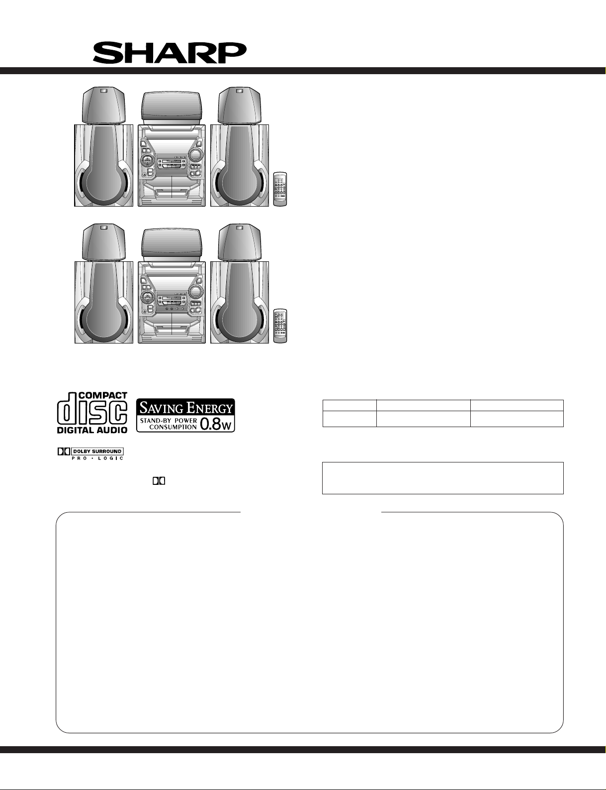
CD-DP2500W
CD-DP2500W/DK2500W
SERVICE MANUAL
No. S4034CDDP2500
CD-DP2500W
CD-DP2500W Mini Component System consisting of CDDP2500W (main unit), CP-DP2500 (front speakers),
GBOXS0038AWM1 (centre speaker) and GBOXS0039AWM1
(surround speakers).
CD-DK2500W
CD-DK2500W Mini Component System consisting of CDDK2500W (main unit), CP-DP2500 (front speakers),
GBOXS0038AWM1 (centre speaker) and GBOXS0039AWM1
(surround speakers).
CD-DK2500W
DIFFERENCE BETWEEN CD-DP2500W AND CD-DK2500W
SECTION CD-DP2500W CD-DK2500W
KARAOKE Non Used
Manufactured under license from Dolby Laboratories Licensing Corporation.
DOLBY, the double-D symbol and "PRO LOGIC" are
trademarks of Dolby Laboratories Licensing Corporation.
• In the interests of user-safety the set should be restored to its
original condition and only parts identical to those specified be
used.
CONTENTS
SAFETY PRECAUTION FOR SERVICE MANUAL ........................................................................................................... 2
VOLTAGE SELECTION..................................................................................................................................................... 2
SPECIFICATIONS ............................................................................................................................................................. 3
NAMES OF PARTS ........................................................................................................................................................... 4
OPERATION MANUAL ...................................................................................................................................................... 8
DISASSEMBLY.................................................................................................................................................................. 9
REMOVING AND REINSTALLING THE MAIN PARTS................................................................................................... 12
TEST MODE .................................................................................................................................................................... 13
ADJUSTMENT ................................................................................................................................................................. 14
NOTES ON SCHEMATIC DIAGRAM .............................................................................................................................. 16
BLOCK DIAGRAM ........................................................................................................................................................... 17
SCHEMATIC DIAGRAM / WIRING SIDE OF P.W.BOARD..............................................................................................20
VOLTAGE ........................................................................................................................................................................ 42
WAVEFORMS OF CD CIRCUIT...................................................................................................................................... 43
TROUBLESHOOTING (CD SECTION) ........................................................................................................................... 44
FUNCTION TABLE OF IC................................................................................................................................................ 48
FL DISPLAY......................................................................................................................................................................54
REPLACEMENT PARTS LIST/EXPLODED VIEW
Page
SHARP CORPORATION
This document has been published to be used
for after sales service only.
The contents are subject to change without notice.
Page 2
CD-DP2500W/DK2500W
SAFETY PRECAUTION FOR
SERVICE MANUAL
Precaution to be taken when replacing and servicing the
Laser Pickup.
The AEL (Accessible Emission Level) of Laser Power Output
for this model is specified to be lower than Class I Requirements.
However, the following precautions must be observed during
servicing to protect your eyes against exposure to the Laser
beam
(1) When the cabinet has been removed, the power is turned
on without a compact disc, and the Pickup is on a position
outer than the lead-in position, the Laser will light for several
seconds to detect a disc. Do not look into the Pickup Lens.
(2) The Laser Power Output of the Pickup inside the unit and
replacement service parts have already been adjusted prior
to shipping.
(3) No adjustment to the Laser Power should be attempted
when replacing or servicing the Pickup.
(4) Under no circumstances look directly into the Pickup Lens
at any time.
(5) CAUTION - Use of controls or adjustments, or performance
of procedures other than those specified herein may result
in hazardous radiation exposure.
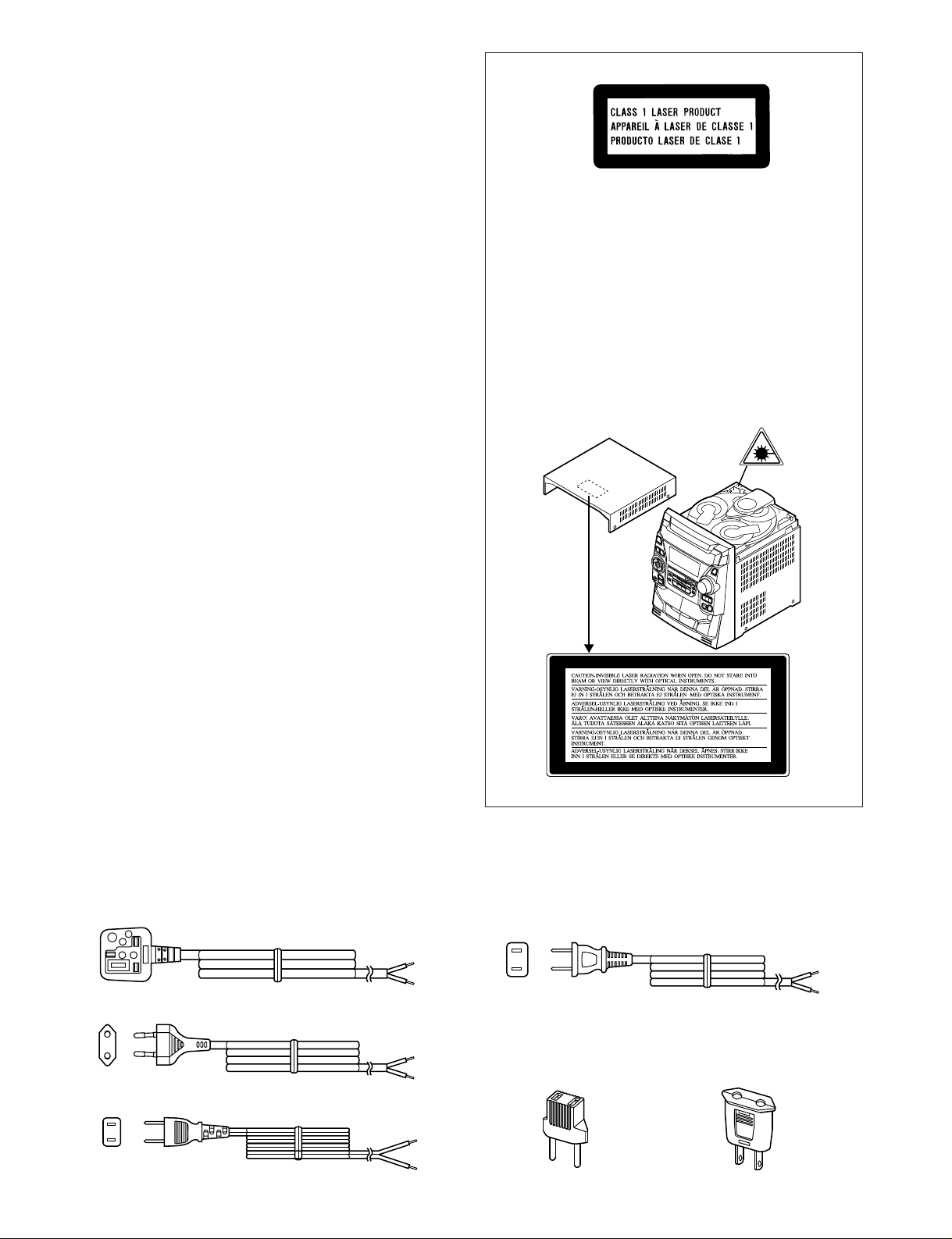
CAUTION
● This Mini Component System is classified as a CLASS 1
LASER product.
● The CLASS 1 LASER PRODUCT label is located on the
rear cover.
● Use of controls, adjustments or performance of proce-
dures other than those specified herein may result in hazardous radiation exposure.
As the laser beam used in this compact disc player is
harmful to the eyes, do not attempt to disassemble the
cabinet. Refer servicing to qualified personnel only.
Laser Diode Properties
Material: GaAIAs
Wavelength: 780 nm
Emission Duration: continuous
Laser Output: max. 0.6 mW
Illustration:CD-DP2500W
VOLTAGE SELECTION
The voltage selector is located on the AC voltage selector box. If adjustment is necessary, ensure to remove plug of AC cord from
AC socket and use a screwdriver in order to turn the selector in either direction. The correct voltage figure is displayed in the window
below to the adjustment screw.
QACCB0006AW00
QACCE0010AW00
QACCJ0007AW00
Figure 2 POWER SUPPLY CORD
– 2 –
QACCA0003AW00
QPLGA0003AWZZ QPLGA0004AWZZ
Page 3

FOR A COMPLETE DESCRIPTION OF THE OPERATION OF THIS UNIT, PLEASE REFER
TO THE OPERATION MANUAL.
SPECIFICATIONS
● General
Power source: AC 110/127/220/230-240 V, 50/60 Hz
Power consumption: 155 W
Dimensions: Width; 270 mm (10-5/8")
Height; 330 mm (13")
Depth; 332 mm (13-1/16")
Weight: 8.9 kg (19.6 lbs.)
● Amplifier section
Output power: Front speakers;
MPO; 200 W (100W + 100 W)
(10 % T.H.D.)
RMS; 120 W (60 W + 60 W)
(10 % T.H.D.)
RMS; 96 W (48 W + 48 W)
(0.9 % T .H.D.)
Centre speaker;
MPO; 50 W (10 % T.H.D.)
RMS; 30 W (10 % T.H.D.)
RMS; 24 W (0.9 % T.H.D.)
Surround speakers;
MPO; 50 W (25 W + 25 W)
(10 % T.H.D.)
RMS; 30 W (15 W + 15 W)
(10 % T.H.D.)
RMS; 24 W (12 W + 12 W)
(0.9 % T.H.D.)
Output terminals: Front speakers; 6 ohms
Centre speaker; 6 ohms
Surround speakers; 12 ohms
Headphones; 16-50 ohms
(recommended; 32 ohms)
CD digital output (optical)
Input terminals: Video/Auxiliary (audio signal) × 2;
(CD-DP2500W) 500 mV/47 kohms
Input terminals: Video/Auxiliary (audio signal) × 2;
(CD-DK2500W) 500 mV/47 kohms
Microphone 1/2; 1 mv/600 kohms
● Compact disc player section
Type: 3-disc multi-play compact disc player
Signal readout: Non-contact, 3-beam semiconductor
laser pickup
D/A converter: 1-bit D/A converter
Frequency response: 20 - 20,000 Hz
Dynamic range: 90 dB (1 kHz)
CD-DP2500W/DK2500W
● Tuner section
Frequency range: FM; 88-108 MHz
AM; 531-1,602 kHz
● Cassette deck section
Frequency response: 50-14,000 Hz (Normal tape)
Signal/noise ratio: 55 dB (TAPE 1, playback)
50 dB (TAPE 2, recording/playback)
Wow and flutter: 0.3 % (WRMS)
● Front speaker section
Type: 3-way type [13 cm (5-1/4") woofer,
5 cm (2") tweeter and super tweeter]
Maximum input
power: 120 W
Rated input power: 60 W
Impedance: 6 ohms
Dimensions: Width; 240 mm (9-1/2")
Height; 330 mm (13")
Depth; 255 mm (10-1/16")
Weight: 3.9 kg (8.5 lbs.)/each
● Centre speaker section
Type: 10 cm (4") full-range speaker
Maximum input
power: 60 W
Rated input power: 30 W
Impedance: 6 ohms
Dimensions: Width; 260 mm (10-1/4")
Height; 140 mm (5-1/2")
Depth; 155 mm (6-1/8")
Weight: 0.9 kg (2.0 lbs.)
● Surround speaker section
Type: 10 cm (4") full-range speaker
Maximum input
power: 30 W
Rated input power: 15 W
Impedance: 12 ohms
Dimensions: Width; 200 mm (7-7/8")
Height; 93 mm (3-11/16")
Depth; 170 mm (6-3/4")
Weight: 0.5 kg (1.1 lbs.)/each
Specifications for this model are subject to change without
prior notice.
– 3 –
Page 4
CD-DP2500W/DK2500W
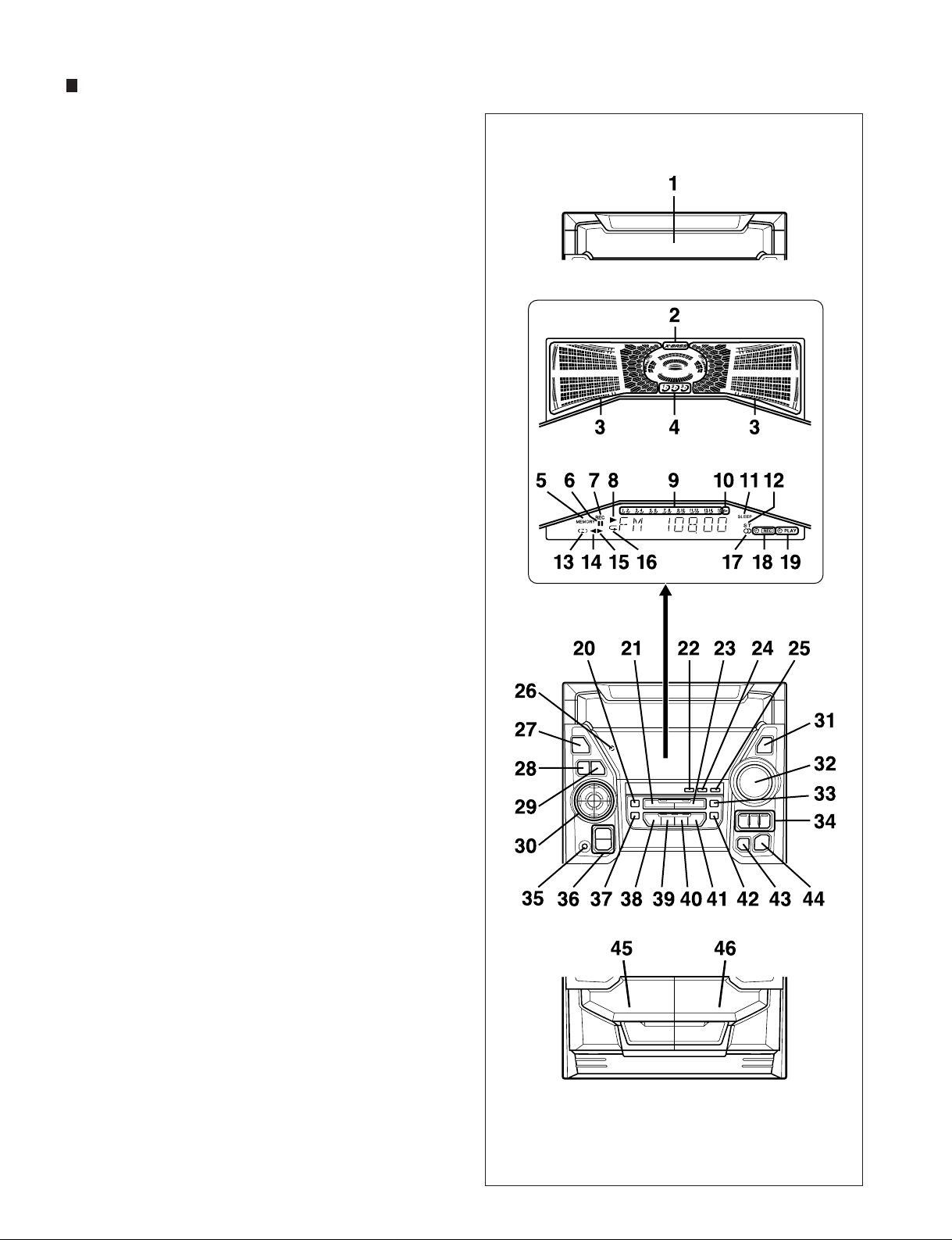
Front panel [CD-DP2500W]
1. (CD) Disc Tray
2. Extra Bass Indicator
3. Spectrum Analyzer/Volume Level Indicator
4. (CD) Disc Number Indicators
5. (CD/TUNER) Memory Indicator
6. (CD) Pause Indicator
7. (TAPE 2) Record Indicator
8. (CD) Play Indicator
9. (CD) Music Schedule Indicators
0. (CD) More Tracks Indicator
11. Sleep Indicator
12. FM Stereo Mode Indicator
13. (TAPE) Reverse Mode Indicator
14. (TAPE 2) Reverse Play Indicator
15. (TAPE 1) Play Indicator
(TAPE 2) Forward Play Indicator
16. (CD) Repeat Indicator
17. FM Stereo Indicator
18. Timer Record Indicator
19. Timer Play Indicator
NAMES OF PARTS
20. Memory/Set Button
21. (CD) Track Down/Review Button
(TUNER) Preset Down Button
(TAPE 2) Fast Wind Button
22. Bypass Button
23. (CD) Track Up/Cue Button
(TUNER) Preset Up Button
(TAPE 2) Fast Wind Button
24. Normal Button
25. Phantom Button
26. Timer Set Indicator
27. On/Stand-by Button
28. Clock Button
29. Timer/Sleep Button
30. Function Selector Buttons
31. Dimmer Button
32. Volume Control
33. Equalizer Mode Selector Button
34. (CD) Disc Number Select Buttons
35. Headphone Socket
36. Tuning and Time Up/Down Buttons
37. (TAPE 2) Record Pause Button
38. (TAPE 2) Reverse Play Button
39. (CD/TAPE) Stop Button
40. (TAPE 2) Reverse Mode Button
41. (CD) Play/Repeat Button
(TAPE 1) Play Button
(TAPE 2) Forward Play Button
42. Extra Bass/Demo Mode Button
43. (CD) Disc Skip Button
44. (CD) Open/Close Button
45. (TAPE 1) Cassette Compartment
46. (TAPE 2) Cassette Compartment
– 4 –
Page 5
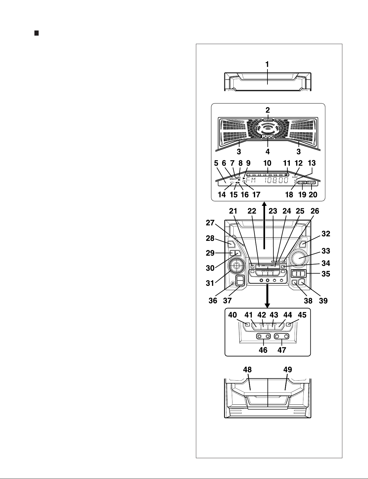
Front panel [CD-DK2500W]
1. (CD) Disc Tray
2. Extra Bass Indicator
3. Spectrum Analyzer/Volume Level Indicator
4. (CD) Disc Number Indicators
5. Karaoke Maker Indicator
6. (CD/TUNER) Memory Indicator
7. (CD) Pause Indicator
8. (TAPE 2) Record Indicator
9. (CD) Play Indicator
(CD) Music Schedule Indicators
(CD) More Tracks Indicator
12. Sleep Indicator
13. FM Stereo Mode Indicator
14. (TAPE) Reverse Mode Indicator
15. (TAPE 2) Reverse Play Indicator
16. (TAPE 1) Play Indicator
(TAPE 2) Forward Play Indicator
17. (CD) Repeat Indicator
18. FM Stereo Indicator
19. Timer Record Indicator
20. Timer Play Indicator
CD-DP2500W/DK2500W
21. Memory/Set Button
22. (CD) Track Down/Review Button
(TUNER) Preset Down Button
(TAPE 2) Fast Wind Button
23. Bypass Button
24. (CD) Track Up/Cue Button
(TUNER) Preset Up Button
(TAPE 2) Fast Wind Button
25. Normal Button
26. Phantom Button
27. Timer Set Indicator
28. On/Stand-by Button
29. Clock Button
30. Timer/Sleep Button
31. Function Selector Buttons
32. Dimmer Button
33. Volume Control
34. Equalizer Mode Selector Button
35. (CD) Disc Number Select Buttons
36. Headphone Socket
37. Tuning and Time Up/Down Buttons
38. (CD) Disc Skip Button
39. (CD) Open/Close Button
40. (TAPE 2) Record Pause Button
41. (TAPE 2) Reverse Play Button
42. (CD/TAPE) Stop Button
43. (TAPE 2) Reverse Mode Button
44. (CD) Play/Repeat Button
(TAPE 1) Play Button
(TAPE 2) Forward Play Button
45. Extra Bass/Demo Mode Button
46. Microphone Sockets
47. Microphone Level Controls
48. (TAPE 1) Cassette Compartment
49. (TAPE 2) Cassette Compartment
– 5 –
Page 6
CD-DP2500W/DK2500W
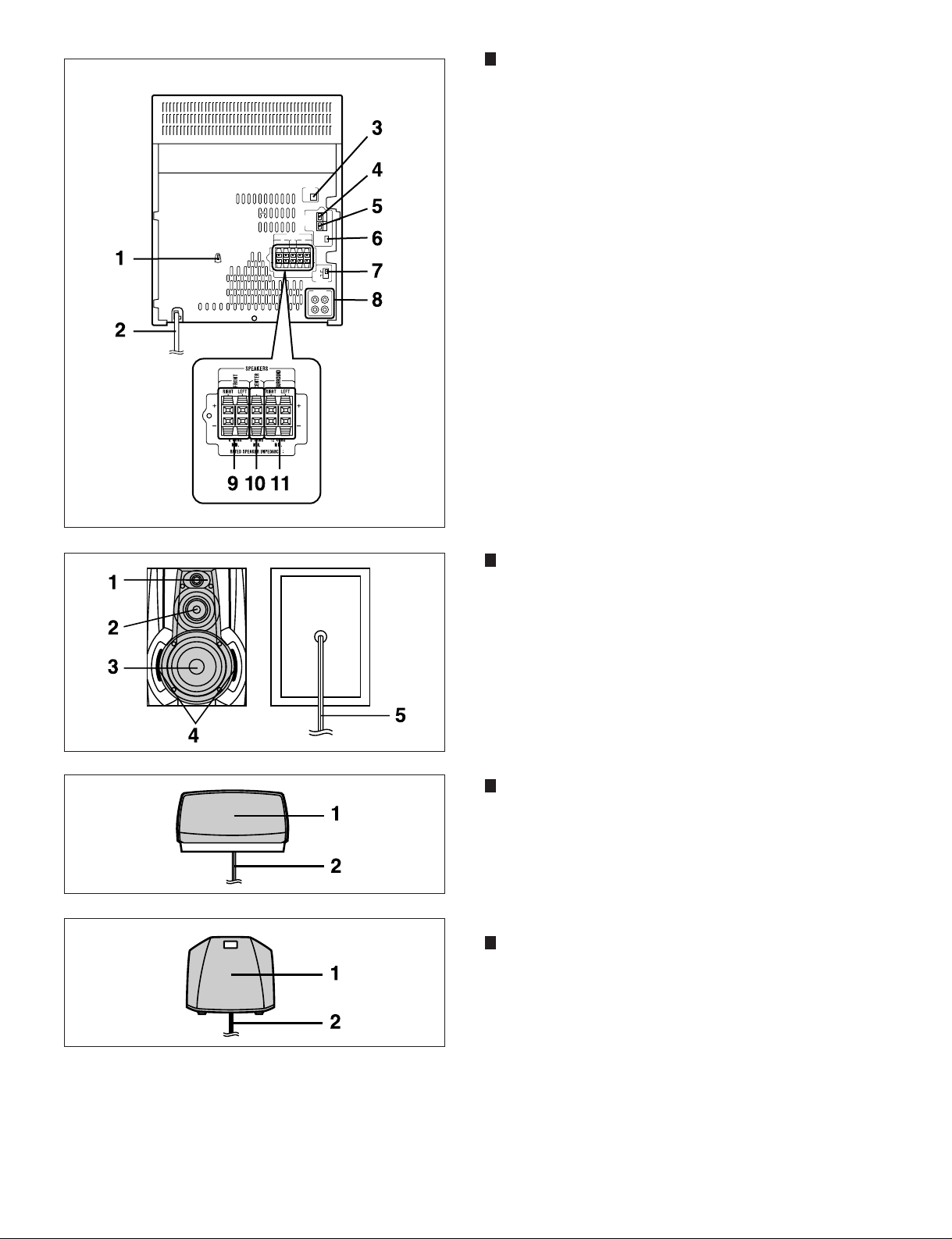
Rear panel
1. AC Voltage Selector
2. AC Power Lead
3. CD Digital Output Socket
4. FM 75 Ohms Aerial Terminal
5. FM Aerial Earth Terminal
6. AM Loop Aerial Input Socket
7. Span Selector Switch
8. Video/Auxiliary (Audio Signal) Input Sockets
9. Front Speaker Terminals
10. Centre Speaker Terminals
11. Surround Speaker Terminals
Front speaker
1. Super Tweeter
2. Tweeter
3. Woofer
4. Bass Reflex Ducts
5. Speaker Wire
Centre speaker
1. Full-Range Speaker
2. Speaker Wire
Surround speaker
1. Full-Range Speaker
2. Speaker Wire
– 6 –
Page 7
CD-DP2500W/DK2500W
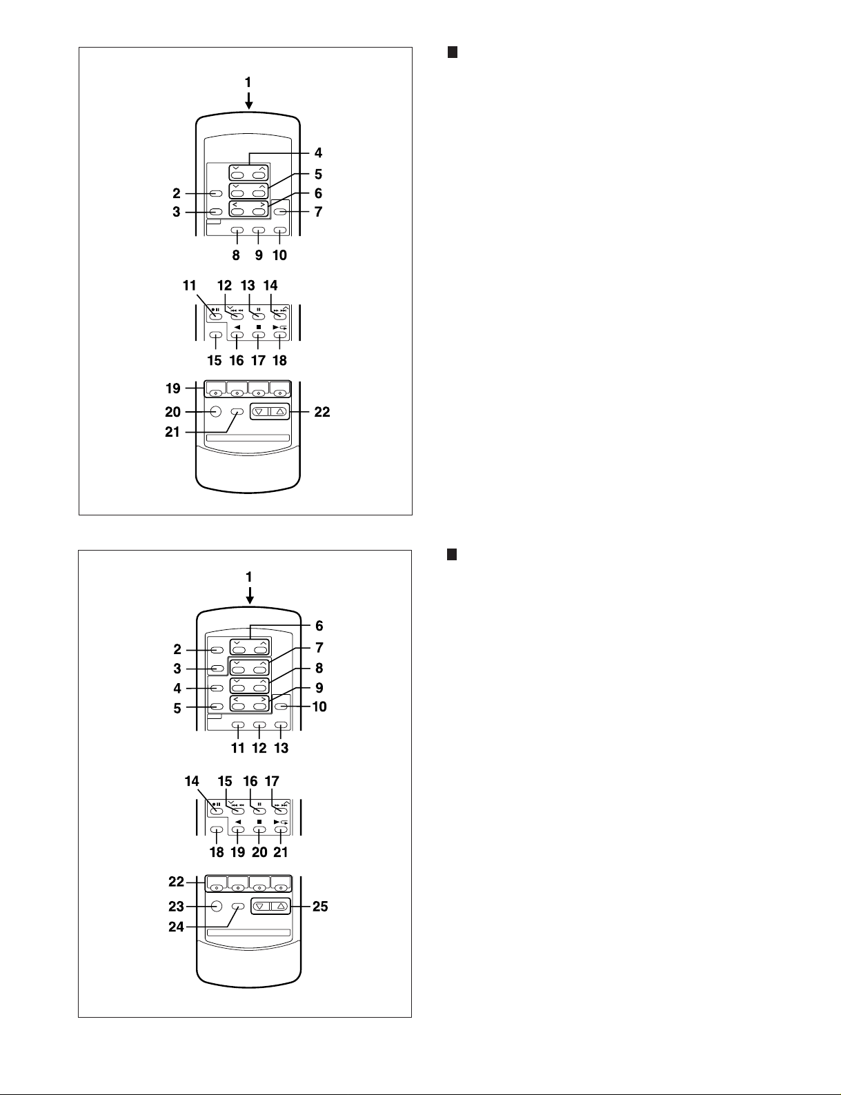
Remote control [CD-DP2500W]
1. Remote Control Transmitter LED
2. Dolby Pro Logic Surround Mode Button
3. Test Tone Button
4. Centre Level Buttons
5. Surround Level Buttons
6. Balance Control Buttons
7. (CD) Disc Skip Button
8. (CD) Clear Button
9. (CD) Memory Button
10. (CD) Random Button
11. (TAPE 2) Record Pause Button
12. (CD) Track Down/Review Button
(TUNER) Preset Down Button
(TAPE 2) Fast Wind Button
13. (CD) Pause Button
14. (CD) Track Up/Cue Button
(TUNER) Preset Up Button
(TAPE 2) Fast Wind Button
15. Equalizer Mode Selector Button
16. (TAPE 2) Reverse Play Button
17. (CD/TAPE) Stop Button
18. (CD) Play/Repeat Button
(TAPE 1) Play Button
(TAPE 2) Forward Play Button
19. Function Selector Buttons
20. On/Stand-by Button
21. Extra Bass Button
22. Volume Up/Down Buttons
Remote control [CD-DK2500W]
1. Remote Control Transmitter LED
2. Karaoke Mode Button
3. Vocal Replacer Button
4. Dolby Pro Logic Surround Mode Button
5. Test Tone Button
6. Echo Level Up/Down Buttons
7. Centre Level Buttons
8. Surround Level Buttons
9. Balance Control Buttons
10. (CD) Disc Skip Button
11. (CD) Clear Button
12. (CD) Memory Button
13. (CD) Random Button
14. (TAPE 2) Record Pause Button
15. (CD) Track Down/Review Button
(TUNER) Preset Down Button
(TAPE 2) Fast Wind Button
16. (CD) Pause Button
17. (CD) Track Up/Cue Button
(TUNER) Preset Up Button
(TAPE 2) Fast Wind Button
18. Equalizer Mode Selector Button
19. (TAPE 2) Reverse Play Button
20. (CD/TAPE) Stop Button
21. (CD) Play/Repeat Button
(TAPE 1) Play Button
(TAPE 2) Forward Play Button
22. Function Selector Buttons
23. On/Stand-by Button
24. Extra Bass Button
25. Volume Up/Down Buttons
– 7 –
Page 8
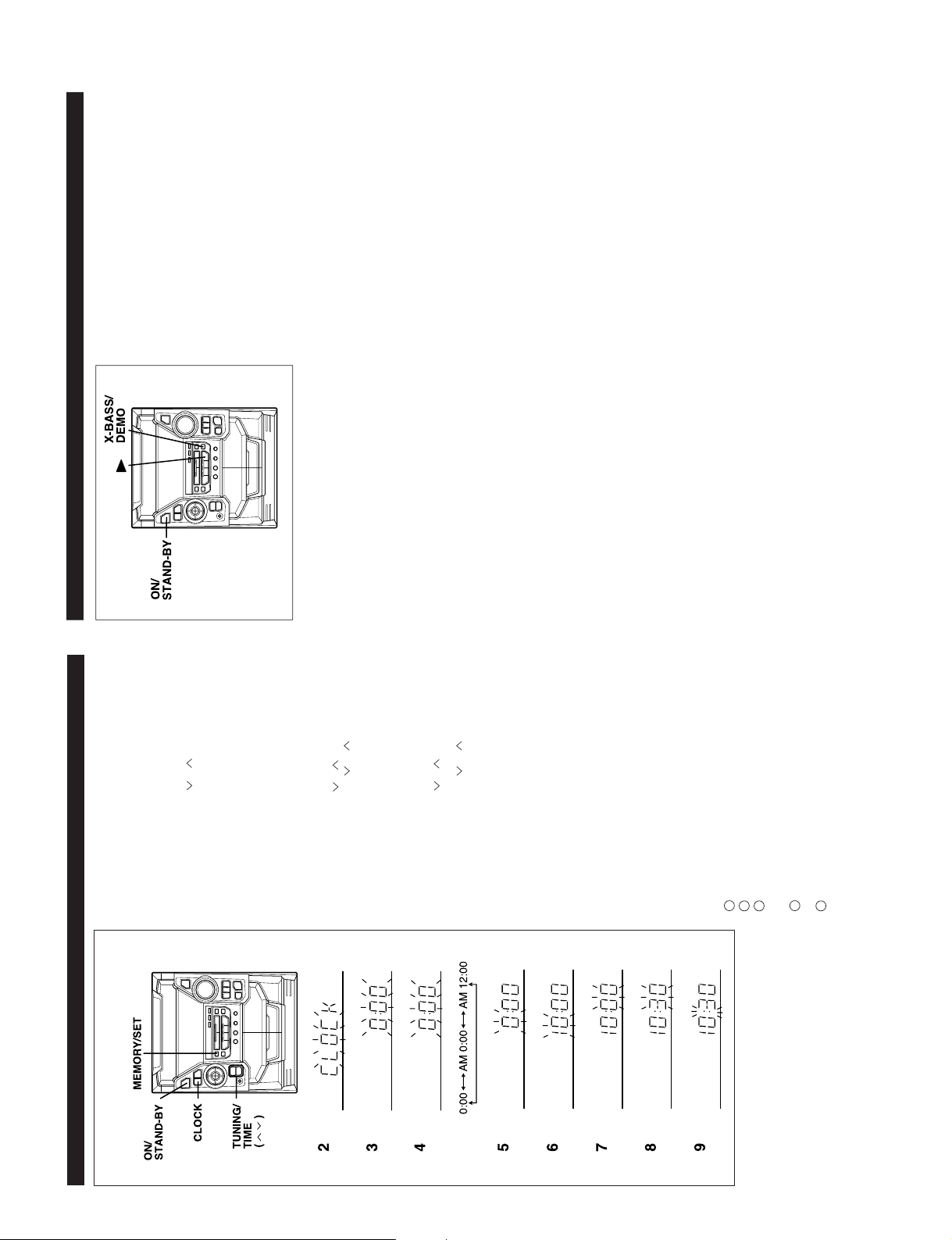
CD-DP2500W/DK2500W
SETTING THE CLOCK
In this example, the clock is set for the 24-hour (0:00) system.
1
Press the ON/STAND-BY button to enter the stand-by mode.
2
Press the CLOCK button.
3
Within 5 seconds, press the MEMORY/SET button.4Press the TUNING/TIME (
or ) button to select the time
display mode.
“0:00” →The 24-hour display will appear.
(0:00 - 23:59)
“AM 0:00” →The 12-hour display will appear.
(AM 0:00 - PM 11:59)
“AM 12:00” →The 12-hour display will appear.
(AM 12:00 - PM 11:59)
● Note that this can only be set when the unit is first in-
stalled or it has been reset.
5
Press the MEMORY/SET button.6Press the TUNING/TIME (
or ) button to adjust the hour.
● Press the TUNING/TIME ( or ) button once to ad-
vance the time by 1 hour. Hold it down to advance con-
tinuously.
● When the 12-hour display is selected, “AM” will change
automatically to “PM”.
7
Press the MEMORY/SET button.8Press the TUNING/TIME (
or ) button to adjust the min-
utes.
● Press the TUNING/TIME (
or
) button once to ad-
vance the time by 1 minute. Hold it down to change the
time in 5 minute intervals.
● The hour setting will not advance even if minutes advance
from “59” to “00”.
9
Press the MEMORY/SET button.
● The clock starts operating from “0” second.
(Seconds are not displayed.)
And then the clock display will disappear after a few sec-
onds.
To see the time display:
Press the CLOCK button.
● The time display will appear for about 5 seconds.
Note:
● The clock display will flash on and off at the push of the
CLOCK button when the AC power supply is restored after
a power failure occurs or after the AC power lead is discon-
nected.
If this happens, follow the procedure below to change the
clock time.
To change the clock time:
1 Press the CLOCK button.
2 Within 5 seconds, press the MEMORY/SET button.
3
Perform steps 6 - 9 above.
To change the time display mode:
1 Perform steps 1 - 2 in the section “RESETTING THE MI-
CROCOMPUTER”.
2
Perform steps 1 - 9 above.
(Main unit operation)
RESETTING THE MICROCOMPUTER
Reset the microcomputer under the following con-
ditions:
● To erase all of the stored memory contents (clock and timer
settings, and tuner and CD presets).
● If the display is not correct.
● If the operation is not correct.
1
Press the ON/STAND-BY button to enter the stand-by mode.
2
Whilst pressing down the 0 button and the X-BASS/ DEMO
button, hold down the ON/STAND-BY button for at least 1
second.
● “CLEAR AL” will appear.
Caution:
● The operation explained above will erase all data stored in
memory including clock and timer settings, and tuner and
CD presets.
OPERATION MANUAL
Illustration:CD-DP2500W
Illustration:CD-DP2500W
– 8 –
Page 9
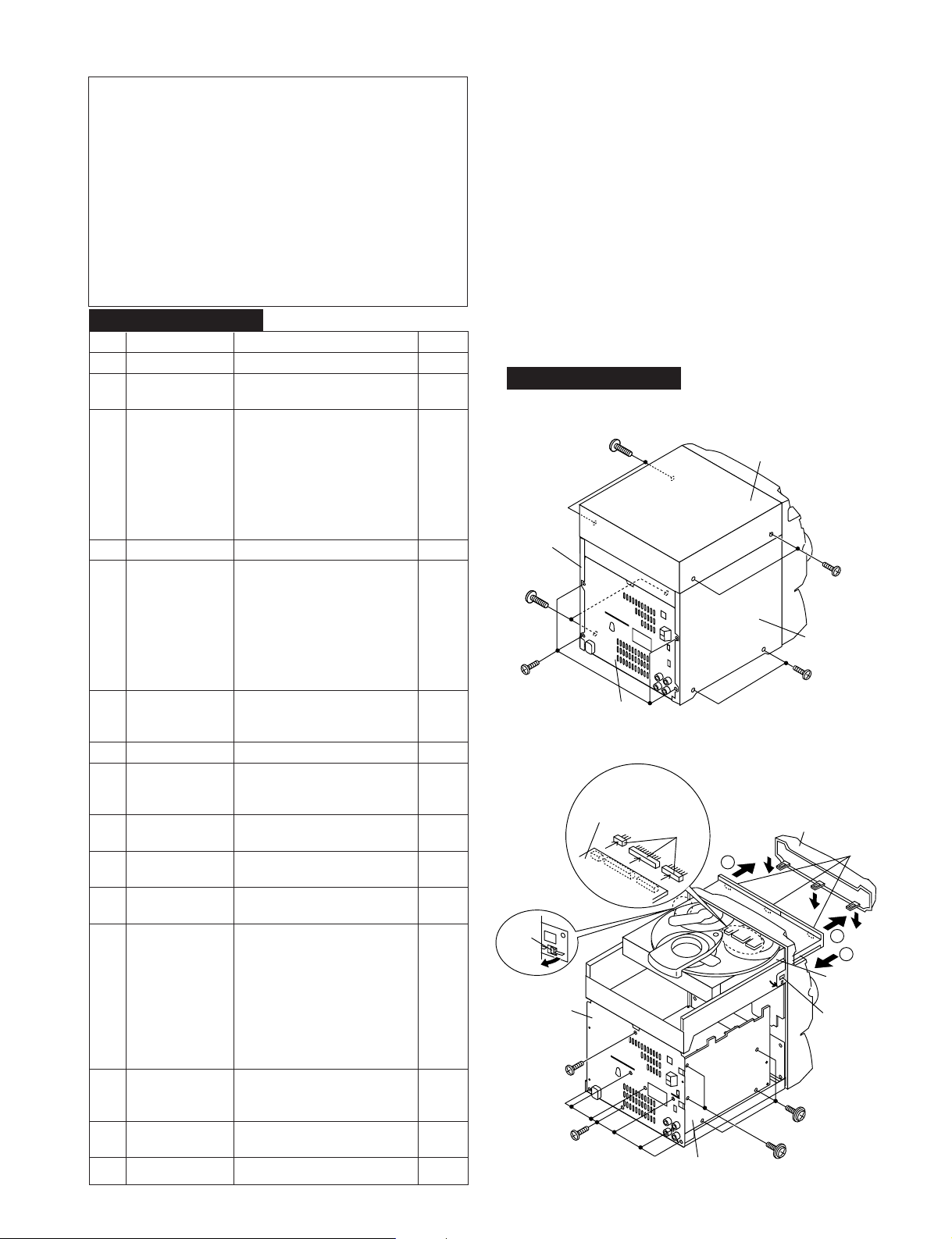
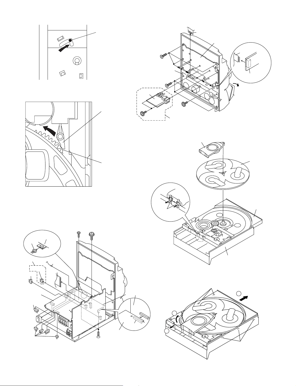
DISASSEMBLY
Caution on Disassembly
Follow the below-mentioned notes when disassembling
the unit and reassembling it, to keep it safe and ensure
excellent performance:
1. Take cassette tape and compact disc out of the unit.
2. Be sure to remove the power supply plug from the wall
outlet before starting to disassemble the unit.
3. Take off nylon bands or wire holders where they need be
removed when disassembling the unit. After servicing
the unit, be sure to rearrange the leads where they were
before disassembling.
4. Take suffcient care on static electricity of integrated
circuits and other circuits when servicing.
CD-DP2500H/DK2500W
STEP
10
11 Turntable 1. Hook....................... (L1) x2 10-5
12 Disc Tray 1.
13 CD Servo PWB 1. Screw ..................... (N1) x1 11-1
14 CD Mechanism 1. Hook ....................... (P1) x2 11-2
15
REMOVAL PROCEDURE FIGURE
1 Top Cabinet 1. Screw ..................... (A1) x4 9-1
2 Side Panel 1. Screw ..................... (B1) x8 9-1
(Left/right)
3 CD Player Unit/ 1. Turn on the power supply, 9-2
CD Tray Cover open the disc tray, take out
the CD cover, and close.
(Note 1)
2. Screw ..................... (C1) x1
3. Hook....................... (C2) x3
4. Hook....................... (C3) x2
5. Socket .................... (C4) x3
4 Rear Panel 1. Screw ..................... (D1) x9 9-2
5 Main PWB 1. Screw ..................... (E1) x3 9-2
6
Power Supply PWB
7 Front Panel 1. Screw ..................... (G1) x2 10-3
8 Karaoke PWB 1. Screw..................... (H1) x2 10-4
(CD-DK25000W
ONLY)
9 Display PWB/ 1. Screw .....................
Headphones PWB
Tape Mechanism
(Note 2) 2. Hook....................... (N2) x2
Loading Motor PWB
2. Socket .................... (E2) x2 10-3
(CD-DP25000W)
2. Socket .................... (E2) x3
(CD-DK25000W)
3. Flat Cable .............. (E3) x1
4. Lug Wire................. (E4) x1
5. Socket .................... (E5) x1
1. Screw ..................... (F1) x2 10-3
2. Socket .................... (F2) x5
3. Flat Wire................. (F3) x1 10-4
(J1) x15
2. Flat Cable .............. (J2) x1
1. Open the cassette holder 10-4
2. Screw ..................... (K1) x5
2. Cover ..................... (L2) x1
Turn fully the lock lever in the
arrow direction.
2.
While holding the lock lever,rotate
the cam gear until the cam gear
rib engages with the clamp lever.
3.
Push the slide holder backward to
engage the claw with the groove
and remove it in the direction
of the arrow. ..............
3. Socket .................... (N3) x4
2. Hook....................... (P2) x3
1. Hook....................... (Q1) x5 11-2
(M1) x6
10-4
10-1
10-2
10-6
CD-DP2500W/DK2500W
Note 1:
How to open the changer manually. (Fig. 10-1)
1. In this state, turn fully the lock lever in the arrow direction
through the hole on the loading chassis bottom.
2.
While holding the lock lever, rotate the cam gear anticlockwise
until the cam gear rib engages with the clamp lever.
3. After that, push forward the CD slide holder.
Note 2:
1. After removing the connector for the optical pickup from the
connector, wrap the conductive aluminium foil around the
front end of the connector so as to protect the optical pickup
from electrostatic damage.
Note 3:
1. Be careful not to break the claw of the CD mechanism.
2. When fining back the cam gear assembly, let it lock by front
movement.
CD-DP2500H/DK2500W
– 9 –
Side Panel
(Right)
(B1)x2
ø3x10mm
(B1)x4
ø3x10mm
(C3) x1
Pull
(C1)x1
ø3x10mm
(D1)x7
ø3x10mm
Rear
Panel
(A1)x2
ø3x12mm
CD Servo
PWB
Rear
Panel
Figure 9-1
(C4)x3
Main PWB
Figure 9-2
Top Cabinet
(B1)x2
ø3x10mm
DC Tray Cover
1
(D1)x2
ø3x10mm
(Fig. 10-2)
(A1)x2
ø3x12mm
Side Panel
(Left)
(C2) x3
1
2
CD Player
Unit
(C3)x1
(E1)x3
ø3x10mm
Page 10
CD-DP2500W/DK2500W
Figure 10-1
LOCK LEVER
CLAMP LEVER
CAM GEAR RIB
Karaoke
PWB
(H1)x1
ø3x10mm
(J1)x14
ø3x10mm
Tape
Mechanism
(K1)x5
ø3x10mm
(J1)x1
ø3x10mm
CD-DK2500W
ONLY
(J2)x1
Display PWB
(F3)x1
Headphones
PWB
Open
Cassette
Holder
Figure 10-4
(L2) x1
Turntable
(E5)x1
CD-DK2500W
ONLY
(E2)x1
(E2)x1
Power
Supply
PWB
(F2)x1
(F2)x4
Tape
Mechanism
(E4)x1
(E3)x1
Figure 10-2
(F1)x1
ø3x6mm
(F1)x1
ø3x10mm
(G1)x2
ø3x10mm
Power
Supply
PWB
Main PWB
(E2)x1
(L1) x2
Disc Tray
CD Player Unit
Figure 10-5
(M1) x3
3
2
1
(M1) x3
Figure 10-3
Figure 10-6
– 10 –
Page 11
CD-DP2500W/DK2500W
Screw Driver
Woofer
(A1)x1
(B1)x4
Ø4x12mm
(C1)x2
Ø3x10mm
(D1)x2
Ø3x10mm
(N1)x1
ø3x8mm
(N2) x2
(N3) x2
(N3) x2
CD Servo
PWB
Figure 11-1
CD Player
Base
CD
Mechanism
(P1) x1
(P2) x3
(P1) x1
Figure 11-2
Loading
Motor
PWB
(Q1) x5
CP-DP2500
STEP
REMOVAL PROCEDURE FIGURE
1 Front Panel 1. Front Panel ............ (A1) x1 11-3
2 Woofer 1. Screw ..................... (B1) x4 11-3
4 Tweeter 1. Screw .................... (C1) x2 11-3
5 Super Tweeter 1. Screw .................... (D1) x2 11-3
CP-DP2500
Figure 11-3
– 11 –
Page 12
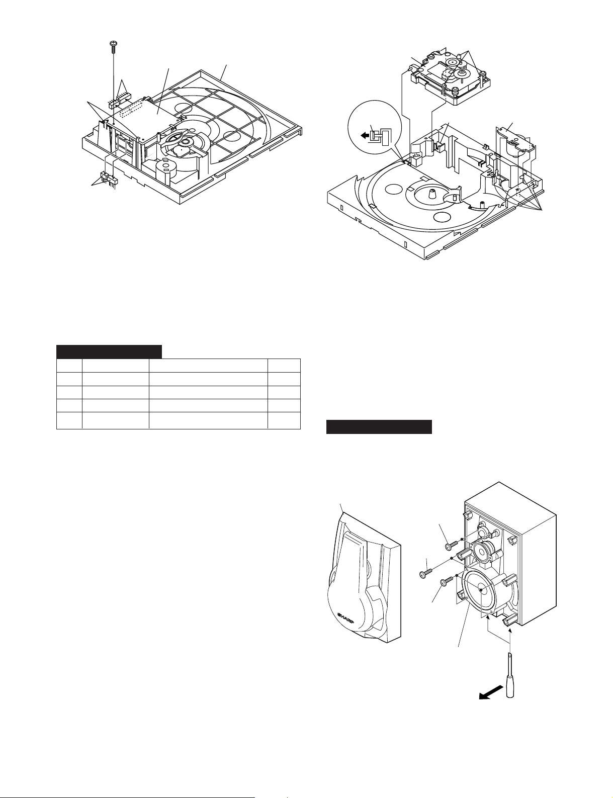
CD-DP2500W/DK2500W
REMOVING AND REINSTALLING THE MAIN PARTS
TAPE MECHANISM SECTION
Perform steps 1 to 7 and 10 of the disassembly method to
remove the tape mechanism.
How to remove the record/playback and erase
heads (TAPE 2) (See Fig. 12-1)
1. When you remove the screw (A1) x 2 pcs., the recording/
playback head and three-dimensional head of the erasing
head can be removesd.
How to remove the playback head (TAPE 1)
(See Fig. 12-2)
1. When you remove the screw (B1) x 2 pcs., the playback
head.
Erase Head
(A1)x2
Ø2 x 5mm
TAPE 2
Figure 12-1
TAPE 1
Record/Playback
Head
How to remove the pinch roller (TAPE 1/2)
(See Fig. 12-3)
1. Carefully push the inside claw to remove it. The pinch roller
pawl in the direction of the arrow <A>, and remove the pinch
roller (C1) x 1 pc., in the direction of the arrow <B>.
Note:
When installing the pinch roller, pay attention to the spring
mounting position.
How to remove the belt (TAPE 1) (See Fig. 12-4)
1. Remove the main belt (D1) x 1 pc., from the motor side.
2. Remove the FF/REW belt (D2) x 1 pc.
How to remove the belt (TAPE 2) (See Fig. 12-4)
1. Remove the main belt (E1) x 1 pc., from the motor side.
2. Remove the FF/REW belt (E2) x 1 pc.
How to remove the motor (See Fig. 12-5)
1. Remove the screws (F1) x 2 pcs., to remove the motor.
(B1)x2
Ø2 x 9mm
Pinch Roller
(C1)x1
Figure 12-2
<B>
Figure 12-3
Playback
Head
Pinch Roller
Pawl
<A>
(F1) x2
Ø 2.6 x 5mm
Motor
– 12 –
TAPE2
FF/REW
Belt
(E2)x1
Main Belt
Figure 12-4Figure 12-5
Motor
TAPE2
Main Belt
(E1)x1
Motor
TAPE1
Main Belt
(D1)x1
TAPE1
FF/REW
Belt
(D2)x1
Page 13
CD MECHANISM SECTION
Perform steps 1, 2, 3, and 11 to 14 of the disassembly method
to remove the CD mechanism.
CD-DP2500W/DK2500W
How to remove the loading motor
(See Fig. 13-1)
1. Bend the hooks (A1) x 5 pcs., to remove the loading motor.
How to remove the pickup (See Fig. 13-2)
1. Remove the stop washer (B1) x 1 pc., to remove the gear
(B2).
2. Remove the screws (B3) x 2 pcs., to remove the shaft (B4).
3. Remove the pickup.
Note
After removing the connector for the optical pickup from the
connector wrap the conductive aluminium foil around the front
end of connector so as to protect the optical pickup from
electrostatic damage.
(B1) x2
ø2.6 x6mm
Loading Motor
(A1)x1
(A1)x2
(A1)x2
CD Base
Figure 13-1
Stop Washer
(B3) x1
TEST MODE
During POWER OFF mode,push below each 2 keys [ON/STAND-BY] key.
Then go to each TEST MODE.
KEY TEST MODE CONTENTS
[ON/STAND-BY] [TUNER] + [X-BASS] TEST 1 TUNER PRESET MEMORY CLEAR
[ON/STAND-BY] [MEMORY/SET] + [X-BASS] TEST 2 TUNER PRESET FOR PRODUCTION
[ON/STAND-BY] [>>] + [X-BASS] TEST 3 KEY AND DISPLAY TEST
[ON/STAND-BY] [CD] + [X-BASS] TEST 4 CD TEST MODE
[ON/STAND-BY] [TAPE] + [X-BASS] TEST 5 TAPE TEST MODE
[ON/STAND-BY] [>] + [X-BASS] TEST 6 ALL CLEAR(RESET)
Shaft
(B2) x1
Pickup
CD Mechanism
Gear
(B4) x1
Figure 13-2
[ON/STAND-BY] [TUN UP] + [X-BASS] TEST 7 AUDIO TEST
[ON/STAND-BY] [TUN DOWN] + [X-BASS] TEST 8 PRODUCTION INITIALIZE FOR CHANGER
– 13 –
Page 14
CD-DP2500W/DK2500W
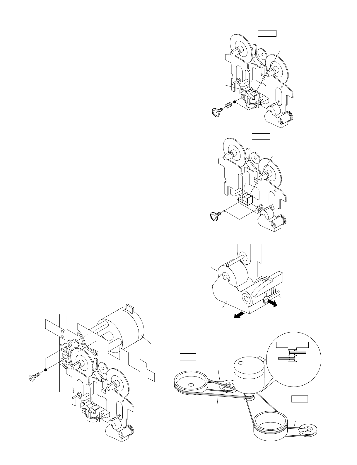
ADJUSTMENT
MECHANISM SECTION
• Driving Force Check
Torque Meter
Play: TW-2111 Tape 1: Over 80 g
• Torque Check
Torque Meter
Tape 1
Play: TW-2111 30 to 80 g. cm 30 to 80 g.cm
Fast forward: TW-2231 — 70 to 180 g.cm
Rewind: TW-2231 — 70 to 180 g.cm
TUNER SECTION
fL: Low-range frequency
fH: High-renge frequency
• AM IF/RF
Signal generator: 400 Hz, 30%, AM modulated
Test Stage
Frequency
AM IF 450 kHz 1,602 kHz T351 *1
AM Band — 531 kHz (fL): T306 *2
Coverage 1.1 ± 0.1 V
AM Tracking 990 kHz 990 kHz (fL): T303 *1
Frequency
Display
*1. Input: Antenna,SO301 Output: TP302
*2. Input: Antenna,SO301 Output: TP301
CD SECTION
• Adjustment
Since this CD system incorporates the following automatic
adjustment functions, readjustment is not needed when
replacing the pickup. Therefore, different PWBs and pickups
can be combined freely.
Each time a disc is changed, these adjustments are
performed automatically. Therefore, playback of each disc
can be performed under optimum conditions.
Items adjusted automatically
(1) Offset adjustment (The offset voltage between the head
amplifier output and the VREF reference voltage is
compensated inside the IC.)
* Focus offset adjustment
* Tracking offset adjustment
(2) Tracking balance adjustment (waveform drawing 14-3
EFBL)
(3) Gain adjustment (The gain is compensated inside the IC
so that the loop gain at the gain crossover frequency will
be 0dB.)
* Focus gain adjustment
* Tracking gain adjustment
Specified Value
Tape 2: Over 80 g
Specified Value
Setting/
Adjusting
Parts
Tape 2
Instrument
Connection
• Tape Speed
Test Tape
Adjusting
Point
Normal MTT-111 Variable 3,000 ± Speaker
speed Resistor in 30 Hz terminal
motor. (Load
(MM1) resistance:
TAPE MECHANISM
Variable Resistor in motor
Specified
Value
Motor
Figure 14-1
MAIN PWB
IC302
CF351
R357
AM IF
T351
IC303
TP302
CF352
C393
T301
CF302
T306
AM Band Coverage
TP301
T302
L312
C375
IC301
T303
AM Tracking
CNP301
Figure 14-2 ADJUSTMENT POINT
CD ERROR CODE DESCRIPTION
Error State Code
0001 Cannot detect Pickup-in SW
0002 DSP access error
0101 Open/Close SW not functioning (Low → High)
0103 Open/Close SW not functioning (High → Low)
0201 Open/Close SW not functioning (Low → High)
0203 Open/Close SW not functioning (High → Low)
0302 Pickup-in SW is not detected
0306 During Disc 1 search, Open/Close SW or Clamp SW
0307 Clamp SW not function (Low → High)
0308 Clamp SW not function (High → Low)
– 14 –
[Servo System Error]
[Error during close operation]
[Error during open operation]
[Error during skip operation]
or Disc SW do not change to low.
T
Stopped
CH1=500mV
CH2=200mV
DC 10:1
DC 10:1
T
FDO
1
TE
3
EFBL
2
Smoothing : ON CH1 : 0.000V
BW : FULL
CH2 : 0.000V
CH3 : 0.00V
CH4 : 0.00V
CH3=1V
DC 10:1
=Record Length=
Main : 100K
Zoom : 2k
1999/04/05 20:26:47
500ms/div
(500ms/div)
NORM:20kS/s
=Trigger==Filter= =Offset=
Mode : SINGLE
Type : EDGE CH1
Delay : 0.0ns
Hold off : 0.2us
Figure 14-3
CH2
v/DIV
200mV
SO301
FM75 ohms
GND
AM LOOP
ANTENNA
Instrument
Connection
6 ohms)
Page 15
CD-DP2500W/DK2500W
EXPLANATION OF DOLBY SURROUND PRO LOGIC AND EVALUATION METHOD
Outline
• Namely, two speakers are connected in parallel to one
amplifier.
• In the Pro Logic BYPASS mode the amplifier for C-ch (center
channel) and the amplifier for S-ch (surround channel) are in
MUTE state. The SP output is cut.
• State of element output and terminal output in specific mode
State of set Dolby Pro Logic Dolby Pro Logic On mode
Output point Bypass mode Normal mode Phantom mode
IC501 1 pin L-out Output enabled state Output enabled state Output enabled state
2 pin R-out Output enabled state Output enabled state Output enabled state
IC501 3pin C-out No output Output enabled state No output
IC501 9pin S-out No output Output enabled state Output enabled state
SP OUT L-ch Output enabled state Output enabled state Output enabled state
(SO901) R-ch Output enabled state Output enabled state Output enabled state
SP OUT C-ch No output in MUTE (Q501) state Output enabled state No output in MUTE (Q501) state
(SO901)
SP OUT S-ch No output in MUTE (Q502) state Output enabled state Output enabled state
(SO901)
Test tone output
• Pro Logic ON Normal mode
Press the remote control TEST TONE button.
→Output of only L-ch →Output of only C-ch
↑ ↓
Output of only S-ch ← Output of only R-ch
The test tone (noise) is repeatedly output for output period
(2 sec).
In this case the following indication appears repeatedly.
→TEST →L-ch →C-ch
↑ ↓
S-ch ← R-ch
• Pro Logic ON Phantom mode
Press the remote control TEST TONE button.
→Output of only L-ch →Output of only R-ch
↑ ↓
← Output of only S-ch
The test tone (noise) is repeatedly output for output period
(2 sec).
In this case the following indication appears repeatedly.
→TEST → L-ch → R-ch
↑ ↓
← S-ch←
Relation between VIDEO IN input and output in Pro Logic
ON state
(1) L-ch/R-ch same phase input into VIDEO IN input jack in
VIDEO Function mode
Output point Normal mode
SP out L-ch Almost no output (only omitting component)
(SO901) R-ch Almost no output (only omitting component)
(SO901) SP out C-ch
(SO901) SP out S-ch
Input signal is output.
Almost no output (only omitting component)
• In the normal mode of Pro Logic ON mode the amplifiers for
C-ch and S-ch are in operative state, so that the SP output
appears.
• In the Phantom mode of Pro Logic ON mode the amplifier for
C-ch is in MUTE state, so that the SP output is cut. The
amplifier for S-ch (surround) is in operative state, so that the
SP output appears
Output point Phantom mode
SP out L-ch Input signal is output.
(SO901) R-ch Input signal is output.
(SO901) SP out C-ch SP cut, no output
(SO901) SP out S-ch
Almost no output (only omitting component)
(2) L-ch/R-ch reverse phase input into VIDEO IN input jack in
VIDEO Function mode
(Reverse phase: Phase difference between L and R is 180°)
Output point Normal mode
SP out L-ch
(SO901) R-ch
(SO901) SP out C-ch
(SO901) SP out S-ch Input signal is output.
Output point Phantom mode
SP out L-ch
(SO901) R-ch
(SO901) SP out C-ch SP cut, no output
(SO901) SP out S-ch Input signal is output.
Almost no output (only omitting component)
Almost no output (only omitting component)
Almost no output (only omitting component)
Almost no output (only omitting component)
Almost no output (only omitting component)
• Accordingly, if you want to output signal waveform to C-ch SP
out, give the same phase input into L-ch/R-ch INPUT in the
Pro Logic Normal mode.
If one of channels receives input, C-ch does not output. Only
L-ch or R-ch outputs.
• If you want to output signal waveform to S-ch SP out, you can
use either Normal mode or Phantom mode. However, 180°
reverse phase input must be given to L-ch/R-ch INPUT.
– 15 –
Page 16
CD-DP2500W/DK2500W
NOTES ON SCHEMATIC DIAGRAM
• Resistor:
To differentiate the units of resistors, such symbol as K and
M are used: the symbol K means 1000 ohm and the symbol
M means 1000 kohm and the resistor without any symbol is
ohm-type resistor. Besides, the one with “Fusible” is a fuse
type.
• Capacitor:
To indicate the unit of capacitor, a symbol P is used: this
symbol P means micro-micro-farad and the unit of the
capacitor without such a symbol is microfarad. As to
electrolytic capacitor, the expression “capacitance/withstand
voltage” is used.
(CH), (TH), (RH), (UJ): Temperature compensation
(ML): Mylar type
(P.P.): Polypropylene type
• Schematic diagram and Wiring Side of P.W.Board for this
model are subject to change for improvement without prior
notice.
• The indicated voltage in each section is the one measured
by Digital Multimeter between such a section and the chassis with no signal given.
1. In the tuner section,
( ) indicates AM
< > indicates FM stereo
2. In the main section, a tape is being played back.
3. In the deck section, a tape is being played back.
( ) indicates the record state.
4. In the power section, a tape is being played back.
5. In the CD section, the CD is stopped.
• Parts marked with “ ” ( ) are important for
maintaining the safety of the set. Be sure to replace these
parts with specified ones for maintaining the safety and
performance of the set.
REF. NO DESCRIPTION POSITION POSITION
SW1 OPEN/CLOSE ON—OFF
SW2 CLAMP ON—OFF
SW3 DISC NUMBER ON—OFF
SW4 PICKUP IN ON—OFF
SW701 CD ON—OFF
SW702 TAPE ON—OFF
SW703 TUNING DOWN ON—OFF
SW704 MEMORY/SET ON—OFF
SW705 REV ON—OFF
SW706 FF ON—OFF
SW707 PLAY ON—OFF
SW708 STOP ON—OFF
SW710 REC ON—OFF
SW711 TUNING UP ON—OFF
SW712 VIDEO ON—OFF
REF. NO DESCRIPTION
SW713 TUNING ON—OFF
SW714 DIMMER ON—OFF
SW715 X-BASS ON—OFF
SW716 EQUAL ON—OFF
SW717 NORMAL ON—OFF
SW718 PHANTOM ON—OFF
SW719 BY-PASS ON—OFF
SW720 ON/STAND-BY ON—OFF
SW721 CLOCK ON—OFF
SW722 TIMER ON—OFF
SW728 DISC 1 ON—OFF
SW729 DISC 2 ON—OFF
SW730 DISC 3 ON—OFF
SW731 DISC SKIP ON—OFF
SW732 OPEN/CLOSE ON—OFF
FRONT
VIEW
E C B
(S) (G) (D)
(1) (2) (3)
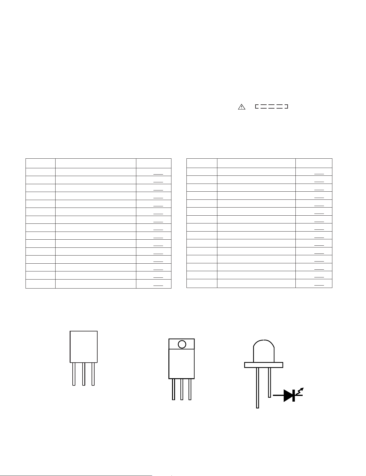
KTA1266 GR
KRC102 M
KRC104 M
KTA1271 Y
KTA1274 Y
KTA1273 Y
KTC3203 Y
KTC3199 GR
KTC107 M
2SC3203 Y
KTC3194 Y
FRONT
VIEW
BCE
KTD2026 Y
Figure 20 TYPES OF TRANSISTOR AND LED
– 16 –
FRONT
VIEW
4204SRT7
4204UYT7
Page 17
CNP12
CNP11
CNP5 CNS99
Q2
+3.3V
+5V
CONT5
CONT2
CONT3
CONT4
CONT7
CONT6
SLD0
SPD0
FD0
TD0
+5V
TO DISPLAY SECTION
CLAMP SW
CDINT
WRQ
CE
DO
CLK
DI
CD RES
GND
DRF
CNS4
BI4
CNP4
M2
SLED
MOTOR
M1
SPINDLE
MOTOR
M
M
TRACKING COIL
FOCUS COIL
PICKUP UNIT
TE
FE
RFEV
HFL
VVDD
ADAVDD
VDD
LVDD
RVDD
XVDD
VDD5V
RFEV
FE-
FE
TE-
TE
HFL
+3.3V
Q1
LDD
PD
TIN2
TIN1
FIN2
FIN1
IC3
M63001FP
FOCUS/TRACKING/
SPIN/SLIDE DRIVER
IC1
LA9235M
SERVO AMP.
TO MAIN SECTION
(TO IC601)
CD DIGITAL OUT
IC99
R-CH
L-CH
AGND
DGND
+B6(+5V)
RCHO
RVSS
LVSS
LCHO
IC2
LC78641E
SERVO/SIGNAL
CONTROL
-
+
M
SW1
OPEN/
CLOSE
XL1
16.9344MHz
6
5
43
3
2
5
4
1
3
21
3
21
12
34
7
8
217
89
10
12
4
3
5
SW2
CLAMP
SW3
DISC
NUMBER
M3
T/T
UP/DOWN
MOTOR
6
12
4
3
56
12
4
3
56
75
DOUT
37
76
45 46
47 48 32 31
30
65
66
67
68
69
70
71
72
CE
CL
DI
DO
INT
WRQ
RES
DEF
52
51
XOUT
XIN
73
5
183644 49 50 7 14 15 16
23
24
25
26
33
3
13
19
40
64
74
17
18 19 20
21
22
30
23
11
9
1
45671516 26 27
2 1725 4142 3839
35
29
22
21
14
8
40
24
23
28
SW4
PICKUP IN
Q3
LASER
DRIVER
CONSTANT
VOLTAGE
+3.3V
+5V
VCC4
18
VCC1
VCC2
VCC3
CD-DP2500W/DK2500W
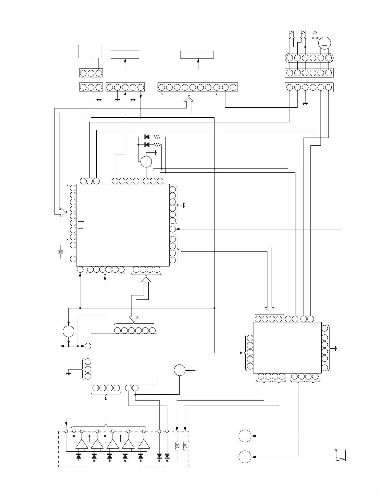
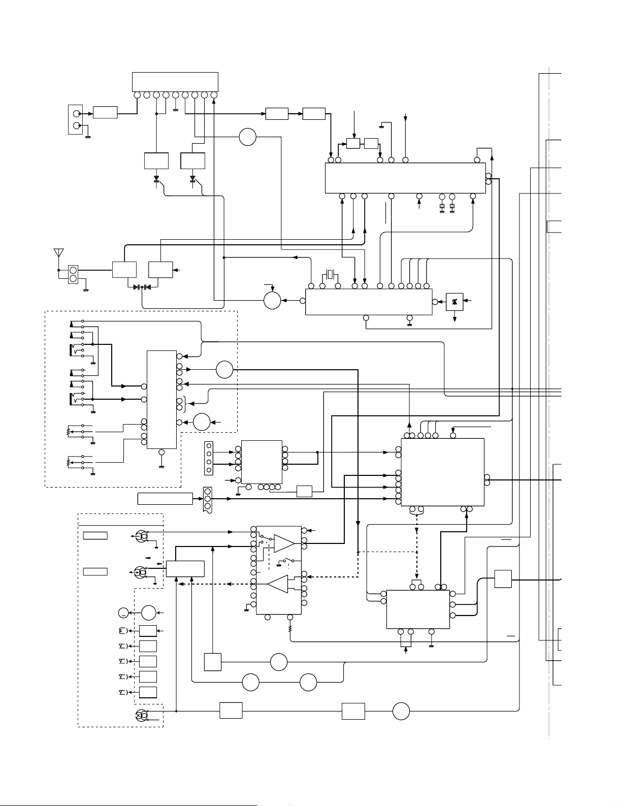
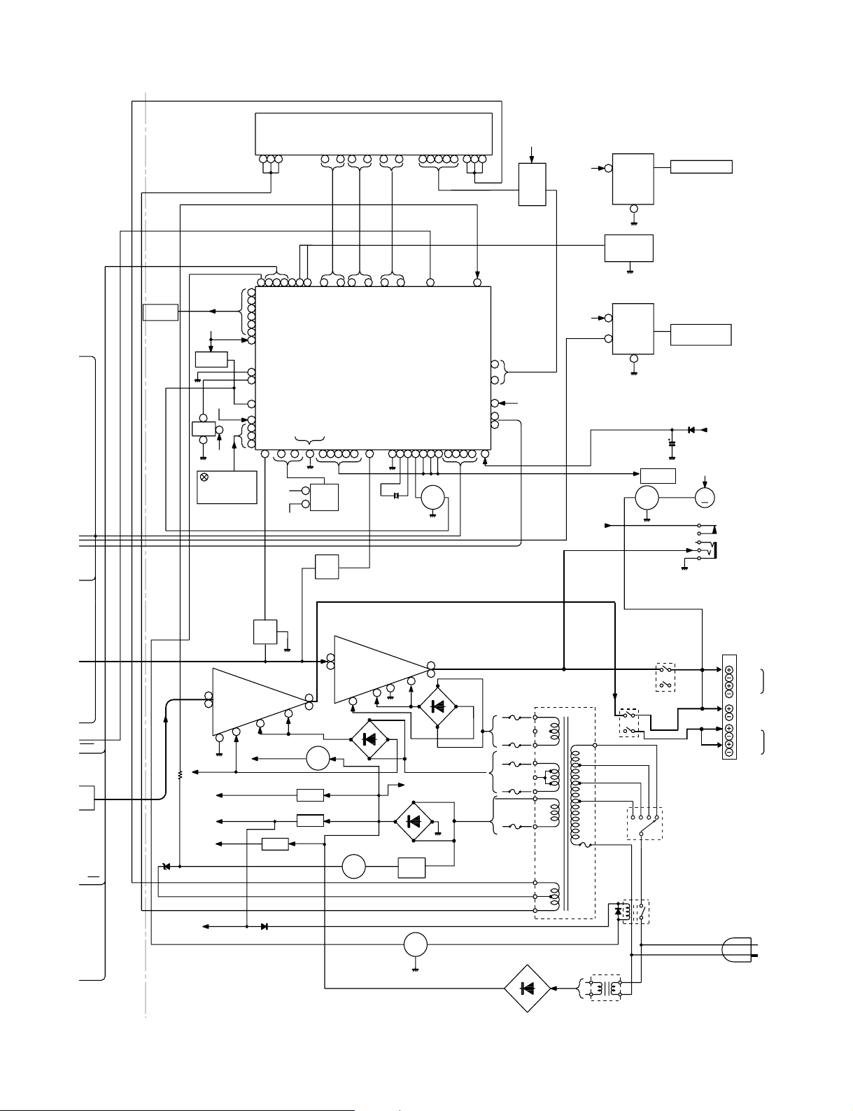
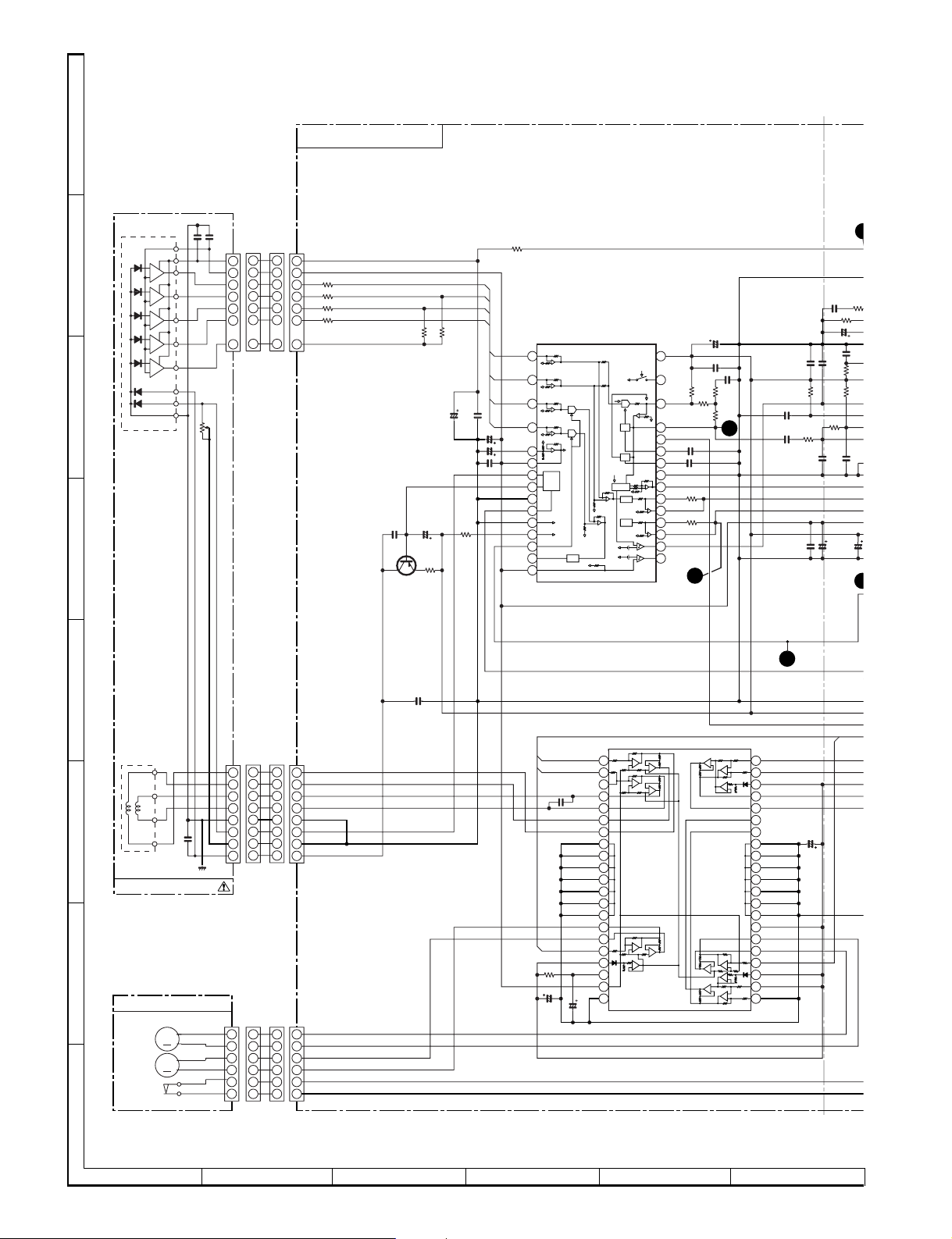
Figure 21 BLOCK DIAGRAM (1/3)
– 17 –
Page 18
CD-DP2500W/DK2500W
D
P
A
IC301
SO301
FM ANTENNA
FM 75Ω
GND
AM LOOP
ANTENNA
BF301
FM B.P.F.
CNP301
AM ANT. AM OSC
1
2
JK1
MIC 1
JK 2
MIC 2
VRK 2
MIC 2
LEVEL
VRK 1
MIC 1
LEVEL
CD-DK2500W ONLY
TAPE MECHANISM Ass'y
TAPE 1
PB HEAD
TAPE 2
REC/PB HEAD
MM1
TAPE
MOTOR
SOLM1,SOLM2
SOLENOID
SWM2
T2 PLAY
SWM1
T1 PLAY
SWM4
R. PLAY
SWM3
F. PLAY
FM FRONT END
1 2 3 4 5 6 7 8 9
L312
T303 T306
ICK1
M65856P
KARAOKE
LATCH
ROUT
LOUT
LIN
4
RIN
9
CLOCK
DATA
7
VCC
8
12
13
22
FROM CD SECTION
CNP11
REC
P.B
AC BIAS
MOTOR
DRIVER
Q706 +B4
Q704
+B4
Q705
IC701
54PIN
IC701
53PIN
IC701
56PIN
IC701
55PIN
L-CH
R-CH
L-CH
R-CH
M
ERASE
HEAD
MIC1 IN
MIC2 IN
FM OSCFM RF
Q103~Q106
T301
+B9
40
35
36
31
32
41
42
QK1
23
JK201
VIDEO IN
SWITCHING
Q302
OSC BUFFER
+B5
FM +B
REGULATOR
QK2,3
IC201
+B5
BU4066BC
L
R
L
R
1
2
3
CNS401
Q107
Q108
BIAS
OCS
SWITCHING
1
3
8
10
+B5
14
PLAYBACK AND RECORD
/PLAYBACK AMP.
L(T1)
1
24
R(T1)
L(T2)
2
23
R(T2)
L NF
3
4
R NF
Q128
L104
L REC
R REC
REF
Q109
6
9
16
14
12
POP REDUCE
SWITCHING SWITCHING
FM IF
T302
Q360
VOLTAGE
6125137
IC101
AN7345K
T1/T2
REC
NOR/
HIGH
15 19
Q111
SWITCHING
2
9
4
11
P.B.
H/N
T1/T2
7
Q403
Q404
13
4
21
7
18
8
17
10
Q110
CF303
FM IF
FM IF IN
20
FM
+B5
PB
L
R
L R REC
L NF
R NF
ALC
+B9
AM IF
T351
1 2
AM MIX
FM/AM IF MPX.
24
23
AM OSC IN
X352
4.5MHz
22
1
OSC
PLL (TUNER)
SWITCHING
Q124
CF352
IC303
LA1832
21
AM RF IN
AM OSC IN
FM IN
AM IN
16
15
IC302
LC72131
10
VIDEO
TAPE
TUNER
CD
+B9
FM+B
9
5
4
GND VCCAM IF
7 9
+B9
STEREO
CE
11
3 94
6
5
21
2417812
L
R
L
R
L
R
L
R
34
IC501
38
M62464AFP
DOLBY PRO LOGIC
DECORD
CLDICE
9
16
10
15
AUDIO PROCESSOR
11
14
12
13
17
8
L
74
R
75
21 69 25
+B5
BAIS
Q126
8
17
FM DET
CF351
DODICL
VOLTAGE
REGURATER
17
+B9
23
IC401
LC75341
2
1
24
9
3
FM/AM
X351
456KHz
7
MO/ST
12
+B5
18
13
MONO/ST
L
14
15
R
R
21
4
L
+B5
REC
Q501
Q502
T1/T2
BAIS
TA
MECH
Z
Figure 22 BLOCK DIAGRAM (2/3)
– 18 –
Page 19
TAPE
MECHANISM
+B7
RESET
IC704
KIA7042P
+B7
1
RX701
3
2
+B7
KEY
SW701~SW713
SW714~SW722
SW728~SW733
CD-DP2500W/DK2500W
FL701
DISPLAY
~~ ~
33
92 7938375554
IC601
4
IC602
8
IC603
KIA4558P
OPE AMP.
14 53
6
100
~
IX0334AW
1 2 3
535247
50
51
53
54
55
56
46
VDD
40
39
36
34
33
32
31
SYSTEM MICROCOMPUTER
AVDD
27
~
30 25
–B1
+B4
78 85
~
IC701
SMUTE
27
80
XL701
32
1624 2625
660
8
Q709
REQ
545556
VDD
LATCH
MIC IN
23
22 21
24
7
15
~
101112132154117181920
9
1
86
91
16
57
58
VDD
+B7
Q701
Q702
Q703
Q710
Q711
Q712
+B7
+B7
18
18
12
IC702
BU2092F
17
VOLUME
VR701
IC703
BU2092F
17
LED711~LED717
LED701~LED710
LED718
~
+B7
+B7
MEMORY
BACK UP
+B6
M
M901
FAN MOTOR
+B3
TO CD
SECTION
Q910
REC
501
502
T1/T2
ZD801
VROAD
+B8
(UNSW+5V)
IC902
L
1
STK40203
15
POWER AMP.
R
–B2
9
13
–B3(–15V)
(A+10V)
+B5
(CD+5V)
+B6
+B2
(SW+5V)
Q401
Q402
+B2
8
+B4(M+10V)
KIA7805AP
AN78L05
IC804
L
7
10
4
R
KIA7810AP
IC802
IC801
Q503
Q504
L
IC901
1
STK40271
15
R
POWER AMP.
Q823
VOLTAGE
REGULATOR
REGULATOR
VOLTAGE
REGULATOR
–B1
9
D802
VOLTAGE
Q804
+B1
JK601
HEADPHONES
FRONT
L-OUT
7
10
R-OUT
4
13
8
D807
~D809
D818
+B3
Q803
D803
~D806
D801
F801
T5A L 250V
F802
T5A L 250V
F803
T4A L 250V
F804
T4A L 250V
F805
T2A L 250V
VF1
VF2
PT801
POWER
TRONSFORMER
(MAIN)
T.F
RL901
230-240V
220V
127V
110V
RL902
VOLTAGE
SELECTOR
RL801
SW801
L-ch
R-ch
Center
Speaker
L-ch
R-ch
SO901
Speaker Terminal
AC POWER
SUPPLY CORD
Front
Speaker
Rear
Speaker
BAIS
D814~D817
Figure 23 BLOCK DIAGRAM (3/3)
– 19 –
PT802
POWER
TRONSFORMER
AC 110/127/220/230-240V,
50/60Hz
Page 20
CD-DP2500W/DK2500W
TDO
9
M
2
8
A
CNS1B
Vcc
7
7
B
Vref
6
6
E
5
5
A
4
4
B
3
3
F
2
2
C
1
1
C
D
CD SERVO PWB-C
CNS1A
7
7
6
6
R51 68K
5
5
R52 68K
4
4
R53 68K
3
3
R54 68K
2
2
1
1
CNP1
R56
68K
+B
C53
47/6.3
0.001
Q3
KTA1266 GR
LASER DRIVER
+B
R50
47
TIN1
FIN1
FIN2
TIN2
R55
68K
FIN1
1
REF
FIN2
2
REF
TIN1
C55
C54
0.01
47/10
C7
10/35
C8
0.022
C51
+B
R25
10K
R47
3.3
TIN2
C6
100/10
REF1
VREF
LDD
GND
LDON
AGON
EFBL
TEST0
TES1
3
REF
4
REF
5
6
7
8
9
10
11
12
13
14
15
REF
APC
ODRV
AGCON
IC1
LA9235M
SERVO AMP.
REF
REF
LPF
REF
C11
47/6.3
VCC
30
ODRV
REF
AGCON
REF
PH
DH
ODRV
PH/BH
REF
LPF
REF
LPF
REF
REF
REF
0.022
RFSW
29
R42
120K
RF-
28
39K
RF
27
NC
26
C13
PH
0.01
25
BH
24
C14
0.33
23
RFEV
22
R3
FE-
21
47K
FE
20
R4
TE-
19
10K
TE
18
HFL
17
16
TEST
C12
6.8K
R5
C18
R7
3P
(CH)
R6
27K
5
C17
0.0047
4
C20
0.1
C82
0.022
C23
R12
0.047
680
R7
1.5
C24
2.2/50
C21
0.1
C22
C25
100P
0.022
R10
27K
330
R11
12K
R80
1M
R15
R8
10K
C42
C26
68P
0.047
C28
47/10
C41
100/6.3
E
F
G
H
FO-
TRTR+
FO+
GND
TR+
FO+
FOTR-
ACTUATOR
PICKUP UNIT(306)
CD MOTOR PWB-D
M1
SPINDLE
MOTOR
M2
SLED
MOTOR
SW4
PICKUP IN
+
M
+
M
-
VR
CNP3A
13
C52
0.01
+B
TDO
TO
FDO
1
2
3
4
5
6
PD
7
8
LD
6
5
4
3
2
1
2
3
4
5
6
7
CNS2B
CNS3B
6
5
4
3
2
1
2
3
4
5
6
7
88
CNS3A
6
5
4
3
2
1
CNS2A
1
TR+
2
FO+
3
FO-
4
GND
5
PD
6
VR
7
LD
8
CNP2
+B
R48
6.8K
100/6.3
SP-
6
SP+
5
SL+
4
SL-
3
PUIN
2
GND(D)
1
CNP3
+B
TR-
1
1
FD
FO
C46
0.022
FO+
FO-
TR+
TR-
GND
SL-
SL+
SLDO
VCC1
STANDBY
Vref
MUTE
C50
C49
100/6.3
-
1
2
3
4
5
6
7
8
9
10
11
12
13
14
15
16
17
18
19
20
21
-
+
+
-
-
+
+
IC3
M63001FP
FOCUS/TRACKING/
-
-
+
+
+
-
SPIN/SLED DRIVER
+B
+
-
-
+
+
-
LD_M+
42
+
LD_M-
-
41
VCC4
+
40
-
LOADING M+
39
LOADING M-
38
37
36
35
34
33
GND
32
31
30
29
VCC3
28
SP-
27
SP+
26
SPO
-
25
+
VCC2(SPN)
+
24
-
23
+
-
22
SPDO
C47
100/6.3
+B
+B
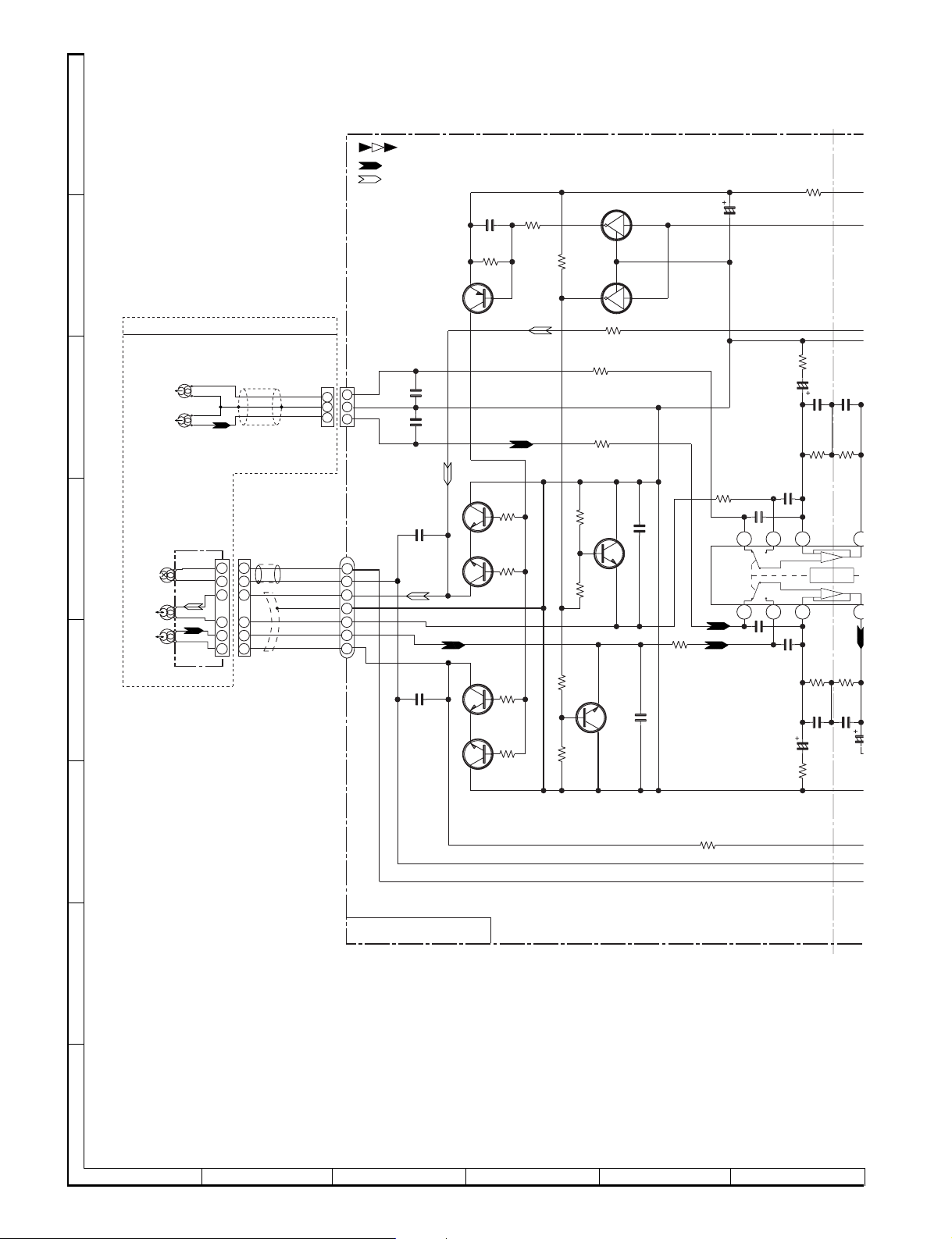
• NOTES ON SCHEMATIC DIAGRAM can be found on page 16.
1
23456
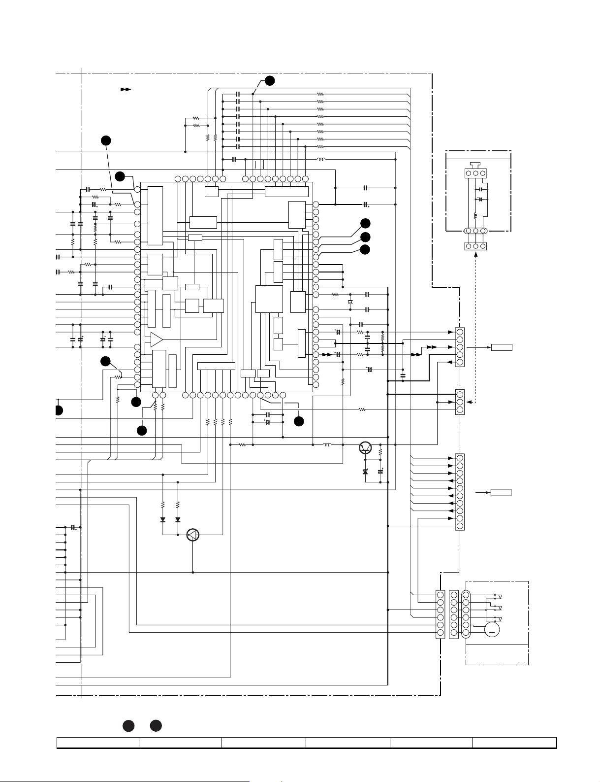
Figure 20 SCHEMATIC DIAGRAM (1/13)
– 20 –
Page 21
CD-DP2500W/DK2500W
N
N
0
CD SIGNAL
R94
10K
R95
JITER
DEFECT
R39
470
EFMO
+B
80
D/A
SLDO
FG(D_Vref)
+B
R22
470
Q2
KRC102 M
10K
DEFECT
79 78
FRAME SYNC
DEFECT,PROTECT
EFM DECODE
CLV
CONTROL
SW
AUTO
ADJUST
LASER
27
28
+B
D22
DS1SS133
1
FSEQ
8
C26
C28
47/10
0.047
R12
680
R79
1.5M
C21
0.1
R11
12K
C27
0.1
PH(RFENV)
2
TDO
R13
680
R44
1K
7
VVSS
C81
0.022
PCKIST
VVDD
R14
1.2K
SLCIST
SLCO
EFMIN
JITTV
JITTC
VREF
ADAVDD
C29
0.022
ADAVSS
PHREF
BHREF
TBLO
R35
1K
FDO
PD01
PD02
HFL
TDO
FDO
1
2
3
PLL
VCEC
4
5
FR
6
7
8
SLICE
LEVEL
9
CONTROL
10
11
CONTROL
12
BH
13
14
FE
TE
1
15
16
17
18
19
20
21
22
23
24
6
SPDO
R38
270
D21
DS1SS133
+
-
25
SPDO
R21
470
A/DSW
S/H
26
SLDO
C23
0.047
C24
2.2/50
C22
C25
100P
0.022
R10
R80
27K
1M
C20
0.1
R15
R8
330
10K
17
047
C42
68P
C82
0.022
C41
100/6.3
3
+B
G M+
G M-
C47
100/6.3
DISC_NO
CONT7
V/vP
77
76
GENERAL
PROCESSEROR
CONT2
CONT1
30
29
R40 1.2K
32
O/C
R67 1K
R68 1K
CONT6
VSS
74
75
SERVO
GENERAL
CONT4
CONT3
32
31
R46 1K
R45 1.2K
C71 100P
C72 0.01
C73 100P
C74 100P
C75 100P
C76 100P
C77 100P
C78 100P
+B
C80
0.022
VDD5V
73
LC78641E
SERVO/SIGNAL
CONTROL
ERROR
CORRECT
CONT5
33
35
34
PCK
R17 1K
R16
10K
C2F
DEF
72
36
VDD
IC2
RES
71
AUDIO
OUT
37
DOUT
INT
WRQ
70
69
INTERPOLATION
MUTE
ATTENUATION
FSX
39
38
C30
0.022
C31
100/6.3
SERIAL
EXTERNAL
DEEMPHASIS
DIGITAL
1BIT
68
67
COMMAND
INTERFACE
OUT
AUDIO IN
FILTER
DAC
EFLG
40
SUBCODE
DECODE
CRC
TEST
CLDIDO
66
CLOCK
GENERATOR
9
R71 1K
R72 1K
R73 1K
R74 1K
R75 1K
R76 1K
R77 1K
R78 1K
CE
65
LPF
+B
64
63
62
61
60
59
58
57
56
55
54
53
52
51
50
49
48
47
46
45
44
43
42
41
2.2µH
L62
SBCK
PW
SBSY
SFSY
16M
DATA
DATACK
LRSY
ASDFIN
ASDACK
ASLRCK
XVSS
XOUT
XIN
XVDD
RVDD
RCHO
RVSS
LVSS
LCHO
LVDD
MUTER
MUTEL
EMPH
0.82µH
L61
R20
220
16.9344MHz
C39
10/16
+B
C44
0.022
C45
100/6.3
12
11
10
XL1
+B
C34
0.022
+B
R82
2.2K
C38
10/16
R81
2.2K
+B
C56
330/6.3
47
R19
+B
R87
120
CONSTANT VOLTAGE
Q1
KTC3203 Y
ZD61
DZ3.9BSB
C35
8.2P
C36
10P
C40
0.0015
C43
0.0015
DRF
RES
WRQ
INT
DO
DI
CL
CE
+B
10K
R84
10K
R83
C83
0.022
+B
220
R58
C64
47/6.3
+B
DIGITAL OUT PWB-A5
R-CH
AGND
L-CH
DGND
+5V
+B
CNP11
CNP5
+B
INT
WRQ
DRF
CE
DO
DI
CL
RES
CNP12
1
2
3
4
5
1
2
3
1
2
3
4
5
6
7
8
9
10
21
3
L99
2.2µH
12
3
CNS99
12
3
CDINT
WRQ
DRF
CE
DO
DI
TO DISPLAY PWB
CLK
CD RES
CLAMP SW
GND
IC 99
C98
0.022
C99
100/10
BI99
P24 5 - H
CNS401
TO MAIN PWB
P29 9 - A
CNS701
3
PDO
PN)
GND(D)
DISC_NO
CNS4
O/C
M+
M-
CNP4
BI4
1
1
1
2
2
2
3
3
3
4
4
4
5665
5
6
SW1
OPEN/
CLOSE
SW2
CLAMP
SW3
DISC
NUMBER
+
M3
M
T/T
-
UP/DOWN
LOADING
CD LOADING
+B
MOTOR PWB-F
• The numbers 1 to 13 are waveform numbers shown in page 43.
7
8 9 10 11 12
Figure 21 SCHEMATIC DIAGRAM (2/13)
– 21 –
Page 22
CD-DP2500W/DK2500W
1
R132
A
B
TAPE MECHANISM ASS'Y(210)
TAPE1
PLAYBACK HEAD
R-CH
C
D
E
L-CH
TAPE2
RECORD/
PLAYBACK HEAD
ERASE
HEAD
R-CH
L-CH
1
2
3
4
5
6
CNS102
1
2
3
4
5
6
TAPE1_R
A_GND
TAPE1_L
CNS101
M_GND
ERASE
TAPE2_R2
A_GND
TAPE2_R1
TAPE2_L1
TAPE2_L2
3
2
1
CNP102
CNP101
3
2
1
1
2
3
4
5
6
7
MIC SIGNAL
PLAYBACK SIGNAL
RECORD SIGNAL
C102
0.001
C101
0.001
C106
180P
C105
180P
C109
0.047
R113
10K
Q109
KTA1266 GR
Q104
2SC1845 F
R104
2.2K
R106
3.3K
Q106
2SC1845 F
Q105
2SC1845 F
R105
3.3K
R103
2.2K
Q103
2SC1845 F
R114
10K
R107
R115
4.7K
R109
47K
R112
15K
R108
R110
4.7K
2
2
47K
4.7K
KRC104 M
3
1
1
3
KRC104 M
R102
1K
R101
1K
C108
Q108
KTC3199 GR
Q107
KTC3199 GR
Q110
Q111
0.001
R117
1K
IC101
AN7345K
PLAYBACK AND
RECORD/
PLAYBACK AMP.
C107
0.001
R118
1K
C153
100/16
C112
330P
24
1
C111
330P
23
47/25
R120
C114
330P
C113
330P
C117
0.033
C115
R174
150
56
C116
47/25
C118
C120
0.033
560P
R122
100K
22
+
Hich=T1
+
-
112K
112K
2
43 2
R121
R123
100K
3.9K
C119
560P
C121
47/25
R119
56
F
MAIN PWB-A1(1/3)
G
H
• NOTES ON SCHEMATIC DIAGRAM can be found on page 16.
1
23456
Figure 22 SCHEMATIC DIAGRAM (3/13)
– 22 –
R111
15K
Page 23

CD-DP2500W/DK2500W
174
50
C124
20
0.022
3.9K
R136
R126
5.6K
6.8K
R138
68K
R134
C132
19
5
6
C127
C123
0.022
0.022
C128
R137
3.3/50
R135
18
7
6.8K
C131
3.9K
R132
5.6K
C116
47/25
C120
118
.033
122
00K
-
Hich=T1
+
-
C122
560P
47/25
R124
3.9K
21
112K
112K 56K
4
121
R123
00K
3.9K
C119
560P
R125
C121
5.6K
47/25
R119
56
R131
5.6K
R182
100K
Q122
KTC3199 GR
R142
1.5K
R140
C136
270P
C134
22/25
17
+ +
Hich=CHROME
+
-
8
C133
22/25
R141
270P
1.5K
R139
100
0.022
56K
100
C135
C140
0.022
R154
10K
0.0033
C142
16
9
R146
47/25
C141
47/25
10K
15
10
R145
Nor/CrO2
ALC
10K
KTC3199 GR
R153
10K
C145
14
RIPPLE
ALC
11
C139
0.0033
22/25
Q121
C146
13
12
220/10
Vcc
GND
R181
100K
R158
220
D102
1SS133
D101
1SS133
Q124
KTA1266 GR
82(1/2W)
C154
0.047
R166
C150
0.0082
R162
R160
22K
47K
R164
4.7K
R167
R168
4.7
47K
3
2
Q128
KTC3203 Y
1
Q126
TAPE_R
T1/T2
REC_MUTE
REC_R
REC_L
TAPE_L
BIAS
D_GND
A_10V
A_GND
KRC104 M
M_GND
11
13
14
15
16
12
17
18
19
20
21
TO MAIN PWB
P25 11- A
L104
330uH
C151
0.039
7
8 9 10 11 12
C152
47/25
Figure 23 SCHEMATIC DIAGRAM (4/13)
– 23 –
Page 24

CD-DP2500W/DK2500W
DGND
1
6
2
/
R
3
R
2
C
4
K
A
B
R503
100K
C545
0.0068
C548
100/50
C547
A_GND
A_GND
REAR
CENTER
CD(+5V)
D_DGN
A10V
M_GND
M10V
220/50
CNP501
1
-15V
2
3
4
5
6
7
8
9
10
11
12
13
C550
10/50
–B
+B
+B
+B
C
D
E
FRONT_R
FRONT_L
CNP805
TO POWER
PWB
P30 1-E
CD GND
F
C540
10/50
0.01
C544
47/50
C546
4.7/50
R502
100K
C549
R504
C543
150K
65
66
67
68
69
70
71
72
73
74
75
76
77
78
79
80
0.01
C501
R507
150K
C542
0.01
R506
47K
R508
150K
64
NGC2
NGC1
AVCC
VREF1
IREF1
LTIN
RTIN
1
2.2/50
R505
ABL
LOUT
C541
150K
63
RBPF1
ROUT
R529
R513
C502
680P
R511
150K
150K
R509
61
62
RBPF2
CVOLOUT
432
C504
10/50
C503
10/50
10K
KTC3199 GR
330
2.2/50
CENTER
R516
C539
R510
LBPF1
65
66
CVOLIN
60
0.01
47K
5
Q501
C551
2.2K
LBPF2
ABR
COUT
0.1
C537
0.1
C535
C533
0.022
C531
0.047
0.1
C536
C534
0.022
58
56
55
57
RLC8
RLC3
RLC7
M62464AFP
DECORDER
PSRIN
PSLIN
10
9
8
7
C505
10/50
C506
10/50
Q502
KTC3199 GR
C552
0.001
REAR
2.2K
R519
C532
54
RLC4
RLC1
IC501
SLOUT
SLVOLIN
SLVOLOUT
11
10K
R518
330
R530
0.1
53
RLC2
SROUT
12
R545
C538
680P
59
RLC6
NGC3
DOLBY PRO LOGIC
SOUT
6
0.001
52
13
C507
+B
C530
RLC5
22K
0.22
C529
0.1
51
PSC4
SRVOLIN
14
1/50
0.22
C528
50
49
PSC1
ECHOOUT
SRVOLOUT
16
15
C569
C527
PSC5
BNR IN
22/50
4.7/50
C526
48
PSC2
DBC1
17
0.22
C525
4.7/50
47
46
PSC6
41
42
43
DSELOUT
CMC
18
19
0.1
C508
DZ5.1BSB
22K
R546
C523
0.68
C524
PSC3
DVSS
AGND
ZD502
0.22
45
C567
+B
44
DBC3
26
25
MICIN
1/50
C568
SR MUTE
C MUTE
R512
C522
DBC2
DVDD
22/50
330K
C521
0.047
43
42
DVOLOUT
LPF2OUT
LPF2IN1
LPF2IN1
DAINTOUT
DAINTIN
DACONT
ADCONT
ADINTOUT
ADINTIN
LPF1OUT
LPF1IN2
LPF1IN1
DATA
23
222120
C509
100/16
SCK
C520
0.0056
1/50
41
DIN
REQ
24
C510
40
39
38
37
36
35
34
33
32
31
30
29
28
27
26
25
0.022
R501
C519
0.001
150
+B
C518
0.0047
C517
0.1
C515
0.22
C514
0.1
C513
0.001
C512
0.0047
C511
1/50
C516
0.22
CD-DK2500W
ONLY
CNP401
OUT(L)
2.2K
R524
Q504
KTC3199 GR
330
FRONT R
R412
R409
100K
CE
22K
TO TUNER
DI
DO
CLK
P27
TUN_SM
Q401
R52
10K
R40
3.9
C4
4.7
654321
A_GND
C
2.
KTC3199 GR
CNSK1
P32 5-A
TO KARAOKE PWB
10 11
+10V(A)
5
OUT(R)
6
IN(R)
7
GND(D)
8
DATA
9
CLOCK
R523
Q503
KTC3199 GR
FRONT L
MIC IN
KARAOKE LATCH
S MUTE
22K
R401
2.2K
C553
C554
0.001
0.001
R521
330
–B
+B
C423
10/50
R520
+B
2
4
3
1
IN(L)
GND(A)
TO TAPE MECHANISM
MIC SIGNAL
CNS100
LUG101
(250)
+B
CD SIGNAL
VIDEO SIGNAL
FM SIGNAL
G
PLAYBACK SIGNAL
RECORD SIGNAL
MAIN PWB-A1(2/3)
H
• NOTES ON SCHEMATIC DIAGRAM can be found on page 16.
1
23456
Figure 24 SCHEMATIC DIAGRAM (5/13)
– 24 –
CNS401
+B
1K
R219
+B
C212
47/16
R220~221
R221
R220
820K
CD_R
5v
A_GND
CD_L
CD_GND
BI401
1
3
2
4
5
1
3
2
4
5
CNP11
TO
CD SERVO PWB
P21 12-D
K
Page 25

CD-DP2500W/DK2500W
4
FC701
CD-DP2500W:23Pin
CD-DK2500W:25Pin
1
TO TUNER SECTION
P27 11-H
654321
H
1
R520
2.2K
R524
Q504
330
FRONT R
CE
DO
KTC3199 GR
22K
R412
R409
100K
DI
CLK
+10V
A_GND
D_GND
TUN_SM
+B
R402
2.2K
Q401
KTC3199 GR
R526
10K
C401
2.2/50
C402
0.1
R404
3.9K
C404
0.0027
C424
4.7/50
C405
1/50
C406
C407
1/50
R403
R525
C403
0.1
C426
2.2/50
1/50
C408
TUNL
1/50
10
987
TUNR
560
10K
10
11
SPAN
SELECTOR
SW799
FM/AN
kHz
KARAOKE LATCH
IC401
LC75341M
AUDIO
PEOCESOR
DI
1
CE
2
VSS
3
LOUT
4
LBASS
5
LTRE
6
LIN
7
LSELO
8
L4
(VIDEO)
9
L3
(TAPE)
L2
(TUNER)
(CD)
50/9100/10
MIC IN
RBASS
RSELO
(VIDEO)
(TAPE)
(TUNER)
(CD)
VREF
ROUT
RTRE
CLK
VDD
RIN
R4
R3
R2
1
24
23
22
21
20
19
18
17
16
15
14
R1L1
1312
2
3
1
2
4
3
5
SPN
M_10V
SW_OUT
C422 1/50
R406 22k
2.2k
R407
KTC3199 GR
560
R408
R528
10K
C421
2.2/50
C417 0.1
C416 0.1
C415 0.0027
C427 2.2/50
C425 4.7/50
C414 1/50
C413 1/50
C411 1/50
C410 1/50
+B
4
6
D_GND
Q402
R527
10K
5
7
M_BUSY
C420
100/16
6
8
S_MUTE
C419
0.022
C418
2.2/50
R405
3.9K
R411
IC201
BU4066BH
7
9
SPEANA0
22K
8
10
SPEANA1
VIDEO2
9
11
SPEANA2
R410
100K
+B
10
11
12
13
SPEANA3
–B
CNP701
14
DO
+B
12
DI
+B
P28 1-E
TO DISPLAY PWB
14
16
15
13
17
16
15
18
CE
CLK
DP_REQ
-20dBATT
+B
17
19
M_GND
19
18
21
20
SR_MUTE
VIDEO2
20
22
23 24 25
REC/PLAY
+B
+B
CNP602
21
T1/T2
+B
22
23
BIAS
C_MUTE
CNP602
CD-DP2500W:23Pin
CD-DK2500W:25Pin
CNP602
TAPE_R
L
11 12
TAPE_L
–B
TO DECK SECTION
P23 12-B
13
141516
T1/T2
REC_L
REC_R
REC/PLAY
R601
33K
R602
12K
R603
470K
R604
47K
IC602
KIA4558P
OPA AMP.
R619
470K
C610
0.022
C611
R620
0.022
470K
C612
0.022
R621
68K
R622
12K
R623
68K
R624
12K
D606
DS1SS133
17 181920 21
BIAS
D_GND
+10V
+B
+B
IC601
KIA4558P
OPA AMP.
C601
270P
C602
270P
2
-
+
3
R605
C603
220K
0.0068
6
-
+
5
R608
D603
2.2M
R606
2.2M
DS1SS133
C609
0.022
2
-
3
+
150K
R617
6
-
5
+
R618
150K
C613
0.0027
C614
0.0027
2
3
R625
220K
6
5
C615
0.0027
220K
R626
C616
0.0027
R607
390K
R615
220K
-
-
+
-
+
A_GND
C604
0.0068
R627
390K
R616
220K
R628
390K
+B
M_GND
D601
DS1SS133
4
1
8
D602
DS1SS133
7
C606
2.2/50
R611
330
-VCC
4
1
C608
0.022
8
7
D604
4
DS1SS133
1
C617
8
2.2/50
7
D605
DS1SS133
2.2/50
IC603
KIA4558P
OPA AMP.
C618
C605
2.2/50
C619
C607
R613
47/25
+VCC
0.022
R612
330
330
SPEANA3
R609
100K
R610
100K
R-CH 1K
R629
100K
L-CH 1K
R630
100K
R614
330
SPEANA2
–B
ZD601
DZ6.2BSC
SPEANA1
–B
+B
SPEANA0
+B
SWITCHING
6
C212
47/16
1K
R219
+B
Q404
KRC107 M
3
23
1
1
Q403
2.2K
R218
R225
330
2
KTC107 M
10K
R217
2
5
9
13
11
12
4
C205
0.022
C206
47/25
IN
CON
CON
IN
CON
IN
IN
CON
14
OUT
1
OUT
8
3
OUT
10
OUT
R215
7
100K
R216
100K
R214
R213
100K
100K
R212
R211
100K
100K
R210
R209
100K
C207
C209
1/50
1/50
100K
C208
1/50
C210
1/50
D202
DS1SS133
D201
DS1SS133
C211
0.022
C201
390P
C203
390P
C202
390P
C204
390P
R205
4.7K
R207
R206
4.7K
R208
4.7K
4.7K
R201
R203
39K
R204
39K
R202
39K
39K
JK201
L
R
L
R
CHASSIS
GND
VIDEO1
IN
VIDEO2
IN
7
8 9 10 11 12
Figure 25 SCHEMATIC DIAGRAM (6/13)
– 25 –
Page 26

CD-DP2500W/DK2500W
2
B
+
3
0
9
I
C
A
C323
0.022
C338 0.001
CHASSIS
GND
B
AM LOOP
ANTENNA
D301 1SS133
D302 1SS133
BF301
B.P.F.
AM BAND
COVERAGE fL
321
5
6
4.7P(CH)
KDV147B
33K
R313
0.001
AM OSC.
C310
15P(CH)
T301
COVERAGE fL
C312
0.022
R327
33
FM BAND
C303
1
1
2
2
CNP301
C
SO301
ANTENNA
FM 75
OHMS
GND
D
D304
E
CHASSIS
GND
1SS133
D303
1SS133
C301
0.022
10P
C304
0.01
C309
FM RF
0.001
4.7P
(CH)
C308
L312
D305 1SS133
R314
22(1/6W)
C315
C314
0.0047
IC301
TA7358AP
FM FRONTEND
4 3 2 1
C305
VD302
R311 100K
C316
0.022
0.0047
C317
F
AM TRACKING fL
T306
7
8
10
R302
18P
C311
R325
47K
OSC BUFFER
AM ANT.
T303
C335
560P(SL)
9
C306
0.022
FM OSC
FM IF
R322
680
Q302
KTC3194 Y
C334
27P
(UJ)
T302
C307
10/16
C324
8.2P(UJ)
C318
100P
C330
15P
(UJ)
R323
68K
VD303
KDV147B
22P(CH)
CF303
FM IF
1
VD301
SVC348S
R309
10K
C313
3
2
C331
0.047
C332
0.022
R316
4.7K
R336
110K
C375
0.001
TP302
C342
0.022
+B
R358
3.9K
R365
10K
24
AM OSC OUT
R351 5.6K
C397
0.022
R382
+B
150 (1/4)
C381
12P(CH)
X352
4.5MHz
C382
15P(CH)
1
C351 0.022
C352 10/16
R381
10K
21
20
22
VSS
AOUT
X OUT
X IN
FM IF IN
C350 0.022
C3
47/1
C39
1/5
L
PLL
CE
321
FM SIGNAL
AM SIGNAL
G
H
• NOTES ON SCHEMATIC DIAGRAM can be found on page 16.
1
23456
Figure 26 SCHEMATIC DIAGRAM (7/13)
– 26 –
R375
470
+B
C384
0.001
R374 1K
+
Page 27
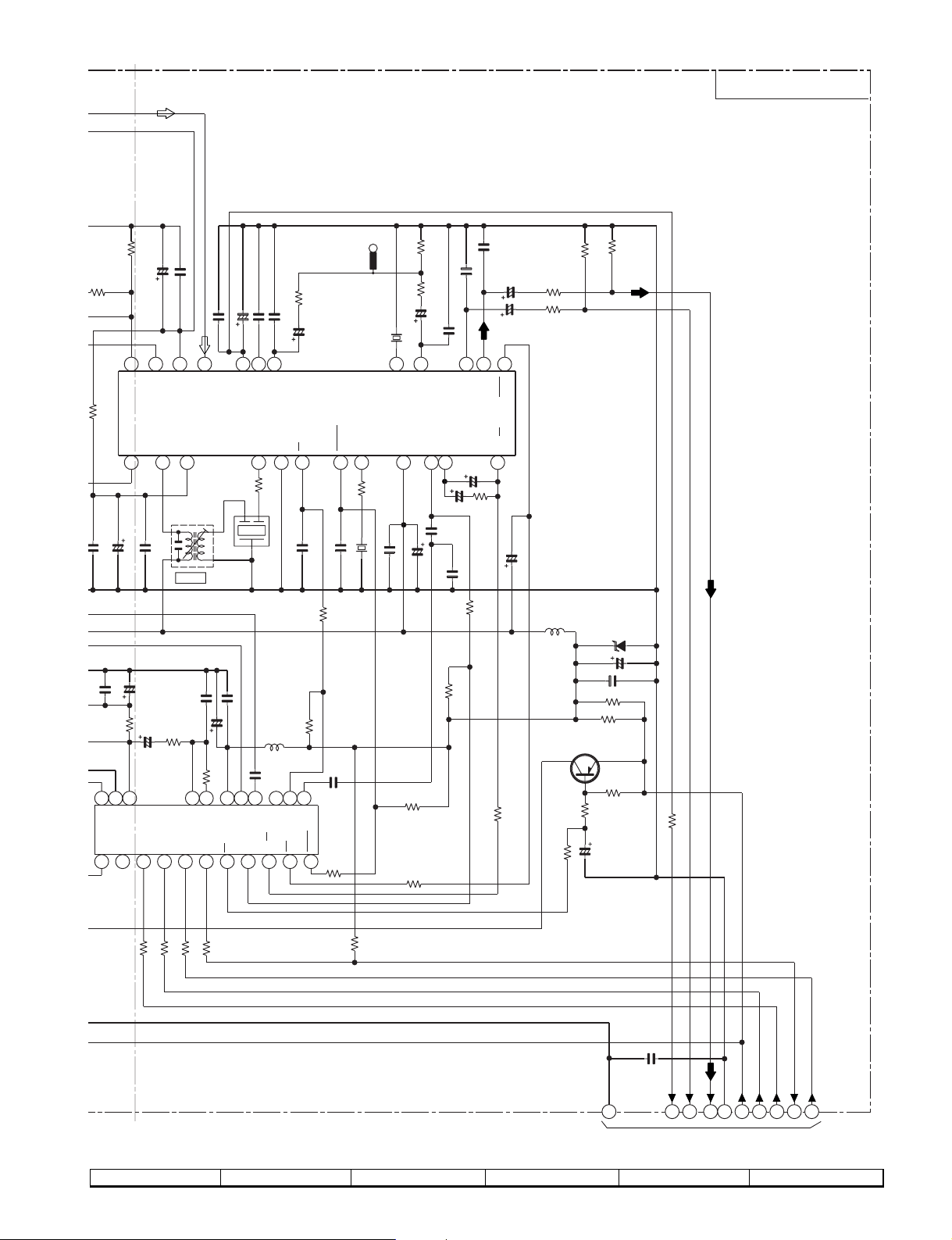
CD-DP2500W/DK2500W
C351
0
022
R351
5
6K
MAIN PWB-A1(3/3)
358
3.9K
.
.
22
X OUT
X IN
R365
10K
24
AM OSC OUT
FM IF IN
C352 10/16
47/16
R381
10K
C393
21
20
VSS
AOUT
PLL (TUNER)
C362 3.3/50
22
23
AM OSC IN
AM MIX OUT
21
C350 0.022
+B
C394
C392
0.001
R380
1.5K
1/50
IC302
LC72131
DI
CE
4
321
C361 0.022
C363 0.022
21
FM AFC
AM RF IN
REG
3
T351
AM IF
C380
10/16
2.2K
R379
19
18
17
PD
AIN
CL
DO
6
5
R350
2.7K
C367
C365 0.022
C364 10/16
20
19
VSM
4
R352
1K
1
2
CF352
AM IF
C387
0.022
15
16
VDD
FM IN
AM IN
CONT
FM/AM
IF
8
7
AM LOW CUT
AM IF IN
3
C385
1/50
C366 0.001
18
FM/AM OUT
FM IF DET/FM MPX/AM IF
GND
SD
6
5
C353 0.022
R377
L351
100µH
0.01
13
12
14
SD
IF IN
MO/ST
ST IND
FM/AM
11
10
9
IC303
LA1832
7
C354 0.022
R393
1K
47K
C386
330P
R376
1K
STEREO
8
CF351
+B
TP302
FM DET
R353
270
FM IF
X351
456KHz
C399
17
0.022
1/50
C368
16
MPX VCO
VCC
9
C398
MPX IN
10
100/10
R395
47K
R360
4.7K
R357
R356
C369
IF OUT
C357
2.2/50
R387
470K
1K
27P
11
C356
0.001
5.6K
15
PHASE
22P
C355
C374
0.015
R-CH OUT
C358
1/50
14
R355
3.3K
C373
0.015
L-CH OUT
PHASE
12
3.9K
R388
R359
C371
1/50
C372
13
1/50
MO/ST
(FM/AM)
1/50
C370
+B
1.8K
R364
3.9K
R361
10K
R362
10K
L352
100µH
+B
SWITCHING
KTA1266 GR
R385
5.6K
5.6K
R384
100/10
R392
Q360
C396
270
C391
47/16
R363
3.9K
ZD351
MTZJ5.1B
C395
0.022
R391
270
+B
R383
5.6K
+B
R370 1K
+B
R373 1K
R374 1K
+B
7
R378 1K
R372 1K
R386
22K
+B
D GND
7
C625
0.022
SM
5
TO MAIN AUDIO SECTION
10
A GND
L
R
9 683 1
P25 7-A
+B
A+10V
CE
DI
CLK
DO
2 4
8 9 10 11 12
Figure 27 SCHEMATIC DIAGRAM (8/13)
– 27 –
Page 28

CD-DP2500W/DK2500W
E
R739
7
C
0
9
3
11
A
B
C
D
E
F
P30 1 - G
CNP804
TO POWER
PWB
P25 9 - A
CNP602
TO MAIN PWB
FC701
CD-DP2500W:23Pin
CD-DK2500W:25Pin
M _10V
SW_5V
VLOAD
SP_DET
AC.RLY-CON
UN SW_5V
SPRLY
CNS702
VF1
VF2
1
BI702
1
1
2
2
3
3
4
4
5
5
6
6
7
7
+B
8
8
9
9
MIC IN
1
2
M_10V
3
1
SPN
4
2
SW_OUT
5
3
D_GND
6
4
M_BUSY
5
7
S_MUTE
8
6
SPEANA0
9
7
SPEANA1
10
8
SPEANA2
11
9
SPEANA3
12
10
DO
13
11
DI
14
12
CLK
15
13
CE
16
14
DP_REQ
17
15
-20dB BATT
18
16
M_GND
19
17
SR_MUTE
20
18
VIDEO2
21
19
T_REC/PLAY
22
20
23
21
24
22
25
23
CNP701
CNP701
+B
+B
T_BIAS
T_T1/T2
+B
C_MUTE
FL701
R718
R716
1K
+B
R714
1K
+B
1K
R719
R728
R735
R743
79
78
77
75
74
73
69
68
67
66
65
63
62
60
57
52
1K
1K
1K
10K
BJ744GNK
83
84
81
82
P5
P4P3P2
80
VLOAD
80
P7
P8
P9
76
P10
P11
P12
P13
72
P14
71
DIST0/P15
70
DIST1/P16
DIST2/P17
DIST3/P18
P19
P20
P21
64
P22
P23
MOVE VOL CTRL SW/P24
61
SPAN/P25
DIS_OUT/SW_OUT
59
KARAOKE LATCH
58
MIC_IN
FPB
56
FPA
55
PLAY SW_B
54
53
51
T1_RUN
SP_DET
SP RELAY
48
49
47
50
R730
1K
R727
R789 10K
1K
R729
4.7K
R788
LED700
4204SRT7
TIMER LED
R744
10K
G11
G12
G13
G14
G15P1P2P3P4P5P6P7P8P9P10
89
87
88
85
P6
90
86
P1
G15
G14
G13
G12
G11
IC701
IX0334AW
SYSTEM
MICROCOMPUT
PLAY SW_A
53
OUT
AC RCY
46
1K
R746
10K
VDD
45
R731
TIMER LED
T_MOTOR
44
43
2.2K
R732
1.8K
R733
T_SOL B
T_SOL A
42
R734
2.2K
C709
SMUTE
41
2.2K
VOLUME
0.001
91
G10
40
VR701
JOG
G10
92
VSS
39
R736
G09
G08
9493
REMOCON
JOY 0
38
37
1K
R737
1K
G07
12
G7G8G9
JOG 1
R738
R
1K
1
F
F
F
P25
P24
P23
P22
P21
P20
P19
D704
DS1SS133
D705
DS1SS133
R721
10K
R720
10K
R722
P18
R724
10K
R723
10K
SW_5V
5554535251504948474443424140393837363534333231302928272625242316151413
56
R701
100K
Q702
KTC3199 GR
Q701
1K
R704
KTC3199 GR
+B
Q710
KTC3199 GR
KARAOKE LATCH
+B
M_GND
R705
Q703
KTC3199 GR
RM710
RM711
100K
100K
RM714
1K
RM713
Q711
KTC3199 GR
D_GND
+B +B
R702
100K
1K
1K
R707
33
R703
100K
R706
C702
47/50
RM712
100K
Q712
KTC3199 GR
1K
1K
RM715
C701
47/50
+B
R709
10K
R712
1K
10K
R745
+B
P13
P11
P12
P14
P15
P16
P17
D702
DS1SS133
D701
DS1SS133
R710
1K
D706
DS1SS133
R713
1K
R715
1K
R717
1K
R725
1K
T2_RUN
CD CLAM SW
R726
10K
10K
+B +B
CNP701
CD-DP2500W:23Pin
CD-DK2500W:25Pin
TAPE MECHANISM ASS'Y(210)
TAPE MECHANISM PWB-E
B
M
SWM2
T2 PLAY
SOLM2
SOLENOID
SOLM1
SOLENOID
SWM4
R.PLAY
SWM1
T1 PLAY
SWM3
F.PLAY
A
+
- -
PH1
PH2
FC702
1
2
3
4
5
6
7
8
9
10
11
12
13
G
MM1
TAPE
MOTOR
H
FC702
• NOTES ON SCHEMATIC DIAGRAM can be found on page 16.
1
23456
Figure 28 SCHEMATIC DIAGRAM (9/13)
CNP702
PLAY SW_B
1
+5V
2
T2_RUN
3
+12V(M)
4
T_SOL B
5
T_SOL A
6
FPB
7
T1_RUN
8
9
PLAY SW_A
10
M_GND
11
12
FPA
13
– 28 –
D718
D717
C708
2.2/50
R783
68K
C707
2.2/50
R786
R784
1K
1K
Q707
R785
KTC3199 G
470K
Q708
R787
KTC3199 G
470K
Q705
+B
Q706
10K
KTA1273 Y
R776
+B
DS1SS133
68K
R782
DS1SS133
R779
R781
10K
10K
Q704
D713
KTA1271
DSISS133
+B
+B
C706
47/25
D714
DS1SS133
KTA1271
Page 29

CD-DP2500W/DK2500W
0
0
7
VDD
P1
P1
TO
R790
47K
FF
1
CD INT
RD07
2
291
WRQ
DS1SS133
KRC102 M
2
1
3.9K
SW707
PLAY
3
354
DRF
Q709
D710
CNP12
5
4
CD_DO
CD_CE
D709
3
DS1SS133
RD08
5.6K
SW708
STOP
6
6
CD_DI
UNSW_5V
+B
C713
3.3/50
R793
7
7
CD_CLK
100K
RD09
10K
SW709
8
8
RES OUT
9
10
10
CD_CLAIM SW
R794
4.7K
IC704
KIA7042AP
RESET
1
3
2
C714
0.022
RD10
15K
SW710
REC
RX701
REMOTE
SENSOR
RD11
33K
SW711
TUNING
UP
UNSW_5V
SW_5V
DS1SS133
DS1SS133
21
RD12
100K
SW712
VIDEO
D711
D712
3
+B
C716
0.022
+B
+B
+B
+B
+B
SW713
TUNER
LED711
LED712
LED713
LED714
LED715
+B
R796
C717
+B
RS701
1K
RS702
1K
RS703
1K
RS704
RS705
1K
IC702 LED DRIVER OUTPUT
Q0
Q1
Q2
Q3
Q4
Q5
Q6
Q7
Q8
Q9
Q10
Q11
IC703
BU2092F
EXPANDER
RS714
LED701
LED702
LED703
RS716
1K
LED704
LED705
+B
IC703 LED DRIVER OUTPUT
Q0
Q1
Q2
Q3
Q4
Q5
Q6
Q7
Q8
Q9
Q10
Q11
100
47/16
1K
1K
RS715
RS717
RS718
1K
DISPLAY PWB-A2
C723
47/16
+B
C724
0.022
1
18
VSS
VDD
17
2
DATA
OE
16
3
CLOCK
Q11
15
4
LCK_0
Q10
14
5
Q0
Q9
13
6
Q1
Q8
12
7
Q2
Q7
RS711
11
8
Q3
Q6
1K
10
Q4
Q5
RS712
1K
LED711
STOP
LED712
PLAY
FF
LED713
LED714
REW
CD DISC1
LED715
CD DISC2
LED716
CD DISC3
LED717
T_BIAS
T_TI/T2
T_REC/PLAY
REV PLAY IND
C725
47/16
C726
0.022
18
1
VSS
VDD
17
2
DATA
OE
16
3
Q11
CLOCK
RS720
15
4
Q10
LCK_1
5
Q0
6
Q1
1K
7
Q2
8
Q3
1K
9
LED701
LED702
LED703
LED704
LED705
LED706
LED707
LED708
LED709
LED710
LED718
14
Q9
13
Q8
12
RS721
Q7
11
Q6
10
Q5Q4
RS722
1K
BYPASS
NORMAL
PHANTOM
CD
TUNER
TAPE
VIDEO
VIDEO2
VOL IND
CMUTE
SRMUTE
REV_PLAY
220
1K
IC702
BU2092F
EXPANDER
RS708
10K
RS709
10K
LED717
LED716
+B
RS723
LED718
1K
LED710
LED708
LED709
LED707
LED706
RS710
10K
+B
+B
RS724
10K
RS725
10K
RS726
10K
CD SERVO PWB
P21 12-F
CNS701
BI701
+B
F
F
99
LCK_1
LCK_0
WRQ
RESET
CD INT
CD_D1
CD_D0
CD_CE
AVSS
32
KEYIN1
R741
G02
100
G2G3G4G5G6G7G8
DRF
X2
X1
VPP
XT2
VDD
CE
CLK
DI
D0
31
1K
KEYIN2
G01
G1
KEYIN2
R748
R749
R750
10K
1
2
3
R772 1K
4
R771 1K
5
R770 1K
6
R769 1K
7
R768 1K
8
R767 1K
9
R766 1K
10
11
XL701
12
13
14
15
16
17
18
19
20
21
22
23
24
25
26
R754
27
28
R752
29
1K
30
R751
1K
R742
10K
10K
SW701
F
C720
47/50
R774
1K
R765 1K
R764 1K
R763 1K
R762 1K
R761 1K
R760 1K
R759 1K
R758 1K
R757 1K
R755
1K
1K
R753
1K
1K
RD01
680
CD
C719
15P
C718
18P
RD02
820
SW702
TAPE
R756
10K
+B
RD03
1K
SW703
TUNING
DOWN
DS1SS133
RD04
1.5K
SW704
MEMORY/
SET
C721
0.022(CH)
220/10
L702
100µH
D708
C711
0.01
C722
RD05
2.2K
SW705
REV
C712
0.1/50
RD06
2.7K
SW706
G11
G10
G09
G08
G07
G06
G05
G04
9493
95
G03
9 8 7 6 3 2 1
98
97
96
-20dBATT
VDD
1
DP_REQ
RES OUT
G12
G13
G14
G15
2625242316151413121110
89
87
88
5
86
G15
G14
G13
IC701
IX0334AW
91
92
90
G9
G10
G11
G12
SYSTEM
MICROCOMPUTER
CD_CLK
SW/P24
VSS
39
REMOCON
38
R737
1K
R736
JOY 0
1K
JOG 1
37
R738
R747
TUN SM/M_BUSY
AVREF
SYS STOP
35
36
10K
R739
1K
10K
C710
0.001
SPEANA3
SPEANA2
SPEANA1
SPEANA0
AVDD
34
33
KEYIN0
1K
R740
PLAY SW_A
53
T_SOL B
TIMER LED
T_SOL A
SMUTE
T_MOTOR
44
6
45
0
T7
ED
46
K
R731
1.8K
R732
43
2.2K
R733
2.2K
42
R734
C709
41
2.2K
VOLUME
0.001
40
VR701
JOG
RD13
RD14
680
SW714
DIMMER
RD18
680
SW720
POWER
820
SW715
X-BASS
RD19
820
SW721
CLOCK
KEYIN1
Q707
85
KTC3199 G
0K
Q708
87
KTC3199 G
K
KEYIN0
RD15
1K
SW716
EQUAL
RD20
1K
SW722
TIMER
RD16
1.5K
SW717
NORMAL
RD21
1.5K
RD17
2.2K
SW718
PHANTOM
RD22
2.2K
RD30
180K
SW719
BY-PASS
RD23
2.7K
SW733
REVERS
RD24
3.9K
RD25
5.6K
RD26
10K
SW728
DISC 1
RD27
15K
SW729
DISC 2
RD28
33K
SW730
DISC 3
RD29
100K
SW731
DISC SKIP
SW732
OPEN/
CLOSE
RS727 1K
RS728 1K
RS729 1K
RS730 1K
RS731 1K
RS732 1K
VIDEO2
C_MUTE
SR MUTE
T_BIAS
T_TI/T2
T_REC/PLAY
7
8 9 10 11 12
Figure 29 SCHEMATIC DIAGRAM (10/13)
– 29 –
Page 30

CD-DP2500W/DK2500W
8
5
4
6
0
1
4
820
DS1SS133
A
+
Front_L
R906
2
3 4 5 6 7 8
1
C901
47P
R901
1K
B
C
C902
15P
R903
56K
R902
C903
47/50
22K
C904
100/50
R905
100(1/4)
R904
1K
C905
820
0.022
R909
6.8K
R921
1/50
C914
FM SIGNAL
IC901
STK40271
POWER AMP.
Out
Ch 1
R988
0.22(2W)
R987
0.22(2W)
R907
0.1
R908
1K
Q901
KTC3199 GR
C915
C916
220P
68K
+Vcc
0.22(2W)
1/50
R989
C906
10/50
D901
DS1SS133
C907
R922
-Vcc
9
10/50
68K
Front_R
Ch 2
Out
C908
11
10
100/50
R910
100
(1/4)
0.22
(2W)
R990
R911
0.1
R912
C909
0.022
R913
6.8K
Q902
KTC3199 GR
220P
C917
IC902
Center
R931
100(1/4)
C938
0.022
68K
STK40203
POWER AMP.
Out
Ch 1
22K
R930
R935
0.1(1W)
R938
10K
Q905
KTC3199 GR
220P
C937
R936
1K
C945
47/50
+Vcc
8
C939
10/50
D904
DS1SS133
9
C940
-Vcc
10/50
Ch 2
10
Rear
Out
11
12
C941
100/50
R942
0.1(1W)
R943
C942
0.022
R944
10K
Q906
KTC3199 GR
Ch 2
13
R941
100
(1/4)
R945
1K
D905
C930
220P
R932
1K
1 2 3
1/50
C935
+
Ch 1
-
4 5 6 7
C931
100/50
15P
R933
56K
R937
820
C933
47/50
C934
220P
R939
68K
1/50
C936
C932
R934
R940
1K
+
Ch 2Ch 1
--
C911
14
13
12
1K
820
R914
D902
DS1SS133
47P
R915
56K
C910
47/50
D903
DS1SS133
Q903
KTC3199 GR
15
C912
R916
15P
1K
1K
R917
Q904
KTC3199 GR
C913
47/50
A_GND
R920
R918
56K
C918
0.1(ML)
C920
0.1(ML)
R923
4.7(1/4)
L
R
56K
56K
R919
C919
0.1(ML)
C921
0.1(ML)
R924
4.7(1/4)
A_GND
A_GND
A_GND
R811
12K
DZ6.2BSA
Q909
KTC3199 GR
R959
47K
C816
2200/50
R810
22K
D803
1N4004S
D804
1N4004S
C823
100/35
ZD801
+B
C987
100/16
D802
3SBA60F
C824
47/50
TS6B0
1N40
1N400
C825
47/50
R812
47K
R813
10
D80
D80
D80
KTA1
Q
D
R958
R801
C803
2200/50
C802
220/25
+B
CONSTANT
VOLTAGE
3
1/50
C805
680
ZD803
DZ130BSB
+B
+B
IC804
AN78L05
1
2
D810
DS1SS133
R802
22K
C833
0.047(ML)
0.1(ML)
CNP805
1
2
3
4
CNS501
FROM
P24 1-F
5
6
7
8
9
10
11
12
13
9
8
7
6
CNP804
E
MAIN PWB
F
5
4
CNS702
3
FROM
PWB
2
1
DISPLAY
P28 2-C
-15V
FRONT_R
A_GND
FRONT_L
A_GND
REAR
CENTER
CD_GND
CD(+5V)
D_GND (micon)
A_10V
M_GND
M_10V
SP_RLY
UNSW_5V
AC_RLY CONT
SP_DETECT
VF2
VF1
VLOAD
SW_5V
M_10V
–B
+B
+B
+B
+B
+B
G
–B
C801
0.022
+B
VF1
VF2
VLOAD
+B
+B
C806
R806
DS1SS133
R808
+B
10K
10K
+B
D811
C811
C804
2200/50
R803
22K
R804
C808
47/16
0.022
22K
C807
C812
47/25
22/25
REGULATOR
C809
0.1(ML)
3
2
KIA7805P
VOLTAGE
REGULATOR
Q823
KTC2026
33
R807
IC802
KIA7810AP
VOLTAGE
3
2
C810
0.1(ML)
1
IC801
1
47K
C815
R809
22K
2200/50
+B
+B
+B
+B
+B+B
+B+B
C813
0.1(ML)
C814
3300/25
POWER PWB-B
H
• NOTES ON SCHEMATIC DIAGRAM can be found on page 16.
1
23456
Figure 30 SCHEMATIC DIAGRAM (11/13)
– 30 –
LUG901(249)
CHASSIS
GND
LUG902(249)
Page 31

CD-DP2500W/DK2500W
C940
HEADPHONES PWB-A3
Rear
-Vcc
Ch 2
10
11
9
C941
100/50
10/50
0.1(1W)
R944
10K
KTC3199 GR
C816
2200/50
R810
22K
D803
1N4004S
D804
1N4004S
C823
100/35
ZD801
DZ6.2BSA
+B
Out
12
R941
100
(1/4)
R942
R943
1K
C942
0.022
Q906
KTC3199 GR
Q909
R959
47K
C987
100/16
TS6B04GM
D802
3SBA60F
1N4004S
R812
47K
R813
10
C824
47/50
+
Ch 2
-
13 14 15
820
R945
DS1SS133
D905
DS1SS133
RL902
R
L
DS1SS133
R991
47K
D801
D806
1N4004S
D805
DZ300BSB
C825
47/50
Q804
KTA1274 Y
C943
220P
R946
56K
R947
1K
D906
Q907
KTC3199 GR
D907
C821
0.047(ML)
C822
0.047
(ML)
ZD802
R814
C944
C946
C826
2.2K
1N4004S
+B
15P
R948
1K
Q908
KT3199 GR
47/50
R952
2.2K
0.1(ML)
C949
0.1(ML)
Q911
KTC3199 GR
0.047(ML)
C818
0.047(ML)
C819
0.047(ML)
C820
0.047(ML)
D807
C827
100/50
220/50
1N4004S
D809
R949
56K
R950
56K
56K
R951
2.2K
R953
+B
+B
C947
R960
4.7
C817
1N4004S
C828
D808
1N4004S
D818
C
R
+B
T5A L 250V
T5A L 250V
T4A L 250V
T4A L 250V
F805
T2A L 250V
220/50
C834
100/50
F801
F802
F803
F804
RL901
C
R
C948
0.1(ML)
C950
0.1(ML)
R961
4.7
R815
1K
+B
2.2K
R956
D908
DS1SS133
R954
+B
330(1/2)
R955
330(1/2)
2.2K
R957
CNP803
CNP802
D812
DS1SS133
R817
220
R816
47K
1
1
2
2
3
3
1
1
2
2
3
3
4
4
5
5
6
6
7
7
8
8
Q803
KTC3199 GR
CNS805
CNS802
C829
1000/6.3
R971
4.7(1/2)
+B
D909
DS1SS133
R972
15K
L901
0.29µH
L902
0.29µH
L903
0.29µH
L904
0.29µH
POWER TRANSFORMER(MAIN)
D814
1N4004S
+B
+B
D817
1N4004S
C830
470/12.5
C961
10/50
PT801
R973
1K
R974
T.F.
133°C
D815
IN4004S
D816
1N4004S
C960
47/50
68K
C986
0.001
D813
DS1SS133
Q910
KTC3203 Y
C832
0.047
POWER TRANSFORMER
CNS907
CNP806
1 1
3 3
5 5
797
CNS806
PT802
(SUB)
1
5
CNS806
121
2
SO901
SP_Rch
+
–
SP_Rch_GND
+
SP_Lch
–
SP_Lch_GND
+
SP_CENTER
–
SP_CENTER_GND
SP_REAR_Loh
+
SP_REAR_Loh_GND
–
SP_REAR_Roh
+
–
SP_REAR_Roh_GND
CHASSIS
GND
CNP806
9
RL801
110V
FAN MOTOR
127V
220V
SW801
VOLTAGE
SELECTOR
M
M901
230-240V
C831
0.0047
FRONT
K801
K801
CNP601
L601
100µH
1
2
3
4
5
6 OHMS
6 OHMS
JK601
HEADPHONES
432
1
5
0.022
C699
C698
0.022
6 OHMS
12 OHMS
12 OHMS
AC POWER
SUPPLY CORD
AC 110/127/220/230-240V 50/60Hz
7
8 9 10 11 12
Figure 31 SCHEMATIC DIAGRAM (12/13)
– 31 –
Page 32

CD-DP2500W/DK2500W
CD-DK2500W ONLY
A
OUT(L)
KARAOKE PWB-G
MIC SIGNAL
RK39
1K
P24 5-A
TO MAIN PWB
CNP401
2 3 4 51
OUT(R)
+10V(A)
GND(A)
IN(L)
2 3 4 51 7 8 96
+B
IN(R)
7 8 96
GND(D)
RK40
1K
DATA
10
CLOCK
LATCH
11
MIC IN
1110
CNSK1
BIK1
+B
B
CK73
2.2/50
RK41
1.5K
RK43
RK44
470K
RK42
1.5K
C
470K
RK48
680
QK2
KTC199GR
RK46
1K
QK3
KTC3199GR
RK45
1K
CK74
2.2/25
RK37
RK36
1K
1K
RK14
+B
100
RK47
680
RK38
100
RK15
CK44
47/25
ZDK1
MTZJ5.6B
100
CK72
100/16
RK13
1.2K
QK1
KTC3203Y
RK12
D
+B
CK34
1K
RK11
RK10 1K
DATA
CLOCK
47P
RK9 1K
LATCH
CK33
PS2
47P
CK31 0.15
CK29 2.2/50
PS1
VCFIL
CK30 2.2/50
35 31
LOUT
ROUT
KEYCONIN
SOURCEOUT
CK25 2.2/50
CK24 2.2/50
CK26 2.2/50
29 26323334
303738393642 41 40
LIN
RIN
VOLIN
CK23 0.001
28
LPF2OUT
LPF2IN2
E
CK35
47P
+B
CK20 0.22
CK21
CK22 0.0047
0.068(ML)
24
2527
DAINTOUT
DACONT
LPF2IN1
DAINTIN
100
CK43
47/25
CK42
0.022
CK41
47/25
CK19
+B
0.022
CK18
100/16
2223
VCC
GND
ICK1
F
G
RK6
5.6K
RK8
5.6K
+B
M65856SP
RK1
10K
RK2
56K
RK3
56K
MCLKCONT
MICSW
2 3 4 51 7 8 96
RK4
CK1
0.01
VALC
CK2 0.47
22K
RK5
1K
ALC1
MIC1NFIN
MIC1IN
CK3 4.7/50
CK4 2.2/50
CK5 0.1
MIC1VOLIN
MIC2IN
MIC1OUT
ALC2
10 16
CK8 4.7/50
CK6 0.1
CK7 0.47
RK7
1K
MIC2VOLIN
MIC2OUT
MIC2NFIN
121314
CK9 2.2/50
CK11 0.1
CK12 2.2/50
CK10 0.1
LPF2IN2
LPF1OUT
LPF1IN1
MICOUT
1511 171819
CK14
0.001
CK13
0.0047
ADINTOUT
ADINTIN
CK15
0.068(ML)
ADCONT
20 21
CK16
0.22
REF
CK17
220/10
DK2
1SS133
CHASSIS
GND
1SS133
JK2
MIC2
DK1
PINK1
H
• NOTES ON SCHEMATIC DIAGRAM can be found on page 16.
1
23456
Figure 32 SCHEMATIC DIAGRAM (13/13)
JK1
MIC1
– 32 –
VRK2
20K(B)
MIC 2
LEVEL
VRK1
20K(B)
MIC 1
LEVEL
Page 33

CD-DP2500W/DK2500W
A
CD-DK2500W ONLY
JK1
MIC 1
JK2
MIC 2
VRK1
MIC 1
LEVEL
VRK2
MIC 2
LEVEL
B
CK6
CK22
CK18
CK5
CK16
CK17
CK21
CK19
CK20
CK26
CK8
CK24
CK25
CK9
CK11
CK12
25303540
CK23
CK10
21
22
CK13
CK14
CK15
RK1
CK35
RK10
CK42
CK44
RK14
CK3
E
C
B
RK15
RK6
1
RK11
42
QK1
CK43
RK40
CK4
5101520
ICK1
CK32
CK31
CK29
CK30
RK36
RK3
CK41
CK7
CK1
RK9
RK5
CK2
RK2
CK34
C
DK1
DK2
PINK1
RK7
RK8
RK4
D
RK44
RK42
RK46
CK33
RK12
ZDK1
RK13
TO CHASSIS
E
RK48
E
C
B
QK2
F
CK74
G
BIK1
RK41
CK72
1011
RK38
111
123456789
CNSK1
RK47
RK45
RK39
RK43
E C B
QK3
CK73
RK37
KARAOKE PWB-G
CNP601
TO MAIN PWB
P35 8-C
H
1
23456
Figure 33 WIRING SIDE OF P.W.BOARD (1/9)
– 33 –
Page 34

CD-DP2500W/DK2500W
2
D
A
B
C
D
E
F
G
ANTENNA
ANTENNA
VIDEO 1
IN
VIDEO 2
IN
75 OHMS
1
2
AM LOOP
R-CH
L-CH
R-CH
L-CH
SO301
ANTENNA
FM
GND
50/ 9
FM/AM
KHz
100/10
JK201
MAIN PWB-A1
CHASSIS
GND
D304
D303
C301
C394
C307
IC301
C306
1
2
CNP301
CHASSIS
GND
SW799
SPAN
SELECTOR
C204
R206
C202
C203
R207
C201
R205
D302
R208
R203
R201
D301
C338
R202
C304
123
BF301
R204
C206
C305
C303
C323
T303
C331
R209
R210
C207
1234567
IC201
C210
R215
C205
R216
9
8
7
6
5
4
3
2
1
C209
C381
C397
R381
C330
R214
1011121314
R212
C384
R314
C315
C314
C316
R213
R211
C382
R322
R302
C310
R323
VD301
89
C208
X352
123456789
C392
C380
C393
C375
TP301
BCE
R325
R327
C312
C308
C309
L312
D305
R316
C334
R336
C332
C335
R225
R218
R217
123
123
C211
R374
R379
T302
VD302
C317
T306
D202
D201
R373
R380
C313
R313
C362
C518
C525
C527
Q403
Q404
R372
IC302
16171819202122
R377
Q302
C311
CF303
1
C528
C318
C324
R309
23
C523
C521
C522
R512
C531
C532
C387
C385
R382
T301
R365
C342
C516
C524
C534
C533
R378
R359
1011
C386
R360
12131415
L351
R375
R393
CF352
3
2
1
C351
VD303
C352
C350
R352
123456789
R311
R358
C367
R350
C361
C364
C363
C515
C512
C517
C519
C520
C526
C529
C530
C535
C536
C538
R387
R383
IC303
R351
C365
C514
41
Q360
R370
TP302
C513
40
C540
R386
B
C
E
C354
C353
C366
C369
C511
R388
R376
R384
T351
CF351
1011 12
C399
ZD502
35
45
50
R510
C537
C391
R385
C398
1415161718192021222324
R357
C510
25
30
R508
C539
C395
R392
55
R353
13
R356
IC501
64 65
R509
R511
C357
C509
24
20
60
C542
R391
R355
C371
15
R506
R507
R395
C370
C356
R361
X351
C368
C567
10
70
C541
C396
ZD351
C355
C372
75
P33 2-G
TO KALAOKE PWB
CD-DK2500W ONLY
CNSK1
R364
R362
1
80
C549
C543
C212
C507
C504
C501
R502
C548
R503
C544
L352
C358
5
R504
R363
C373
C374
R501
C508
C506
R505
R219
C625
C547
C550
C545
C505
C503
C502
C546
P40
TO C
C421
CN
C4
R41
H
1
23456
Figure 34 WIRING SIDE OF P.W.BOARD (2/9)
– 34 –
Page 35

C543
4
33 2-G
LAOKE PWB
2500W ONLY
CNSK1
C212
R364
3
362
1
C507
C504
C501
0
C549
R502
C548
R503
C544
R219
C625
C547
C550
C545
C505
C503
C502
C546
P40 4 - A
TO CD PWB
CNP11
C421
C427
R410
R412
C411
CNP401
CD-DK2500W ONLY
11
10
9
8
7
6
5
4
3
2
1
R406
B
Q402
C
R527
R408
R528
R403
C418
C417
C416
R405
C415
C425
R411
C426
C414
TO TAPE2 RECORD/
PLAYBACK HEAD
5
4
3
2
1
CNS401
R220
R221
R518
R407
R402
B
C
E
Q401
R525
C420
C419
24
23
22
21
20
19
18
17
16
15
14
13
C410
P41 11 - D
GY
WH
GY
WH
RD
R517
R545
R519
Q502
Q504
C422
Q503
B
C
E
C408
1
5
GY
WH
1
BI401
GY
WH
RD
25
24
23
22
21
20
19
18
17
16
15
14
13
12
11
10
9
8
7
6
5
4
3
2
1
CNP602
C568
R546
R401
C569
B
C
E
C552
R516
R529
Q501
C551
R524
B
C
E
R523
B
C
C554
EE
R520
C553
R521
R526
C401
R404
1
2
3
4
5
6
7
8
9
10
IC401
11
12
C404
C403
C406
C402
C424
R409
C405
C407
C413
R182
R181
TO TAPE1 PLAYBACK HEAD
CNS102
P37 10-G
TO DISPLAY PWB
CNP701
CNP602
CD-DP-2500W:23Pin
CD-DK-2500W:25Pin
23
1
C423
R513
R530
1 2345678910111213
CNP501
CE
R135
C123
C121
R139
R131
C131
C128
C115
C135
C127
R119
Q121
R125
R123
C119
R121
R153
B
C117
Q107
C102
3
2
1
CNP101
C101
Q111
321
321
C153
Q110
R114
CNS101
P41 9-D
1
WH
2
3
4
5
6
BR
BK
PK
WH
GY
GR
BL
FC701
CD-DP-2500W:23Pin
CD-DK-2500W:25Pin
R620
R619
R613
R145
R154
D101
C145
C141
C139
R141
C133
12
11
10
9
8
R137
7
6
5
4
3
2
C111
1
C113
R101
R102
C107
R117
Q108
E
E
C
C
B
B
R110
R107
R115
R113
C109
R108
CNP102
E
Q109
R174
WH
BK
PK
BK
WH
GR
BL
R109
C606
R614
D102
C147
IC101
7
R118
C108
CB
C605
C617
C146
13
14
15
16
17
18
19
20
21
22
23
24
R120
C105
1
23
25
R610
R629
R158
C142
Q105
D603
C134
C114
Q103
R603
R609
R623
C618
R630
C611
R618
C612
C619
C607
Q122
BCE
R142
R134
C112
ECB
Q104
ECB
R111
C152
C106
C150
C151
R605
D605
R626
D606
C608
R140
C136
R146
C140
R138
C132
C116
ECB
ECB
Q106
L104
1
23
Q126
CD-DP2500W/DK2500W
C604
R604
C603
D602
5678
R608
R606
R607
C616
C615
5678
R625
R624
ZD601
R616
5678
IC602
C610
R617
R132
R136
C122
R122
C118
R103
R104
R112
R106
C154
R167
ECB
R168
C602
R601
34
C614
R621
C124
R126
R105
R164
D601
R628
R627
2
1234
C609
C120
B
C
E
Q124
R162
1234
C601
R602
1
C613
R612
R611
LUG101
(250)
R124
R166
Q128
IC601
IC603
D604
R622
R615
R160
TO TAPE MECHANISM
CNS100
P38 3 - A
TO POWER PWB
CNP805
COLOR TABLE
BR
RD(R)
OR
YL
GR
BL
VL
GY
WH(W)
BK
PK
BROWN
RED
ORANGE
YELLOW
GREEN
BLUE
VIOLET
GRAY
WHITE
BLACK
PINK
7
8 9 10 11 12
Figure 35 WIRING SIDE OF P.W.BOARD (3/9)
– 35 –
Page 36

CD-DP2500W/DK2500W
S
L
A
C720
SW714
DIMMER
LED710
9
1
BI702
D718
R743
SW732
OPEN/
CLOS
C701
C723
C724
R745
R744
R786
R787
DISC3
SW730
BCE
R785
R784
D717
CNP702
C702
RS720
LED708
R747
R746
C710
VR701
VOLUME JOG
C708
LED717
Q708
CB
E
RD27
Q707
SW729
C707
D713
R722
R783
1
R720
R703
Q702
RS726
RS724
C726
C725
R782
B
C
DISC2
E
Q704
D714
2345678
E
C
B
R707
C709
RS705
LED716
RD26
B
Q705
C
E
RD28
RD29
9
R701
R702
Q701
RS725
LED709
1
9
SW728
DISC1
101112
B
C
CNS702
GY
9
WH
8
GY
7
WH
6
D
CNP804
P38 3 - G
TO POWER PWB
GY
5
WH
4
GY
3
WH
2
RD
1
COLOR TABLE
E
RD(R)
F
WH(W)
BR
OR
YL
GR
BL
VL
GY
BK
PK
BROWN
RED
ORANGE
YELLOW
GREEN
BLUE
VIOLET
GRAY
WHITE
BLACK
PINK
G
DISPLAY PWB-A2
E
C
B
Q703
10
18
5
R776
R779
C706
13
Q712
BCE
15
IC702
RS711
R781
Q706
R721
RM712
E
C
B
Q711
5
IC703
15
18
10
LED715
B
C
E
R725
SW731
RS708
RM711
E
E
C
C
B
B
Q710
9
RS718
RS716
1
RS709
RS710
RS701
RS702
RS712
RS730
DISC SKIP
RM710
RS714
RS717
RS731
RD13
RS715
RS723
RS704
RS703
RS732
R774
RS727
R772
R771
LED703
SW716
EQUAL
SW715
X-BASS
9876321
R770
R769
R767
SW718
PHANTOM
RD14
R768
RS729
R766
RS728
R764
R765
RD07
R762
R761
R763
R760
SW717
NORMAL
RD15
RS721
RM713
RM714
R759
R758
LED701LED702
RD17RD16
SW706
FF
RS722
SW707
PLAY
2625242316151413121110
R704
RM715
R756
R757
LED713
LED712
SW733
RIVERS
R705
R788
SW71
BYPA
F
R706
R729
1
FC702
P41 10 - B
TO TAPE MECHANISM PWB
13
H
1
23456
Figure 36 WIRING SIDE OF P.W.BOARD (4/9)
– 36 –
Page 37

RS722
R759
P40 5 - A
TO CD SERVO PWB
CNP12
CD-DP2500W/DK2500W
RM714
R758
LED701
L
RD17
W706
FF
W707
PLAY
R704
RM715
R756
R757
BYPASS
LED713
LED712
SW733
RIVERS
FL701
R706
R705
R788
SW719
R729
XL701
RD24
RD25
RD30
LED718
SW705
C718
RD06
100
C719
R755
RD09
RD05
RD08
1
C721
R754
SW705
LED711
SW708
STOP
R753
REV
81
90
95
5
10
15
R752
R751
LED714
85
IC701
20
R742
SW709
80
75
25
30
PLAY
70
35
31
RD23
CNS701
WHGYWHGYWHGYWHGYWH
R726
56555453525150494847444342414039383736353433323130292827262524
C716
C722
LED700
C717
RX701
REMOTE
123
SENSOR
R723
R724
R739
D704
R709
D702
R710
D701
D705
R713
65
60
51
55
45
40
R741
50
R738
R740
R718
R737
D706
R734
R728
R733
RD21
R732
R730
R789
R727
L702
R719
RD20
R796
C714
R731
R712
D711
C712
R736
SW722
TIMER
R717
R716
1102345678910
RD
1
D712
R715
BI701
D709
R790
C713
R714
D710
D708
C711
R793
IC704
1
R794
2
3
SW720
POWER
R748
123
Q709
RD19
RD18
SW721
CLOCK
R749
R750
LED705
RD22
LED704
SW701
CD
LED706
RD01
SW702
TAPE
SW704
MEMORY/
SET
RD04
RD03
RD10
SW713
TUNER
SW712
VIDEO
RD12
LED707
RD11
SW710
REC
R735
SW711
RD02
TUNING
UP
SW703
TUNING
DOWN
FC701
CD-DP-2500W:23Pin
CD-DK-2500W:25Pin
CNP701
468101214161820222524
23
CNP701
2
CD-DP-2500W:23Pin
CD-DK-2500W:25Pin
357911131517192123
1
1
1
CNP602
P35 10 - A
TO MAIN PWB
7
8 9 10 11 12
Figure 37 WIRING SIDE OF P.W.BOARD (5/9)
– 37 –
Page 38

CD-DP2500W/DK2500W
L
P35 10 - D
TO MAIN PWB
CNS501
A
CNP805
C801
B
ZD803
R801
C
D
CHASSIS
GND
LUG902
( 249 )
Q905
D904
C802
C961
C938
Q908
R938
B
B
C
E
R973
R974
R932
CE
E
C
B
10111213
D909
R972
R933
C930
R936
D906
B
C
E
R937
Q907
Q910
C931
R934
C932
C946
R949
C935
C933
R939
R930
C934
R931
R935
123456789
R951
C937
R945
IC902
C939
C936
C945
C943
5
CNS907
1
R940
R946
R948
987654321
C940
R971
R955
R954
C944
R941
R950
R947
C941
D905
C949
151413121110
E
C
B
Q906
C947
R944
C942
R943
R960
R942
C948
C950
C915
R921
R961
RL901
C914
R901
Q901
C903
R902
R903
R909
B
C
Q904
E
R920
C902
C901
C905
D903
BCE
E
C
B
Q903
D901
R987
C917
R922
C910
R988
C904
R908
D908
R917
C913
R915
R906
R904
C916
R914
C911
R905
R907
C912
IC901
987654321
C906
R916
R910
C907
R
C987
151413121110
R
R918
E
F
R804
G
CHASSIS
GND
H
POWER PWB-B
R806
C809
C810
C808
R807
IC802
3
2
1
IC801
3
2
1
C807
Q823
E
C
B
LUG901
( 249 )
R808
C811
C813
D810
C833
1 2 3
C812
C806
C805
IC804
C814
D811
C826
D804
D803
C822
C821
D808
C828
R811
12345678 9
P36 1 - D
DISPLAY PWB
C815
D805
D806
CNP804
CNS702
TO
F805
T2A L 250V
C827
D807
C823
C824
ZD801
C816
C834
D809
D818
R814
Q804
ZD802
ECB
R813
R812
87654321
R809
C825
CNP802
D802
C819
CNP803
C820
F803
T4A L 250V
3
2
1
R810
R802
F804
T4A L 250V
C818
R817
R815
C804
D801
R803
F802
T5A L 250V
C829
D812
R816
BCE
C817
Q803
C803
D813
F801
T5A L 250V
C832
D814
D815
D816
D817
C830
1
23456
Figure 38 WIRING SIDE OF P.W.BOARD (6/9)
– 38 –
Page 39

CHASSIS
GND
CD-DP2500W/DK2500W
5432 1
CNP601
16
1
R910
803
F801
T5A L 250V
C832
30
C987
C907
RL902
15141312110
R989
C908
R918
D813
Q911
EB
R991
CEC
B
Q909
R959
R919
E
C
R990
B
D902
C909
Q902
RL801
C831
K801(256) K802(256)
BROWN BLUE
R956
R952
R953
D907
R912
R913
R958
AC POWER
SUPPLY CORD(247)
AC110/127/220/230-240V
50/60Hz
C986
R983
R982
C920
R981
R984
R923
PT802
(SUB)
CNP801
R957
C919
R924
C921
R911
C918
POWER TRANSFORMER
SO901
SPEAKER
TERMINAL
–
REAR
L904
L903
L902
L901
L-CH
+
–
REAR
R-CH
+
–
CENTER
+
–
FRONT
L-CH
+
–
FRONT
R-CH
+
C698
C699
L601
JK601
HEADPHONES
HEADPHONES
PWB-A3
M901
FAN MOTOR
COLOR TABLE
C960
CNP806
1
2
CHASSIS
GND
SW801
VOLTAGE SELECTOR
220V
1
3
230-240V
5
7
9
127V
110V
1
2
CNS806
RD
BR
CNS802
CNS804
POWER TRANSFORMER
BR
1
BK
2
BR
3
OR
4
OR
5
RD
6
BL
7
RD
8
WH
3
BK
2
WH
1
WH(W)
PT801
(MAIN)
BR
RD(R)
OR
YL
GR
BL
VL
GY
BK
PK
BROWN
RED
ORANGE
YELLOW
GREEN
BLUE
VIOLET
GRAY
WHITE
BLACK
PINK
RD
BR
WH
OR
BL
CNS801
1
3
5
7
9
7
8 9 10 11 12
Figure 39 WIRING SIDE OF P.W.BOARD (7/9)
– 39 –
Page 40

CD-DP2500W/DK2500W
P37 11 - A
TO DISPLAY PWB
CNS701
CD SERVO PWB-C
TO MAIN PWB
5
P35 8 - A
CNS401
A
R47
C53
ECB
Q3
C7
CNP2
C8
C55
C54
R53
R52
R56
40
35
30
IC3
25
C50
C51
1
5
10
15 16
C6
R51
R54
42
C47
CNP3
R25
IC1
C44
30
25
20
R4
R44
R17
R16
C52
8
7
6
5
4
R50
3
2
1
7
6
5
4
3
2
1
CNP1
R55
B
13
4
C
2
1
5
C46
10
D
C49
21 22
R48
15
20
C45
C83
12 4531 122453367 9108
CNP11
R42
R5
R6
C14
C13
R3
C28
R35
R39
123
Q2
R7
C18
C26
C27
D21
D22
R46
R8
C29
C20
C41
R22
C11
C17
R10
R38
R21
R58
C22
C42
R15
C82
R40
C12
R45
R95
BCE
Q1
R14
24
25
C31
R94
123456123456
CNP4
C64
ZD61
R80
20
C25
R11
C81
30
C30
15
CNP12
L62
C21
10
35
40 41
R87
C56
R19
R13
R79
IC2
45
CNP5
R78
R71
R74
R77
R75
R73
R76
R72
C73
C76
C74
C80
C75
65
64
R20
C34
L61
R82
C77
C36
C40
C72
R67
R68
XL1
R84
8
7
3
12
11
C35
10
C71
C78
C24
R12
C23
1
80
5
75
70
60
55
50
C38
9
C39
R81
R83
C43
E
CNS99
3
2
1
CNS1A
WH
PK
BK
RD
1
WH
2
BK
3
WH
4
PK
5
YL
6
BL
7
1
2
3
4
5
6
7
8
RD
WH
GY
WH
GY
WH
GY
WH
GY
3
1
BI99
F
G
H
1 6
CNS1B
RD
1
WH
2
BL
3
PK
4
WH
5
YL
6
BK
7
1
2
3
4
5
6
7
8
CNS2BCNS2A
L99
C98
C99
3
2
1
PICKUP UNIT(306)
17
8
1
DIGITAL OUT
PWB-A5
IC99
CNS3A
CNS3B
-
6
WH
6
6
CNP3A
PICKUP IN
+
GR
SW4
12345
RD
GR
WH
WH
12345
CD MOTOR
PWB-D
12345
-
M1
SPINDLE MOTOR
M2
SLED MOTOR
+
• The numbers 1 to 13 are waveform numbers shown in page 43.
1
23456
Figure 40 WIRING SIDE OF P.W.BOARD (8/9)
– 40 –
Page 41

CD-DP2500W/DK2500W
TAPE MECHANISM
ASSEMBLY(210)
TAPE MECHANISM PWB-E
SW
PH
SOLM
SOLENOIDE
MM1
TAPE MOTOR
PLAYBACK HEAD
PK
SW
B
A
+
-
TAPE 1
BK
WH
P36 3 - G
TO DISPLAY PWB
CNP702
FC702
13
13
101112
1
GY
4
1
3
56789
1
2
4
SW
ERASE HEAD
PH
SOLM
SOLENOIDE
TAPE 2
RECORD/PLAYBACK
HEAD
BK
WH
SW3
DISC
NUMBER
456
WH
BI4
BK
WH
123
RD
CNS4
16
+
M3
T/T UP/DOWN
MOTOR
BK
PK
WH
CNS101
1
2
3
CNP101
TO MAIN PWB
P35 9 - F
CD LOADING MOTOR
PWB-F
–
SW1
OPEN/
CLOSE
SW2
CLAMP
654321
CNS102
P35 9 - H
TO MAIN PWB
RD(R)
WH(W)
COLOR TABLE
BROWN
BR
RED
ORANGE
OR
YELLOW
YL
GREEN
GR
BL
VL
GY
BLUE
VIOLET
GRAY
WHITE
BLACK
BK
PK
PINK
7
8 9 10 11 12
Figure 41 WIRING SIDE OF P.W.BOARD (9/9)
– 41 –
Page 42

CD-DP2500W/DK2500W
VOLTAGE
PIN
NO.
10
11
12
13
14
15
16
17
18
19
20
21
22
23
24
25
26
27
28
29
30
PIN
NO.
10
11
12
13
14
15
16
17
18
19
20
21
22
23
24
25
26
27
28
29
30
31
32
33
34
35
36
37
38
39
40
41
42
1
2
3
4
5
6
7
8
9
1
2
3
4
5
6
7
8
9
IC1
VOLTAGE
1.6V
1.6V
1.6V
1.6V
1.6V
1.6V
0V
2.6V
0V
0V
0V
3.3V
1.6V
1.6V
1.6V
0V
0V
1.6V
1.6V
1.6V
1.6V
1.6V
0V
1.6V
0V
0V
0V
1.6V
1.6V
3.3V
IC3
VOLTAGE
1.6V
1.6V
1.8V
2.1V
2.1V
2.1V
2.1V
0V
0V
0V
0V
0V
0V
0V
2.1V
2.1V
1.6V
4.9V
3.5V
1.6V
0V
0V
4.9V
4.9V
1.6V
2.1V
2.1V
1.9V
0V
0V
0V
0V
0V
0V
0V
4.2V
0V
2.1V
2.1V
4.9V
2.1V
2.1V
PIN
NO.
1
2
3
4
5
6
7
8
9
10
11
12
13
14
15
16
17
18
19
20
21
22
23
24
25
26
27
28
29
30
31
32
33
34
35
36
37
38
39
40
41
42
43
44
45
46
47
48
49
50
51
52
53
54
55
56
57
58
59
60
61
62
63
64
65
66
67
68
69
70
71
72
73
74
75
76
77
78
79
80
IC2
VOLTAGE
0.7V
0V
0V
0V
3.3V
2.4V
0V
0V
1.6V
0V
4.7V
1.7V
0V
1.6V
1.6V
1.6V
1.6V
3.3V
0V
1.6V
1.6V
1.6V
1.6V
1.6V
1.6V
1.6V
1.6V
0V
0V
2.1V
2.1V
0V
3.3V
3.5V
3.3V
3.3V
3.3V
1.6V
1.6V
0V
0V
3.3V
3.3V
3.0V
1.5V
0V
0V
1.5V
3.0V
3.3V
1.8V
3.0V
0V
0V
0V
0V
1.7V
3.3V
0V
3.0V
1.6V
0V
2.4V
0V
0V
0V
0V
4.8V
4.9V
4.9V
4.6V
0V
4.9V
0V
0V
0V
3.2V
0V
0V
3.4V
PIN
NO.
10
11
12
13
14
15
16
17
18
19
20
21
22
23
24
PIN
NO.
PIN
NO.
10
11
12
13
14
15
16
17
18
19
20
21
22
PIN
NO.
1
2
3
4
5
6
7
8
9
1
2
3
4
5
6
7
8
9
1
2
3
4
5
6
7
8
9
1
2
3
4
5
6
7
8
IC101
VOLTAGE
0V (0V)
0V (0V)
0.5V (0.5V)
1.9V (1.9V)
0V (0V)
0V (0V)
0V (0V)
0.6V (0.6V)
3.3V (3.3V)
3.3V (3.3V)
0V (0V)
0V (0V)
6.7V (6.7V)
4.0V (4.0V)
0V (0V)
3.3V (3.3V)
0.6V (0.6V)
0V (0V)
0V (0V)
0V (0V)
1.9V (1.9V)
0.5V (0.5V)
0V (0V)
0V (0V)
IC301
VOLTAGE
0.8V (0V)
1.5V (0V)
3.6V (0.4V)
1.5V (0V)
0V (0V)
3.6V (0.4V)
2.8V (0.2V)
3.5V (0.3V)
3.6V (0.3V)
IC302
VOLTAGE
2.4V (2.4V)
0V (0V)
0V (0V)
0V (0V)
4.6V (4.7V)
4.8V (4.9V)
0.1V (9.9V)
4.2V (0V)
3.3V (0V)
3.4V (0V)
4.6V (4.9V)
2.2V (0V)
4.6V (4.9V)
0V (0V)
0V (2.4V)
2.3V (0V)
4.6V (4.9V)
0.8V (4.9V)
0.8V (4.9V)
1.1V (0V)
0V (0V)
2.5V (3.0V)
IC602
VOLTAGE
13.1V
13.1V
1.3V
0V
1.3V
13.2V
13.1V
18.3V
PIN
NO.
10
11
12
13
14
15
16
17
18
19
20
21
22
23
24
PIN
NO.
PIN
NO.
PIN
NO.
10
11
12
13
14
15
16
17
18
1
2
3
4
5
6
7
8
9
1
2
3
4
5
6
7
8
1
2
3
4
5
6
7
8
1
2
3
4
5
6
7
8
9
IC303
VOLTAGE
2.1V (2.1V)
4.5V (4.5V)
2.1V (2.1V)
2.1V (2.1V)
0V (0V)
4.6V (4.9V)
4.6V 4.9V)
2.4V (3.2V)
4.5V (4.8V)
3.9V (0V)
3.3V (1.6V)
3.3V (1.1V)
3.5V (2.0V)
1.2V (1.2V)
1.2V (1.2V)
2.0V (2.0V)
2.7V (0V)
2.1V (0.9V)
0V (1.9V)
0.3V (0.9V)
2.6V (2.0V)
2.6V (2.0V)
4.5V (4.8V)
3.0V (3.3V)
IC601
VOLTAGE
13.0V
130V
12.8V
0V
12.8V
13.0V
13.0V
18.3V
IC603
VOLTAGE
13.1V
13.1V
1.4V
0V
1.4V
13.1V
13.1V
18.3V
IC702
VOLTAGE
0V
0V
0V
0V
7.8V
7.8V
7.8V
7.8V
12.3V
0V
0V
0V
1.0V
1.9V
1.6V
1.6V
0V
0.5V
PIN
VOLTAGE
NO. NO.
4.6V
1
4.6V
2
4.6V
3
0V
4
0V
5
0V
6
4.8V
7
0V
8
4.8V
9
4.7V
10
4.9V
11
2.6V
12
0V
13
0V
14
4.8V
15
4.6V
16
4.6V
17
0V
18
4.9V
19
0V
20
0V
21
0V
22
0V
23
4.8V
24
0V
25
0V
26
0V
27
0V
28
0V
29
0V
30
4.9V
31
5.0V
32
4.9V
33
4.6V
34
6.0V
35
4.9V
36
4.9V
37
0V
38
4.8V
39
0V
40
1.9V
41
9.1V
42
9.1V
43
0V
44
3.6V
45
4.6V
46
4.5V
47
4.5V
48
4.9V
49
3.0V
50
PIN
100
IC401
IC701
PIN
NO.
1
2
3
4
5
6
7
8
9
10
11
12
13
14
15
16
17
18
19
20
21
22
23
24
VOLTAGE
0V
0V
0V
5.0V
5.0V
5.0V
5.0V
5.0V
5.0V
5.0V
5.0V
5.0V
5.0V
5.0V
5.0V
5.0V
5.0V
5.0V
5.0V
5.0V
5.0V
5.0V
10.0V
0V
PIN
NO.
PIN
NO.
PIN
NO.
51
52
53
54
55
56
57
58
59
60
61
62
63
64
65
66
67
68
69
70
71
72
73
74
75
76
77
78
79
80
81
82
83
84
85
86
87
88
89
90
91
92
93
94
95
96
97
98
99
IC801
VOLTAGE
1
2
3
Q823
VOLTAGE
1
2
3
IC802
VOLTAGE
1
2
3
4
5
6
7
8
VOLTAGE
4.9V
0V
0V
4.9V
4.9V
4.9V
4.9V
0V
–34.3V
–20.1V
–16.4V
–12.2V
–16.5V
–14.2V
–31.9V
–29.7V
–31.9V
–29.7V
–18.5V
–29.7V
–27.5V
–29.8V
–18.8V
–18.8V
–27.7V
–23.4V
23.1V
20.9V
–34.1V
–18.9V
–28.7V
–26.0V
–29.8V
–27.5V
–29.7V
–20.6V
–20.5V
–31.9V
–31.8V
–31.8V
–32.0V
–31.9V
–31.9V
–31.9V
–31.9V
–31.9V
–31.9V
–31.9V
–31.9V
–31.9V
17.3V
0V
5V
16.6V
5.6V
0V
5V
5V
5V
0V
5V
5V
5V
10.0V
PIN
NO.
10
11
12
13
14
15
PIN
NO.
10
11
12
13
14
15
16
17
18
PIN
NO.
PIN
NO.
PIN
NO.
10
11
12
13
14
1
2
3
4
5
6
7
8
9
1
2
3
4
5
6
7
8
9
1
2
3
1
2
3
1
2
3
4
5
6
7
8
9
IC902
VOLTAGE
0V
0V
0V
25.7V
–25.7V
0V
0V
26.9V
–26.9V
0V
0V
–25.6V
0V
–0.1V
–0.1V
IC703
VOLTAGE
0V
0V
0V
0V
0V
7.8V
7.8V
7.8V
7.8V
7.8V
0V
2.8V
0.5V
1.3V
1.3V
0V
0V
5.0V
IC704
VOLTAGE
5.0V
0V
5.0V
IC804
VOLTAGE
18.2V
0V
5.0V
IC201
VOLTAGE
4.3V
4.3V
4.3V
4.3V
8.6V
0V
0V
4.3V
4.3V
4.3V
4.3V
0V
8.6V
8.6V
PIN
NO.
1
2
3
4
5
6
7
8
9
10
11
12
13
14
15
16
17
18
19
20
21
22
23
24
25
26
27
28
29
30
31
32
33
34
35
36
37
38
39
40
41
42
43
44
45
46
47
48
49
50
51
52
53
54
55
56
57
58
59
60
61
62
63
64
65
66
67
68
69
70
71
72
73
74
75
76
77
78
79
80
IC501
VOLTAGE
4.9V
4.9V
3.9V
2.7V
4.9V
4.9V
4.9V
4.9V
3.9V
2.7V
4.7V
4.8V
2.7V
3.9V
0V
0V
0V
0V
4.8V
0V
4.8V
4.6V
0V
0V
0V
4.7V
2.8V
2.6V
2.6V
2.6V
2.6V
2.6V
0.6V
0.6V
2.6V
2.6V
2.6V
2.6V
2.6V
0V
4.6V
4.6V
4.6V
4.6V
0V
4.6V
4.6V
4.6V
4.6V
4.5V
4.5V
4.2V
4.6V
4.6V
4.3V
4.3V
4.7V
4.5V
4.2V
4.4V
4.6V
4.4V
4.4V
4.4V
4.4V
4.4V
4.4V
2.8V
9.9V
4.3V
1.3V
0V
0V
4.3V
4.4V
0V
0V
0V
0V
0V
– 42 –
Page 43

CD-DP2500W/DK2500W
1
3
4
5
4
3
1
1
2
IC2 24
IC2 23
IC2 24
IC2 72
IC1 18 ,
IC2 16
IC1 27
IC1 18 ,
IC2 16
IC2 72
IC2 24
Stopped
CH1=500mV
DC 10:1
T
FDO
1
TDO
3
Smoothing : ON CH1 : 0.000V
BW : FULL
1
T
2
3
Smoothing : ON CH1 : 0.000V
BW : FULL
2
T
1
Smoothing : ON CH1 : 0.0V
BW : FULL
T
2
CH2 : 0.0V
CH3 : 0.000V
CH4 : 0.00V
Stopped
CH1=500mV
DC 10:1
FDO
DRF
TE
CH Position To
-3div -1div 0div +1div +3div
CH2 : 0.0V
CH3 : 0.00V
CH4 : 0.00V
Stopped
CH1=10V
DC 10:1
TE
DRF
=Filter= =Offset=
CH2 : 0.00V
CH3 : 0.00V
CH4 : 0.00V
Stopped
CH1=200mV
DC 10:1
FDO
CH2=10V
DC 10:1
T
CH2=1V
DC 10:1
T
CH2=500mV
DC 10:1
CH3=500mV
DC 10:1
=Record Length=
Main : 100K
Zoom : 2K
CH3=1V
DC 10:1
=Record Length=
Main : 100K
Zoom : 2K
=Record Length=
Main : 100K
Zoom : 2K
WAVEFORMS OF CD CIRCUIT
500ms/div
(500ms/div)
NORM:20kS/s
IC2 1
7
IC2 2
8
IC2 24
10
11
12
1
9
1
4
13
IC2 37
IC2 57
IC2 58
IC2 59
IC2 24
IC1 18 ,
IC2 16
IC1 13 ,
IC2 22
CH1
v/DIV
500mV
=Trigger==Filter= =Offset=
Mode : AUTO
Type : EDGE CH1
Delay : 0.0ns
Hold off : 0.2us
500ms/div
(500ms/div)
NORM:20kS/s
CH2
Position
0.20div
=Trigger==Filter= =Offset=
Mode : AUTO
Type : EDGE CH1
Delay : 0.0ns
Hold off : 0.2us
Vp-p=1.0V~1.3V
0.5mV/div,0.5µsec/div
100ms/div
(100ms/div)
NORM:100kS/s
=Trigger=
Mode : NORMAL
Type : EDGE CH1
Delay : 2.924ms
Hold off : 0.2us
1999/04/07 09:51:15
500ms/div
(500ms/div)
NORM:20kS/s
Stopped
PDO1
3
4
PDO2
T
FDO
1
Smoothing : ON CH1 : 0.000V
BW : FULL
Stopped
T
1
DOUT
Smoothing : ON CH1 : 0.00V
BW : FULL
Stopped
1
LRSY
2
DATACK
T
3
DATA
Smoothing : ON CH1 : 0.00V
BW : FULL
Stopped
T
FDO
1
TE
3
EFBL
2
Smoothing : ON CH1 : 0.000V
BW : FULL
CH1=500mV
DC 10:1
CH1=2V
DC 10:1
CH1=2V
DC 10:1
CH1=500mV
DC 10:1
CH2 : 0.0V
CH3 : 0.00V
CH4 : 0.00V
T
CH2 : 0.00V
CH3 : 0.00V
CH4 : 0.00V
T
CH2=2V
DC 10:1
CH2 : 0.00V
CH3 : 0.00V
CH4 : 0.00V
T
CH2=200mV
DC 10:1
CH2 : 0.000V
CH3 : 0.00V
CH4 : 0.00V
CH3=1V
DC 10:1
=Record Length=
Main : 100K
Zoom : 2K
=Record Length=
Main : 1K
Zoom : 100
CH3=2V
DC 10:1
=Record Length=
Main : 5K
Zoom : 100
CH3=1V
DC 10:1
=Record Length=
Main : 100K
Zoom : 2k
1999/04/05 17:33:17
CH4=1V
500ms/div
(500ms/div)
DC 10:1
NORM:20kS/s
=Trigger==Filter= =Offset=
Mode : AUTO
Type : EDGE CH2
Delay : 0.0ns
Hold off : 0.2us
1999/04/07 09:25:28
500ns/div
(500ns/div)
NORM:200MS/s
=Trigger==Filter= =Offset=
Mode : NORMAL
Type : EDGE CH1
Delay : 2.887ms
Hold off : 0.2us
1999/04/05 20:50:17
NORM:100kS/s
=Trigger==Filter= =Offset=
Mode : AUTO
Type : EDGE CH3
Delay : 0.0ns
Hold off : 0.2us
1999/04/05 20:26:47
500ms/div
(500ms/div)
NORM:20kS/s
=Trigger==Filter= =Offset=
Mode : SINGLE
Type : EDGE CH1
Delay : 0.0ns
Hold off : 0.2us
5us/div
(5us/div)
CH1
v/DIV
500mV
CH3
v/DIV
2 V
CH2
v/DIV
200mV
SPDO
IC2 25
6
1
Smoothing : ON CH1 : 0.000V
BW : FULL
CH2 : 0.000V
CH3 : 0.00V
CH4 : 0.00V
=Record Length=
Main : 100K
Zoom : 2K
=Trigger==Filter= =Offset=
Mode : NORMAL
Type : EDGE CH2
Delay : 2.924ms
Hold off : 0.2us
– 43 –
Page 44

CD-DP2500W/DK2500W
TROUBLE SHOOTING
When the CD does not function
When the CD section does not operate when the objective lens of the optical pickup is dirty, this section may not operate. Clean
the objective lens, and check the playback operation. When this section does not operate even after the above step is taken, check
the following items.
Remove the cabinet and follow the trouble shooting instructions.
"Track skipping and/or no TOC (Table Of Contents) may be caused by build up of dust other foreign matter on the laser pickup
lens. Before attempting any adjustment make certain that the lens is clean. If not, clean it as mentioned below."
Turn the power off.
Gently clean the lens with a lens cleaning tissue and a small amount of isopropyl alcohol.
Do not touch the lens with the bare hand.
Parts code
1. CD optical pickup Lens cleaner disc UDSKA0004AFZZ
HOW TO USE
1.
Using the brush in the cleaner cap, apply 1 or 2 drops of the cleaning fluid to the
brush on the CD cleaner disc which has the mark next to it.
2.
Place the CD cleaner disc onto the CD disc tray with the brush side down,then
press the play button.
3.
You will hear music for about 20 seconds and the CD player will automatically stop.
If it continuous to tum, press the stop button.
Cleaner Fluid
CAUTION
The CD lens cleaner should be effective for 30-50 operations, however if the
brushes become worn out earlier then please the cleaner disc.
If the CD cleaner brushes become very wet then wipe off any excess fluid with a soft
cloth.
Do not drink the cleaner fluid or allow it to come in contact with the eyes. In the
event of this happening then drink and / or rines with clean water and seek medical
advice.
The CD cleaner disk must not be used on car CD players or on computer CD ROM
drives.
All rights reserved.Unauthorized duplicating, broadcasting and renting this product is
Cleaner disc
When a CD cannot be played
1. "E-CD01" is displayed.
(1) Check the power to IC2 (LC78641E), the presence of the clock signal (16.93 MHz) and the status of the RESET terminal
(pin 71 on IC2).
(2) Did the pickup move to the PICKUP-IN Switch (SW4) position?
If (1) and (2) are OK, check the system microcomputer (especially the communication line with the DSP).
2. Pressing the CD operation key is accepted, butplayback does not occur.
(1) Focus-HF system check
(2) Tracking system check
(3) Spin system check
(4) PLL system check
(5) Others
– 44 –
Page 45

CD-DP2500W/DK2500W
(1) Focus-HF system check
Although a CD is inserted and the cover is closed, "NO
DISC" is displayed.
Press the OPEN/CLOSE switch (SW1) without inserting a
disc, and try starting the playback operation.
1. Did the pickup move to the PICKUP-IN Switch (SW4)
position?
Yes
2. Does the focus (lens) move up and down?
(Waveform drawing 45-1).
Yes
3. Is the laser lit?
No
No
Stopped
CH1=500mV
DC 10:1
T
FDO
1
TDO
3
Smoothing : ON CH1 : 0.000V
BW : FULL
CH2 : 0.0V
CH3 : 0.000V
CH4 : 0.00V
CH3=500mV
DC 10:1
=Record Length=
Main : 100K
Zoom : 2K
NORM:20kS/s
=Trigger==Filter= =Offset=
Mode : AUTO
Type : EDGE CH1
Delay : 0.0ns
Hold off : 0.2us
Figure 45-1
Sled motor (M2)
Check the focus peripheral circuit.
Check the laser diode driver Q3 peripheral circuit.
500ms/div
(500ms/div)
CH1
v/DIV
500mV
Yes
4. Is the turntable rotating?
When a disc is loaded, start playback operation.
1. Is focus servo activated? (Waveform drawing 45-2)
Yes
2. Does DRF change from "L" to "H"?
No
Is the disc rotating?
Yes
3. Is the HF waveform normal? (Waveform drawing 45-3)
Stopped
1
T
2
CH1=500mV
FDO
DRF
DC 10:1
CH2=10V
DC 10:1
CH3=1V
DC 10:1
500ms/div
(500ms/div)
NORM:20kS/s
No
No
No
Spindle motor (M1).
Pins 1~11 on IC1
Check the laser diode driver Q3 peripheral circuit.
Focus error circuit (pins 20 and 21 on IC1)
No
Check the spin system.
If the disc is spinning and a HF waveform is generated,
DRF will go H.
If the level is not normal, check around pins 27~29 on IC1.
TE
3
-3div -1div 0div +1div +3div
Smoothing : ON CH1 : 0.000V
BW : FULL
CH Position To
CH2 : 0.0V
CH3 : 0.00V
CH4 : 0.00V
=Record Length=
Main : 100K
Zoom : 2K
Figure 45-2
CH2
Position
0.20div
=Trigger==Filter= =Offset=
Mode : AUTO
Type : EDGE CH1
Delay : 0.0ns
Hold off : 0.2us
– 45 –
Figure 45-3
Vp-p=1.0V~1.3V
0.5mV/div,0.5
µsec/div
Page 46

CD-DP2500W/DK2500W
(2) Tracking system check
Check the TE waveform at pin 18 on IC1.
If the waveform shown in Figure 46-1 appears and soon after
NO DISC appears.
No
"Initialization" is possible, but play is not possible.
No
"Initialization" is not possible.
Yes
Yes
The tracking servo is not activated.
Check the peripheral circuits at pins 18 and 19 on IC1, pin 23 on
IC2, and CNS1A/B.
A normal jump operation cannot be completed or the beginning of
the track cannot be found.
Check the around pin 23 on IC2.
Data cannot be read. Check the VCO-PLL system.
Stopped
CH1=10V
DC 10:1
TE
2
DRF
T
1
=Filter= =Offset=
Smoothing : ON CH1 : 0.0V
BW : FULL
T
CH2=1V
DC 10:1
CH2 : 0.00V
CH3 : 0.00V
CH4 : 0.00V
=Record Length=
Main : 100K
Zoom : 2K
100ms/div
(100ms/div)
NORM:100kS/s
=Trigger=
Mode : NORMAL
Type : EDGE CH1
Delay : 2.924ms
Hold off : 0.2us
Figure 46-1
(3) Spin system check
Press the OPEN/CLOSE switch without inserting a disc, and
then try starting the play operation.
1. The turntable rotates a little. (Waveform drawing 46-2)
No
2. The turntable doesn't rotate.
Yes
The spin driver circuit is OK.
Check around pin 25 on IC2, pins 15 and 16 on IC3, and CNS3A/B.
T
CH2=500mV
DC 10:1
1999/04/07 09:51:15
500ms/div
(500ms/div)
NORM:20kS/s
T
2
1
Stopped
FDO
SPDO
CH1=200mV
DC 10:1
– 46 –
=Filter= =Offset=
Smoothing : ON CH1 : 0.000V
BW : FULL
CH2 : 0.000V
CH3 : 0.00V
CH4 : 0.00V
=Record Length=
Main : 100K
Zoom : 2K
Figure 46-2
=Trigger=
Mode : NORMAL
Type : EDGE CH2
Delay : 2.924ms
Hold off : 0.2us
Page 47

CD-DP2500W/DK2500W
(4) PLL system check
When a disc is loaded, start play operation.
The HF waveform is normal, but the TOC data cannot be
read.
Check the PDO waveform. (Figure 47-1)
Check around pins 1~6 on IC2.
(5) Others
The HF waveform is normal and the time is displayed
normally, but no sound is produced. Or the sound
has dropouts.
Is pin 35 (C2F) on IC2 "L"?
Yes
No
Stopped
CH1=500mV
DC 10:1
PDO1
3
4
PDO2
T
FDO
1
Smoothing : ON CH1 : 0.000V
BW : FULL
CH2 : 0.0V
CH3 : 0.00V
CH4 : 0.00V
CH3=1V
DC 10:1
=Record Length=
Main : 100K
Zoom : 2K
1999/04/05 17:33:17
CH4=1V
500ms/div
(500ms/div)
DC 10:1
NORM:20kS/s
=Trigger==Filter= =Offset=
Mode : AUTO
Type : EDGE CH2
Delay : 0.0ns
Hold off : 0.2us
CH1
v/DIV
500mV
Figure 47-1
There are too many error flags on a damaged disc which
makes error correction impossible.
1. When playing at normal speed
Check the peripheral circuit at pin 37 (DOUT) on IC2 and
the waveform (Figure 47-2).
If both 1. and 2. are OK.
Check again using a known good disc.
Stopped
T
1
Smoothing : ON CH1 : 0.00V
BW : FULL
T
CH1=2V
DC 10:1
DOUT
=Filter= =Offset=
CH2 : 0.00V
CH3 : 0.00V
CH4 : 0.00V
=Record Length=
Main : 1K
Zoom : 100
Figure 47-2
1999/04/07 09:25:28
500ns/div
(500ns/div)
NORM:200MS/s
=Trigger=
Mode : NORMAL
Type : EDGE CH1
Delay : 2.887ms
Hold off : 0.2us
– 47 –
Page 48

CD-DP2500W/DK2500W
FUNCTION T ABLE OF IC
IC1 VHiLA9235M/-1: Servo Amp. (LA9235M)
1 30FIN1 VCC
REF
2
FIN2
REF
3FIN3
REF
4
FIN4
REF
5REF1
REF
6VREF
TESI
7LDS
8LDD
9VEE
10LDOF
11ODRV
12AGON
13EFBL
14TESO
15
APC
ODRV
AGCON
LPF
LA9235M
REF
REF
ODRV
REF
AGCON
PH
BH
PH/BH
REF
LPF
REF
LPF
REF
REF
REF
ODRV
REF
REF
29
RFSW
28 RF-
27
RF
26 N/C
25 PH
24 BH
23 N/C
22 RFEV
21 FE20 FE
19 TE18 TE
17 HFL
16
TES
IC2 VHiLC78641E-1: Servo/Signal Control (LC78641E)
EFMO
DEFECT
FSEQ
V/P
CONT7
CONT6
VSS
VDD
DRF
RES
WRQ
807978777675747372717069686766
PDO1
1
PDO2
2
VVSS
3
PCKIST
SLCIST
PH(RFENV)
ADAVDD
ADAVSS
VVDD
FR
HFL
SLCO
EFMIN
JITTV
JITTC
BH
FE
TE
VREF
PHREF
BHREF
TBLO
TDO
FDO
4
5
6
7
8
9
10
11
12
13
14
15
16
17
18
19
20
21
22
23
24
25
26
LC78641E
27FG28
29
313233
34
35
INTDODICLCE
65
36
37
38
39
40
64
63
62
61
61
59
58
57
56
55
54
53
52
51
50
49
48
47
46
45
44
43
42
41
SBCK
PW
SBSY
SFSY
16M
DATA
DATACK
LRSY
ASDFIN
ASDACK
ASLRCK
XVSS
XOUT
XIN
XVDD
RVDD
RCHO
RVSS
LVSS
LCHO
LVDD
MUTER
MUTEL
EMPH
C2F
PCK
SLDO
SPDO
LASER
CONT130CONT2
CONT3
CONT4
CONT5
VDD
DOUT
Figure 48 BLOCK DIAGRAM OF IC
– 48 –
FSX
EFLG
TEST
Page 49

CD-DP2500W/DK2500W
IC2 VHiLC78641E-1: Servo/Signal Control (LC78641E) (1/2)
Pin No.
1 PDO1 Output – For PULL Phase-comparison output terminal for built-in VOC control.
2 PDO2 Output – Phase-comparison output terminal for built-in VOC control.
3 VVSS – – Ground terminal for built-in VCO.
4 PCKIST AI – Resistor terminal for setting the PDO output current.
5 VVDD – – Power terminal for built-in VCO.
6 FR AI – Resistor terminal for setting the VCO frequency range.
7 HFL Input – Mirror detection signal input terminal.
8 SLCIST AI – For slice level control
9 SLCO Output – Control output.
10 EFMIN Input – EFM signal input terminal.
11* JITTV Output Unfixed Jitter detection/monitor terminal.
12 JITTC Output – Jitter detection/adjustment terminal.
13 BH Input – BH signal input terminal. A/D input.
14 PH(RFENV) Input – PH signal or RFENV signal input terminal. A/D input.
15 FE Input – FE signal input terminal. A/D input.
16 TE Input – TE signal input terminal. A/D input.
17 VREF Input – VREF signal input terminal. A/D input.
18 ADAVDD – – AD for servo, D/A power terminal.
19 ADAVSS – – AD for servo, D/A ground terminal.
20* PHREF Output (1/2VDD) PH reference output terminal. D/A output.
21* BHREF Output (1/2VDD) BH reference output terminal. D/A output.
22 TBLO Output (1/2VDD) Output terminal for tracking balance. D/A output.
23 TDO Output (1/2VDD) Output terminal for tracking control. D/A output.
24 FDO Output (1/2VDD) Output terminal for focus control. D/A output.
25 SPDO Output (1/2VDD) Output terminal for spindle control. D/A output.
26 SLDO Output (1/2VDD) Output terminal for sled control. D/A output.
27* FG Input – FG signal input terminal. (When not used,connect to 0V)
28 LASER Output L LASER ON/OFF control terminal.
29 CONT1 In/Output Input mode General purpose input/output terminal 1.
30 CONT2 In/Output Input mode General purpose input/output terminal 2.
31 CONT3 In/Output Input mode General purpose input/output terminal 3.
32 CONT4 In/Output Input mode General purpose input/output terminal 4.
33 CONT5 In/Output Input mode General purpose input/output terminal 5.
34* PCK Output H Clock monitor terminal for EFM data replay. 4.3218MHz as phase clock.
35* C2F Output H C2 flag output terminal.
36 VDD – – Power terminal of digital system.
37 DOUT Output L Output terminal of digital OUT. (EIAJ format)
38* FSX Output L
39* EFLG Output L C1,C2 correct monitor terminal.
40 TEST Input – Input terminal for test. Surely connected to 0V.
41* EMPH In/Output Input mode
42* MUTEL Output H Mute output terminal for L channel.
43* MUTER Output H Mute output terminal for R channel.
Terminal Name
Input/Output
In this unit, the terminal with asterisk mark (*) is (open) terminal which is not connected to the outside.
Setting in Reset
Function
Rough servo : OFF, phase servo : ON.
Resistance connection terminal for current adjustment of
SLCO output.
Controlled with serial data command
from microcomputer. When not used,
set it as the input terminal
open it by connecting to 0V, or set it
as the output terminal and open it.
Output terminal of synchronous signal of 7.35kHz divided from quartz oscillation.
Emphasis terminal. After resetting, it is configured as an input terminal. It can be controlled
from the outside. It is also becomes a emphasis monitor terminal under command control.
and
– 49 –
Page 50

CD-DP2500W/DK2500W
IC2 VHiLC78641E-1: Servo/Signal Control (LC78641E) (2/2)
Pin No.
44 LVDD – – L channel Power terminal for L channel.
45 LCHO Output 1/2VDD D/A converter L channel output terminal.
46 LVSS – – Ground terminal for L channel. Surely connected to 0V.
47 RVSS – – R channel Ground terminal for R channel. Surely connected to 0V.
48 RCHO Output 1/2VDD D/A converter R channel output terminal.
49 RVDD – – Power terminal for R channel.
50 XVDD – – For quartz Power terminal for quartz oscillation.
51 XIN Input Oscillation oscillation Ground terminal of 16.9344MHz quartz oscillation.
52 XOUT Output Oscillation
53 XVSS – – Ground terminal for quartz oscillation. Surely connected to 0V.
54 ASLRCK Input – For anti L/R clock input terminal. (When not used,connect to 0V)
55 ASDACK Input – shock mode Bit clock input terminal. (When not used,connect to 0V)
56 ASDFIN Input – L/R channel data input terminal. (When not used,connect to 0V)
57* LRSY Output L For digital L/R clock output terminal.
58* DATACK Output L data output Bit clock output terminal.
59* DATA Output L L/R channel data output terminal.
60* 16M Output Clock output 16.9344MHz output terminal.
61* SFSY Output L Output terminal of synchronous signal of subcode frame.
62* SBSY Output L Output terminal of synchronous signal of subcode block.
63* PW Output L Output terminal of subcodes P,A,R,S,T,U and W.
64 SBCK Input – Clock input terminal to read subcode. (When not used,connect to 0V)
65 CE Input – For Chip enable signal input terminal.
66 CL Input –
67 DI Input – interface Data input terminal.
68 DO Output L Data output terminal.
69 INT Output H Interruption signal output terminal.
70 WRQ Output H Interruption signal output terminal.
71 RES Input – Reset input terminal of LC78640. When turning on power, set it at "L".
72 DRF Output L Focus ON detection terminal.
73 VDD5V – – Power terminal for microcomputer interface.
74 VSS – – Ground terminal of digital system. Surely connected to 0V.
75 CONT6 In/Output Input mode General purpose input/output terminal 6.
76 CONT7 In/Output Input mode General purpose input/output terminal 7.
77* V/ *P Output H Monitor output terminal for automatic switch of rough servo/phase control.
78* FSEQ Output L
79* DEFECT In/Output Input mode
80* EFMO Output Unfixed
Terminal Name
Input/Output
Setting in Reset
Function
It drops when subcode stand by.
microcomputer
"H" for rough servo, and "L" for phase servo.
Output terminal synchronous signal detection. "H" is output when synchronous
detected by EFM signal matches synchronous signal
Defect terminal. After resetting, it is configured as an input terminal. It can be controlled
from the outside. It also becomes a defect monitor terminal under command control
EFM signal output terminal.
Data transmission clock input terminal.
Controlled with serial data command
from microcomputer. When not used,
set it as the input terminal
open it by connecting to 0V, or set it
as the output terminal and open it.
internally generated.
and
signal
In this unit, the terminal with asterisk mark (*) is (open) terminal which is not connected to the outside.
Be sure to supply the same potential to each power terminal. (VVDD,ADAVDD,VDD,LVDD,RVDD,XVDD)
Terminal witch is controlled by the power terminal (VDD5V) for a microcomputer interface :
CE (65pin), CL (66pin), DI (67pin), DO (68pin), INT (69pin), WRQ (70pin), RES (71pin), DRF (72pin),
CONT6 (75pin), CONT7 (76pin)
– 50 –
Page 51

IC701 RH-iX0334AWZZ: System Microcomputer (IX0334AW) (1/2)
CD-DP2500W/DK2500W
Port Name Terminal NamePin No. Input/Output
1 VDD VDD — (+) POWER SUPPLY
2 P37 -20dBATT Output -20dB ATTENUATOR
3* P36 S-BUSY Output Not used
4 P35 LCK1 Output LED DRIVER LCK (BU2092-2)
5 P34 LCK0 Output LED DRIVER LCK (BU2092-1)
6 P33 DP REQ Output DOLBY PROLOGIC REQ TERMINAL
7 P32 RES OUT Output CD DSP RESET&MPEG µCOM RESET
8 P31 DRF Input CD RF LEVEL DETECTION
9 P30 WRQ Input CD DSP WRITE REQUEST
10 RESET RESET Input µCOM RESET
11 X2 X2 Output MAIN CLOCK
12 X1 X1 Input MAIN CLOCK
13 Vpp/IC Vpp/IC — GND
14* XT2 XT2 — OPEN
15 P04 CD INT Input CD DSP INTERRUPT
16 VDD VDD — (+) POWER SUPPLY
17 P27 CD CLK/MCLK Output CD DSP CLOCK/MPEG µCOM CLOCK
18 P26 CD DI/MDI Outout CD DSP COMMAND/MPEG µCOM COMMAND
19 P25 CD DO/MDO Input CD DSP CODE Q OUT/MPEG µCOM DATA INPUT
20 P24 CD CE Output CD DSP CE OUTPUT
21 P23 CE Output CE OUTPUT
22 P22 CLK Output CLOCK OUTPUT
23 P21 DI Output DATA OUTPUT
24 P20 DO Input DATA INPUT
25 AVss AVSS — ANALOG GROUND
26 ANI7 TUN SMIM-BUSY Input TUNER SIGNAL METER INPUT
27 ANI6 SPEANA3 Input SPEANA DATA INPUT L, R 16 KHz
28 ANI5 SPEANA2 Input SPEANA DATA INPUT L, R 63Hz
29 ANI4 SPEANA1 Input SPEANA DATA INPUT R-CH 1KHz
30 ANI3 SPEANA0 Input SPEANA DATA INPUT L-CH 1KHz
31-33 ANI2-ANI0 KEY2-KEY0 Input KEY INPUT
34 AVDD AVDD — ANALOG VDD
35 AVREF AVREF — ANALOG REF VOLTAGE
36 INTP3 SYS STOP Input SYSTEM STOP INPUT
37 INTP2 JOG1 Input KEY JOG INPUT 1
38 INTP1 JOG0 Input KEY JOG INPUT 2
39 INTP0 REMOCON Input REMOCON INPUT
40 Vss Vss — GROUND VOLTAGE
41 P74 SMUTE Output SYSTEM MUTE CONTROL
42 P73 T_SOL B Output TAPE2 SOLENOID CONTROL
43 P72 T_SOL A Output TAPE1 SOLENOID CONTROL
44 P71 T_MOTOR Output TAPE MOTOR CONTROL
45 P70 TIMER LED Output TIMER OED CONTROL
46 VDD VDD — (+) POWER SUPPLY
47 P127 AC PLY_CONT Output AC RELAY CONTROL
48 P126 SPRLY Output SPEAKER OUTPUT RELAY CONTROL
49 P125 SP DET Input SPEAKER OUTPUT DETECTION
50 P124 T1 RUN Input TAPE1 RUN PULSE TNPUT
51 P123 T2 RUN Input TAPE2 RUN PULSE TNPUT
52 P122 CD CLAMP SW Input CD CHANGER CLAMP SWITCH
53 P121 PLAY SW_A Input PLAY SWITCH FOR T1
Function
In this unit, the terminal with asterisk mark (*) is (open) terminal which is not connected to the outside.
– 51 –
Page 52

CD-DP2500W/DK2500W
IC701 RH-iX0334AWZZ: System Microcomputer (IX0334AW) (2/2)
Port Name Terminal NamePin No. Input/Output
Function
54 P120 PLAY SW_B Input PLAY SWITCH FOR T2
55 P119 FPA Input TAPE2 A-SIDE FULL PROOF
56 P118 FPB Input TAPE2 B-SIDE FULL PROOF
57 P117 MIC SW Input MIC SWITCH
58 P116 KARAOKE LATCH Output KARAOKE LATCH
59 P115
DIST_OUT/SW OUT
Output DISTINATION OUTPUT/SWITCH OUTPUT
60 P112 SPN Input TUNER SPAN CHANGE
FIP39 P25 Output FL DISPLAY SEGMENT DRIVER
61 P111
MOV VOL COM OPN SW
Input MOVING VOLUME CONTROL OPEN SWITCH
FIP38 P24 Output FL DISPLAY SEGMENT DRIVER
62 P110
MOV VOL COM CLS SW
Input MOVING VOLUME CONTROL CLOSE SWITCH
FIP37 P23 Output FL DISPLAY SEGMENT DRIVER
63-66 FIP36-FIP33 P22-P19 Output FL DISPLAY SEGMENT DRIVER
67 P103 DIST3 Input DISTINATION INPUT
FIP32 P18 Output FL DISPLAY SEGMENT DRIVER
68 P102 DIST2 Input DISTINATION INPUT
FIP31 P17 Output FL DISPLAY SEGMENT DRIVER
69 P101 DIST1 Input DISTINATION INPUT
FIP30 P16 Output FL DISPLAY SEGMENT DRIVER
70 P100 DIST0 Input DISTINATION INPUT
FIP29 P15 Output FL DISPLAY SEGMENT DRIVER
71-78 FIP28-FIP21 P14-P7 Output FL DISPLAY SEGMENT DRIVER
79 VLOAD VLOAD — FL DRIVER (-) POWER SUPP. -30V
80-85 FIP20-FIP15 P9-P1 Output FL DISPLAY SEGMENT DRIVER
86-100 FIP14-FIP0 G15-G1 Output FL DISPLAY SEGMENT DRIVER
In this unit, the terminal with asterisk mark (*) is (open) terminal which is not connected to the outside.
IC3 VHiM63001FP-1: Focus/Tracking/Spin/Sled Driver (M63001FP)
Pin No.
1 IN2- CH2 inverted input.
2 IN1A- CH1 inverted input.
3 IN1B- CH1 output offset control.
4 OUT1- CH1 inverted output.
5 OUT1+ CH1 non-inverted output.
6 OUT2- CH2 inverted output.
7 OUT2+ CH2 non-inverted output.
8-14 GND GND
15 OUT3+ CH3 non-inverted output.
16 OUT3- CH3 inverted output.
17 IN3- CH3 inverted input.
18 VCC1 Power supply 1 (CH1, CH2, CH3)
19 STANDBY STANDBY signal input.
20 VRFE CH1-CH4 Reference voltage input.
21 MUTE Mute signal input (CH6).
22 IN5- CH5 inverted input.
23 IN5+ CH5 non-inverted input.
24 VCC2 Power supply 2 (CH4).
25 IN4- CH4 inverted input.
26 OUT4- CH4 inverted output.
27 OUT4+ CH4 non-inverted output.
28 VCC3 Power supply 3 (CH5).
29-35 GND GND
36* OUT5+ CH5 non-inverted output.
37* OUT5- CH5 inverted output.
38 OUT6+ CH6 non-inverted output.
39 OUT6- CH6 inverted output.
40 VCC4 Power supply 4 (CH6).
41 IN6- CH6 inverted input.
42 IN6+ CH6 non-inverted input.
In this unit, the terminal with asterisk mark (*) is (open) terminal which is not connected to the outside.
Terminal
Name
Function
– 52 –
IN2–
IN1A–
IN1B–
OUT1–
OUT1+
OUT2–
OUT2+
GND
OUT3+
OUT3–
IN3–
VCC1
STANDBY
VTEF
MUTE
1
2
3
4
5
6
7
8
9
10
11
12
13
14
15
16
17
18
19
20
21
M63001FP
Figure 52 BLOCK DIAGRAM OF IC
IN6+
42
41
IN6–
VCC4
40
OUT6–
39
OUT6+
38
OUT5–
37
36
OUT5+
35
34
33
32
31
30
29
28
27
26
25
24
23
22
GND
VCC3
OUT4+
OUT4–
IN4–
VCC2
IN5+
IN5–
Page 53

IC401 VHiLC75341/-1: Audio Processor (LC75341/)
DI
CE
YSS
123
CL
VDD
CD-DP2500W/DK2500W
Yref
222324
LOUT
LBASS
0.1uF
LIN
LSEL0
4
LVref
CCB
5
INTERFACE
6
CIRCUIT
CONTROL
CIRCUIT
CONTROL
7
8
RVref
CIRCUIT
CONTROL
21
20
19
18
17
ROUT
RBASS
0.1uF
RTRELTRE
R1N
RSEL0
CD
9
L4
CL
VDD
24 23 22 21 20 19 18 17 16 15 14 13
Tape
Tuner
Video
10 11 12 13 14 15 16
RTRB
RIN
R1 R2
RSEL0R4R3
R3 R4
R2
L3
L2 L1
VREF
ROUT
RBASS
R1
LC75341
123456789101112
DI
CE
VSS
LOUT
LBASS
Figure 53 BLOCK DIAGRAM OF IC
LIN
LTRE
L4
LSEL0
L3
L2
L1
– 53 –
Page 54

CD-DP2500W/DK2500W
FL701 VVKBJ744GNK-1: FL Display
11G 14G 15G 13G
10G
PIN CONNECTION
PIN NO.
20 19
12G
1G
2G 3G 4G 5G 6G 7G 8G
S3
h
f
r
e
(1G~8G)
S1
p
d
S2
S4
a
j
bk
mg
n
c
Dp
9G9G
181716151413121110987654321
CONNECTION
PIN NO.
40 39
CONNECTION
PIN NO.
CONNECTION
58 57 56 55 54 53 52 51 50
F2 F2 F2
10G11G12G13G14G15G 9G 8G 7G 6G 5G 4G 3G 2G
38
37 36 35 34 33 32 31
P10P11P12 P9P8P7P6P5P4P3
49 48 47 46 45 44 43 42 41
NP NP
Figure 54 FL DISPLAY
1G
NP NP
F1 F1 F1
30 29 28 27 26 25 24 23 22 21
P1
P2
P20P21P22P23P24P25 P19 P18 P17 P16 P15 P14 P13
NXNXNXNXNXNXNXNX
– 54 –
Page 55

PARTS GUIDE
CD-DP2500W/DK2500W
MODEL
MODEL
“HOW TO ORDER REPLACEMENT PARTS”
To have your order filled promptly and correctly, please furnish the
following information.
1. MODEL NUMBER 2. REF. No.
3. PART NO. 4. DESCRIPTION
MARK: SPARE PARTS-DELIVERY SECTION
CD-DP2500W
CD-DP2500W Mini Component System consisting of CDDP2500W (main unit), CP-DP2500 (front speakers),
GBOXS0038AWM1 (centre speaker) and GBOXS0039AWM1
(surround speakers).
CD-DK2500W
CD-DK2500W Mini Component System consisting of CDDK2500W (main unit), CP-DP2500 (front speakers),
GBOXS0038AWM1 (centre speaker) and GBOXS0039AWM1
(surround speakers).
For U.S.A. only
Contact your nearest SHARP Parts Distributor to order.
For location of SHARP Parts Distributor,
Please call Toll-Free;
1-800-BE-SHARP
Explanation of capacitors/resistors parts codes
Capacitors
VCC ....................... Cera mi c t y pe
VCK........................ Ceramic type
VCT........................ Semiconductor type
VC • • MF ............... Cylindrical type (without lead wire)
VC • • MN............... Cylindrical type (without lead wire)
VC • • TV................ Square type (without lead wire)
VC • • TQ ............... Square type (without lead wire)
VC • • CY ............... Square type (without lead wire)
VC • • CZ ............... Square type (without lead wire)
VC • • • • • • • • • J .. The 13th character represents capacity difference.
("J" ±5%, "K" ±10%, "M" ±20%, "N" ±30%,
"C" ±0.25 pF, "D" ±0.5 pF, "Z" +80-20%.)
If there are no indications for the electrolytic capacitors, error is ±20%.
NOTE:
Parts marked with “ ” are important for maintaining the safety of the set.
Be sure to replace parts with specified ones for maintaining the safety and performance of the set.
Resistors
VRD ....................... Carbon-film type
VRS........................ Carbon-film type
VRN ....................... Metal-film type
VR • • MF ............... Cylindrical t ype (without l ead wire)
VR • • MN............... Cylindrical type (without lead wire)
VR • • TV................ Square type (without lead wire)
VR • • TQ ............... Square type (without lead wire)
VR • • CY ............... Square type (without lead wire)
VR • • CZ ............... Square type (without lead wire)
VR • • • • • • • • • J .. The 13th character represents error.
("J" ±5%, "F" ±1%, "D" ±0.5%.)
If there are no indications for other parts, the resistors are ±5%
carbon-film type.
– 55 –
Page 56

CD-DP2500W/DK2500W
NO.
PARTS CODE
PRICE
RANK
DESCRIPTION
INTEGRATED CIRCUITS
IC1 VHILA9235M/-1 J AQ Servo Amp.,LA9235M
IC2 VHILC78641E-1 J AV Servo/Signal Control,LC78641E
IC3 VHIM63001FP-1 J AX
IC101 VHIAN7345K/-1 J AM Playback and Record/ Playback
IC201 VHIBU4066BC-1 J AG Switching,BU4066BC
IC301 VHITA7358AP-1 J AG FM Front End,TA7358AP
IC302 VHILC72131/-1 J AP PLL (Tuner),LC72131
IC303 VHILA1832//-1 J AR FM IF Det./FM Mpx./ AM IF,
IC401 VHILC75341/-1 J AM Audio Processor,LC75341
IC501 VHIM62464AFP1 J BB Dolby Prologic Decorder,
IC601~603 VHIKIA4558P-1 J AC Ope Amp.,KIA4558P
IC701 RH-IX0334AWZZ J AX System Microcomputer,
IC702,703 VHIBU2092F/-1 J AM Input/Output Expander,BU2092F
IC704 VHIKIA7042AP1 J AC Reset,KIA7042AP
IC801 VHIKIA7805AP1 J AF Voltage Regulator,KIA7805AP
IC802 VHIKIA7810AP1 J AF Voltage Regulator,KIA7810AP
IC804 VHIAN78L05/-1 J AE Constant Voltage Regulator,
IC901 VHISTK40271-1 J AZ Power Amp,STK40271
IC902 VHISTK40203-1 J AX Power Amp,STK40203
ICK1 VHIM65856SP-1 J AX Karaoke,M65856SP
Focus/Tracking/Spin/Sled Driver,
M63001FP
Amp.,AN7345K
LA1832
M62464AFP
IX0334AW
AN78L05
[CD-DK2500W]
TRANSISTORS
Q1 VSKTC3203Y/-1 J AC Silicon,NPN,KTC3203 Y
Q2 VSKRC102M//-1 J AC Digital,NPN,KRC102 M
Q3 VSKTA1266GR-1 J AB Silicon,PNP,KTA1266 GR
Q103~106 VS2SC1845F/-1 J AC Silicon,NPN,2SC1845 F
Q107,108 VSKTC3199GR-1 J AB Silicon,NPN,KTC3199 GR
Q109 VSKTA1266GR-1 J AB Silicon,PNP,KTA1266 GR
Q110,111 VSKRC104M//-1 J AC Digital,NPN,KRC104 M
Q121,122 VSKTC3199GR-1 J AB Silicon,NPN,KTC3199 GR
Q124 VSKTA1266GR-1 J AB Silicon,PNP,KTA1266 GR
Q126 VSKRC104M//-1 J AC Digital,NPN,KRC104 M
Q128 VSKTC3203Y/-1 J AC Silicon,NPN,KTC3203 Y
Q302 VSKTC3194Y/-1 J AD Silicon,NPN,KTC3194 Y
Q360 VSKTA1266GR-1 J AB Silicon,PNP,KTA1266 GR
Q401,402 VSKTC3199GR-1 J AB Silicon,NPN,KTC3199 GR
Q403,404 VSKTC107M//-1 J Silicon,NPN,KTC107 M
Q501~504 VSKTC3199GR-1 J AB Silicon,NPN,KTC3199 GR
Q701~703 VSKTC3199GR-1 J AB Silicon,NPN,KTC3199 GR
Q704,705 VSKTA1271Y/-1 J AC Silicon,PNP,KTA1271 Y
Q706 VSKTA1273Y/-1 J AE Silicon,PNP,KTA1273 Y
Q707,708 VSKTC3199GR-1 J AB Silicon,NPN,KTC3199 GR
Q709 VSKRC102M//-1 J AC Digital,NPN,KRC102 M
Q710~712 VSKTC3199GR-1 J AB Silicon,NPN,KTC3199 GR
Q803 VSKTC3199GR-1 J AB Silicon,NPN,KTC3199 GR
Q804 VSKTA1274Y/-1 J AE Silicon,PNP,KTA1274 Y
Q823 VSKTC2026//-1 J AF Silicon,NPN,KTC2026
Q901~909 VSKTC3199GR-1 J AB Silicon,NPN,KTC3199 GR
Q910 VSKTC3203Y/-1 J AC Silicon,NPN,KTC3203 Y
Q911 VSKTC3199GR-1 J AB Silicon,NPN,KTC3199 GR
QK1 VSKTC3203Y/-1 J AC Silicon,NPN,KTC3203 Y
QK2,3 VSKTC3199GR-1 J AB Silicon,NPN,KTC3199 GR
[CD-DK2500W]
[CD-DK2500W]
DIODES
D21,22 VHD1SS133//-1 J AA Silicon,1SS133
D101 VHDDS1SS133-1 J AB Silicon,DS1SS133
D102 VHDDS1SS133-1 J AB Silicon,DS1SS133
D201,202 VHDDS1SS133-1 J AB Silicon,DS1SS133
D301~304 VHDDS1SS133-1 J AB Silicon,DS1SS133
D305 VHDDS1SS133-1 J AB Silicon,DS1SS133
D501,502 VHDDS1SS133-1 J AB Silicon,DS1SS133
D601~606 VHDDS1SS133-1 J AB Silicon,DS1SS133
D701,702 VHDDS1SS133-1 J AB Silicon,DS1SS133
D704~706 VHDDS1SS133-1 J AB Silicon,DS1SS133
D708~714 VHDDS1SS133-1 J AB Silicon,DS1SS133
D717,718 VHDDS1SS133-1 J AB Silicon,DS1SS133
D801 VHDTS6B04GM-1 J AP Silicon,TS6B04GM-1
D802 VHDD3SBA60F-1 J Silicon,D3SBA60F
D803~809 VHD1N4004S/-1 J AB Silicon,1N4004S
NO. PARTS CODE
D810~813 VHDDS1SS133-1 J AB Silicon,DS1SS133
D814~818 VHD1N4004S/-1 J AB Silicon,1N4004S
D901~909 VHDDS1SS133-1 J AB Silicon,DS1SS133
DK1,2 VHD1SS133//-1 J AA Silicon,1SS133 [CD-DK2500W]
LED700 VHP4204SRT7-1 J AD LED,Red,4204SRT7
LED701~714 VHP4204UYT7-1 J AD LED,Yellow,4204UYT7
LED715~717 VHP4204UGT7-1 J AD LED,Green,4204UGT7-1
LED718 VHP4204UYT7-1 J AD LED,Yellow,4204UYT7
VD301 VHCSVC348S/-1 J AK Variable Capacitance,SVC348S
VD302,303 VHCKDV147B/-1 J AH Variable Capacitance,KDV147B
ZD61 VHEDZ3R9BSB-1 J AC Zener,3.9V,DZ3.9BSB
ZD351 VHEDZ5R1BSB-1 J AC Zener,5.1V,DZ5.1BSB
ZD502 VHEDZ5R1BSB-1 J AC Zener,5.1V,DZ5.1BSB
ZD601 VHEDZ6R2BSC-1 J AB Zener,DZ6R2BSC
ZD801 VHEDZ6R2BSA-1 J AB Zener,6.2V,DZ6.2BSA
ZD802 VHEDZ300BSB-1 J AB Zener,30V,DZ300BSB
ZD803 VHEDZ130BSB-1 J AB Zener,DZ130BSB
ZDK1 VHEMTZJ5R6B-1 J AD Zener,5.6V,MTZJ5.6B
PRICE
RANK
DESCRIPTION
[CD-DK2500W]
FILTERS
BF301 RFILF0008AWZZ J AM IF
CF303 RFILF0124AFZZ J AD FM IF,10.7 MHz
CF351 RFILF0003AWZZ J AK FM IF
CF352 RFILA0009AWZZ J AE AM IF
TRANSFORMERS
! PT801 RTRNP0299AWZZ J Power (Main)
! PT802 RTRNP0239AWZZ J AP Power (Sub)
T301 RCILB0065AWZZ J AC OSC,FM
T302 RCILI0017AWZZ J AB FM IF
T303 RCILA0052AWZZ J AE AM Antenna
T306 RCILB0058AWZZ J AC OSC,AM
T351 RCILI0019AWZZ J AD AM IF
COILS
L61 VP-XHR82K0000 J AC 0.82 µH
L62 VP-DH2R2K0000 J AB 2.2 µH,Choke
L99 VP-DH2R2K0000 J AB 2.2 µH,Peaking
L104 VP-MK331K0000 J AB 330 µH,Choke
L312 RCILR0056AWZZ J AB FM RF
L351,352 VP-DH101K0000 J AB 100 µH,Choke
L601 VP-DH101K0000 J AB 100 µH,Choke
L702 VP-DH101K0000 J AB 100 µH,Choke
L901~904 RCILZ0137AFZZ J AA 0.29 µH
CONTROLS
VR701 QSW-Z0010AWZZ J AF Switch,Push Type [VOLUME]
VRK1 92LVRR1674A J AF 20 kohms (B)Mic 1 Level
VRK2 92LVRR1674A J AF 20 kohms (B)Mic 2 Level
[CD-DK2500W]
[CD-DK2500W]
VIBRATORS
X351 92LCRSTL1425A J AF Crystal,456 kHz
X352 RCRSP0002AWZZ J AH Crystal,4.5 MHz
XL1 RCRSP0005AWZZ J AF Crystal,16.934 MHz
XL701 RCRSP0003AWZZ J AH Crystal
CAPACITORS
C6 VCEAZA0JW107M J AC 100 µF,6.3V,Electrolytic
C7 VCEAZA1CW106M J AC 10 µF,16V,Electrolytic
C8 VCKYTV1EF223Z J AA 0.022 µF,25V
C11 RC-EZY476AF0J J AB 47 µF,6.3V,Electrolytic
C12 VCKYTV1EF223Z J AA 0.022 µF,25V
C13 VCKYTV1HB103K J AA 0.01 µF,50V
C14 VCFYDA1HA334J J AC 0.33 µF,50V,Polyester
C17 VCKYTV1HB472K J AA 0.0047 µF,50V
C18 VCCCTV1HH3R0C J AA 3 pF (CH),50V
C20,21 VCTYPA1CX104K J AB 0.1 µF,16V
C22 VCKYTV1HB101K J AA 100 pF,50V
C23 VCTYPA1CX473K J AA 0.047 µF,16V
C24 VCEAZA1HW225M J AB 2.2 µF,50V,Electrolytic
C25 VCKYTV1EF223Z J AA 0.022 µF,25V
C26 VCTYPA1CX473K J AA 0.047 µF,16V
C27 VCKYBT1HF104Z J 0.1 µF,50V
– 1 –
Page 57

CD-DP2500W/DK2500W
NO. PARTS CODE
C28 VCEAZA1AW476M J AB 47 µF,10V,Electrolytic
C29,30 VCKYTV1EF223Z J AA 0.022 µF,25V
C31 VCEAZA0JW107M J AC 100 µF,10V,Electrolytic
C34 VCKZPA1HF223Z J AA 0.022 µF,50V
C35 VCCSPA1HL8R0J J AB 8 pF,50V
C36 VCCSPA1HL100J J AA 10 pF,50V
C38,39 VCEAZA1CW106M J AC 10 µF,16V,Electrolytic
C40 VCKYTV1HB152K J AA 0.0015 µF,50V
C41 VCEAZA0JW107M J AC 100 µF,6.3V,Electrolytic
C42 VCCCTV1HH680J J AA 68 pF (CH),50V
C43 VCKYTV1HB152K J AA 0.0015 µF,50V
C44 VCKYTV1EF223Z J AA 0.022 µF,25V
C45 VCEAZA0JW107M J AC 100 µF,6.3V,Electrolytic
C46 VCKYTV1EF223Z J AA 0.022 µF,25V
C47 VCEAZA0JW107M J AC 100 µF,6.3V,Electrolytic
C48 VCKYBT1HB102K J AA 0.001 µF,50V
C49,50 VCEAZA0JW107M J AC 100 µF,6.3V,Electrolytic
C51 VCEAZA1AW476M J AB 47 µF,10V,Electrolytic
C52 VCTYPA1CX103K J AA 0.01 µF,16V
C53 VCKYTV1HB102K J AA 0.001 µF,50V
C54 VCEAZA1AW476M J AB 47 µF,10V,Electrolytic
C55 VCKYTV1HB103K J AA 0.01 µF,50V
C56 VCEAZA0JW337M J AC 330 µF,6.3V,Electrolytic
C64 RC-EZY476AF0J J AB 47 µF,6.3V,Electrolytic
C71 VCKYTV1HB101K J AA 100 pF,50V
C72 VCKYTV1HB103K J AA 0.01 µF,50V
C73~78 VCKYTV1HB101K J AA 100 pF,50V
C80~83 VCKYTV1EF223Z J A A 0.022 µF,25V
C98 VCKZPA1HF223Z J AA 0.022 µF,50V
C99 VCEAZA1AW107M J AB 100 µF,10V,Electrolytic
C101,102 VCKYMN1HB102K J AA 0.001 µF,50V
C105 VCKYMN1HB181K J AA 180 pF,50V
C105,106 VCKYMN1HB181K J AA 180 pF,50V
C107,108 VCKYMN1HB102K J AA 0.001 µF,50V
C109 VCKZPA1HF473Z J AA 0.047 µF,50V
C111~114 VCKYMN1HB331K J AA 330 pF,50V
C115,116 VCEAZA1EW476M J AB 47 µF,25V,Electrolytic
C117,118 VCTYPA1EX333K J AA 0.033 µF,25V
C119,120 VCKYMN1HB561K J AA 560 pF,50V
C121,122 VCEAZA1EW476M J AB 47 µF,25V,Electrolytic
C123 VCTYMN1CX222K J AA 0.0022 µF,16V
C124 VCTYPA1CX222K J AA 0.0022 µF,16V
C127 VCTYMN1EF223Z J AA 0.022 µF,25V
C128 VCEAEA1HW335M J AB 3.3 µF,50V,Electrolytic
C131,132 VCKYMN1HB271K J AA 270 pF,50V
C133,134 VCEAZA1EW226M J AB 22 µF,25V,Electrolytic
C135,136 VCTYPA1CX223K J AA 0.022 µF,16V
C139,140 VCTYMN1CX332K J AA 0.0033 µF,16V
C141,142 VCEAZA1EW476M J AB 47 µF,25V,Electrolytic
C145 VCEAZA1EW226M J AB 22 µF,25V,Electrolytic
C146 VCEAZA1AW227M J AC 220 µF,10V,Electrolytic
C150 VCQPKA2AA822J J AA 0.0082 µF,100V,Polypropylene
C151 VCQYKA1HM393K J AB 0.039 µF,50V,Mylar
C152 VCEAZA1EW476M J AB 47 µF,25V,Electrolytic
C153 VCEAZA1CW107M J AC 100 µF,16V,Electrolytic
C154 VCKZPA1HF473Z J AA 0.047 µF,50V
C201~204 VCKYMN1HB391K J AA 390 pF,50V
C205 VCTYMN1EF223Z J AA 0.022 µF,25V
C206 VCEAZA1EW476M J AB 47 µF,25V,Electrolytic
C207~210 VCEAEA1HW105M J AB 1 µF,50V,Electrolytic
C211 VCTYMN1EF223Z J AA 0.022 µF,25V
C212 VCEAZA1EW476M J AB 47 µF,25V,Electrolytic
C301 VCTYMN1EF223Z J AA 0.022 µF,25V
C302 VCKYMN1HB102K J AA 0.001 µF,50V [CD-DK2500W]
C303 VCCCMN1HH100J J AA 10 pF (CH),50V
C304 VCTYPA1CX103K J AA 0.01 µF,16V
C305 VCCSPA1HL4R7J J 4.7 pF,50V
C306 VCTYMN1EF223Z J AA 0.022 µF,25V
C307 VCEAZA1CW106M J AC 10 µF,16V,Electrolytic
C308 VCCUMN1HJ4R7C J AA 4.7 pF (UJ),50V
C309 VCKYMN1HB102K J AA 0.001 µF,50V
C310 VCCCMN1HH150J J AA 15 pF (CH),50V
C311 VCCSMN1HL180J J AA 18 pF,50V
C312 VCTYMN1EF223Z J AA 0.022 µF,25V
C313 VCCCMN1HH220J J AA 22 pF (CH),50V
C314,315 VCTYMN1CX472K J AA 0.0047 µF,16V
C316 VCTYMN1EF223Z J AA 0.022 µF,25V
C317 VCKYMN1HB102K J AA 0.001 µF,50V
C318 VCKYMN1HB101K J AA 100 pF,50V
C323 VCTYMN1EF223Z J AA 0.022 µF,25V
C324 VCCUMN1HJ8R2D J AA 8.2 pF (UJ),50V
C330 VCCUMN1HJ150J J AA 15 pF (UJ),50V
PRICE
RANK
DESCRIPTION
NO.
C331 VCKYPA1HF473J J 0.047 µF,50V
C332 VCTYMN1EF223Z J AA 0.022 µF,25V
C334 VCCUMN1HJ270J J AA 27 pF (UJ),50V
C335 VCKYMN1HB561K J AA 560 pF,50V
C338 VCKYMN1HB102K J AA 0.001 µF,50V
C342 VCTYMN1EF223Z J AA 0.022 µF,25V
C350,351 VCTYMN1EF223Z J AA 0.022 µF,25V
C352 VCEAZA1CW106M J AC 10 µF,16V,Electrolytic
C353,354 VCTYMN1EF223Z J AA 0.022 µF,25V
C355 VCCSMN1HL220J J AA 22 pF,50V
C356 VCKYMN1HB102K J AA 0.001 µF,50V
C357 VCEAEA1HW225M J AB 2.2 µF,50V,Electrolytic
C358 VCEAEA1HW105M J AB 1 µF,50V,Electrolytic
C361 VCTYMN1EF223Z J AA 0.022 µF,25V
C362 VCEAEA1HW335M J AB 3.3 µF,50V,Electrolytic
C363 VCTYMN1EF223Z J AA 0.022 µF,25V
C364 VCEAZA1CW106M J AC 10 µF,16V,Electrolytic
C365 VCTYPA1CX223K J AA 0.022 µF,16V
C366 VCKYMN1HB102K J AA 0.001 µF,50V
C367,368 VCEAEA1HW105M J AB 1 µF,50V,Electrolytic
C369 VCCUMN1HJ270J J AA 27 pF (UJ),50V
C370~372 VCEAEA1HW105M J AB 1 µF,50V,Electrolytic
C373,374 VCTYPA1CX153K J AA 0.015 µF,16V
C375 VCKYBT1HB102K J AA 0.001 µF,50V
C380 VCEAZA1CW106M J AC 10 µF,16V,Electrolytic
C381 VCCCMN1HH120J J AA 12 pF (CH),50V
C382 VCCCMN1HH150J J AA 15 pF (CH),50V
C384 VCTYMN1HB102K J AA 0.001 µF,50V
C385 VCTYMN1CY103K J AA 0.01 µF,16V
C386 VCKYMN1HB331K J AA 330 pF,50V
C387 VCTYMN1EF223Z J AA 0.022 µF,25V
C391 VCEAZA1CW476M J AB 47 µF,16V,Electrolytic
C392 VCKYMN1HB102K J AA 0.001 µF,50V
C393 VCEAEA1HW105M J AB 1 µF,50V,Electrolytic
C394 VCEAZA1CW476M J AB 47 µF,16V,Electrolytic
C395 VCTYMN1EF223Z J AA 0.022 µF,25V
C396 VCEAZA1AW107M J AB 100 µF,10V,Electrolytic
C397 VCTYMN1EF223Z J AA 0.022 µF,25V
C398 VCEAZA1AW107M J AB 100 µF,10V,Electrolytic
C399 VCTYMN1EF223Z J AA 0.022 µF,25V
C401 VCEAEA1HW225M J AB 2.2 µF,50V,Electrolytic
C402,403 VCFYHA1HA104J J AB 0.1 µF,50V,Thin Film
C404 VCTYMN1CX272K J AA 0.0027 µF,16V
C405~408 VCEAEA1HW105M J AB 1 µF,50V,Electrolytic
C410,411 VCEAEA1HW105M J AB 1 µF,50V,Electrolytic
C413,414 VCEAEA1HW105M J AB 1 µF,50V,Electrolytic
C415 VCTYMN1CX272K J AA 0.0027 µF,16V
C416,417 VCFYHA1HA104J J AB 0.1 µF,50V,Thin Film
C418 VCEAZA1HW226M J AB 22 µF,50V,Electrolytic
C419 VCTYMN1EF223Z J AA 0.022 µF,25V
C420 VCEAZA1CW107M J AC 100 µF,16V,Electrolytic
C421 VCEAEA1HW225M J AB 2.2 µF,50V,Electrolytic
C422 VCEAEA1HW105M J AB 1 µF,50V,Electrolytic
C423 VCEAZA1HW106M J AB 10 µF,50V,Electrolytic
C424,425 VCEAEA1HW475M J AB 4.7 µF,50V,Electrolytic
C426,427 VCEAEA1HW225M J AB 2.2 µF,50V,Electrolytic
C501,502 VCEAEA1HW225M J AB 2.2 µF,50V,Electrolytic
C503 VCEAEA1HW106M J 10 µF,50V,Electrolytic
C504~506 VCEAZA1HW106M J AB 10 µF,50V,Electrolytic
C507 VCEAEA1HW105M J AB 1 µF,50V,Electrolytic
C508 VCQYKA1HM104K J AB 0.1 µF,50V,Mylar
C509 VCEAZA1CW107M J AC 100 µF,16V,Electrolytic
C510 VCQYKA1HM223K J AB 0.022 µF,50V,Mylar
C511 VCEAEA1HW105M J AB 1 µF,50V,Electrolytic
C512 VCTYMN1CX472K J AA 0.0047 µF,16V
C513 VCKYMN1HB102K J AA 0.001 µF,50V
C514 VCQYKA1HM104K J AB 0.1 µF,50V,Mylar
C515,516 VCFYHA1HA224J J AC 0.22 µF,50V,Thin Film
C517 VCQYKA1HM104K J AB 0.1 µF,50V,Mylar
C518 VCTYMN1CX472K J AA 0.0047 µF,16V
C519 VCKYMN1HB102K J AA 0.001 µF,50V
C520 VCEAEA1HW105M J AB 1 µF,50V,Electrolytic
C521 VCTYMN1CX562K J AA 0.0056 µF,16V
C522 VCQYKA1HM473K J AB 0.047 µF,50V,Mylar
C523 VCFYDA1HA684J J AF 0.68 µF,50V,Thin Film
C524,525 VCFYHA1HA224J J AC 0.22 µF,50V,Thin Film
C526,527 VCEAEA1HW475M J AB 4.7 µF,50V,Electrolytic
C528,529 VCFYHA1HA224J J AC 0.22 µF,50V,Thin Film
C530 VCQYKA1HM104K J AB 0.1 µF,50V,Mylar
C531 VCQYKA1HM473K J AB 0.047 µF,50V,Mylar
C532~534 VCQYKA1HM104K J AB 0.1 µF,50V,Mylar
C535,536 VCTYMN1EF223Z J AA 0.022 µF,25V
PRICE
RANK
DESCRIPTIONPARTS CODE
– 2 –
Page 58

CD-DP2500W/DK2500W
NO.
C537 VCQYKA1HM104K J AB 0.1 µF,50V,Mylar
C538 VCKYMN1HB681K J AA 680 pF,50V
C539,540 VCQYKA1HM103K J AA 0.01 µF,50V,Mylar
C541 VCKYPA1HB681K J AA 680 pF,50V
C542,543 VCQYKA1HM103K J AA 0.01 µF,50V,Mylar
C544 VCEAZA1HW476M J AB 47 µF,50V,Electrolytic
C545 VCTYMN1CX682K J AA 0.0068 µF,16V
C546 VCEAEA1HW475M J AB 4.7 µF,50V,Electrolytic
C547 VCEAZA1HW227M J AC 220 µF,50V,Electrolytic
C548 VCEAZA1HW107M J AC 100 µF,50V,Electrolytic
C549,550 VCEAZA1HW106M J AB 10 µF,50V,Electrolytic
C551~554 VCKYMN1HB102K J AA 0.001 µF,50V
C567 VCEAEA1HW105M J AB 1 µF,50V,Electrolytic
C568,569 VCEAZA1HW226M J AB 22 µF,50V,Electrolytic
C570 VCTYMN1EF223Z J AA 0.022 µF,25V
C601,602 VCKYMN1HB271K J AA 270 pF,50V
C603,604 VCTYMN1CX682K J AA 0.0068 µF,16V
C605,606 VCEAEA1HW225M J AB 2.2 µF,50V,Electrolytic
C607,608 VCTYMN1EF223Z J AA 0.022 µF,25V
C609 VCTYPA1CX223K J AA 0.022 µF,16V
C610~612 VCTYMN1EF223Z J AA 0.022 µF,25V
C613~616 VCTYMN1CX272Z J 2700 pF,16V
C617,618 VCEAEA1HW225M J AB 2.2 µF,50V,Electrolytic
C619 VCEAZA1EW476M J AB 47 µF,25V,Electrolytic
C625 VCKYMN1HB102K J AA 0.001 µF,50V
C698,699 VCTYMN1HF223Z J 0.022 µF,50V
C701,702 VCEAZA1HW476M J AB 47 µF,50V,Electrolytic
C706 VCEAZA1EW476M J AB 47 µF,25V,Electrolytic
C707,708 RC-EZD225AF1H J AB 2.2 µF,50V,Electrolytic
C709,710 VCKYMN1HB102K J AA 0.001 µF,50V
C711 VCKYMN1CY103N J AB 0.01 µF,16V
C712 RC-EZD104AF1H J AB 0.1 µF,50V,Electrolytic
C713 RC-EZD335AF1H J AB 3.3 µF,50V,Electrolytic
C714 VCTYMN1EF223Z J AA 0.022 µF,25V
C716 VCTYMN1EF223Z J AA 0.022 µF,25V
C717 RC-EZD476AF1C J AC 47 µF,16V,Electrolytic
C718 VCCCMN1HH180J J AA 18 pF (CH),50V
C719 VCCCMN1HH150J J AA 15 pF (CH),50V
C720 VCEAZA1HW476M J AB 47 µF,50V,Electrolytic
C721 VCTYMN1EF223Z J AA 0.022 µF,25V
C722 RC-EZD227AF1A J AC 220 µF,10V,Electrolytic
C723 RC-EZD476AF1C J AC 47 µF,16V,Electrolytic
C724 VCTYMN1EF223Z J AA 0.022 µF,25V
C725 RC-EZD476AF1C J AC 47 µF,16V,Electrolytic
C726 VCTYMN1EF223Z J AA 0.022 µF,25V
C801 VCKZPA1HF223Z J AA 0.022 µF,50V
C802 VCEAZA1EW227M J AC 220 µF,25V,Electrolytic
C803,804 VCEAZW1HW228M J AH 2200 µF,50V,Electrolytic
C805 VCEAEA1HW105M J AB 1 µF,50V,Electrolytic
C806 VCQYKA1HM473K J AB 0.047 µF,50V,Mylar
C807 VCEAZA1EW226M J AB 22 µF,25V,Electrolytic
C808 VCEAZA1CW476M J AB 47 µF,16V,Electrolytic
C809,810 VCQYKA1HM104K J AB 0.1 µF,50V,Mylar
C811 VCKZPA1HF223Z J AA 0.022 µF,50V
C812 VCEAZA1EW476M J AB 47 µF,25V,Electrolytic
C813 VCQYKA1HM104K J AB 0.1 µF,50V,Mylar
C814 VCEAZW1EW338M J AG 3300 µF,25V,Electrolytic
C815,816 VCEAZW1HW228M J AH 2200 µF,50V,Electrolytic
C817~822 VCQYKA1HM473K J AB 0.047 µF,50V,Mylar
C823 VCEAZA1VW107M J AC 100 µF,35V,Electrolytic
C824,825 VCEAZA1HW476M J AB 47 µF,50V,Electrolytic
C826 VCEAZA1HW227M J AC 220 µF,50V,Electrolytic
C827,828 VCEAZA1HW107M J AC 100 µF,50V,Electrolytic
C829 VCEAZA0JW108M J AC 1000 µF,6.3V,Electrolytic
C830 VCEAZV1VW477M J AD 470 µF,35V,Electrolytic
C831 RC-KZ001LAWZZ J AB 0.0047 µF,250VAC,Ceramic
C832 VCKZPA1HF473Z J AA 0.047 µF,50V
C833 VCQYKA1HM104K J AB 0.1 µF,50V,Mylar
C834 VCEAZA1HW107M J AC 100 µF,50V,Electrolytic
C901 VCCSPA1HL470J J AA 47 pF,50V
C902 VCCSPA1HL150J J AA 15 pF,50V
C903 VCEAZA1HW476M J AB 47 µF,50V,Electrolytic
C904 VCEAZA1HW107M J AC 100 µF,50V,Electrolytic
C905 VCKZPA1HF223Z J AA 0.022 µF,50V
C906,907 VCEAZA1HW106M J AB 10 µF,50V,Electrolytic
C908 VCEAZA1HW107M J AC 100 µF,50V,Electrolytic
C909 VCKZPA1HF223Z J AA 0.022 µF,50V
C910 VCEAZA1HW476M J AB 47 µF,50V,Electrolytic
C911 VCCSPA1HL470J J AA 47 pF,50V
C912 VCCSPA1HL150J J AA 15 pF,50V
C913 VCEAZA1HW476M J AB 47 µF,50V,Electrolytic
C914 VCEAEA1HW105M J AB 1 µF,50V,Electrolytic
PARTS CODE
PRICE
RANK
DESCRIPTION
NO. PARTS CODE
C915 VCCSPA1HL221J J AA 220 pF,50V
C916 VCEAEA1HW105M J AB 1 µF,50V,Electrolytic
C917 VCCSPA1HL221J J AA 220 pF,50V
C918~921 VCQYKA1HM104K J AB 0.1 µF,50V,Mylar
C930 VCCSPA1HL221J J AA 220 pF,50V
C931 VCCSPA1HL150J J AA 15 pF,50V
C932 VCEAZA1HW107M J AC 100 µF,50V,Electrolytic
C933 VCEAZA1HW476M J AB 47 µF,50V,Electrolytic
C934 VCCSPA1HL221J J AA 220 pF,50V
C935,936 VCEAEA1HW105M J AB 1 µF,50V,Electrolytic
C937 VCCSPA1HL221J J AA 220 pF,50V
C938 VCKZPA1HF223Z J AA 0.022 µF,50V
C939,940 VCEAZA1HW106M J AB 10 µF,50V,Electrolytic
C941 VCEAZA1HW107M J AC 100 µF,50V,Electrolytic
C942 VCKZPA1HF223Z J AA 0.022 µF,50V
C943 VCCSPA1HL221J J AA 220 pF,50V
C944 VCCSPA1HL150J J AA 15 pF,50V
C945,946 VCEAZA1HW476M J AB 47 µF,50V,Electrolytic
C947~950 VCQYKA1HM104K J AB 0.1 µF,50V,Mylar
C960 VCEAZA1HW476M J AB 47 µF,50V,Electrolytic
C961 VCEAZA1HW106M J AB 10 µF,50V,Electrolytic
C986 VCKYPA1HB102K J AA 0.001 µF,50V
C987 VCEAZA1CW107M J AC 100 µF,16V,Electrolytic
CK1 VCTYPA1CX103K J AA 0.01 µF,16V [CD-DK2500W]
CK2 VCFYHA1HA474J J AD 0.47 µF,50V,Thin Film
CK3 RC-EZY475AF1H J AB 4.7 µF,50V,Electrolytic
CK4 RC-EZY225AF1H J AB 2.2 µF,50V,Electrolytic
CK5 VCFYDA1HA104J J AB 0.1 µF,50V,Thin Film
CK7 VCFYHA1HA474J J AD 0.47 µF,50V,Thin Film
CK8 RC-EZY475AF1H J AB 4.7 µF,50V,Electrolytic
CK9 RC-EZY225AF1H J AB 2.2 µF,50V,Electrolytic
CK10 VCFYDA1HA104J J AB 0.1 µF,50V,Thin Film
CK12 RC-EZY225AF1H J AB 2.2 µF,50V,Electrolytic
CK13 VCTYPA1CX472K J AA 0.0047 µF,16V [CD-DK2500W]
CK14 VCTYPA1CX102K J AA 0.001 µF,16V [CD-DK2500W]
CK15 VCQYKA1HM683K J AB 0.068 µF,50V,Mylar
CK16 VCFYHA1HA224J J AC 0.22 µF,50V,Thin Film
CK17 VCEAZA1AW227M J AC 220 µF,10V,Electrolytic
CK18 VCEAZA1CW107M J AC 100 µF,16V,Electrolytic
CK19 VCKZPA1HF223Z J AA 0.022 µF,50V [CD-DK2500W]
CK20 VCFYHA1HA224J J AC 0.22 µF,50V,Thin Film
CK21 VCQYKA1HM683K J AB 0.068 µF,50V,Mylar
CK22 VCTYPA1CX472K J AA 0.0047 µF,16V [CD-DK2500W]
CK23 VCTYPA1CX102K J AA 0.001 µF,16V [CD-DK2500W]
CK24~26 VCEAZA1HW225M J AB 2.2 µF,50V,Electrolytic
CK29 VCEAZA1HW225M J AB 2.2 µF,50V,Electrolytic
CK31 VCFYDA1HA154J J AB 0.15 µF,50V,Polyester
CK32 VCQYKA1HM223K J AB 0.022 µF,50V,Mylar
CK33~35 VCCSPA1HL470J J AA 47 pF,50V [CD-DK2500W]
CK41 VCEAZA1EW476M J AB 47 µF,25V,Electrolytic
CK42 VCKZPA1HF223Z J AA 0.022 µF,50V [CD-DK2500W]
CK43,44 VCEAZA1EW476M J AB 47 µF,25V,Electrolytic
CK72 VCEAZA1CW107M J AC 100 µF,16V,Electrolytic
CK73,74 VCEAZA1HW225M J AB 2.2 µF,50V,Electrolytic
PRICE
RANK
DESCRIPTION
[CD-DK2500W]
[CD-DK2500W]
[CD-DK2500W]
[CD-DK2500W]
[CD-DK2500W]
[CD-DK2500W]
[CD-DK2500W]
[CD-DK2500W]
[CD-DK2500W]
[CD-DK2500W]
[CD-DK2500W]
[CD-DK2500W]
[CD-DK2500W]
[CD-DK2500W]
[CD-DK2500W]
[CD-DK2500W]
[CD-DK2500W]
[CD-DK2500W]
[CD-DK2500W]
[CD-DK2500W]
[CD-DK2500W]
[CD-DK2500W]
RESISTORS
VRD-MN2BD000C J AA 0 ohm,Jumper,ø1.4×3.5mm,Ivory
R3 VRS-TV2AB473J J AA 47 kohms,1/10W
VRS-TV2AB000J J AA 0 ohm,Jumper,1.25×2mm,Green
– 3 –
Page 59

CD-DP2500W/DK2500W
NO. PARTS CODE
R4 VRS-TV2AB103J J AA 10 kohm,1/10W
R5 VRS-TV2AB393J J AA 39 kohms,1/10W
R6 VRS-TV2AB273J J AA 27 kohms,1/10W
R7 VRS-TV2AB682J J AA 6.8 kohms,1/10W
R8 VRS-TV2AB331J J AA 330 ohms,1/10W
R10 VRS-TV2AB273J J AA 27 kohms,1/10W
R11 VRS-TV2AB123J J AA 12 kohms,1/10W
R12,13 VRS-TV2AB681J J AA 680 ohms,1/10W
R14 VRS-TV2AB122J J AA 1.2 kohms,1/10W
R15 VRS-TV2AB103J J AA 10 kohm,1/10W
R16 VRD-ST2CD103J J AA 10 kohm,1/6W
R17 VRD-ST2CD102J J AA 1 kohm,1/6W
R19 VRD-ST2CD470J J AA 47 ohms,1/6W
R20 VRS-TV2AB221J J AA 220 ohms,1/10W
R21,22 VRS-TV2AB471J J AA 470 ohms,1/10W
R25 VRD-ST2CD103J J AA 10 kohm,1/6W
R35 VRD-ST2CD102J J AA 1 kohm,1/6W
R38 VRD-ST2CD271J J AA 270 ohms,1/6W
R39 VRD-ST2CD471J J AA 470 ohms,1/6W
R40 VRS-TV2AB122J J AA 1.2 kohms,1/10W
R42 VRS-TV2AB124J J AA 120 kohms,1/10W
R44 VRD-ST2CD102J J AA 1 kohm,1/6W
R45 VRS-TV2AB122J J AA 1.2 kohms,1/10W
R46 VRS-TV2AB102J J AA 1 kohm,1/10W
R47 VRD-ST2EE3R3J J AA 3.3 ohms,1/4W
R48 VRS-TV2AB682J J AA 6.8 kohms,1/10W
R50 VRS-TV2AB470J J AA 47 ohms,1/10W
R51~54 VRS-TV2AB683J J AA 68 kohms,1/10W
R55,56 VRD-ST2CD683J J AA 68 kohms,1/6W
R58 VRD-ST2CD221J J AA 220 ohms,1/6W
R67,68 VRD-ST2CD102J J AA 1 kohm,1/6W
R71~78 VRD-ST2CD102J J AA 1 kohm,1/6W
R79 VRS-TV2AB155J J AA 1.5 Mohms,1/10W
R80 VRD-ST2CD105J J AA 1 Mohm,1/6W
R81,82 VRS-TV2AB222J J AA 2.2 kohms,1/10W
R83,84 VRS-TV2AB103J J AA 10 kohm,1/10W
R87 VRD-ST2CD121J J AA 120 ohms,1/6W
R94,95 VRS-TV2AB103J J AA 10 kohm,1/10W
R101,102 VRD-MN2BD102J J AA 1 kohm,1/8W
R103,104 VRD-MN2BD222J J AA 2.2 kohms,1/8W
R105,106 VRD-MN2BD332J J AA 3.3 kohms,1/8W
R107,108 VRD-MN2BD473J J AA 47 kohms,1/8W
R109,110 VRD-MN2BD472J J AA 4.7 kohms,1/8W
R111 VRD-ST2CD153J J AA 15 kohms,1/6W
R112 VRD-MN2BD153J J AA 15 kohms,1/8W
R113 VRD-MN2BD103J J AA 10 kohm,1/8W
R114 VRD-MN2BD103J J AA 10 kohm,1/8W
R115 VRD-MN2BD472J J AA 4.7 kohms,1/8W
R117,118 VRD-ST2CD102J J AA 1 kohm,1/6W
R119,120 VRD-ST2CD560J J AA 56 ohms,1/6W
R121,122 VRD-MN2BD104J J AA 100 kohm,1/8W
R123,124 VRD-MN2BD392J J AA 3.9 kohms,1/8W
R125,126 VRD-MN2BD562J J AA 5.6 kohms,1/8W
R131 VRD-MN2BD562J J AA 5.6 kohms,1/8W
R132 VRD-ST2CD562J J AA 5.6 kohms,1/6W
R134 VRD-MN2BD683J J AA 68 kohms,1/8W
R135,136 VRD-MN2BD392J J AA 3.9 kohms,1/8W
R137,138 VRD-MN2BD682J J AA 6.8 kohms,1/8W
R139,140 VRD-MN2BD152J J AA 1.5 kohms,1/8W
R141,142 VRD-MN2BD101J J AA 100 ohm,1/8W
R145,146 VRD-MN2BD103J J AA 10 kohm,1/8W
R153,154 VRD-MN2BD103J J AA 10 kohm,1/8W
R158 VRD-ST2EE221J J AA 220 ohms,1/4W
R160 VRD-RT2HD820J J AA 82 ohms,1/2W
R162 VRD-MN2BD473J J AA 47 kohms,1/8W
R164 VRD-MN2BD472J J AA 4.7 kohms,1/8W
R166 VRD-MN2BD223J J AA 22 kohms,1/8W
R167 VRD-MN2BD473J J AA 47 kohms,1/8W
R168 VRD-ST2CD4R7J J AA 4.7 ohms,1/6W
R174 VRD-ST2EE151J J AA 150 ohms,1/4W
R181,182 VRD-ST2CD104J J AA 100 kohm,1/6W
R201~204 VRD-MN2BD393J J AA 39 kohms,1/8W
R205~208 VRD-MN2BD472J J AA 4.7 kohms,1/8W
R209~216 VRD-MN2BD104J J AA 100 kohm,1/8W
R217 VRD-MN2BD103J J AA 10 kohm,1/8W
R218 VRD-MN2BD222J J AA 2.2 kohms,1/8W
R219 VRD-ST2CD102J J AA 1 kohm,1/6W
R220,221 VRD-MN2BD821J J AA 820 ohms,1/8W
R225 VRD-MN2BD331J J AA 330 ohms,1/8W
R302 VRD-MN2BD100J J AA 10 ohm,1/8W
R309 VRD-ST2CD103J J AA 10 kohm,1/6W
R311 VRD-MN2BD104J J AA 100 kohm,1/8W
PRICE
RANK
DESCRIPTION
NO.
R313 VRD-MN2BD333J J AA 33 kohms,1/8W
R314 VRD-ST2CD220J J AA 22 ohms,1/6W
R316 VRD-MN2BD472J J AA 4.7 kohms,1/8W
R322 VRD-MN2BD681J J AA 680 ohms,1/8W
R323 VRD-MN2BD683J J AA 68 kohms,1/8W
R325 VRD-MN2BD473J J AA 47 kohms,1/8W
R327 VRD-MN2BD330J J AA 33 ohms,1/8W
R336 VRD-MN2BD103J J AA 10 kohm,1/8W
R350 VRD-ST2CD272J J AA 2.7 kohms,1/6W
R351 VRD-MN2BD562J J AA 5.6 kohms,1/8W
R352 VRD-MN2BD102J J AA 1 kohm,1/8W
R353 VRD-MN2BD271J J AA 270 ohms,1/8W
R355 VRD-MN2BD332J J AA 3.3 kohms,1/8W
R356 VRD-MN2BD102J J AA 1 kohm,1/8W
R357 VRD-ST2CD474J J AA 470 kohms,1/6W
R358 VRD-ST2CD392J J AA 3.9 kohms,1/6W
R359 VRD-MN2BD182J J AA 1.8 kohms,1/8W
R360 VRD-MN2BD472J J AA 4.7 kohms,1/8W
R361,362 VRD-MN2BD103J J AA 10 kohm,1/8W
R363,364 VRD-MN2BD392J J AA 3.9 kohms,1/8W
R365 VRD-MN2BD103J J AA 10 kohm,1/8W
R370 VRD-ST2CD102J J AA 1 kohm,1/6W
R372~374 VRD-MN2BD102J J AA 1 kohm,1/8W
R375 VRD-ST2CD471J J AA 470 ohms,1/6W
R376 VRD-MN2BD102J J AA 1 kohm,1/8W
R377 VRD-MN2BD473J J AA 47 kohms,1/8W
R378 VRD-MN2BD102J J AA 1 kohm,1/8W
R379 VRD-MN2BD222J J AA 2.2 kohms,1/8W
R380 VRD-MN2BD152J J AA 1.5 kohms,1/8W
R381 VRD-MN2BD103J J AA 10 kohm,1/8W
R382 VRD-ST2EE151J J AA 150 ohms,1/4W
R383 VRD-MN2BD562J J AA 5.6 kohms,1/8W
R384 VRD-ST2CD562J J AA 5.6 kohms,1/6W
R385 VRD-MN2BD562J J AA 5.6 kohms,1/8W
R386 VRD-ST2CD223J J AA 22 kohms,1/6W
R387 VRD-ST2CD562J J AA 5.6 kohms,1/6W
R388 VRD-MN2BD392J J AA 3.9 kohms,1/8W
R391,392 VRD-ST2EE271J J AA 270 ohms,1/4W
R393 VRD-MN2BD102J J AA 1 kohm,1/8W
R395 VRD-MN2BD473J J AA 47 kohms,1/8W
R401 VRD-MN2BD223J J AA 22 kohms,1/8W
R402 VRD-MN2BD222J J AA 2.2 kohms,1/8W
R403 VRD-MN2BD561J J AA 560 ohms,1/8W
R404,405 VRD-MN2BD392J J AA 3.9 kohms,1/8W
R406 VRD-MN2BD223J J AA 22 kohms,1/8W
R407 VRD-MN2BD222J J AA 2.2 kohms,1/8W
R408 VRD-MN2BD561J J AA 560 ohms,1/8W
R409,410 VRD-MN2BD104J J AA 100 kohm,1/8W
R411,412 VRD-MN2BD223J J AA 22 kohms,1/8W
R501 VRD-ST2EE151J J AA 150 ohms,1/4W
R502 VRD-MN2BD104J J AA 100 kohm,1/8W
R503 VRD-ST2CD104J J AA 100 kohm,1/6W
R504,505 VRD-MN2BD154J J AA 150 kohms,1/8W
R506 VRD-MN2BD473J J AA 47 kohms,1/8W
R507~509 VRD-MN2BD154J J AA 150 kohms,1/8W
R510 VRD-MN2BD473J J AA 47 kohms,1/8W
R511 VRD-ST2CD154J J AA 150 kohms,1/6W
R512 VRD-MN2BD334J J AA 330 kohms,1/8W
R513 VRD-ST2CD331J J AA 330 ohms,1/6W
R516 VRD-MN2BD222J J AA 2.2 kohms,1/8W
R518 VRD-MN2BD103J J AA 10 kohm,1/8W
R519 VRD-MN2BD222J J AA 2.2 kohms,1/8W
R520,521 VRD-ST2CD331J J AA 330 ohms,1/6W
R523,524 VRD-ST2CD222J J AA 2.2 kohms,1/6W
R525~507 VRD-ST2CD103J J AA 10 kohm,1/6W
R528 VRD-ST2CD103J J AA 10 kohm,1/6W
R529 VRD-MN2BD103J J AA 10 kohm,1/8W
R530 VRD-ST2CD331J J AA 330 ohms,1/6W
R545,546 VRD-MN2BD223J J AA 22 kohms,1/8W
R601 VRD-ST2CD333J J AA 33 kohms,1/6W
R602 VRD-MN2BD123J J AA 12 kohms,1/8W
R603 VRD-MN2BD474J J AA 470 kohms,1/8W
R604 VRD-MN2BD473J J AA 47 kohms,1/8W
R605 VRD-MN2BD224J J AA 220 kohms,1/8W
R606 VRD-MN2BD225J J AA 2.2 Mohms,1/8W
R607 VRD-MN2BD394J J AA 390 kohms,1/8W
R608 VRD-MN2BD225J J AA 2.2 Mohms,1/8W
R609,610 VRD-MN2BD104J J AA 100 kohm,1/8W
R611,612 VRD-MN2BD331J J AA 330 ohms,1/8W
R613,614 VRD-ST2EE331J J AA 330 ohms,1/4W
R615,616 VRD-MN2BD224J J AA 220 kohms,1/8W
R617,618 VRD-MN2BD154J J AA 150 kohms,1/8W
PRICE
RANK
DESCRIPTIONPARTS CODE
– 4 –
Page 60

CD-DP2500W/DK2500W
NO.
R619,620 VRD-ST2CD474J J AA 470 kohms,1/6W
R621 VRD-MN2BD683J J AA 68 kohms,1/8W
R622 VRD-ST2CD123J J AA 12 kohms,1/6W
R623 VRD-MN2BD683J J AA 68 kohms,1/8W
R624 VRD-MN2BD123J J AA 12 kohms,1/8W
R625 VRD-MN2BD224J J AA 220 kohms,1/8W
R626 VRD-ST2CD224J J AA 220 kohms,1/6W
R627,628 VRD-MN2BD394J J AA 390 kohms,1/8W
R629,630 VRD-MN2BD104J J AA 100 kohm,1/8W
R701~703 VRD-MN2BD104J J AA 100 kohm,1/8W
R704~706 VRD-ST2CD102J J AA 1 kohm,1/6W
R707 VRD-MN2BD330J J AA 33 ohms,1/8W
R709 VRD-ST2CD103J J AA 10 kohm,1/6W
R710 VRD-MN2BD102J J AA 1 kohm,1/8W
R712,713 VRD-ST2CD102J J AA 1 kohm,1/6W
R714~717 VRD-ST2CD102J J AA 1 kohm,1/6W
R718 VRD-ST2CD102J J AA 1 kohm,1/6W
R719 VRD-ST2CD102J J AA 1 kohm,1/6W
R720 VRD-MN2BD103J J AA 10 kohm,1/8W
R721 VRD-MN2BD103J J AA 10 kohm,1/8W
R722 VRD-MN2BD103J J AA 10 kohm,1/8W
R723 VRD-MN2BD103J J AA 10 kohm,1/8W
R724 VRD-MN2BD104J J AA 100 kohm,1/8W
R725 VRD-MN2BD103J J AA 10 kohm,1/8W
R726 VRD-MN2BD103J J AA 10 kohm,1/8W
R727~730 VRD-ST2CD102J J AA 1 kohm,1/6W
R731 VRD-ST2CD182J J AA 1.8 kohms,1/6W
R732~734 VRD-ST2CD222J J AA 2.2 kohms,1/6W
R735 VRD-MN2BD102J J AA 1 kohm,1/8W
R736 VRD-ST2CD102J J AA 1 kohm,1/6W
R737,738 VRD-ST2CD102J J AA 1 kohm,1/6W
R739 VRD-ST2CD103J J AA 10 kohm,1/6W
R740~742 VRD-ST2CD102J J AA 1 kohm,1/6W
R743,744 VRD-MN2BD103J J AA 10 kohm,1/8W
R745 VRD-ST2CD103J J AA 10 kohm,1/6W
R746,747 VRD-MN2BD103J J AA 10 kohm,1/8W
R748 VRD-ST2CD103J J AA 10 kohm,1/6W
R749 VRD-MN2BD103J J AA 10 kohm,1/8W
R750 VRD-ST2CD103J J AA 10 kohm,1/6W
R751~755 VRD-ST2CD102J J AA 1 kohm,1/6W
R756 VRD-ST2CD103J J AA 10 kohm,1/6W
R757,758 VRD-ST2CD102J J AA 1 kohm,1/6W
R759 VRD-ST2CD102J J AA 1 kohm,1/6W
R760 VRD-ST2CD102J J AA 1 kohm,1/6W
R761~765 VRD-MN2BD102J J AA 1 kohm,1/8W
R766 VRD-MN2BD102J J AA 1 kohm,1/8W
R767,768 VRD-MN2BD102J J AA 1 kohm,1/8W
R769~772 VRD-MN2BD102J J AA 1 kohm,1/8W
R774 VRD-ST2CD102J J AA 1 kohm,1/6W
R776 VRD-MN2BD103J J AA 10 kohm,1/8W
R779 VRD-MN2BD103J J AA 10 kohm,1/8W
R781 VRD-MN2BD103J J AA 10 kohm,1/8W
R782,783 VRD-MN2BD683J J AA 68 kohms,1/8W
R784 VRD-MN2BD102J J AA 1 kohm,1/8W
R785 VRD-MN2BD474J J AA 470 kohms,1/8W
R786 VRD-MN2BD102J J AA 1 kohm,1/8W
R787 VRD-MN2BD474J J AA 470 kohms,1/8W
R788 VRD-ST2CD472J J AA 4.7 kohms,1/6W
R789 VRD-MN2BD103J J AA 10 kohm,1/8W
R790 VRD-MN2BD473J J AA 47 kohms,1/8W
R793 VRD-MN2BD104J J AA 100 kohm,1/8W
R794 VRD-MN2BD472J J AA 4.7 kohms,1/8W
R796 VRD-ST2EE101J J AA 100 ohm,1/4W
R801 VRS-VV3DA681J J AC 680 ohms,2W
R802,803 VRD-ST2EE223J J AA 22 kohms,1/4W
R804 VRD-ST2CD223J J AA 22 kohms,1/6W
R806 VRD-ST2CD103J J AA 10 kohm,1/6W
R807 VRD-ST2CD330J J AA 33 ohms,1/6W
R808 VRD-ST2CD103J J AA 10 kohm,1/6W
R809,810 VRD-ST2EE223J J AA 22 kohms,1/4W
R811 VRD-ST2CD123J J AA 12 kohms,1/6W
R812 VRD-ST2CD473J J AA 47 kohms,1/6W
R813 VRD-ST2CD100J J AA 10 ohm,1/6W
R814 VRD-ST2CD222J J AA 2.2 kohms,1/6W
R815 VRD-ST2CD102J J AA 1 kohm,1/6W
R816 VRD-ST2CD473J J AA 47 kohms,1/6W
R817 VRD-ST2EE221J J AA 220 ohms,1/4W
R901 VRD-ST2CD102J J AA 1 kohm,1/6W
R902 VRD-ST2CD821J J AA 820 ohms,1/6W
R903 VRD-ST2CD563J J AA 56 kohms,1/6W
R904 VRD-ST2CD102J J AA 1 kohm,1/6W
! R905 VRG-ST2EC101J J AB 100 ohm,1/4W,Fusible
PARTS CODE
PRICE
RANK
DESCRIPTION
NO. PARTS CODE
R906 VRD-ST2CD223J J AA 22 kohms,1/6W
R907 VRN-VV3AAR10J J 0.1 ohm,1W
R908 VRD-ST2CD102J J AA 1 kohm,1/6W
R909 VRD-ST2CD682J J AA 6.8 kohms,1/6W
! R910 VRG-ST2EC101J J AB 100 ohm,1/4W,Fusible
R911 VRN-VV3AAR10J J 0.1 ohm,1W
R912 VRD-ST2CD102J J AA 1 kohm,1/6W
R913 VRD-ST2CD682J J AA 6.8 kohms,1/6W
R914 VRD-ST2CD821J J AA 820 ohms,1/6W
R915 VRD-ST2CD563J J AA 56 kohms,1/6W
R916,917 VRD-ST2CD102J J AA 1 kohm,1/6W
R918~920 VRD-ST2CD563J J AA 56 kohms,1/6W
R921,922 VRD-ST2CD683J J AA 68 kohms,1/6W
R923,924 VRD-ST2EE4R7J J AA 4.7 ohms,1/4W
R930 VRD-ST2CD223J J AA 22 kohms,1/6W
! R931 VRG-ST2EC101J J AB 100 ohm,1/4W,Fusible
R932 VRD-ST2CD102J J AA 1 kohm,1/6W
R933 VRD-ST2CD563J J AA 56 kohms,1/6W
R934 VRD-ST2CD102J J AA 1 kohm,1/6W
R935 VRN-VV3AAR10J J 0.1 ohm,1W
R936 VRD-ST2CD102J J AA 1 kohm,1/6W
R937 VRD-ST2CD821J J AA 820 ohms,1/6W
R938 VRD-ST2CD103J J AA 10 kohm,1/6W
R939,940 VRD-ST2CD683J J AA 68 kohms,1/6W
! R941 VRG-ST2EC101J J AB 100 ohm,1/4W,Fusible
R942 VRN-VV3AAR10J J 0.1 ohm,1W
R943 VRD-ST2CD102J J AA 1 kohm,1/6W
R944 VRD-ST2CD103J J AA 10 kohm,1/6W
R945 VRD-ST2CD821J J AA 820 ohms,1/6W
R946 VRD-ST2CD563J J AA 56 kohms,1/6W
R947,948 VRD-ST2CD102J J AA 1 kohm,1/6W
R949~951 VRD-ST2CD563J J AA 56 kohms,1/6W
R952,953 VRD-ST2CD222J J AA 2.2 kohms,1/6W
R954,955 VRD-RT2HD331J J AA 330 ohms,1/2W
R956,957 VRD-ST2CD222J J AA 2.2 kohms,1/6W
R958 VRD-ST2CD473J J AA 47 kohms,1/6W
R959 VRD-ST2CD473J J AA 47 kohms,1/6W
R960,961 VRD-ST2EE4R7J J AA 4.7 ohms,1/4W
R971 VRD-RT2HD4R7J J AA 4.7 ohms,1/2W
R972 VRD-ST2CD153J J AA 15 kohms,1/6W
R973 VRD-ST2CD102J J AA 1 kohm,1/6W
R974 VRD-ST2CD683J J AA 68 kohms,1/6W
R981~984 VRD-ST2EE100J J AA 10 ohm,1/4W
R987~990 VRN-VV3DAR22J J AC 0.22 ohms,2W
R991 VRD-ST2CD473J J AA 47 kohms,1/6W
RD1 VRD-MN2BD681J J AA 680 ohms,1/8W
RD2 VRD-MN2BD821J J AA 820 ohms,1/8W
RD3 VRD-ST2CD102J J AA 1 kohm,1/6W
RD4 VRD-MN2BD152J J AA 1.5 kohms,1/8W
RD5 VRD-ST2CD222J J AA 2.2 kohms,1/6W
RD6 VRD-ST2CD272J J AA 2.7 kohms,1/6W
RD7 VRD-MN2BD392J J AA 3.9 kohms,1/8W
RD8 VRD-ST2CD562J J AA 5.6 kohms,1/6W
RD9 VRD-MN2BD103J J AA 10 kohm,1/8W
RD10 VRD-ST2CD153J J AA 15 kohms,1/6W
RD11 VRD-MN2BD333J J AA 33 kohms,1/8W
RD12 VRD-MN2BD104J J AA 100 kohm,1/8W
RD13 VRD-MN2BD681J J AA 680 ohms,1/8W
RD14 VRD-MN2BD821J J AA 820 ohms,1/8W
RD15 VRD-ST2CD102J J AA 1 kohm,1/6W
RD16 VRD-MN2BD152J J AA 1.5 kohms,1/8W
RD17 VRD-MN2BD222J J AA 2.2 kohms,1/8W
RD18 VRD-MN2BD681J J AA 680 ohms,1/8W
RD19 VRD-ST2CD821J J AA 820 ohms,1/6W
RD20 VRD-ST2CD102J J AA 1 kohm,1/6W
RD21 VRD-MN2BD152J J AA 1.5 kohms,1/8W
RD22 VRD-MN2BD222J J AA 2.2 kohms,1/8W
RD23 VRD-MN2BD272J J AA 2.7 kohms,1/8W
RD24 VRD-MN2BD392J J AA 3.9 kohms,1/8W
RD25 VRD-ST2CD562J J AA 5.6 kohms,1/6W
RD26 VRD-MN2BD103J J AA 10 kohm,1/8W
RD27 VRD-MN2BD153J J AA 15 kohms,1/8W
RD28 VRD-ST2CD333J J AA 33 kohms,1/6W
RD29 VRD-ST2CD104J J AA 100 kohm,1/6W
RD30 VRD-ST2CD184J J AA 180 kohms,1/6W
RK1 VRD-ST2CD103J J AA 10 kohm,1/6W [CD-DK2500W]
RK2,3 VRD-ST2CD563J J AA 56 kohms,1/6W [CD-DK2500W]
RK4 VRD-ST2CD103J J AA 10 kohms,1/6W [CD-DK2500W]
RK5 VRD-ST2CD102J J AA 1 kohm,1/6W [CD-DK2500W]
RK6 VRD-ST2CD562J J AA 5.6 kohms,1/6W [CD-DK2500W]
RK7 VRD-ST2CD102J J AA 1 kohm,1/6W [CD-DK2500W]
RK8 VRD-ST2CD562J J AA 5.6 kohms,1/6W [CD-DK2500W]
PRICE
RANK
DESCRIPTION
– 5 –
Page 61

CD-DP2500W/DK2500W
NO. PARTS CODE
RK9~11 VRD-ST2CD102J J AA 1 kohm,1/6W [CD-DK2500W]
RK12 VRD-ST2CD101J J AA 100 ohm,1/6W [CD-DK2500W]
RK13 VRD-ST2CD122J J AA 1.2 kohms,1/6W [CD-DK2500W]
RK14,15 VRD-RT2HD101J J AA 100 ohm,1/2W [CD-DK2500W]
RK36,37 VRD-ST2CD102J J AA 1 kohm,1/6W [CD-DK2500W]
RK38 VRD-ST2CD101J J AA 100 kohm,1/6W [CD-DK2500W]
RK39,40 VRD-ST2CD102J J AA 1 kohm,1/6W [CD-DK2500W]
RK41,42 VRD-ST2CD152J J AA 1.5 kohm,1/6W [CD-DK2500W]
RK43,44 VRD-ST2CD474J J AA 47 kohms,1/6W [CD-DK2500W]
RK45,46 VRD-ST2CD102J J AA 1 kohm,1/6W [CD-DK2500W]
RK47,48 VRD-ST2CD681J J AA 680 kohms,1/6W [CD-DK2500W]
RM710~712 VRD-MN2BD104J J AA 100 kohm,1/8W
RM713~715 VRD-ST2CD102J J AA 1 kohm,1/6W
RS701~704 VRD-ST2CD102J J AA 1 kohm,1/6W
RS705 VRD-ST2CD102J J AA 1 kohm,1/6W
RS708~710 VRD-MN2BD103J J AA 10 kohm,1/8W
RS711,712 VRD-ST2CD102J J AA 1 kohm,1/6W
RS714 VRD-MN2BD102J J AA 1 kohm,1/8W
RS715 VRD-ST2CD102J J AA 1 kohm,1/6W
RS716 VRD-MN2BD102J J AA 1 kohm,1/8W
RS717,718 VRD-ST2CD102J J AA 1 kohm,1/6W
RS720 VRD-MN2BD221J J AA 220 ohms,1/8W
RS721~723 VRD-ST2CD102J J AA 1 kohm,1/6W
RS724~726 VRD-MN2BD103J J AA 10 kohm,1/8W
RS727~732 VRD-ST2CD102J J AA 1 kohm,1/6W
PRICE
RANK
DESCRIPTION
OTHER CIRCUITRY PARTS
BI4/CNS4 QCNWN1572AWZZ J AF Connector Ass’y,6/6Pin
BI99/CNS99 QCNWN1611AWZZ J AG Connector Ass’y,3/3Pin
BI401/CNS401 QCNWN1540AWZZ J AF Connector Ass’y,5/5Pin
BI701/CNS701 QCNWN1541AWZZ J AH Connector Ass’y,10/10Pin
BI702/CNS702 QCNWN1607AWZZ J AG Connector Ass’y,9/9Pin
BIK1/CNSK1 QCNWN1573AWZZ J Connector Ass’y,11/11Pin
CNP1 QCNCM704GAWZZ J AC Plug,7Pin
CNP2 QCNCM704HAWZZ J AC Plug,8Pin
CNP3 92LCONE6P53253 J AC Plug,6Pin
CNP3A 92LCONE6P53254 J AC Plug,6Pin
CNP4 QCNCM705FAFZZ J AB Plug,6Pin
CNP5 92LCONE3P53254 J AB Plug,3Pin
CNP11 92LCONE5P53254 J AB Plug,5Pin
CNP12 92LCONEAP53254 J AD Plug,10Pin
CNP101 QCNCM705CAFZZ J AA Plug,3Pin
CNP102/CNS102
CNP301 92LCONE2P5268 J AB Plug,2Pin
CNP401 92LCONEBP53253 J AC Plug,11Pin [CD-DK2500W]
CNP501 QCNCM010NAWZZ J AC Plug,13Pin
CNP601 92LCONE5P52287 J AC Socket,5Pin
CNP602 QCNCWZG23AWZZ J AK Plug,23Pin [CD-DP2500W]
CNP602 QCNCWZG25AWZZ J AE Socket,25Pin [CD-DK2500W]
CNP701 QCNCWZF23AWZZ J AK Plug,23Pin [CD-DP2500W]
CNP701 QCNCWZF25AWZZ J AE Socket,25Pin [CD-DK2500W]
CNP702 QCNCWZF13AWZZ J Plug,13Pin
! CNP801 QCNCM049EAWZZ J AD Plug,9Pin
CNP802 92LCONE8P5267X J AD Plug,8Pin
CNP803 QCNWM050CAWZZ J Plug,3Pin
CNP804 92LCONE9P53253 J AC Plug,9Pin
CNP805 QCNCW010NAWZZ J Socket,13Pin
CNP806 92LCONE2P53253 J AB Plug,2Pin
CNS1A/B QCNWN1537AWZZ J AG Connector Ass’y,7/7Pin
CNS2A/B QCNWN1538AWZZ J AG Connector Ass’y,8/8Pin
CNS3A/B QCNWN1539AWZZ J AE Connector Ass’y,6/6Pin
CNS100 QCNWN1417AWZZ J Lead Wire Ass’y, with Lug
CNS806 QCNWN1542AWZZ J AC Connector Ass’y,2Pin
CNS907 QCNWN1610AWZZ J AD Flat Wire,5Pin
! F801,802 92LFUSET502E J AC Fuse,T5A L 250V
! F803,804 92LFUSET402E J AD Fuse,T4A L 250V
! F805 92LFUSET202E J Fuse,T2A L 250V
FC701 QCNWN1564AWZZ J AG Flat Cable,23Pin [CD-DP2500W]
FC701 QCNWN1568AWZZ J AG Flat Cable,25Pin [CD-DK2500W]
FC702 QCNWN1417AWZZ J Flat Cable,13Pin
FL701 VVKBJ744GNK-1 J BD FL Display
IC99 VHPTOTX178A-1 J AP Optical Fiber Data
JK1 QJAKJ0007AWZZ J AF Jack,Mic 1 [CD-DK2500W]
JK2 QJAKJ0007AWZZ J AF Jack,Mic 2 [CD-DK2500W]
JK201 QSOCJ0409AWZZ J AF Jack,Video In
JK601 QJAKM0004AWZZ J AK Jack,Headphones
M1 92LMTR2790CASY J BB Motor with Chassis [Spindle]
M2 92LMTR1854BASY J AP Motor with Gear [Sled]
M3 92LTWMEN7E6Y J AR Motor with Worm Pulley
QCNWN1609AWZZ J AB Connector Ass’y,7/7Pin
[CD-DK2500W]
Link,TOTX178A
NO.
M901 RMOTV0027AWZZ J AM Motor,Air Cooling Fan
! RL801 RRLYD0011AWZZ J AQ Relay
RL901,902 RRLYD0014AWZZ J AK Relay
RX701 VHLN63H380A-1 J AK Remote Sensor,N63H380A
SO301 QTANC0206AWZZ J Terminal,Antenna
SO901 QTANA1003AWZZ J AH Terminal,Speaker
SW1 SWMPU10780MLB J Switch,Push Type [Open/Close]
SW2 SWMPU11470MLB J Switch,Push Type [Clamp]
SW3 SWMPU11470MLB J Switch,Push Type [Disc Number]
SW4 QSW-F9001AW01 J AD Switch,Leaf Type [Pickup In]
SW701 92LSWICH1401AT J AC Switch,Key Type [CD]
SW702 92LSWICH1401AT J AC Switch,Key Type [TAPE]
SW703 92LSWICH1401AT J AC Switch,Key Type
SW704 92LSWICH1401AT J AC Switch,Key Type
SW705 92LSWICH1401AT J AC Switch,Key Type [REV]
SW706 92LSWICH1401AT J AC Switch,Key Type [FF]
SW707 92LSWICH1401AT J AC Switch,Key Type [PLAY]
SW708 92LSWICH1401AT J AC Switch,Key Type [STOP]
SW709 92LSWICH1401AT J AC Switch,Key Type
SW710 92LSWICH1401AT J AC Switch,Key Type [REC]
SW711 92LSWICH1401AT J AC Switch,Key Type [TUNING UP]
SW712 92LSWICH1401AT J AC Switch,Key Type [VIDEO]
SW713 92LSWICH1401AT J AC Switch,Key Type [TUNER]
SW714 92LSWICH1401AT J AC Switch,Key Type [DIMMER]
SW715 92LSWICH1401AT J AC Switch,Key Type [X-BASS]
SW716 92LSWICH1401AT J AC Switch,Key Type [EQUAL]
SW717 92LSWICH1401AT J AC Switch,Key Type [NORMAL]
SW718 92LSWICH1401AT J AC Switch,Key Type [PHANTOM]
SW719 92LSWICH1401AT J AC Switch,Key Type [BY-PASS]
SW720 92LSWICH1401AT J AC Switch,Key Type
SW721 92LSWICH1401AT J AC Switch,Key Type [CLOCK]
SW722 92LSWICH1401AT J AC Switch,Key Type [TIMER]
SW728 92LSWICH1401AT J AC Switch,Key Type [DISC 1]
SW729 92LSWICH1401AT J AC Switch,Key Type [DISC 2]
SW730 92LSWICH1401AT J AC Switch,Key Type [DISC 3]
SW731 92LSWICH1401AT J AC Switch,Key Type [DISC SKIP]
SW732 92LSWICH1401AT J AC Switch,Key Type
SW733 92LSWICH1401AT J AC Switch,Key Type
SW799 QSW-S0024AWZZ J AE Switch,Slide Type
! SW801 QSOCE0008AWZZ J AH Switch,Slide Type,Voltage
PRICE
RANK
[T/T Up/Down Loading]
[TUNING DOWN]
[MEMORY/SET]
[MEMORY/SET]
[ON/STAND-BY]
[OPEN/CLOSE]
[Reverse Mode]
[SPAN SELECTOR]
Selector
DESCRIPTIONPARTS CODE
CD MECHANISM PARTS
301 NGERH0011AWZZ J AC Gear,Middle
302 NGERH0012AWZZ J AC Gear,Drive
303 MLEVP0080AWZZ J AC Rail,Guide
304 NSFTM0020AWFW J AD Shaft,Guide
305 92LM-CUSN1524A J AC Cushion
! 306 92LHPC1LXASY J BD Pickup Unit Ass’y
306- 1 ———— — Pickup Unit
306- 2 NGERR0043AFZZ J AC Gear,Rack
306- 3 MSPRC0961AFZZ J AA Spring,Rack
701 XBSSD26P06000 J AA Screw,ø2.6×6mm
702 XHBSD20P05000 J AA Screw,ø2×5mm
703 XBBSD20P03000 J AA Screw,ø2×3mm
704 LX-WZ1070AFZZ J AA Washer,ø1.5×3.8×0.25mm
M1 92LMTR2790CASY J BB Motor with Chassis [Spindle]
M2 92LMTR1854BASY J AP Motor with Gear [Sled]
SW4 QSW-F9001AW01 J AD Switch,Leaf Type [Pickup In]
(Not Replacement Item)
CABINET PARTS
201 92LCAB3309AASY J Front Panel Ass’y
201 92LCAB3310AASY J Front Panel Ass’y
201- 1 ———— — Front Panel
201- 2 92LBADGE1671A J AC Badg,SHARP
201- 3 GCOVA1251AWSA J AH Cover,Cassette Holder,Tape 1
PSLDM3015AWFW J AD Shield Plate
[CD-DP2500W]
[CD-DK2500W]
(Not Replacement Item)
– 6 –
Page 62

CD-DP2500W/DK2500W
PRICE
RANK
201- 4 GCOVA1256AWSA J AB Indicator,PRESET
201- 5 GCOVA1258AWSA J AB Indicator,TIMER
201- 6 GCOVA1260AWSA J AB Indicator,Disc 1
201- 7 GCOVA1265AWZZ J AC Indicator,CD
201- 8 GCOVA1266AWZZ J AC Indicator,TUNER
201- 9 GCOVA1267AWZZ J AC Indicator,TAPE
201-10 GCOVA1268AWZZ J AC Indicator,VIDEO/AUX
201-11 GCOVA1275AWSA J AB Indicator,Disc 2
201-12 GCOVA1276AWSA J AB Indicator,Disc 3
201-13 GCOVA1277AWSA J AB Indicator,MULTI OPERATION
201-14 GCOVA1298AWSA J AE Cover,Cassette Holder,Tape 2
201-15 GDORF0074AWSA J AE Holder,Cassette,Tape 1
201-16 GDORF0075AWSA J AE Holder,Cassette,Tape 2
201-17 HDECQ0521AWSA J AD Panel,Cassette Cover,Tape 1
201-18 HDECQ0522AWSA J AD Panel,Cassette Cover,Tape 2
201-19 HDECQ0526AWSA J AE Light Up Ring,VOLUME
201-20 HDECQ0566AWSA J Panel,Center Operation
201-21 HDECQ0580AWSA J Panel Amp. [CD-DK2500W]
201-21 HDECQ0581AWSA J Panel Amp. [CD-DP2500W]
201-22 JKNBZ0660AWSA J AF Button,TUNNING
201-23 JKNBZ0661AWSA J AE Button,DIMMER
201-24 JKNBZ0663AWSA J AE Button,DOLBY/CENTER MODE
201-25 JKNBZ0665AWSA J AF Button,Disc Number
201-26 JKNBZ0672AWSA J AF Button,Function A
201-27 JKNBZ0673AWSA J AF Button,Function B
201-28 JKNBZ0683AWSA J AG BUtton,Center Operation
201-29 JKNBZ0714AWSA J AF Button,ON/STAND-BY
201-30 MLIFP0008AWZZ J AD Damper
201-31 MSPRD0127AWFJ J AB Spring,Cassette Tape 2
201-32 MSPRD0138AWFJ J Spring,Cassette Tape 1
201-33 PSHEM0008AWZZ J Shield Sheet
201-34 PSHEP0042AWZZ J Spacer,Operation Button A
201-35 PSHEP0043AWZZ J Spacer,Operation Button B
202 92LCAB3303BASY J Side Panel Ass’y,Left
202- 1 ———— — Side Panel Ass’y,Left
202- 2 PCUSG0022AWZZ J AB Cushion,Leg
203 92LCAB3303CASY J Side Panel Ass’y,Right
203- 1 ———— — Side Panel Ass’y,Right
203- 2 PCUSG0022AWZZ J AB Cushion,Leg
204 COV3303AASY1 J AM CD Tray Cover Ass’y
204- 1 ———— — Cover,CD Tray
204- 2 GCOVA1254AWSA J AE Cover,CD Tray,Left
204- 3 GCOVA1255AWSA J AE Cover,CD Tray,Right
205 GCAB-1184AWSA J AP Cabinet,Top
206 GCOVA1264AWZZ J AC Cover,Volume Knob
207 GITAR0592AWSA J Rear Panel [CD-DK2500W]
207 GITAR0593AWSA J Rear Panel [CD-DP2500W]
208 JKNBK0012AWSG J AK Knob,Mic Level [CD-DK2500W]
209 JKNBK0072AWSA J AE Knob,VOLUME
210 KMECB0014AWZZ J Tape Mechanism Ass’y
211 LANGK0110AWFW1J AD Bracket,Casette Lock Lever,
212 LANGK0111AWFW1J AD Bracket,Casette Lock Lever,
213 LANGK0188AWFW J AF Bracket,Fan Motor
214 LANGK0189AWFW J AC Bracket,SUb Heat Sink A
217 LANGK0208AWFW J Bracket,PWB Support
218 LANGT0042AWFW J AC Bracket,PWB Support
219 LBSHC0002AWZZ J AD Bushing,AC Power Supply Cord
220 LCHSM0096AWFW J AR Chassis,Main
222 LHLDK9001AW00 J AB Band
224 LHLDZ1242AWZZ J AE FL HOLDER
225 LHLDZ1244AWZZ J AE Holder,Dolby LED
226 LHLDZ1245AWZZ J AE Holder,Volume LED
227 LHLDZ1247AWZZ J AE Holder,Function LED
228 LHLDZ1252AWZZ J Holder,Disc Namber LED
229 LHLDZ1253AWZZ J Holder,Operation LED
232 MLOKC0003AWZZ J AD Lock Lever,Casette,Tape 1
233 MLOKC0004AWZZ J AD Lock Lever,Casette,Tape 2
234 MSPRD0109AWFJ J AB
235 MSPRD0110AWFJ J AB
237 NFANP0001AWZZ J AD Rotary,Fan
241 PCUSG0022AWZZ J AB Cushion,Leg
243 PRDAR0149AWFW J AP Heat Sink,Main
244 PRDAR0150AWFW J AS Heat Sink,Sub,B
245 PRDAR0151AWFW J AG Heat Sink,Sub,A
246 PSHEP0037AWZZ J AC Sheet,Reflector
DESCRIPTIONNO. PARTS CODE NO. PARTS CODE
(Not Replacement Item)
(Not Replacement Item)
(Not Replacement Item)
Tape 1
Tape 2
Support
Spring,Casette Lock Lever,Tape 1
Spring,Casette Lock Lever,Tape 2
PRICE
RANK
! 247 QACCA0003AW00 J AC Power Supply Cord
! 247 QACCB0006AW00 J AU AC Power Supply Cord
! 247 QACCE0010AW00 J AK AC Power Supply Cord
! 247 QACCJ0007AW00 J AC Power Supply Cord
248 QFSHD0001AWZZ J AB Holder,Fuse
249 QLUGP0001AWZZ J AC Lug (LUG901,902)
250 QLUGP0002AWZZ J AB Lug (LUG101)
251 92LBE241414 J AD Belt
252 92LCAUT1706A1 J AC Caution Lavel,Class 3 Laser
253 92LCAUT1706B J AA Label,Laser
254 92LCSPR1431C J AA Spring,Ring
255 92LEVA0330702 J AD Velvet Carpet,Cushion
! 256 92LLUG1746A J AA Lug (K801,802)
257 92LMAG0104302 J AE Magnet
258 92LMT0304302 J AB Plate,Metal
259 92LNBAND1318A J AA Nylon Band
260 92LNM0305401 J AB Velvet Carpet
261 92LPT0303002 J AB Roller
262 92LPT0304303 J AB Lever,Stop
263 92LPT0304304 J AB Stopper
264 92LPT0304305 J AE Lever,Lock
265 92LPT0304306 J AG Stabilizer
266 92LPT0304307 J AC Support,Cam
267 92LPT0304308 J AB Lock Gear Pin
268 92LPT0304309 J AB Cap,Pulley Stopper
269 92LPT0305413 J AG Cam Gear Lower
270 92LPT0309506 J AD Gear,Turntable Drive
271 92LPT0309507 J AD Gear,Open/Close Drive
272 92LPT0309508 J AD Gear,Planet
273 92LPT0309509 J AD Gear,Drive
274 92LPT0309510 J AE Gear,Pulley
275 92LPT0309511 J AD Gear,Middle
276 92LPT0311101 J AB Lever,Clamp
277 92LPT0311102 J AC Lever,Disc
278 92LPT0312005 J AL Gear,Cam
279 92LPT0320201 J AE Support,Stabilizer
280 92LPT0330301 J AU Chassie
281 92LPT0330803 J AK CD,Chassis
282 92LPT0331003 J AT Holder,Slide
283 92LPT0331105 J AM Turntable
284 92LSP0304303 J AB Spring,Stopper
285 92LSP0304305 J AB Spring,Lock Lever
286 92LSP0304306 J AG Spring,Lock Gear
287 TSPC-0706AWZZ J Label,Specification
287 TSPC-0707AWZZ J Label,Specification
287 TSPC-0708AWZZ J Label,Specification
287 TSPC-0710AWZZ J Label,Specification
287 TSPC-0711AWZZ J Label,Specification
601 XBBSD20P04000 J AA Screw,ø2×4mm
604 XEBSF30P12000 J AA Screw,ø3×12mm
605 XESSD30P10000 J AA Screw,ø3×10mm
606 XHBSD26P04000 J AA Screw,ø2.6×4mm
607 XHBSD30P06000 J AA Screw,ø3×6mm
608 XJBSD30P10000 J AA Screw,ø3×10mm
609 XJBSD30P14000 J AA Screw,ø3×14mm
611 XJSSD30P10000 J AA Screw,ø3×10mm
612 LX-BZ2222AXZZ J Screw,Special
613 LX-HZ0082AFZZ J AA Screw,ø4×8mm
614 LX-JZ0010AFFD J AA Screw,ø3×10mm
616 92LSC0308RBZZ J Screw,ø3×8mm
DESCRIPTION
[For Saudi Arabia]
[For Hong Kong]
[Except for Saudi Arabia/Hong
Kong/Tailand]
[For Tailand]
[CD-DP2500W for Central &
South America/Mexico]
[CD-DP2500W for Taiwan]
[CD-DP2500W for Thailand]
[CD-DK2500W for Taiwan]
[CD-DK2500W for Thailand]
FRONT SPEAKER
901 92LJ1924A J AN Front Panel
903 92LJ1925A J AU Net Frame Ass’y
905 92L9547C-1 J Speaker Box Ass’y
907 92LP5876-2 J AC Label,Specification
909 92LJ9774A J AC Cushion,Foot
910 92LJ9777P J AD Port Cushion
912 92LJ9802 J AF Catching Holder
913 92LF1228A J AC Screw,ø4×12mm
– 7 –
Page 63

CD-DP2500W/DK2500W
PRICE
RANK
914 92LF1080 J AB Screw,ø3×10mm
916 92LJ9790B J AC Felt
917 92LE5868A J Speaker Cord Ass’y With
SP1,2 92LJ2828A J Super,Tweeter
SP3,4 VSP0051TBN56A J AX Tweeter
SP5,6 VSP0013WB486A J BF Woofer
DESCRIPTION
Capactot
CENTER SPEAKER
901 92LSRCNF005RS J AP Net Frame Ass’y
902 92LSRCBC008RS J AX Bottom Cabinet
903 92LSRCSC005RS J AG Speaker Cord
904 92LSRCSW006RS J Screw,ø3×14mm
905 92LSRCPL014RS J Label,Parts Code
906 92LSRCFT001RS J AD Cushion
SP1 VSPA010PB146A J AW Speaker
SURROUND SPEAKER
901 92LSRCNF004RS J AQ Net Frame Ass’y
902 92LSRCBC009RS J AR Bottom Cabinet
903 92LSRCSC006RS J Speaker Cord
904 92LSRCSW006RS J Screw,ø3×14mm
905 92LSRCPL015RS J Label,Parts Code
SP1,2 VSPA010PB15CA J AS Speaker
ACCESSORIES/PACKING PARTS
! QPLGA0003AWZZ J AF Adaptor,AC Plug [For Asia/
! QPLGA0004AWZZ J AF Adaptor,AC Plug [Except for
QANTL0008AWZZ J AH AM Loop Antenna
Middle and Near East/Africa/
Saudi Arabia]
Asia/Middle and Near East/
Africa/Saudi Arabia]
SPAKA0236AWZZ J Packing Add.,Left/Right
SPAKC0987AWZZ J Packing Case [CD-DK2500W]
SPAKC1019AWZZ J Packing Case [CD-DP2500W]
SPAKC1049AWZZ J Packing Case
[CD-DK2500W Turkey Only]
SPAKP0013AWZZ1 J AC Polyethylene Bag,Unit
SPAKZ0573AWZZ J Sheet,CD Tray
TCAUA0047AWZZ J Caution Tag [For Taiwan]
TCAUS0019AWZZ J AD Label,Caution [For Thailand]
TCAUZ0035AWZZ J AB Caution Sheet
TGANE0011AW40 J Warranty Card
[CD-DK2500W for Philippines]
TGANE0011AW41 J Warranty Card
[CD-DP2500W for Philippines]
TGANZ0028AW46 J Warranty Card
[CD-DK2500W for Taiwan]
TGANZ0028AW47 J Warranty Card
[CD-DP2500W for Taiwan]
TINST0071AWZZ J Operation Manual
[CD-DK2500W for Thailand]
TINST0072AWZZ J Operation Manual
[CD-DP2500W for Thailand]
TINSZ0555AWZZ J Operation Manual
[CD-DK2500W Except for
Thailand]
TINSZ0556AWZZ J Operation Manual
[CD-DP2500W Except for
Thailand]
TLABB0001AWZZ J AB Label,Japan
TLABE0376AWZZ J Label,Bar Code
[CD-DK2500W for Union of
Arab Emirates Only]
TLABE0377AWZZ J Label,Bar Code [CD-DK2500W]
TLABE0378AWZZ J Label,Bar Code
[CD-DP2500W Union of Arab
Emirates Only]
TLABE0379AWZZ J Label,Bar Code [CD-DP2500W]
TLABG0002AWZZ J AB Label,HongKong
TLABH0056AWSA J AF Sheet,E/C Comparison
TLABH0057AWSA J AF Sheet,E/C Comparison
TLABH0058AWSA J AF Sheet,E/C Comparison
TLABJ0003AWZZ J AB Label,Japan,Packing Case
TLABN0112AWZZ J Label,Serial
TLABR1091AWZZ J Label,Bar Code [CD-DP2500W]
TLABS0255AWZZ J Label,Safety [For HongKong]
TLABZ0620AWZZ J AB Label,Saving Energy
NO.
1 RRMCG0216AWSA J Remote Control [CD-DP2500W]
1 RRMCG0217AWSA J Remote Control [CD-DK2500W]
1- 1 GFTAB1022AWSB J AK Lid,Remote Control
PARTS CODENO. PARTS CODE
TLABZ0741AWZZ J Label,Carton
TLABZ0742AWZZ J Label,Carton
TLABZ0745AWZZ J Label,Feature,Tape 1
TLABZ0746AWZZ J Label,Feature,Tape 2
TLABZ0747AWZZ J Label,Feature,Tape 1
TLSTS0014AWZZ J AB S/S List
TMAPC0175AWZZ J Schematic Diaglam A
TMAPC0176AWZZ J Schematic Diaglam B
TMAPC0177AWZZ J Schematic Diaglam A
TMAPC0178AWZZ J Schematic Diaglam B
UBATU0001AWZZ J AE Battery,SUM-3
92LBAG1460C1 J AB Polyethylene Bag,Operation
92LBAG1770A J AB Polyethylene Bag,AC Cord
92LBAG760C J AA Polyethylene Bag,AC Plug
92LFANT1535A J AF FM Antenna
92LFANT1746A J AD FM Antenna
92LLABL1204C J AA Label,MADE IN MALAYSIA
92LLABL1507B J AA Label,Packing Case,MADE IN
92LN1886F J AM Packing Add.,Front (Front
92LN1886R J AK Packing Add.,Rear(Front
92LPANEL713A J AB Panel,MADE IN MALAYSIA
92LSRCBP011RS J AL Packing Add.,Bottom (Center/
92LSRCPE007RS J Polyethylene Bag (Center
92LSRCPE008RS J Polyethylene Bag (Surround
92LSRCTP010RS J AM Packing Add.,Top (Center/
92LV45365-15 J Polyethylene Bag (Front
PRICE
RANK
DESCRIPTION
[CD-DP2500W For Taiwan]
[CD-DK2500W For Taiwan]
[CD-DK2500W]
[CD-DK2500W]
[CD-DK2500W]
[CD-DP2500W]
[CD-DP2500W]
(Not Replacement Item)
Manual
MALAYSIA
Speaker)
Speaker)
Surround Speaker)
Speaker)
Speaker)
Surround Speaker)
Speaker)
P.W.B. ASSEMBLY (Not Replacement Item)
PWB-A1~4 92LPWB3309MANS J — Main/Display/Headphone/Digital
PWB-A1~4 92LPWB3310MANS J — Main/Display/Headphone/Digital
! PWB-B 92LPWB3309PWRS J — Power Supply [CD-DP2500W]
! PWB-B 92LPWB3310PWRS J — Power Supply [CD-DK2500W]
PWB-C 92LPWB3306CDUS J — CD Servo
PWB-D QPWBF0027AWZZ J AD CD Motor (PWB Only)
PWB-E ———— Tape Mechanism
PWB-F 92LPC99C017 J AE CD Loading Motor (PWB Only)
PWB-G QPWBF0598AWZZ J Karaoke (PWB Only)
Output (Combined Ass’y)
[CD-DP2500W]
Output (Combined Ass’y)
[CD-DK2500W]
[CD-DK2500W]
OTHER SERVICE PARTS
UDSKA0004AFZZ J AZ CD Optical Pickup Lens Cleaner
Disc
– 8 –
Page 64

CD-DP2500W/DK2500W
A
306
701
306-2
304
701
B
306-1
704
306-3
302
C
301
702
D
303
703x2
E
F
M1
305
M2
305x2
G
SW4
PWB-D
H
1
23456
Figure 9 CD MECHANISM EXPLODED VIEW
– 9 –
Page 65

CD-DP2500W/DK2500W
A
PWB-G
PWB-A2
PWB-A3
PWB-E
CD-DK2500W
ONLY
CD-DK2500W
ONLY
201
241x2
612
611x2
201-5
201-29
201-22
201-24
201-28
201-26
201-23
201-7
201-8
224
227
229
225
226
228
210
605x5
612
212
233
235
606x2
211
232
234
606x2
612
FL701
208x2
614x2
201-9
201-10
201-27
201-12
201-11
201-6
201-25
201-19
201-30
CNS100
201-30
201-21
201-15
201-16
201-14
201-18
201-3
201-2
201-20
209
206
246
201-13
201-4
201-1
201-17
201-32
201-31
201-34
201-35
201-33
605x13
A
B
C
D
E
F
G
H
1
23456
Figure 10 CABINET EXPLODED VIEW (1/3)
– 10 –
Page 66

CD-DP2500W/DK2500W
A
608x13
222
PWB-A4
207
B
202
C
D
608
x2
614
202-1
CNS100
614x2
202-2
604x4
609x4
IC902
218
Silicon
Grease
608
608x4
249
PWB-B
IC901
218
243
Silicon
Grease
249
609x3
248x10
IC802
IC801
608x2
256x2
(K801,K802)
217
Q823
287
Silicon
Grease
245
607
203-2
M901
213
614
220
608
219
247
PT801
203-1
244
607
613x4
214
250
614x2
E
254
237
PWB-A1
601x2
F
G
A'
H
259
608x2
203
1
23456
Figure 11 CABINET EXPLODED VIEW (2/3)
– 11 –
Page 67
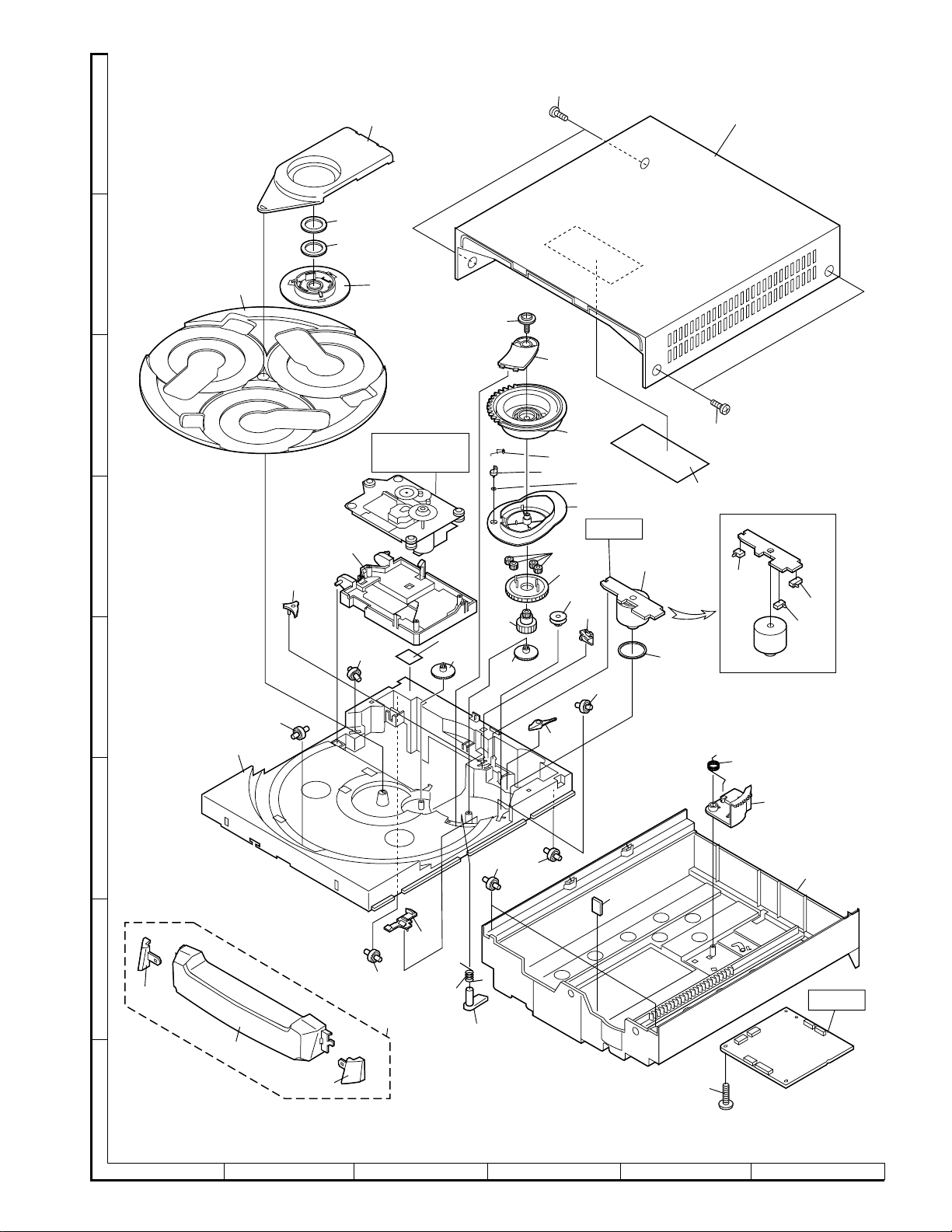
604x2
CD-DP2500W/DK2500W
A
279
205
258
257
B
283
265
612
266
C
CD
MECHANISM
284
263
278
260
604x2
252
269
PWB-F
D
268
281
261
253
270
271
272x4
273
274
277
M3
SW3
SW1
SW2
251
275
E
261
261
282
276
285
264
F
261x3
280
255
262
G
204-2
261
204
286
PWB-C
267
204-1
204-3
H
616
1
23456
Figure 12 CABINET EXPLODED VIEW (3/3)
– 12 –
Page 68

CD-DP2500W/DK2500W
FRONT SPEAKER
A
B
C
903
912x2
912x4
901
RED
RED
BK
917
(with
Capacitor C1,2)
TWEETER
SP3(L-CH)
SP4(R-CH)
SUPER
TWEETER
SP1(L-CH)
SP2(R-CH)
BK
RED
C1,2
Capacitor
BK
WOOFER
SP5(L-CH)
SP6(R-CH)
907
D
E
F
G
H
SP3,4
914x2
SUPER
TWEETER
SP1(L-CH)
SP2(R-CH)
TWEETER
SP3(L-CH)
SP4(R-CH)
WOOFER
SP5(L-CH)
SP6(R-CH)
909x2
910
913x4
SP1,2
914x2
SP5,6
C1,2
Capacitor
2.2 µF,100V,
Electrolytic (N.P.)
916
916
905
916
909x2
916
910
1
23456
Figure 13 SPEAKER EXPLODED VIEW (1/2)
– 13 –
Page 69

CD-DP2500W/DK2500W
CENTER SPEAKER
A
B
C
904x4
905
904x4
903
901
902
SP1
906x4
D
SURROUND SPEAKER
E
F
SP1,2
G
SP1,2
901
904x6
905
903
902
H
1
23456
Figure 14 SPEAKER EXPLODED VIEW (2/2)
– 14 –
Page 70

CD-DP2500W/DK2500W
– MEMO –
– 15 –
Page 71

– MEMO –
CD-DP2500W/DK2500W
– 16 –
Page 72

CD-DP2500W/DK2500W
COPYRIGHT © 2000 BY SHARP CORPORATION
ALL RIGHTS RESERVED.
No part of this publication may be reproduced,
stored in a retrieval system, or transmitted in
any form or by any means, electronic, mechanical,
photocopying, recording, or otherwise, without
prior written permission of the publisher.
SHARP CORPORATION
Communication Systems Group
Quality & Reliability Control Center
Higashihiroshima, Hiroshima 739-0192, Japan
Printed in Japan
A0004-714SS•HA•M
EX
 Loading...