

Page 1
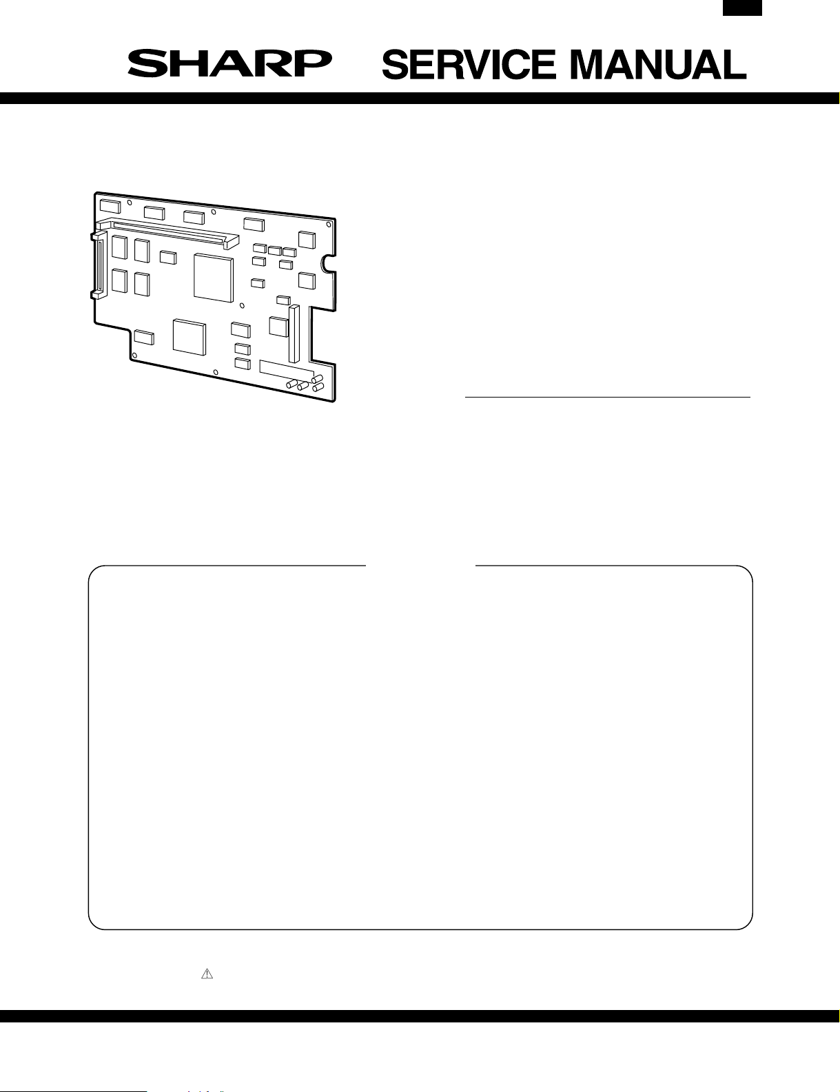
AR-PB9
CODE: 00ZARPB9//A1E
DIGITAL COPIER
OPTION PRINTER
EXPANSION KIT
MODEL AR-PB9
CONTENTS
[ 1 ] SYSTEM CONFIGURATION . . . . . . . . . . . . . . . . . 1 - 1
[ 2 ] SPECIFICATION . . . . . . . . . . . . . . . . . . . . . . . 1 - 1
[ 3 ] SET UP . . . . . . . . . . . . . . . . . . . . . . . . . . . . 3 - 1
[ 4 ] TROUBLE CODE LIST . . . . . . . . . . . . . . . . . . . . 4 - 1
[ 5 ] ELECTRICAL SECTION . . . . . . . . . . . . . . . . . . . 5 - 1
[ 6 ] CIRCUIT DIAGRAM . . . . . . . . . . . . . . . . . . . . . . 6 - 1
● PARTS GUIDE
Parts marked with “ ” are important for maintaining the safety of the set. Be sure to replace these parts with specified
ones for maintaining the safety and performance of the set.
This document has been published to be used
SHARP CORPORATION
for after sales service only.
The contents are subject to change without notice.
Page 2
AR-PB9
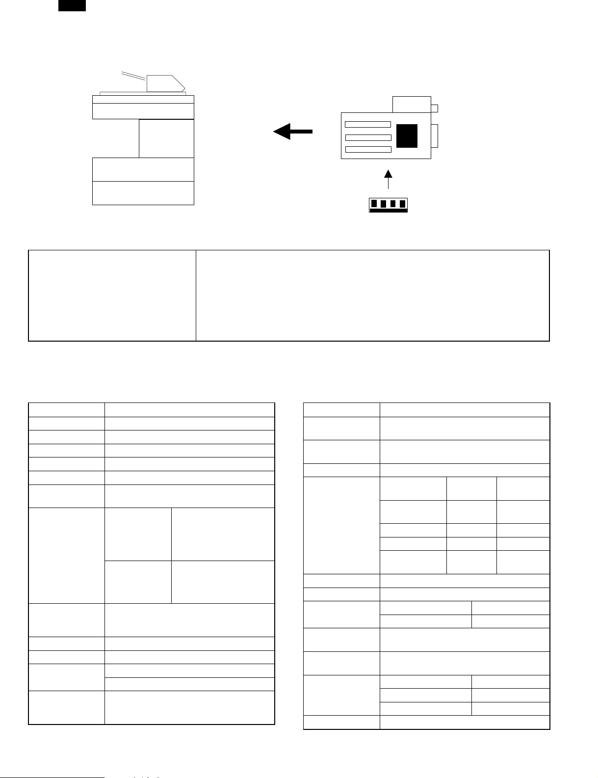
[1] SYSTEM CONFIGURATION
Printer expansion kit
(AR-PB9)
AR-150N/155N
●
●
●
Items supplied together(*)
*: USB and Parallel cables are not included.
●
●
●
●
●
[2] SPECIFICATIONS
1. Basic specifications
Item Contents
Print speed 15 PPM
First print 9.6 sec
Resolution 600 dpi, 300 dpi
Toner save No
Duplex print Yes (for duplex capable copier)
Paper feed tray
Paper size
Page description
language
(standard)
Dot emulation None
Page protection Yes
Interface
(Standard)
Applicable
Interface Cable
Multi bypass tray
Tray 1, Tray 2
A4R, B5R, A5R, 8.5" ×
Multi bypass
tray
Tray 1 ∼ 2
PCL6 (PCL XL) emulation
PCL5e emulation
IEEE1284 port × 1
USB port × 1
Parallel cable compliant IEEE1284 and less
than 2.0m (Shield and earth equipped)
USB cable less than 2.0 m
14", 8.5" × 11"R, 8.5" ×
5.5"R, 8.5" × 13", 8.5" ×
12.4"R, DL, C5, COM10,
Monarch
A4R, B5R, A5R, 8.5" ×
14"R, 8.5" × 11"R, 8.5"
× 5.5"R, 8.5" × 13"R,
8.5" × 12.4"R
Expansion memory
(Commercially available 168 pin EDO DIMM: 16MB/32MB/64MB)
Operation Manual
Instruction Manual
Printer drivers
Installer
Screen Fonts
Makedisk Software
Status Monitor Software
USB driver
Item Contents
Auto Interface
Switching
Auto Emulation
Switching
Plug and Play Yes
Printer Driver(*)
Resident Font 45 outline fonts compatible to PCL6
Screen Font 45 outline fonts compatible to PCL6
Memory
Expansion Slot
for Memory
Expansion
Memory
Operation Panel
Applicable PC IBM PC-AT Compatibles
*: Only Win 98 can be used for USB users.
No
Yes
MS
Windows3.1
MS Windows95 Yes Yes
MS Windows98 Yes Yes
MS Windows
NT4.0
Standard Maximum
8MB 72MB
One DIMM slots
64MB, 32MB, 16MB
(commercially-available DIMM:EDO)
Switches 1 (Online/Offline)
Lamps 2 (DATA, ONLINE)
Display None
PCL6
(PCL XL)
No Yes
Yes Yes
PCL5e
1 – 1
Page 3
Operations when both of USB/parallel ports are connected at the same time.
The USB port has a priority over the parallel port.
Smartsharing is invalid.
Interface connected previously Interface connected later Operation
USB (Unfinished print job YES/NO) Parallel port
Parallel port (Unfinished print job
YES/NO)
Parallel port (Unfinished print job
YES/NO)
USB
USB
USB: Enable
Parallel port: Disable
When USB is connected after 30sec of no communication through the
parallel port, the mode is shifted to the USB mode instantaneously.
If no communication state does not reach 30sec yet, shifting to the USB
mode is retained until 30sec passes. During that time, print jobs are
performed through the parallel port.
After completion of unfinished print jobs, if there is no communication for
30sec, shifting to the USB mode is made.
Within 30sec, print jobs are performed through the parallel port.
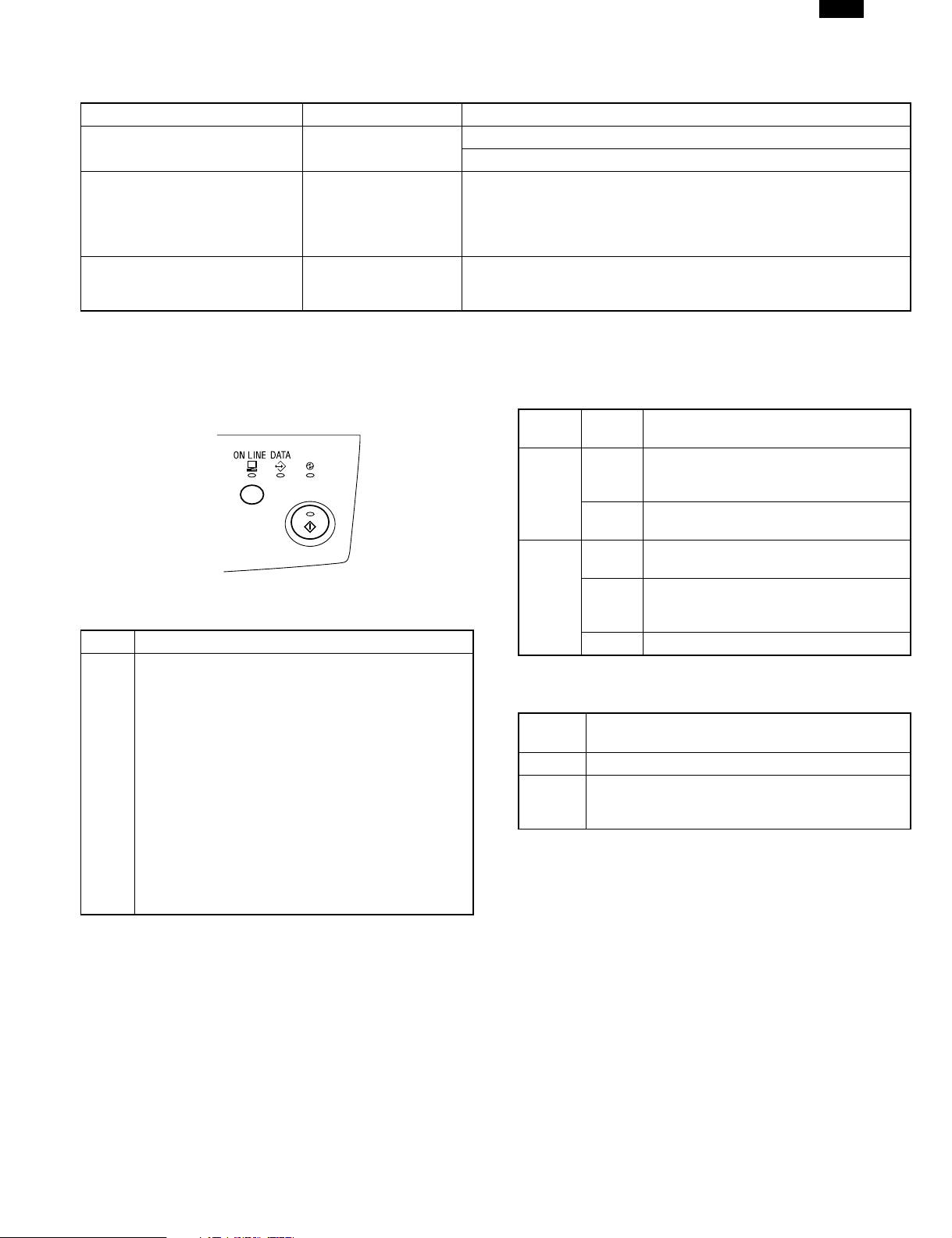
2. Control panel
The following are the components of the control panel.
AR-PB9
The table below lists the functions of the LEDs:
The table below lists the functions of the keys:
Key Functions
If pressed when the machine is in online status:
●
If no print job is being processed (DATA LED unlit),
pressing the LINE key produces the offline. If “Data
Loss Error” or “Memory Full” was displayed, pressing
the LINE key is disregarded.
●
If a 1-sided print job is being processed (Data LED lit or
LINE
flashing), pressing the LINE key produces the offline. If
“Data Loss Error” or “Memory Full” was displayed,
pressing the LINE key is disregarded.
●
If a 2-sided print job is being processed (Data LED lit or
flashing), pressing the LINE key has no effect.
If pressed when the machine is in the offline status:
●
Pressing the LINE key produces the online status and
causes the display mode to Online Display Mode.
LED
name
ONLINE
DATA
The table below shows the initial states of the LEDs just after the
power is turned ON.
LED
names
ONLINE Lit (online)
DATA
State Description
The printer unit is not ready to receive
Unlit
Lit
Unlit
Lit
Flash Printer data is remained without printing.
Initial state
Unlit
Will light immediately, however, if data has already
arrived when the power is turned ON.
data.
(Offline status)
The printer unit is ready to receive data.
(Online status)
No data is being received or processed.
(No print job is being processed)
The printer data is being received or
processed or Printed.
(A print job is being processed.)
1 – 2
Page 4
AR-PB9
[3] SET UP
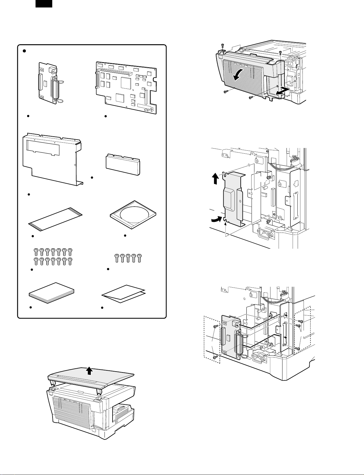
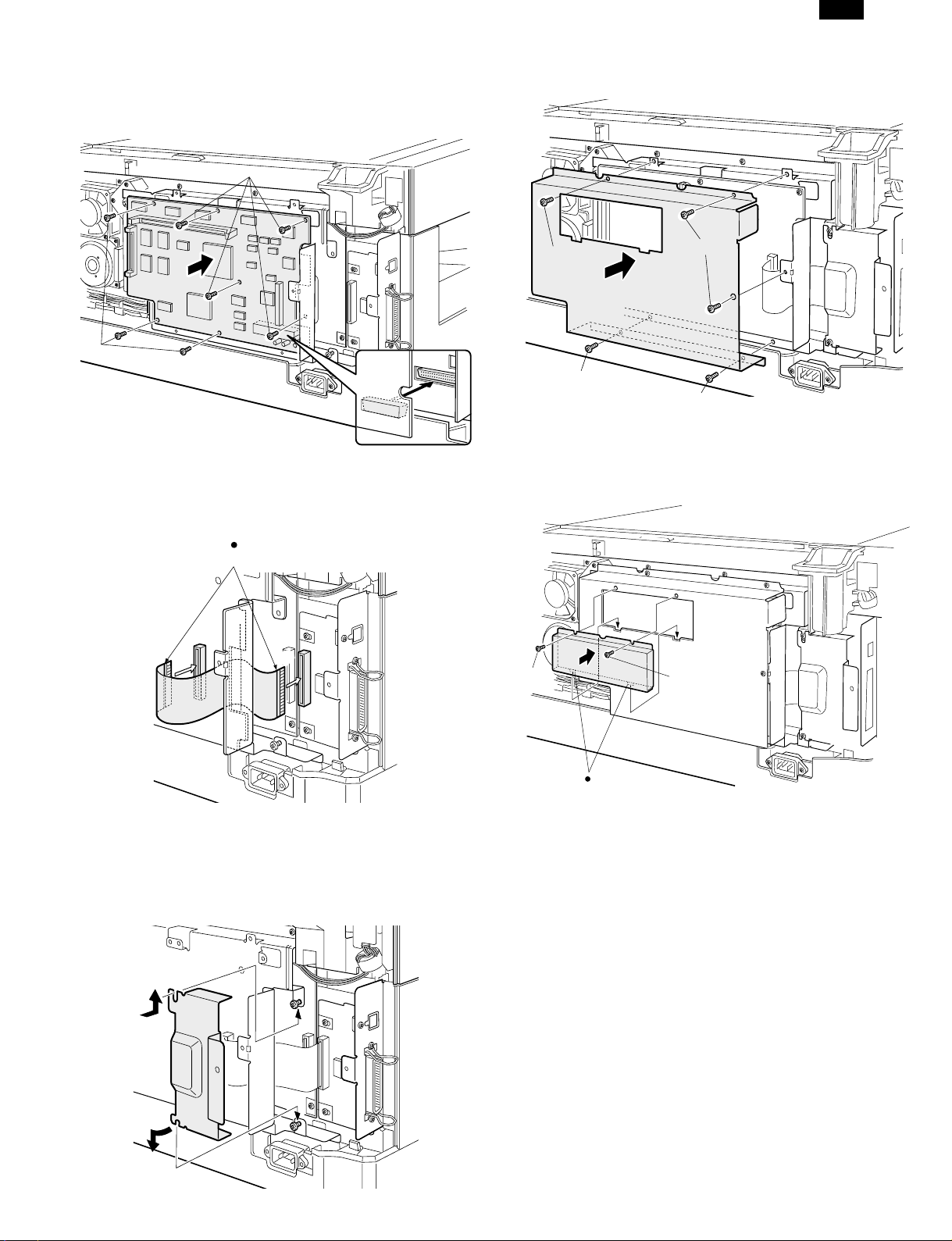
1. Installing Procedure
Parts included
PCL interface PWB, 1 pc.
PWB cover, 1 pc.
PCL PWB, 1 pc.
PWB cover lid 2, 1 pc.
2) Remove the rear cabinet.
● Remove the four screws and then remove the rear cabinet.
3) Remove the PWB cover.
(1) Loosen the screw that secures the PWB cover lid.
(2) Push up the PWB cover lid and
(3) Rotate it counterclockwise to remove it.
2
1
PCL harness, 1 pc.
Screws (M3 x 6), 14 pcs.
Operation Manual
Turn the main switch to the “OFF” position and remove the power plug
from the outlet.
1) Remove the document cover.
● Remove the document cover from the copier.
Screws (M3 x 8), 5 pcs.
Installation manual, 1 sheet
CD ROM
3
1
4) Attach the PCL interface PWB.
● Fit the connector of the PCL interface PWB into the mounting posi-
tion of the copier, secure the side A with three screws, and then
secure the front B with two screws.
A
B
M3X8
M3X8
3 – 1
Page 5
AR-PB9
5) Attach the PCL PWB.
● While ensuring that the connector of the PCL PWB is securely connected to that of the copier, attach the PCL PWB to the PWB cover
with seven screws (M3 × 6) and connect the relay harness connector.
M3X6
M3X6
6) Attach the PCL harness.
● Attach the supplied PCL harness to the PCL PWB, then pass it
through the square hole of the PWB holder, and connect it to the
PCL interface PWB.
Note: Be careful about the direction of the blue lines.
Blue lines
8) Attach the PWB cover.
● Attach the supplied PWB cover with five screws (M3 × 6).
M3X6
M3X6
M3X6
M3X6
9) Attach the PWB cover lid 2.
● Hang the pawls of the supplied PWB cover lid 2 on the PWB cover
and attach the PWB cover lid 2 with two screws (M3 × 6).
1
2
7) Attach the PWB cover.
(1) Fit the upper part of the PWB cover lid to the upper screw
that has been loosened in step 3 above.
(2) While rotating the lower part of the PWB cover lid clock-
wise, fit it to the lower screw.
(3) Tighten the upper and lower screws to secure the cover lid.
2
3
M3X6
M3X6
Pawls
1
3
3 – 2
Page 6
AR-PB9
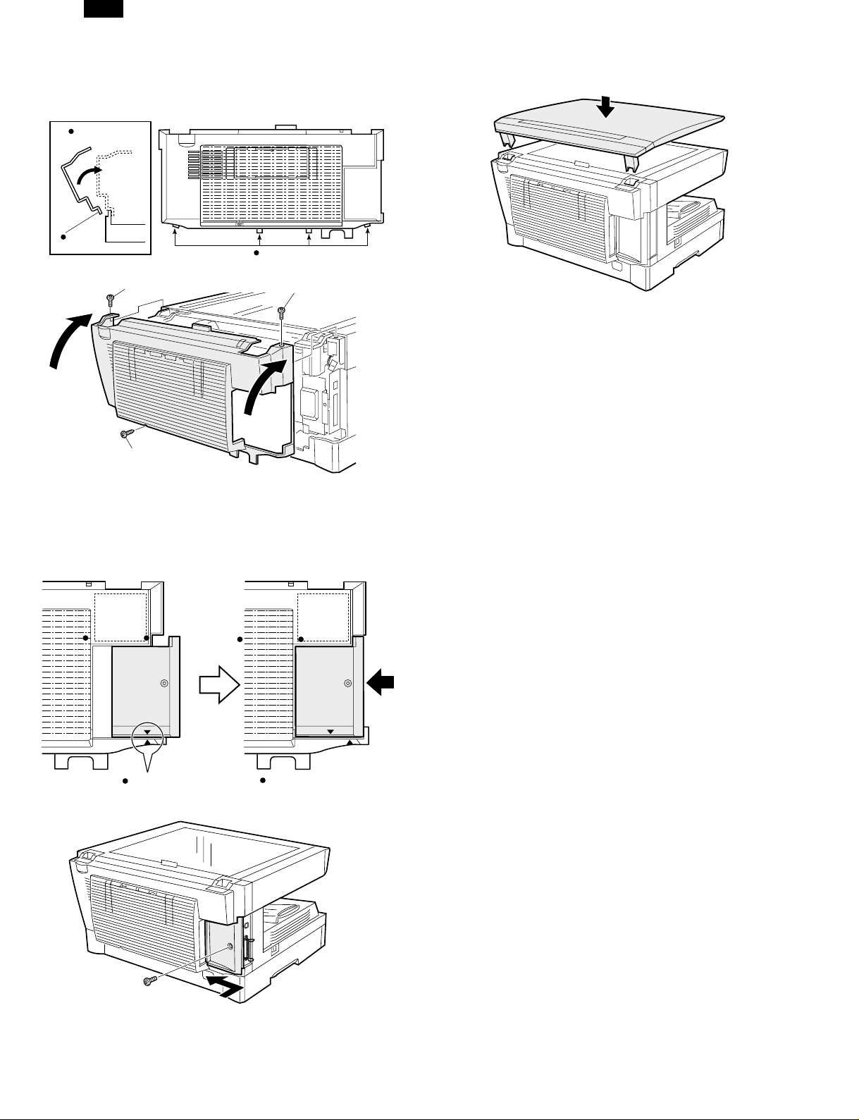
10) Attach the rear cabinet.
(1) Hang the four pawls shown in the illustration below on the
plate.
(2) Position the cabinet to the upper screw positions.
Side view
Pawl
Pawl
M3X8
M4X12
M3X8
12) Attach the document cover.
● Remove the document cover from the copier.
● Insert the power plug into the outlet and turn the main switch of the
copier to the “ON” position.
● Installation of the AR-PB9 is now complete.
2. INSTALLING THE PRINTER DRIVER
(Description of the printer driver)
The printer driver is the software program which runs the printer. It converts the data in your file into information that the printer can understand. It also controls communication between the printer and
computer as the data is printed.
11) Attach the cover to the rear cabinet.
(1) Align the arrow marks as shown in the illustration.
(2) Then slide the cover to the left.
(3) Secure the cover with a screw.
Arrow marks
After sliding
(Checking the hardware and software
requirements)
You will need the following hardware and software in order to install the
printer driver.
Computer type IBM PC/AT or compatible computer equipped
with a bi-directional parallel or USB interface,
and CD-ROM drive
Windows type Windows 3.1x, Windows 95, Windows 98*,
Windows NT 4.0 * USB is supported on Win-
dows 98 preinstalled only.
CPU 486DX 66MHz or better
Physical RAM Windows 95, Windows 3.1x: 8MB (16MB or
more is recommended.)
Windows NT 4.0: 12MB (16MB or more is
recommended.)
Windows 98: 16MB (32MB or more is recom-
mended.)
Display 640 × 480 dots (VGA) or better
Hard disk free space 10MB or more
Caution: The printer driver included in this product cannot be
used under Windows NT 3.5x, OS/2, pure MS-DOS
and other operating systems which are not described
above.
Note: The PCL6 printer driver is not available in Windows 3.1
environment.
(Installing the printer driver)
The software for your printer is provided on CD-ROM.
Before installing the printer driver, be sure to check the following items.
● Is the printer connected properly to the computer?
● Does the printer have paper?
A. Windows 95/Windows NT 4.0 Installation
Instructions:
With both the computer and the printer turned off, connect the printer
to the computer with a parallel interface cable.
1) Load paper into the paper tray of the printer. For instructions
on loading paper, see the section LOADING COPY PAPER in
the copier operation manual.
2) Turn on the printer.
3 – 3
Page 7
AR-PB9
3) Turn on your computer and start Windows.
Note: Before installing the printer driver, be sure to close all
other applications which may be open.
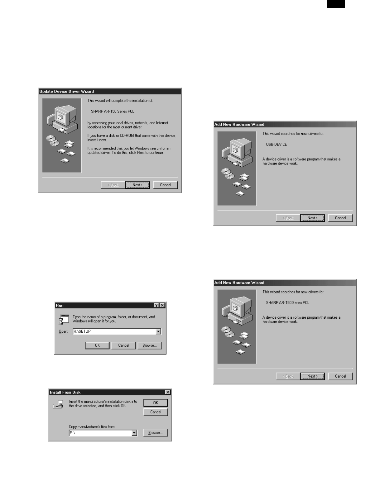
4) When using Windows 95 on a personal computer with plug &
play*, the “Update Device Driver Wizard” window will appear. Insert the installation CD-ROM into the CD-ROM drive. Click the
Next button and follow the on-screen instructions. If the “Copy-
ing Files” window appears during this operation, enter R:\ (if the
CD-ROM is designated as drive R), click the OK button and follow the on-screen instructions.
● If you use Windows 95 and the “New Hardware Found” window will
appear, select Driver from Disk Provided by Hardware Manufacturer
and then click the OK button. Proceed to step 6.
● If you use Windows 95 and the screen shown above or the “New
Hardware Found” window does not appear, proceed to step 5.
● If you use Windows NT 4.0, proceed to step 5.
* Plug & play
This feature is effective if both the computer and peripheral equipment
are equipped with IEEE 1284 compliant parallel interface.
Note: The screen displayed depends on the version of Win-
dows you are using.
5) Insert the installation CD-ROM into the CD-ROM drive.
Click the Start button and select Run. When the screen shown
below appears, type R:\SETUP (if the CD-ROM is designated
as drive R) and click the OK button. Follow the on-screen instructions.
B. Windows 98:
With both the computer and the printer turned off, connect the printer
to the computer with either a parallel or a USB interface cable.
1) Load paper into the paper tray of the printer. For instructions
on loading paper, see the section LOADING COPY PAPER
found in the copier operation manual.
2) Turn on the printer.
3) Turn on your computer and start Windows.
When using the USB interface:
● Connect your personal computer and the printer using a USB inter-
face cable if you have not already done so. (For information about
connecting the USB interface cable)
● When the “Add New Hardware Wizard” window appears, insert the
installation CD-ROM, click the Next button, follow the on-screen instructions, and finally click the Finish button.
Note: Before installing the printer driver, be sure to close all
other applications which may be open.
4) When using Windows 98 on a personal computer with plug &
play*, the “Add New Hardware Wizard” window will appear.
Click the Next button and follow the on-screen instructions.
● If the “Add New Hardware Wizard” window does not appear, proceed
to step 8.
6) The “Install From Disk” window will appear. Insert the installation CD-ROM into the CD-ROM drive. Type R:\ (if the CD-ROM
is designated as drive R) and click the OK button. Follow the
on-screen instructions.
Note: If you have any problem with the test print, check the
symptoms and solutions. Print the test page again after
resolving the problem.
5) Select Search for the best driver for your device and click the
Next button.
6) Insert the installation CD-ROM into the CD-ROM drive. (If you
are using the USB interface, confirm that the installation CDROM is in the CD-ROM drive.) Select the CD-ROM drive and
click the Next button.
3 – 4
Page 8
AR-PB9
7) Windows driver file search will find the device “SHARP AR-150
Series PCL”. Click the Next button and follow the on-screen instructions.
8) Insert the installation CD-ROM into the CD-ROM drive. (If you
are using the USB interface, confirm that the installation CDROM is in the CD-ROM drive.) Click the Start button and select
Run. When the window shown below appears, type R:\SETUP
(if the CD-ROM is designated as drive R) and click the OK button. Follow the on-screen instructions.
For proper uninstallation, be sure to use the SHARP uninstall program
of the printer driver group.
Readme
The latest information on the printer driver is included in this document.
Read the Readme first.
Status Monitor
The Status Monitor window provides visual information about the
printer state and current job.
Status Monitor HELP
Assistance and information for Status Monitor.
● Be sure to read the “Readme” document found in the printer driver
group before using your SHARP AR-150 Series PCL printer.
● You cannot use both the status monitor and the Print Manager at the
same time in Windows 3.1 environment.
3. TEST PRINTING
To test print the configuration page and font list, use the following procedure:
1) Press and hold down the light and dark keys simultaneously for
more than 5 seconds until all the alarm indicators blink and “--”
appears in the display.
2) Set “6” (configuration page) or “7” (font list) using the left copy
quantity key. The selected number will blink in the left side of
the display.
3) Press the print key. The entered program number will be steadi-
ly lit and the currently selected parameter number for the program will blink on the right side of the display.
4) Select the desired parameter using the right copy quantity key.
The entered parameter number will blink on the right of the display.
C. Windows 3.1x:
With both the computer and the printer turned off, connect the printer
to the computer with a parallel interface cable.
1) Load paper into the paper tray of the printer. For instructions
on loading paper, see the section LOADING COPY PAPER in
the copier operation manual.
2) Turn on the printer and then start Windows on your computer.
Note: Before installing the printer driver, be sure to close all
other applications which may be open.
3) Insert the installation CD-ROM into the CD-ROM drive.
4) Choose File from the Menu bar in Program Manager, and then
choose the Run... command.
5) Type R:\SETUP (if the CD-ROM is designated as drive R) in
the command line box and then click the OK button.
6) Follow the on-screen instructions.
D. AR-150 Series PCL printer driver group
When you install the printer driver, the SHARP AR-150 Series PCL
printer driver group is automatically created. The printer driver group includes the following items:
Uninstall AR-150 Series PCL
The printer driver can be uninstalled. If the driver is uninstalled, printing
can no longer be performed on the printer.
Program
No.
6
7 Font list
5) Press the print key. The test page prints.
Note: To change the setting or to set another mode, press the
Configuration Page items
1st level item 2nd level item 3rd level item
Hardware Status
Mode Parameters
Configu-
ration
page
clear key. The printer will return to step 2.
0 → English 1 → French 2 → Spanish
3 → Italian 4 → German
0 → English 1 → French 2 → Spanish
3 → Italian 4 → German
Machine Information Language
Hardware Specs
Processor 64 bit RISC
Interface Menu I/O Timeout
ROM Version
Total Page Count
Version Information PCL6
Input Paper Tray
Basic Memory
Total Memory
Bypass Tray
Tray 1
Tray 2
3 – 5
Page 9
[4] TROUBLE CODE LIST
Main
Sub
code
code
F9 10 Content Printer PWB trouble
Detail Communication trouble between
Cause Printer PWB connector
Check
and
remedy
80 Content Printer PWB communication trouble
Detail Communication trouble between
Cause Printer PWB connector
Check
and
remedy
81 Content Printer PWB communication trouble
Detail Communication trouble between
Cause Printer PWB connector
Check
and
remedy
82 Content Printer PWB communication trouble
Detail Communication trouble between
Cause Printer PWB connector
Check
and
remedy
MCU and PRT
disconnection
Printer unit PWB MCU PWB
harness failure
Printer PWB ROM defect, data
failure
Check the connectors and harness
of the printer PWB and the MCU
PWB.
Check grounding of the machine.
Check the ROM of the printer PWB.
(protocol)
MCU and printer PWB (Protocol
error)
disconnection
Printer PWB MCU PWB harness
failure
Printer PWB ROM defect, data
failure
Check the connectors and harness
of the printer PWB and the MCU
PWB.
Check grounding of the machine.
Check the ROM of the printer PWB.
(Parity)
MCU and printer PWB (Parity error)
disconnection
Printer PWB MCU PWB harness
failure
Printer PWB ROM defect, data
failure
Check the connectors and harness
of the printer PWB and the MCU
PWB.
Check grounding of the machine.
Check the ROM of the printer PWB.
(Overrun)
MCU and printer PWB (Overrun
error)
disconnection
Printer PWB MCU PWB harness
failure
Printer PWB ROM defect, data
failure
Check the connectors and harness
of the Printer PWB and the MCU
PWB.
Check grounding of the machine.
Check the ROM of the Printer
PWB.
Detail of trouble
AR-PB9
Main
code
Sub
code
F9 84 Content Printer PWB communication trouble
Detail Communication trouble between
Cause Printer PWB connector
Check
and
remedy
88 Content Printer PWB communication trouble
Detail Communication trouble between
Cause Printer PWB connector
Check
and
remedy
(Framing)
MCU and printer PWB (Framing
error)
disconnection
Printer PWB MCU PWB harness
failure
Printer PWB ROM defect, data
failure
Check the connectors and harness
of the Printer PWB and the MCU
PWB.
Check grounding of the machine.
Check the ROM of the Printer
PWB.
(Time-out)
MCU and printer PWB (Time-out
error)
disconnection
Printer PWB MCU PWB harness
failure
Printer PWB ROM defect, data
failure
Check the connectors and harness
of the Printer PWB and the MCU
PWB.
Check grounding of the machine.
Check the ROM of the Printer
PWB.
Detail of trouble
4 – 1
Page 10
AR-PB9
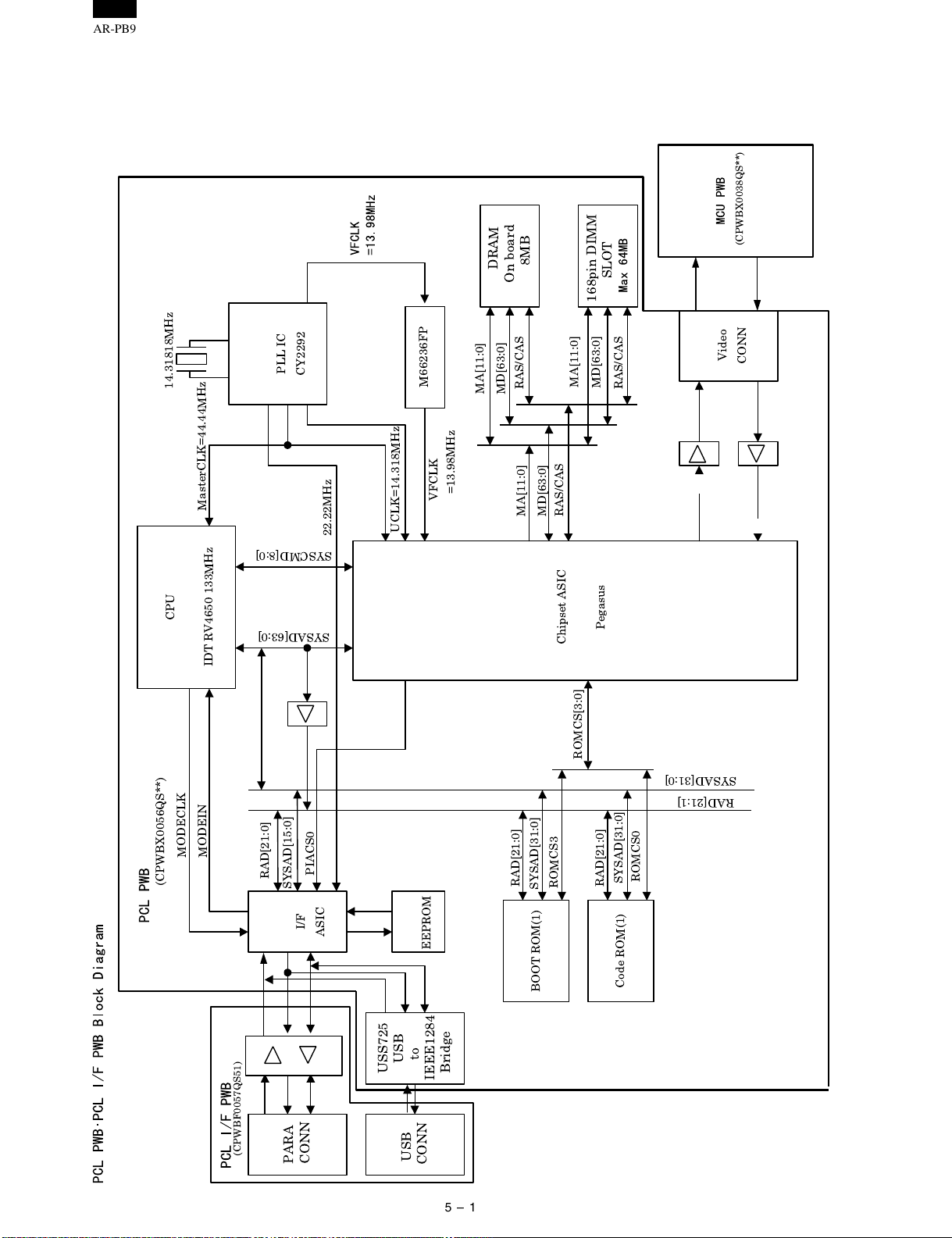
[5] ELECTRICAL SECTION
1. Block diagram
A. Overall block diagram
PLL IC
14.31818MHz
CY2292
M66236FP
DRAM
On board
MA[11:0]
MD[63:0]
8MB
RAS/CAS
SLOT
168pin DIMM
MA[11:0]
MD[63:0]
RAS/CAS
(CPWBX0038QS**)
Video
CONN
MasterCLK=44.44MHz
CPU
IDT RV4650 133MHz
MODECLK
MODEIN
(CPWBX0056QS**)
RAD[21:0]
SYSAD[15:0]
I/F
22.22MHz
SYSCMD[8:0]
SYSAD[63:0]
PIACS0
ASIC
=13.98MHz
VFCLK
UCLK=14.318MHz
EEPROM
MD[63:0]
MA[11:0]
RAD[21:0]
ROMCS3
SYSAD[31:0]
RAS/CAS
Chipset ASIC
ROMCS[3:0]
Pegasus
ROMCS0
SYSAD[31:0]
RAD[21:0]
SYSAD[31:0]
RAD[21:1]
(CPWBF0057QS51)
PARA
CONN
to
USB
USS725
USB
Bridge
IEEE1284
CONN
5 – 1
BOOT ROM(1)
Code ROM(1)
Page 11
AR-PB9
2. Block diagram functional descriptions
Descriptions of each block
PCL PWB Controls PCL print.
CPU Control IC
Chipset ASIC Image forming, ROM/RAM access
PLL IC
M66236FP Jitter adjustment IC
I/F ASIC
EEPROM
BOOTROM (1)
Code ROM (1)
USS725 USB to
IEEE1284 Bridge
DRAM On board 8MBWork RAM for the system and
168 pin DIMM
SLOT Max 64 MB
Video CONN
14.31818 MHz PLL IC reference clock
PCL I/F PWB Interface PWB for connection of
PARACONN
USB CONN USB connector
MCU PWB Digital copier main control PWB
CPU/ASIC/M66236fp clock
generation
IEEE1284 parallel conversion
ASIC
Stores device ID and data
necessary for control.
Stores data necessary for booting
programs.
Stores PCL process program and
fonts.
Converts USB standard signals
into IEEE1284 standard signals.
PCL process
Work RAM for PCL process
(Expanded by expansion RAM.)
Interface connector for
communication between MCU
PWB and PCL PWB
external device and PCL PWB
IEEE1284 conforming Centronics
connector
Operational descriptions
Connected to PARACONN or USBCONN of PCL I/F PWB
(CPWBF0057QS51).
Print data made by page description language is inputted from an external device.
The PCL I/F PWB (CPWBF0057QS51) is provided with two kinds of
connectors for external devices. The suitable connector is determined
according to the connection type with an external device as follows:
● An external device is connected to PARACONN, and not connected
to USBCONN.
→ Data sent from the external device connected to
PARACONN is printed.
● An external device is not connected to PARACONN, but connected
to USBCONN.
→ Data sent from the external device connected to USBCONN
is printed.
● An external device is connected to PARACONN, and connected to
USBCONN.
→ Data sent from the external device connected to USBCONN
is printed.
The external device connected to PARACONN is not recognized.
Data inputted to PCL I/F PWB is inputted to PCL PWB and PCLdecoded and converted to generate BITMAP data for print.
To generate BITMAP data for print, DRAM On board 8 MB and the expansion RAM inserted into the 168 pin DIMM are used as the work
area.
BITMAP data generated in PCL PWB are subject to jitter adjustment by
M66236FP, and inputted to MCU PWB through Video CONN to perform laser output and print.
5 – 2
Page 12

AR-PB9
CPU (VHIIDT79RC465) I/O pin arrangement list (PCL Model)
PIN
No.
Pin name Signal name IN/OUT Destination Function
1 N.C N.C N.C,
2 N.C N.C N.C
3 N.C N.C N.C
4 N.C N.C N.C
5 N.C N.C N.C
6 N.C N.C N.C
7 N.C N.C N.C
8 N.C N.C N.C
9 N.C N.C N.C
10 SYSAD11 SYSAD11 IN/OUT ASIC(KZ4H167V06), 16M FLASH,
System address data bus
8M FLASH, 74LVC16245
11 V
12 V
SS
CC
GND IN GND
3.3V IN Power source
13 SYSCMD8 SYSCMD8 OUT ASIC (KZ4H167V06) System command data bus
14 SYSAD42 SYSAD42 IN/OUT ASIC(KZ4H167V06), 74LVC16244 System address data bus
15 SYSAD10 SYSAD10 IN/OUT ASIC(KZ4H167V06), 16M FLASH,
System address data bus
8M FLASH, 74LVC16245
16 SYSCMD7 SYSCMD7 OUT ASIC (KZ4H167V06) System command data bus
17 V
18 V
SS
CC
GND IN GND
3.3V IN Power source
19 SYSAD41 SYSAD41 IN/OUT ASIC(KZ4H167V06), 74LVC16244 System address data bus
20 SYSAD9 SYSAD9 IN/OUT ASIC(KZ4H167V06), 16M FLASH,
System address data bus
8M FLASH, 74LVC16245
21 SYSCMD6 SYSCMD6 OUT ASIC (KZ4H167V06) System command data bus
22 SYSAD40 SYSAD40 IN/OUT ASIC(KZ4H167V06), 74LVC16244 System address data bus
23 V
24 V
SS
CC
25 SYSAD8 SYSAD8 IN/OUT ASIC(KZ4H167V06), 16M FLASH,
GND IN GND
3.3V IN Power source
System address data bus
8M FLASH, 74LVC16245
26 SYSCMD5 SYSCMD5 OUT ASIC (KZ4H167V06) System command data bus
27 SYSADC4 IN NC (3.3V pull up)
28 SYSADC0 IN NC (3.3V pull up)
29 V
30 V
SS
CC
GND IN GND
3.3V IN Power source
31 SYSCMD4 SYSCMD4 OUT ASIC (KZ4H167V06) System command data bus
32 SYSAD39 SYSAD39 IN/OUT ASIC(KZ4H167V06), 74LVC16244 System address data bus
33 SYSAD7 SYSAD7 IN/OUT ASIC(KZ4H167V06), 16M FLASH,
System address data bus
8M FLASH, 74LVC16245
34 SYSCMD3 SYSCMD3 OUT ASIC (KZ4H167V06) System command data bus
35 V
36 V
SS
CC
GND IN GND
3.3V IN Power source
37 SYSAD38 SYSAD38 IN/OUT ASIC(KZ4H167V06), 74LVC16244 System address data bus
38 SYSAD6 SYSAD6 IN/OUT ASIC(KZ4H167V06), 16M FLASH,
System address data bus
8M FLASH, 74LVC16245
39 MODECLOCK MODECLK OUT ASIC(KZ3H008302) Boot mode clock
40 WR RDY READY_ IN External IC write ready
41 SYSAD37 SYSAD37 IN/OUT ASIC(KZ4H167V06), 74LVC16244 System address data bus
42 SYSAD5 SYSAD5 IN/OUT ASIC(KZ4H167V06), 16M FLASH,
System address data bus
8M FLASH, 74LVC16245
5 – 3
Page 13

AR-PB9
PIN
No.
43 V
44 V
Pin name Signal name IN/OUT Destination Function
SS
CC
GND IN GND
3.3V IN Power source
45 N.C N.C N.C
46 N.C N.C N.C
47 N.C N.C N.C
48 N.C N.C N.C
49 N.C N.C N.C
50 N.C N.C N.C
51 N.C N.C N.C
52 N.C N.C N.C
53 N.C N.C N.C
54 N.C N.C N.C
55 N.C N.C N.C
56 N.C N.C N.C
57 SYSCMD2 SYSCMD2 OUT ASIC (KZ4H167V06) System command data bus
58 SYSAD36 SYSAD36 IN/OUT ASIC(KZ4H167V06), 74LVC16244 System address data bus
59 SYSAD4 SYSAD4 IN/OUT ASIC(KZ4H167V06), 16M FLASH,
System address data bus
8M FLASH, 74LVC16245
60 SYSCMD1 SYSCMD1 OUT ASIC (KZ4H167V06) System command data bus
61 V
62 V
SS
CC
GND IN GND
3.3V IN Power source
63 SYSAD35 SYSAD35 IN/OUT ASIC(KZ4H167V06), 74LVC16244 System address data bus
64 SYSAD3 SYSAD3 IN/OUT ASIC(KZ4H167V06), 16M FLASH,
System address data bus
8M FLASH, 74LVC16245
65 SYSCMD0 SYSCMD0 OUT ASIC (KZ4H167V06) System command data bus
66 SYSAD34 SYSAD34 IN/OUT ASIC(KZ4H167V06), 74LVC16244 System address data bus
67 V
68 V
SS
CC
69 SYSAD2 SYSAD2 IN/OUT ASIC(KZ4H167V06), 16M FLASH,
GND IN GND
3.3V IN Power source
System address data bus
8M FLASH, 74LVC16245
70 INT5 IN NC (3.3V pull up)
71 SYSAD33 SYSAD33 IN/OUT ASIC(KZ4H167V06), 74LVC16244 System address data bus
72 SYSAD1 SYSAD1 IN/OUT ASIC(KZ4H167V06), 16M FLASH,
System address data bus
8M FLASH, 74LVC16245
73 V
74 V
SS
CC
GND IN GND
3.3V IN Power source
75 INT4 IN NC (3.3V pull up)
76 SYSAD32 SYSAD32 IN/OUT ASIC(KZ4H167V06) System address data bus
77 SYSAD0 SYSAD0 IN/OUT ASIC(KZ4H167V06), 16M FLASH,
System address data bus
8M FLASH, 74LVC16245
78 INT3 PARINTR_ IN ASIC(KZ3H008302) Print request interruption input
79 V
80 V
SS
CC
GND IN GND
3.3V IN Power source
81 INT2 INTR2_ IN ASIC(KZ4H167V06) ASIC interruption 2
82 SYSAD16 SYSAD16 IN/OUT ASIC(KZ4H167V06), 16M FLASH,
System address data bus
8M FLASH
83 SYSAD48 SYSAD48 IN/OUT ASIC (KZ4H167V06), 16M FLASH,
System address data bus
8M FLASH, 74LVC16244
84 INT1 INTR1_ IN ASIC(KZ4H167V06) ASIC interruption 1
5 – 4
Page 14

AR-PB9
PIN
No.
85 V
86 V
87 SYSAD17 SYSAD17 IN/OUT ASIC(KZ4H167V06), 16M FLASH,
Pin name Signal name IN/OUT Destination Function
SS
CC
GND IN GND
3.3V IN Power source
System address data bus
8M FLASH
88 SYSAD49 SYSAD49 IN/OUT ASIC (KZ4H167V06), 74LVC244 System address data bus
89 INT0 INTR0_ IN ASIC(KZ4H167V06) ASIC interruption 0
90 SYSAD18 SYSAD18 IN/OUT ASIC(KZ4H167V06), 16M FLASH,
System address data bus
8M FLASH
91 V
92 V
SS
CC
GND IN GND
3.3V IN Power source
93 SYSAD50 SYSAD50 IN/OUT ASIC (KZ4H167V06), 74LVC244 System address data bus
94 VALID IN VALIN_ IN ASIC (KZ4H167V06) VALID INPUT (from ASIC)
95 SYSAD19 SYSAD19 IN/OUT ASIC(KZ4H167V06), 16M FLASH,
System address data bus
8M FLASH
96 SYSAD51 SYSAD51 IN/OUT ASIC (KZ4H167V06), 74LVC244 System address data bus
97 V
98 V
SS
CC
GND IN GND
3.3V IN Power source
99 VALID OUT VALOUT_ OUT ASIC (KZ4H167V06) VALID OUTPUT(to ASIC)
100 SYSAD20 SYSAD20 IN/OUT ASIC(KZ4H167V06), 16M FLASH,
System address data bus
8M FLASH
101 N.C N.C N.C
102 N.C N.C N.C
103 N.C N.C N.C
104 N.C N.C N.C
105 N.C N.C N.C
106 N.C N.C N.C
107 N.C N.C N.C
108 N.C N.C N.C
109 N.C N.C N.C
110 N.C N.C N.C
111 N.C N.C N.C
112 N.C N.C N.C
113 N.C N.C N.C
114 SYSAD52 SYSAD52 IN/OUT ASIC (KZ4H167V06), 74LVC244 System address data bus
115 EXT RQST EXTRQ_ IN ASIC(KZ4H167V06) External request
116 V
117 V
CC
SS
118 SYSAD21 SYSAD21 IN/OUT ASIC(KZ4H167V06), 16M FLASH,
3.3V IN Power source
GND IN GND
System address data bus
8M FLASH
119 SYSAD53 SYSAD53 IN/OUT ASIC (KZ4H167V06), 74LVC244 System address data bus
120 RDRDY READY_ IN ASIC(KZ4H167V06) External IC read ready
121 MODEIN MODEIN IN ASIC(KZ3H008302) Boot mode data input
122 SYSAD22 SYSAD22 IN/OUT ASIC(KZ4H167V06), 16M FLASH,
System address data bus
8M FLASH
123 SYSAD54 SYSAD54 IN/OUT ASIC (KZ4H167V06) System address data bus
124 V
125 V
CC
SS
3.3V IN Power source
GND IN GND
126 RELEASE RLS_ OUT ASIC(KZ4H167V06) Interface open state
5 – 5
Page 15

AR-PB9
PIN
No.
127 SYSAD23 SYSAD23 IN/OUT ASIC(KZ4H167V06), 16M FLASH,
Pin name Signal name IN/OUT Destination Function
System address data bus
8M FLASH
128 SYSAD55 SYSAD55 IN/OUT ASIC (KZ4H167V06) System address data bus
129 NMI NMI_ IN ASIC(KZ4H167V06) Non-maskable interruption
130 V
131 V
CC
SS
3.3V IN Power source
GND IN GND
132 SYSADC2 3.3V IN Power source
133 SYSADC6 3.3V IN Power source
134 SYSAD24 SYSAD24 IN/OUT ASIC(KZ4H167V06), 16M FLASH,
System address data bus
8M FLASH
135 V
136 V
CC
SS
3.3V IN Power source
GND IN GND
137 SYSAD56 SYSAD56 IN/OUT ASIC (KZ4H167V06) System address data bus
138 SYSAD25 SYSAD25 IN/OUT ASIC(KZ4H167V06), 16M FLASH,
System address data bus
8M FLASH
139 SYSAD57 SYSAD57 IN/OUT ASIC (KZ4H167V06) System address data bus
140 V
141 V
CC
SS
3.3V IN Power source
GND IN GND
142 N.C N.C N.C
143 SYSAD26 SYSAD26 IN/OUT ASIC(KZ4H167V06), 16M FLASH,
System address data bus
8M FLASH
144 SYSAD58 SYSAD58 IN/OUT ASIC (KZ4H167V06) System address data bus
145 N.C N.C N.C
146 V
147 V
CC
SS
148 SYSAD27 SYSAD27 IN/OUT ASIC(KZ4H167V06), 16M FLASH,
3.3V IN Power source
GND IN GND
System address data bus
8M FLASH
149 N.C N.C N.C
150 N.C N.C N.C
151 N.C N.C N.C
152 N.C N.C N.C
153 N.C N.C N.C
154 N.C N.C N.C
155 N.C N.C N.C
156 N.C N.C N.C
157 N.C N.C N.C
158 N.C N.C N.C
159 SYSAD59 SYSAD59 IN/OUT ASIC (KZ4H167V06) System address data bus
160 COLD RESET COLDRES_ IN ASIC(KZ4H167V06) Clod reset
161 SYSAD28 SYSAD28 IN/OUT ASIC(KZ4H167V06), 16M FLASH,
System address data bus
8M FLASH
162 V
163 V
CC
SS
3.3V IN Power source
GND IN GND
164 SYSAD60 SYSAD60 IN/OUT ASIC (KZ4H167V06) System address data bus
165 RESET CPURES_ IN ASIC(KZ4H167V06) CPU reset
166 SYSAD29 SYSAD29 IN/OUT ASIC(KZ4H167V06), 16M FLASH,
System address data bus
8M FLASH
167 SYSAD61 SYSAD61 IN/OUT ASIC (KZ4H167V06) System address data bus
5 – 6
Page 16

AR-PB9
PIN
No.
168 SYSAD30 SYSAD30 IN/OUT ASIC(KZ4H167V06), 16M FLASH,
Pin name Signal name IN/OUT Destination Function
System address data bus
8M FLASH
169 V
170 V
CC
SS
3.3V IN Power source
GND IN GND
171 SYSAD62 SYSAD62 IN/OUT ASIC (KZ4H167V06) System address data bus
172 SYSAD31 SYSAD31 IN/OUT ASIC(KZ4H167V06), 16M FLASH,
System address data bus
8M FLASH
173 SYSAD63 SYSAD63 IN/OUT ASIC (KZ4H167V06) System address data bus
174 V
175 V
176 V
CC
SS
OK VCCOK IN ASIC (KZ4H167V06),
CC
3.3V IN Power source
GND IN GND
VCC states effective
ASIC(KZ3H008302)
177 SYSADC3 IN NC (3.3V pull up)
178 SYSADC7 IN NC (3.3V pull up)
179 N.C N.C N.C
180 N.C N.C N.C
181 N.C N.C N.C
182 N.C N.C N.C
183 N.C N.C N.C
184 N.C N.C N.C
185 V
P 3.3V IN Power source
CC
186 VSSP GND IN GND
187 MASTER CLOCK MASTERCLK IN ASIC(KZ4H167V06), PLL
Master clock
IC(CY2292)
188 V
189 V
CC
SS
3.3V IN Power source
GND IN GND
190 SYSADC5 IN NC (3.3V pull up)
191 SYSADC1 IN NC (3.3V pull up)
192 V
193 V
CC
SS
GND IN GND
3.3V IN Power source
194 SYSAD47 SYSAD47 IN/OUT ASIC (KZ4H167V06), 74LVC16244 System address data bus
195 SYSAD15 SYSAD15 IN/OUT ASIC(KZ4H167V06), 16M FLASH,
System address data bus
8M FLASH, 74LVC16245
196 SYSAD46 SYSAD46 IN/OUT ASIC (KZ4H167V06), 74LVC16244 System address data bus
197 V
198 V
CC
SS
199 SYSAD14 SYSAD14 IN/OUT ASIC(KZ4H167V06), 16M FLASH,
3.3V IN Power source
GND IN GND
System address data bus
8M FLASH, 74LVC16245
200 SYSAD45 SYSAD45 IN/OUT ASIC (KZ4H167V06), 74LVC16244 System address data bus
201 SYSAD13 SYSAD13 IN/OUT ASIC(KZ4H167V06), 16M FLASH,
System address data bus
8M FLASH, 74LVC16245
202 SYSAD44 SYSAD44 IN/OUT ASIC (KZ4H167V06), 74LVC16244 System address data bus
203 V
204 V
SS
CC
205 SYSAD12 SYSAD12 IN/OUT ASIC(KZ4H167V06), 16M FLASH,
GND IN GND
3.3V IN Power source
System address data bus
8M FLASH, 74LVC16245
206 SYSCMDP IN NC (3.3V pull up)
207 SYSAD43 SYSAD43 IN/OUT ASIC(KZ4H167V06), 74LVC16244 System address data bus
208 N.C N.C N.C
5 – 7
Page 17

ChipsetASIC (VHIKZ4H167V06) I/O pin arrangement list (PCL Model)
AR-PB9
PIN
No.
1V
Pin name Signal name IN/OUT Destination Function
CC
3.3V IN Power source
2 SYSAD16 SYSAD16 IN/OUT CPU, 16M FLASH, 8M FLASH System address data bus
3 SYSAD17 SYSAD17 IN/OUT CPU, 16M FLASH, 8M FLASH System address data bus
4 SYSAD18 SYSAD18 IN/OUT CPU, 16M FLASH, 8M FLASH System address data bus
5 SYSAD19 SYSAD19 IN/OUT CPU, 16M FLASH, 8M FLASH System address data bus
6 SYSAD20 SYSAD20 IN/OUT CPU, 16M FLASH, 8M FLASH System address data bus
7 SYSAD21 SYSAD21 IN/OUT CPU, 16M FLASH, 8M FLASH System address data bus
8 SYSAD22 SYSAD22 IN/OUT CPU, 16M FLASH, 8M FLASH System address data bus
9V
CC
3.3V IN Power source
10 GND GND IN GND
11 SYSAD23 SYSAD23 IN/OUT CPU, 16M FLASH, 8M FLASH System address data bus
12 SYSAD24 SYSAD24 IN/OUT CPU, 16M FLASH, 8M FLASH System address data bus
13 SYSAD25 SYSAD25 IN/OUT CPU, 16M FLASH, 8M FLASH System address data bus
14 SYSAD26 SYSAD26 IN/OUT CPU, 16M FLASH, 8M FLASH System address data bus
15 SYSAD27 SYSAD27 IN/OUT CPU, 16M FLASH, 8M FLASH System address data bus
16 SYSAD28 SYSAD28 IN/OUT CPU, 16M FLASH, 8M FLASH System address data bus
17 SYSAD29 SYSAD29 IN/OUT CPU, 16M FLASH, 8M FLASH System address data bus
18 V
CC
3.3V IN Power source
19 GND GND IN GND
20 SYSAD30 SYSAD30 IN/OUT CPU, 16M FLASH, 8M FLASH System address data bus
21 SYSAD31 SYSAD31 IN/OUT CPU, 16M FLASH, 8M FLASH System address data bus
22 SYSAD32 SYSAD32 IN/OUT CPU System address data bus
23 SYSAD33 SYSAD33 IN/OUT CPU, 74LVC16244 System address data bus
24 SYSAD34 SYSAD34 IN/OUT CPU, 74LVC16244 System address data bus
25 SYSAD35 SYSAD35 IN/OUT CPU, 74LVC16244 System address data bus
26 SYSAD36 SYSAD36 IN/OUT CPU, 74LVC16244 System address data bus
27 V
CC
3.3V IN Power source
28 GND GND IN GND
29 SYSAD37 SYSAD37 IN/OUT CPU, 74LVC16244 System address data bus
30 SYSAD38 SYSAD38 IN/OUT CPU, 74LVC16244 System address data bus
31 SYSAD39 SYSAD39 IN/OUT CPU, 74LVC16244 System address data bus
32 SYSAD40 SYSAD40 IN/OUT CPU, 74LVC16244 System address data bus
33 SYSAD41 SYSAD41 IN/OUT CPU, 74LVC16244 System address data bus
34 SYSAD42 SYSAD42 IN/OUT CPU, 74LVC16244 System address data bus
35 SYSAD43 SYSAD43 IN/OUT CPU, 74LVC16244 System address data bus
36 GND GND IN GND
37 GND GND IN GND
38 GND GND IN GND
39 V
CC
3.3V IN Power source
40 SYSAD44 SYSAD44 IN/OUT CPU, 74LVC16244 System address data bus
41 SYSAD45 SYSAD45 IN/OUT CPU, 74LVC16244 System address data bus
42 SYSAD46 SYSAD46 IN/OUT CPU, 74LVC16244 System address data bus
43 SYSAD47 SYSAD47 IN/OUT CPU, 74LVC16244 System address data bus
44 SYSAD48 SYSAD48 IN/OUT CPU, 16M FLASH, 8M FLASH,
System address data bus
74LVC16244
45 SYSAD49 SYSAD49 IN/OUT CPU, 74LVC244 System address data bus
46 SYSAD50 SYSAD50 IN/OUT CPU, 74LVC244 System address data bus
5 – 8
Page 18

AR-PB9
PIN
No.
Pin name Signal name IN/OUT Destination Function
47 SYSAD51 SYSAD51 IN/OUT CPU, 74LVC244 System address data bus
48 V
CC
3.3V IN Power source
49 GND GND IN GND
50 SYSAD52 SYSAD52 IN/OUT CPU, 74LVC244 System address data bus
51 SYSAD53 SYSAD53 IN/OUT CPU, 74LVC244 System address data bus
52 SYSAD54 SYSAD54 IN/OUT CPU System address data bus
53 SYSAD55 SYSAD55 IN/OUT CPU System address data bus
54 SYSAD56 SYSAD56 IN/OUT CPU System address data bus
55 SYSAD57 SYSAD57 IN/OUT CPU System address data bus
56 SYSAD58 SYSAD58 IN/OUT CPU System address data bus
57 SYSAD59 SYSAD59 IN/OUT CPU System address data bus
58 V
CC
3.3V IN Power source
59 GND GND IN GND
60 SYSAD60 SYSAD60 IN/OUT CPU System address data bus
61 SYSAD61 SYSAD61 IN/OUT CPU System address data bus
62 SYSAD62 SYSAD62 IN/OUT CPU System address data bus
63 SYSAD63 SYSAD63 IN/OUT CPU System address data bus
64 V
CC
3.3V IN Power source
65 GND GND IN GND
66 MASTERCLK MASTERCLK IN PLL IC(CY2292) Master clock
67 TESTMODE IN Test pin (3.3V)
68 DC2_TEST IN Test pin (GND)
69 SCAN_TEST IN Test pin (GND)
70 SCAN_EN IN Scan enable (GND)
71 PLL_EN RESET_ IN 74LS244 PLL enable
72 PLL_TEST IN Test pin (GND)
73 GND GND IN GND
74 V
75 V
CC
CC
3.3V IN Power source
3.3V IN Power source
76 CPOUT OUT Charge pump output
77 PLLGND GND IN PLL GND
78 PLLVDD 3.3V IN PLL power
79 VCOIN IN Loop filter input
80 GND GND IN GND
81 SYSCMD8 SYSCMD8 IN/OUT CPU System command data bus
82 SYSCMD7 SYSCMD7 IN/OUT CPU System command data bus
83 SYSCMD6 SYSCMD6 IN/OUT CPU System command data bus
84 SYSCMD5 SYSCMD5 IN/OUT CPU System command data bus
85 SYSCMD4 SYSCMD4 IN/OUT CPU System command data bus
86 SYSCMD3 SYSCMD3 IN/OUT CPU System command data bus
87 SYSCMD2 SYSCMD2 IN/OUT CPU System command data bus
88 SYSCMD1 SYSCMD1 IN/OUT CPU System command data bus
89 V
CC
3.3V IN Power source
90 GND GND IN GND
91 SYSCMD0 SYSCMD0 IN/OUT CPU System command data bus
92 /DACK3 N.C NC
93 /DACK2 N.C NC
5 – 9
Page 19

AR-PB9
PIN
No.
Pin name Signal name IN/OUT Destination Function
94 /DACK1 N.C NC
95 /DACK0 PARACK_ OUT ASIC(KZ3H008302) ACK_ signal to interface ASIC
96 /CPURST CPURST_ OUT CPU CPU reset signal
97 /CRST COLDRES_ OUT CPU Cold reset signal
98 VCCOK VCCOK OUT CPU, ASIC(KZ3H008302) V
99 V
CC
3.3V IN Power source
states effective
CC
100 GND GND IN GND
101 /NMI NMI_ OUT CPU Non-maskable interruption output
102 /INTR2 INTR2_ OUT CPU Interruption output 2
103 /INTR1 INTR1_ OUT CPU Interruption output 1
104 /INTR0 INTR0_ OUT CPU Interruption output 0
105 /EXREQ EXREQ_ OUT CPU Bus open request
106 /READY READY_ OUT CPU Command reception ready from
CPU
107 /VALIN VALIN_ OUT CPU VALID INPUT(to CPU)
108 /PIARD PIARD_ OUT 74LVC16245, ASIC(KZ3H008302) External peripheral Read Enable
109 V
CC
3.3V IN Power source
110 GND GND IN GND
111 GND GND IN GND
112 GND GND IN GND
113 SCLK SCLK IN PLL IC(CY2292) Serial clock
114 /DREQ3 IN NC (3.3V pull up)
115 /DREQ2 IN NC (3.3V pull up)
116 /DREQ1 IN NC (3.3V pull up)
117 /DREQ0 PARREQ_ IN ASIC(KZ3H008302) DREQ_ signal from interface ASIC
118 /POR RESET_ IN 74LS244 Power on reset
119 /RLS RLS_ IN CPU Bus open recognition
120 /VALOUT VALOUT_ IN CPU VALID OUTPUT(from CPU)
121 /WAIT IN GND
122 /PIAWE PIAWE_ OUT ASIC(KZ3H008302) External peripheral Write Enable
123 /PIACS5 NC
124 /PIACS4 NC
125 /PIACS3 NC
126 /PIACS2 NC
127 V
CC
3.3V IN Power source
128 GND GND IN GND
129 /PIACS1 NC
130 /PIACS0 LDTOE_ , 1284CS_ OUT 74LVC16245, ASIC(KZ3H008302) Interface ASIC chip select
131 /ROMCS3 RCS3_ OUT NC
132 /ROMCS2 RCS2_ NC
133 /ROMCS1 RCS1_ OUT LH28F800SUT Boot ROM chip select
134 /ROMCS0 RCS0_ OUT LH28F016SUT Code ROM chip select
135 /MWE MWE_ OUT 74LVC16244 DRAM write enable
136 /MOE MOE_ OUT 74LVC16244 DRAM output enable
137 V
CC
3.3V IN Power source
138 GND GND IN GND
139 /CAS7 CAS7_ OUT 16M Flash, DIMM168 DRAM CAS_ signal
5 – 10
Page 20

AR-PB9
PIN
No.
Pin name Signal name IN/OUT Destination Function
140 /CAS6 CAS6_ OUT 16M Flash, DIMM168 DRAM CAS_ signal
141 /CAS5 CAS5_ OUT 16M Flash, DIMM168 DRAM CAS_ signal
142 /CAS4 CAS4_ OUT 16M Flash, DIMM168 DRAM CAS_ signal
143 /CAS3 CAS3_ OUT 16M Flash, DIMM168 DRAM CAS_ signal
144 /CAS2 CAS2_ OUT 16M Flash, DIMM168 DRAM CAS_ signal
145 /CAS1 CAS1_ OUT 16M Flash, DIMM168 DRAM CAS_ signal
146 /CAS0 CAS0_ OUT 16M Flash, DIMM168 DRAM CAS_ signal
147 GND GND IN GND
148 V
149 V
CC
CC
3.3V IN Power source
3.3V IN Power source
150 /RAS3 RAS3_ OUT NC
151 /RAS2 RAS2_ OUT 74LVC16244 DRAM RAS_ signal
152 /RAS1 RAS1_ OUT 74LVC16244 DRAM RAS_ signal
153 /RAS0 RAS0_ OUT 16M Flash DRAM RAS_ signal
154 MD63 MD63 IN/OUT 16M Flash, DIMM168 DRAM data signal
155 MD31 MD31 IN/OUT 16M Flash, DIMM168 DRAM data signal
156 MD62 MD62 IN/OUT 16M Flash, DIMM168 DRAM data signal
157 MD30 MD30 IN/OUT 16M Flash, DIMM168 DRAM data signal
158 V
CC
3.3V IN Power source
159 GND GND IN GND
160 MD61 MD61 IN/OUT 16M Flash, DIMM168 DRAM data signal
161 MD29 MD29 IN/OUT 16M Flash, DIMM168 DRAM data signal
162 MD60 MD60 IN/OUT 16M Flash, DIMM168 DRAM data signal
163 MD28 MD28 IN/OUT 16M Flash, DIMM168 DRAM data signal
164 MD59 MD59 IN/OUT 16M Flash, DIMM168 DRAM data signal
165 MD27 MD27 IN/OUT 16M Flash, DIMM168 DRAM data signal
166 MD58 MD58 IN/OUT 16M Flash, DIMM168 DRAM data signal
167 V
CC
3.3V IN Power source
168 GND GND IN GND
169 MD26 MD26 IN/OUT 16M Flash, DIMM168 DRAM data signal
170 MD57 MD57 IN/OUT 16M Flash, DIMM168 DRAM data signal
171 MD25 MD25 IN/OUT 16M Flash, DIMM168 DRAM data signal
172 MD56 MD56 IN/OUT 16M Flash, DIMM168 DRAM data signal
173 MD24 MD24 IN/OUT 16M Flash, DIMM168 DRAM data signal
174 MD55 MD55 IN/OUT 16M Flash, DIMM168 DRAM data signal
175 MD23 MD23 IN/OUT 16M Flash, DIMM168 DRAM data signal
176 V
CC
3.3V IN Power source
177 GND GND IN GND
178 MD54 MD54 IN/OUT 16M Flash, DIMM168 DRAM data signal
179 MD22 MD22 IN/OUT 16M Flash, DIMM168 DRAM data signal
180 MD53 MD53 IN/OUT 16M Flash, DIMM168 DRAM data signal
181 MD21 MD21 IN/OUT 16M Flash, DIMM168 DRAM data signal
182 MD52 MD52 IN/OUT 16M Flash, DIMM168 DRAM data signal
183 MD20 MD20 IN/OUT 16M Flash, DIMM168 DRAM data signal
184 GND GND IN GND
185 GND GND IN GND
186 GND GND IN GND
5 – 11
Page 21

AR-PB9
PIN
No.
187 V
Pin name Signal name IN/OUT Destination Function
CC
3.3V IN Power source
188 MD51 MD51 IN/OUT 16M Flash, DIMM168 DRAM data signal
189 MD19 MD19 IN/OUT 16M Flash, DIMM168 DRAM data signal
190 MD50 MD50 IN/OUT 16M Flash, DIMM168 DRAM data signal
191 MD18 MD18 IN/OUT 16M Flash, DIMM168 DRAM data signal
192 MD49 MD49 IN/OUT 16M Flash, DIMM168 DRAM data signal
193 MD17 MD17 IN/OUT 16M Flash, DIMM168 DRAM data signal
194 MD48 MD48 IN/OUT 16M Flash, DIMM168 DRAM data signal
195 V
CC
3.3V IN Power source
196 GND GND IN GND
197 MD16 MD16 IN/OUT 16M Flash, DIMM168 DRAM data signal
198 MD47 MD47 IN/OUT 16M Flash, DIMM168 DRAM data signal
199 MD15 MD15 IN/OUT 16M Flash, DIMM168 DRAM data signal
200 MD46 MD46 IN/OUT 16M Flash, DIMM168 DRAM data signal
201 MD14 MD14 IN/OUT 16M Flash, DIMM168 DRAM data signal
202 MD45 MD45 IN/OUT 16M Flash, DIMM168 DRAM data signal
203 MD13 MD13 IN/OUT 16M Flash, DIMM168 DRAM data signal
204 V
CC
3.3V IN Power source
205 GND GND IN GND
206 MD44 MD44 IN/OUT 16M Flash, DIMM168 DRAM data signal
207 MD12 MD12 IN/OUT 16M Flash, DIMM168 DRAM data signal
208 MD43 MD43 IN/OUT 16M Flash, DIMM168 DRAM data signal
209 MD11 MD11 IN/OUT 16M Flash, DIMM168 DRAM data signal
210 MD42 MD42 IN/OUT 16M Flash, DIMM168 DRAM data signal
211 MD10 MD10 IN/OUT 16M Flash, DIMM168 DRAM data signal
212 MD41 MD41 IN/OUT 16M Flash, DIMM168 DRAM data signal
213 V
CC
3.3V IN Power source
214 GND GND IN GND
215 MD9 MD9 IN/OUT 16M Flash, DIMM168 DRAM data signal
216 MD40 MD40 IN/OUT 16M Flash, DIMM168 DRAM data signal
217 MD8 MD8 IN/OUT 16M Flash, DIMM168 DRAM data signal
218 MD39 MD39 IN/OUT 16M Flash, DIMM168 DRAM data signal
219 MD7 MD7 IN/OUT 16M Flash, DIMM168 DRAM data signal
220 MD38 MD38 IN/OUT 16M Flash, DIMM168 DRAM data signal
221 MD6 MD6 IN/OUT 16M Flash, DIMM168 DRAM data signal
222 V
223 V
CC
CC
3.3V IN Power source
3.3V IN Power source
224 GND GND IN GND
225 MD37 MD37 IN/OUT 16M Flash, DIMM168 DRAM data signal
226 MD5 MD5 IN/OUT 16M Flash, DIMM168 DRAM data signal
227 MD36 MD36 IN/OUT 16M Flash, DIMM168 DRAM data signal
228 MD4 MD4 IN/OUT 16M Flash, DIMM168 DRAM data signal
229 MD35 MD35 IN/OUT 16M Flash, DIMM168 DRAM data signal
230 MD3 MD3 IN/OUT 16M Flash, DIMM168 DRAM data signal
231 MD34 MD34 IN/OUT 16M Flash, DIMM168 DRAM data signal
232 V
CC
3.3V IN Power source
233 GND GND IN GND
5 – 12
Page 22

AR-PB9
PIN
No.
Pin name Signal name IN/OUT Destination Function
234 MD2 MD2 IN/OUT 16M Flash, DIMM168 DRAM data signal
235 MD33 MD33 IN/OUT 16M Flash, DIMM168 DRAM data signal
236 MD1 MD1 IN/OUT 16M Flash, DIMM168 DRAM data signal
237 MD32 MD32 IN/OUT 16M Flash, DIMM168 DRAM data signal
238 MD0 MD0 IN/OUT 16M Flash, DIMM168 DRAM data signal
239 MA11 MA11 IN/OUT 74LVC16244 DRAM address signal
240 MA10 MA10 IN/OUT 74LVC16244 DRAM address signal
241 V
CC
3.3V IN Power source
242 GND GND IN GND
243 MA9 MA9 IN/OUT 74LVC16244 DRAM address signal
244 MA8 MA8 IN/OUT 74LVC16244 DRAM address signal
245 MA7 MA7 IN/OUT 74LVC16244 DRAM address signal
246 MA6 MA6 IN/OUT 74LVC16244 DRAM address signal
247 MA5 MA5 IN/OUT 74LVC16244 DRAM address signal
248 MA4 MA4 IN/OUT 74LVC16244 DRAM address signal
249 MA3 MA3 IN/OUT 74LVC16244 DRAM address signal
250 V
CC
3.3V IN Power source
251 GND GND IN GND
252 MA2 MA2 IN/OUT 74LVC16244 DRAM address signal
253 MA1 MA1 IN/OUT 74LVC16244 DRAM address signal
254 MA0 MA0 IN/OUT 74LVC16244 DRAM address signal
255 TXD1 CMD OUT 74LVC244 Serial data output 1
256 TXD2 N.C NC
257 /SYNCEN SYNCEN_ OUT M66236FP Jitter adjustment circuit control
signal
258 GND GND IN GND
259 GND GND IN GND
260 GND GND IN GND
261 V
CC
3.3V IN Power source
262 VFCLK VFCLK IN M66236FP Video I/F clock
263 RXD1 STS IN 74LS244 Serial data input 1
264 RXD2 IN NC (3.3V pull up)
265 /HSYNC HSYNC_ IN 74LS244 Print horizontal sync signal
266 /TC NC
267 /PAGE PAGE_ OUT 74LVC244 PAGE sync signal
268 /VDATA VDATA_ OUT 74LVC244 VIDEO data
269 /ROMWE ROMWE_ OUT 74LVC244 Flash ROM write enable
270 /BUFOE NC
271 /BUFDIR BUFDIR OUT 74LVC244 BUS buffer direction
272 V
CC
3.3V IN Power source
273 GND GND IN GND
274 SYSAD0 SYSAD0 IN/OUT CPU, 16M FLASH, 8M FLASH,
System address data bus
74LVC16245
275 SYSAD1 SYSAD1 IN/OUT CPU, 16M FLASH, 8M FLASH,
System address data bus
74LVC16245
276 SYSAD2 SYSAD2 IN/OUT CPU, 16M FLASH, 8M FLASH,
System address data bus
74LVC16245
5 – 13
Page 23

AR-PB9
PIN
No.
277 SYSAD3 SYSAD3 IN/OUT CPU, 16M FLASH, 8M FLASH,
Pin name Signal name IN/OUT Destination Function
System address data bus
74LVC16245
278 SYSAD4 SYSAD4 IN/OUT CPU, 16M FLASH, 8M FLASH,
System address data bus
74LVC16245
279 SYSAD5 SYSAD5 IN/OUT CPU, 16M FLASH, 8M FLASH,
System address data bus
74LVC16245
280 SYSAD6 SYSAD6 IN/OUT CPU, 16M FLASH, 8M FLASH,
System address data bus
74LVC16245
281 V
CC
3.3V IN Power source
282 GND GND IN GND
283 SYSAD7 SYSAD7 IN/OUT CPU, 16M FLASH, 8M FLASH,
System address data bus
74LVC16245
284 SYSAD8 SYSAD8 IN/OUT CPU, 16M FLASH, 8M FLASH,
System address data bus
74LVC16245
285 SYSAD9 SYSAD9 IN/OUT CPU, 16M FLASH, 8M FLASH,
System address data bus
74LVC16245
286 SYSAD10 SYSAD10 IN/OUT CPU, 16M FLASH, 8M FLASH,
System address data bus
74LVC16245
287 SYSAD11 SYSAD11 IN/OUT CPU, 16M FLASH, 8M FLASH,
System address data bus
74LVC16245
288 SYSAD12 SYSAD12 IN/OUT CPU, 16M FLASH, 8M FLASH,
System address data bus
74LVC16245
289 SYSAD13 SYSAD13 IN/OUT CPU, 16M FLASH, 8M FLASH,
System address data bus
74LVC16245
290 V
CC
3.3V IN Power source
291 GND GND IN GND
292 SYSAD14 SYSAD14 IN/OUT CPU, 16M FLASH, 8M FLASH,
System address data bus
74LVC16245
293 SYSAD15 SYSAD15 IN/OUT CPU, 16M FLASH, 8M FLASH,
System address data bus
74LVC16245
294 GND GND IN GND
295 GND GND IN GND
296 V
CC
3.3V IN Power source
5 – 14
Page 24

AR-PB9
Interface ASIC (VHIKZ3H008302) I/O pin arrangement list (PCL Model)
PIN
No.
1V
Pin name Signal name IN/OUT Destination Function
DD
3.3V IN Power source
2 CPUD13 LDT13 IN/OUT 74LVC16245 Data bus
3 CPUD14 LDT14 IN/OUT 74LVC16245 Data bus
4 CPUD15 LDT15 IN/OUT 74LVC16245 Data bus
5 MODECLK MODECLK OUT 74LS244 Boot mode clock
6 MODEIN MODEIN OUT CPU CPU boot mode setup serial data
output
7 CPUINTR_1 PARINTR_ OUT CPU Print request interruption output
8 DAMMY 1284-EN_ , USB-
EN_ , USB-ON
OUT USS-725, 74LVX244, I/F_CN IEEE1284/USB selection enable
signal
9 EREADY_1 PREADY_ OUT 74LVC244 Print ready signal
10 SRDY_1 SRDY_ OUT 74LVC244 PCL side reception ready signal
11 GND GND IN GND
12 GND GND IN GND
13 AD2 RAD2 IN/OUT 74LVC16244, 8M Flash, 16M Flash Address bus
14 AD3 RAD3 IN/OUT 74LVC16244, 8M Flash, 16M Flash Address bus
15 AD4 RAD4 IN/OUT 74LVC16244, 8M Flash, 16M Flash Address bus
16 AD5 RAD5 IN/OUT 74LVC16244, 8M Flash, 16M Flash Address bus
17 READY_1 EREADY_ IN 74LS244 MCU side ready signal
18 CRDY_1 CRDY_ IN 74LS244 MCU side reception ready signal
19 PSON_1 IN NC (3.3V pull up)
20 NETON_1 IN NC (3.3V pull up)
21 EXON_1 USB-IN IN I/F_CN USB input detection signal
22 SCK SCK IN 24C16 EEPROM serial clock
23 SDAOUT SDAOUT IN 24C16 EEPROM serial data output
24 SDAIN SDAIN IN 24C16 EEPROM serial data input
25 BSEL4 IN Process speed setup JP (3.3V pull
up)
26 BSEL3 IN Process speed setup JP (GND pull
down)
27 BSEL2 IN Process speed setup JP (GND pull
down)
28 BSEL1 IN Process speed setup JP (GND pull
down)
29 BSEL0 IN Process speed setup JP (3.3V pull
up)
30 SLCT SLCT OUT 74LCX244, USS-725 Printer selection state
31 FAULT_1 FAULT_ OUT 74LCX244, USS-725 Printer error
32 PE PE OUT 74LCX244, USS-725 Paper end
33 BUSY BUSY OUT 74LCX244, USS-725 Printer busy state
34 ACK_1 ACK_ OUT 74LCX244, USS-725 ACK status
35 STB_1 STB_ IN 74LCX244 STROBE control signal
36 AUTOFD_1 AUTOFD_ IN 74LCX244 Automatic new-line control signal
37 SLCTIN_1 SLCTIN_ IN 74LCX244 Printer selection
38 INIT_1 INIT_ IN 74LCX244 Printer initializing
39 PARAD7 PARAD7 IN 74LCX245, USS-725 Parallel I/F data bus
40 V
41 V
DD
DD
3.3V IN Power source
3.3V IN Power source
42 PARAD6 PARAD6 IN 74LCX245, USS-725 Parallel I/F data bus
5 – 15
Page 25

AR-PB9
PIN
No.
Pin name Signal name IN/OUT Destination Function
43 PARAD5 PARAD5 IN 74LCX245, USS-725 Parallel I/F data bus
44 GND GND IN GND
45 PARAD4 PARAD4 IN 74LCX245, USS-725 Parallel I/F data bus
46 PARAD3 PARAD3 IN 74LCX245, USS-725 Parallel I/F data bus
47 PARAD2 PARAD2 IN 74LCX245, USS-725 Parallel I/F data bus
48 V
DD
3.3V IN Power source
49 PARAD1 PARAD1 IN 74LCX245, USS-725 Parallel I/F data bus
50 PARAD0 PARAD0 IN 74LCX245, USS-725 Parallel I/F data bus
51 GND GND IN GND
52 GND GND IN GND
53 REV_1 REV_ OUT 74LCX245, I/F_CN Data direction control
54 SCAN_EN GND IN GND
55 SCAN_TEST GND IN GND
56 PDACK_1 PARACK_ IN ASIC(KZ4H167V06) DMA acknowledge signal from
ChipsetASIC
57 PDREQ_1 PARREQ_ OUT ASIC(KZ4H167V06) DMA request signal to ChipsetASIC
58 SCLK GA2CLK IN PLL IC (CY2292) Clock
59 DEVCS_1 1284CS_ IN ASIC(KZ4H167V06) OS_ signal to interface ASIC
60 DEVWR_1 PIAWE_ IN ASIC(KZ4H167V06) Write signal to interface ASIC
61 DEVRD_1 PIARD_ IN ASIC(KZ4H167V06), 74LVC16245 Read signal to interface ASIC
62 RES_1 RESET_ IN CPU Reset signal
63 VCCOK VCCOK IN ASIC(KZ4H167V06) VCC states effective
64 CPUD0 LDT0 IN/OUT 74LVC16245 Data bus
65 CPUD1 LDT1 IN/OUT 74LVC16245 Data bus
66 CPUD2 LDT2 IN/OUT 74LVC16245 Data bus
67 CPUD3 LDT3 IN/OUT 74LVC16245 Data bus
68 CPUD4 LDT4 IN/OUT 74LVC16245 Data bus
69 GND GND IN GND
70 CPUD5 LDT5 IN/OUT 74LVC16245 Data bus
71 CPUD6 LDT6 IN/OUT 74LVC16245 Data bus
72 V
DD
3.3V IN Power source
73 CPUD7 LDT7 IN/OUT 74LVC16245 Data bus
74 CPUD8 LDT8 IN/OUT 74LVC16245 Data bus
75 CPUD9 LDT9 IN/OUT 74LVC16245 Data bus
76 GND GND IN GND
77 CPUD10 LDT10 IN/OUT 74LVC16245 Data bus
78 CPUD11 LDT11 IN/OUT 74LVC16245 Data bus
79 CPUD12 LDT12 IN/OUT 74LVC16245 Data bus
80 V
DD
3.3V IN Power source
5 – 16
Page 26

AR-PB9
[6] CIRCUIT DIAGRAM
11
E
D
4.7K
4.7K
4.7K
4.7K
BR558-2
BR520-2
BR558-1
BR541-4
SYSAD30
SYSAD27
SYSAD28
SYSAD29
SYSAD27
SYSAD30
SYSAD28
SYSAD29
10
10
BR542-410BR540-2
BR542-2
4.7K
4.7K
BR516-3
BR541-2
SYSAD32
SYSAD31
SYSAD32
SYSAD31
-7-5-3-5-1-6-2-7-4
33
4.7K
4.7K
BR518-1
BR524-2
SYSAD34
SYSAD33
SYSAD34
SYSAD33
-5-7-7-7-5
4.7K
4.7K
4.7K
4.7K
BR538-2
BR519-1
BR528-3
BR518-4
SYSAD37
SYSAD38
SYSAD36
SYSAD35
SYSAD37
SYSAD36
SYSAD38
SYSAD35
10
10
BR509-710BR523-410BR523-2
BR510-810BR510-510BR511-610BR513-7
-5.-8-8-5-6-8-5-8-6-5-7-6-8
4.7K
4.7K
4.7K
4.7K
4.7K
4.7K
4.7K
BR530-4
BR543-2
BR543-4
BR543-3
BR543-1
BR530-2
BR519-4
SYSAD42
SYSAD41
SYSAD40
SYSAD43
SYSAD44
SYSAD45
SYSAD39
SYSAD41
SYSAD43
SYSAD40
SYSAD42
SYSAD44
SYSAD45
SYSAD39
-6-7-8-6-7-2-7-5-5
10
10
10
10
BR535-210BR537-4
BR535-4
BR529-310BR533-110BR531-210BR533-410BR537-2
BR525-3
-6-6-7-8-5-7-6-7-8
4.7K
4.7K
4.7K
4.7K
4.7K
4.7K
4.7K
4.7K
4.7K
BR517-1
BR516-1
BR517-3
BR526-1
BR520-3
BR526-3
BR555-4
BR521-4
BR521-2
SYSAD54
SYSAD53
SYSAD49
SYSAD48
SYSAD52
SYSAD51
SYSAD50
SYSAD46
SYSAD47
SYSAD54
SYSAD49
SYSAD50
SYSAD52
SYSAD48
SYSAD51
SYSAD53
SYSAD47
SYSAD46
-2-7-2-4-6-5-4-5-4
10
10
10
10
10
10
BR514-510BR546-110BR546-3
BR551-310BR542-3
BR549-3
BR515-510BR549-1
BR514-710BR515-710BR544-110BR542-1
BR513-5
44
(4-2C,2-4C,4-4A,5-4A)
E
D
SYSAD[63:0]
3.3V
-5-8-6-6-7-6-8-7-6
4.7K
4.7K
BR524-1
BR516-4
SYSAD2
SYSAD1
SYSAD0
SYSAD2
SYSAD1
SYSAD0
4.7K
4.7K
BR518-3
BR524-3
SYSAD3
SYSAD3
4.7K
4.7K
BR538-1
BR528-2
SYSAD5
SYSAD4
SYSAD5
SYSAD4
-3-4-6-1-7-1-8-1-7
4.7K
4.7K
BR538-3
BR519-2
SYSAD6
SYSAD7
SYSAD6
SYSAD7
-5-8-7-7-5-7-8-6-6
4.7K
4.7K
4.7K
BR536-1
BR530-3
BR538-4
SYSAD10
SYSAD9
SYSAD8
SYSAD10
SYSAD9
SYSAD8
4.7K
4.7K
BR536-3
BR536-2
SYSAD12
SYSAD11
SYSAD12
SYSAD11
10
10
BR535-110BR537-110BR535-3
BR533-310BR531-410BR531-110BR529-210BR525-210BR523-310BR523-110BR509-610BR510-710BR511-710BR511-510BR513-8
MODEL
QS
4.7K
4.7K
BR521-1
BR536-4
SYSAD13
SYSAD14
SYSAD13
SYSAD14
-6-5-6-8-1-8-8-6-3
4.7K
4.7K
BR516-2
BR521-3
SYSAD16
SYSAD15
SYSAD16
SYSAD15
SC,SIMPLEX
51
-5-7-7-5-6-7-5-8-5
4.7K
4.7K
4.7K
BR526-4
BR517-2
BR517-4
SYSAD18
SYSAD19
SYSAD17
SYSAD18
SYSAD19
SYSAD17
10
BR515-810BR514-610BR514-810BR513-610BR537-3
SC,DUPLEX
52
4.7K
4.7K
4.7K
BR557-3
BR520-4
BR526-2
SYSAD21
SYSAD22
SYSAD20
SYSAD21
SYSAD20
SYSAD22
-5-1-5-5-5-3-7-3-7
10
BR515-610BR549-410BR551-4
4.7K
BR557-2
SYSAD23
SYSAD23
10
BR549-2
-6-6-7-8-7-6-8-7-5
4.7K
4.7K
4.7K
BR557-1
BR558-3
BR558-4
SYSAD26
SYSAD25
SYSAD24
SYSAD25
SYSAD24
SYSAD26
10
BR546-410BR544-410BR546-210BR544-210BR540-4
4.7K
4.7K
BR555-3
BR555-2
SYSAD56
SYSAD55
SYSAD55
SYSAD56
4.7K
4.7K
BR554-4
BR555-1
SYSAD58
SYSAD57
SYSAD57
SYSAD58
-6-8-6-8-6-6-8-6-8
10
BR544-3
4.7K
4.7K
BR554-2
BR554-3
SYSAD60
SYSAD59
SYSAD59
SYSAD60
22
-6
4.7K
4.7K
BR541-3
BR554-1
SYSAD62
SYSAD61
SYSAD62
SYSAD61
10
BR540-3
4.7K
BR541-1
SYSAD63
SYSAD63
-8
10
BR540-1
180,181,182,183,184,
142,145,149,150,151,152,153,154,155,156,157,158,179,
101,102,103,104,105,106,107,108,109,110,111,112,113,
NC:1,2,3,4,5,6,7,8,9,45,46,47,48,49,50,51,52,53,54,55,56,
38
42
59
64
69
72
77
C
B
A
SYSAD1
SYSAD0
SYSADC1
SYSADC0
IC505
28
132
191
SYSADC2
SYSADC1
SYSADC0
-1
4.7KBR548-7
4.7KBR539-8
4.7KR953
3.3V
BR518-7
3.3V
BR528-8
BR528-5
BR530-1
BR519-6
BR522-8
BR522-7
BR522-6
BR522-5
SYSAD3
SYSAD2
SYSADC3
SYSADC2
27
177
SYSADC4
SYSADC3
4.7KR954
4.7KBR539-5
4.7K
4.7K
4.7K
4.7K
4.7K
4.7K
4.7K
4.7K
4.7K
SYSAD5
SYSAD4
SYSADC5
SYSADC4
190
SYSADC5
4.7K
BR539-7
-2
-1
-4
-8
-3
-1
-2
-3
-4
SYSAD7
SYSAD6
SYSADC7
SYSADC6
178
133
SYSADC7
SYSADC6
-3-1-2-4-2
4.7KBR539-6
BR548-8 4.7K
SYSAD9
SYSAD8
SYSCMD0
65
10BR510-3
SYSCMD0
SYSAD11
SYSAD10
SYSCMD2
SYSCMD1
57
60
10BR509-1
10BR509-4
SYSCMD1
SYSCMD2
SYSAD13
SYSAD12
SYSCMD4
SYSCMD3
31
34
10BR525-5
10BR525-8
SYSCMD4
SYSCMD3
SYSAD15
SYSAD14
SYSCMD6
SYSCMD5
21
26
10BR529-5
10BR529-8
SYSCMD6
SYSCMD5
SYSAD1782SYSAD16
SYSCMD8
SYSCMD7
13
16
-2-3-4-1-4-1-8-5-6
10BR533-7
10BR531-6
SYSCMD8
SYSCMD7
SYSAD1990SYSAD18
SYSCMDP
206
4.7K
R952
3.3V
3.3V
SYSAD21
SYSAD20
EXTRQST_
126
115
EXREQ_
(2-4A)
SYSAD24
SYSAD23
SYSAD22
RDRDY_
RELEASE_
WRRDY_
40
120
READY_
RLS_
(2-4A)
(2-4A)
SYSAD25
VALIDIN_
94
VALIN_
SYSAD28
SYSAD27
SYSAD26
MASTERCLK
VALIDOUT_
99
187
VALOUT_
(2-4A)
(2-4A)
4.7KBR556-8
4.7KBR556-6
4.7KBR556-7
4.7KR797
4.7KR798
4.7KBR548-6
SYSAD31
SYSAD30
SYSAD29
INT1_
INT0_
84
89
MASTERCLK
(2-1B,2-1C,2-3C)
-1
-3
-2
-3
81
INT2_
SYSAD3376SYSAD32
INT3_
78
INT4_
75
SYSAD3566SYSAD34
INT5_
70
4.7KBR524-5
3.3V
SYSAD3758SYSAD36
NMI_
129
SYSAD39
SYSAD38
VCCOK
176
SYSAD4122SYSAD40
RESET_
COLDRES_
39
165
160
SYSAD44
SYSAD4314SYSAD42
MODEIN
MODECLK
121
SYSAD46
SYSAD45
SYSAD47
3.3V
3.3V
SYSAD4983SYSAD48
SYSAD5193SYSAD50
185
SYSAD53
SYSAD52
VCCP
C579
SYSAD54
C569
C561
+
C514
C553
C556
C501
C507
+
C555
+
SYSAD56
SYSAD55
0.1u
0.1u
SYSAD58
SYSAD57
VSSP
186
22u
0.1u
0.1u
0.1u
0.1u
22u
22u
SYSAD59
SYSAD61
SYSAD60
SYSAD63
SYSAD62
17
11
GND
GND
VCC
VCC
VCC
24
18
12
85
79
73
67
61
35
23
GND
GND
GND
GND
GND
GND29GND
GND
VCC
VCC
VCC
VCC
VCC
VCC
VCC
VCC
86
80
74
68
62
36
30
116
0.1u
C682
0.1u
C683
0.1u
C684
0.1u
C685
0.1u
C686
C687
0.1u
0.1u
C688
0.1u
C689
0.1u
C690
189
175
170
163
136
131
125
117
GND
GND
GND
GND
GND
GND
GND
GND
VCC
VCC
VCC
VCC
VCC
VCC
VCC
VCC
188
174
169
162
140
135
130
124
C515
C516
C517
C518
C525
C526
C531
C533
C534
C535
203
198
193
147
141
97
43
GND
GND
GND
GND
GND
GND91GND
GND
VCC92VCC
VCC
VCC
VCC
VCC
VCC
98
44
204
197
146
192
C709
+
C708
+
0.1u
0.1u
0.1u
0.1u
0.1u
0.1u
0.1u
0.1u
0.1u
0.1u
C537
0.1u
0.1u
C538
C544
0.1u
0.1u
C548
0.1u
C550
0.1u
C554
0.1u
C559
0.1u
C560
0.1u
C562
0.1u
C563
IDT79RV4650-133DT
22u
22u
C
B
A
173
171
167
164
159
144
139
137
128
123
119
114
96
88
194
196
200
202
207
19
32
37
41
63
71
172
168
166
161
148
143
138
134
127
122
118
100
95
87
195
199
201
205
10
15
20
25
33
CPU
SYSCMD[8:0]
(2-4A)
INTR0_
(2-4A)
(2-4A)
INTR1_
INTR2_
PARINTR_
(2-4A)
(3-4A)
NMI_
(2-4A)
VCCOK
CPURES_
COLDRES_
(2-3A)
(2-3A)
(2-3A,3-3A)
MODEIN
MODECLK
(3-2A)
(3-3A)
6 – 1
Page 27

AR-PB9
3.3V
L507
SBO-02SAN
MD[63:0]SYSAD[63:0]
E
D
(6-4E)
MD0
238
IC512-2
254
MA0
MA[11:0]
(4-4C)
MD1
MD2
MD3
MD4
MD5
MD7
MD6
MD8
MD9
MD11
MD10
MD14
MD15
MD13
MD12
MD16
MD17
MD19
MD18
MD22
MD23
MD21
MD20
236
234
230
228
226
221
219
217
215
211
209
207
203
201
199
197
193
191
189
183
181
179
MD0
MD1
MD2
MD3
MD4
MD5
MD6
MD7
MD8
MD9
MD10
MD11
MD12
MD13
MD14
MD15
MD16
MD17
MD18
MD19
MD20
MD21
MD22
MA0
MA1
MA2
MA3
MA4
MA5
MA6
MA7
MA8
MA9
MA10
MA11
RAS0_
RAS1_
RAS2_
RAS3_
CAS0_
CAS1_
CAS2_
CAS3_
CAS4_
253
252
249
248
247
246
245
244
243
240
239
153
152
151
150
146
145
144
143
142
-1-3-2-1-3-2-4
BR563-8 10
BR563-7 10
BR563-6 10
BR563-5 10
(4-3C)
RAS2_
(6-4A,6-4C)
(6-4A,6-4C)
(6-3A,6-3C)
CAS1_
CAS0_
BR562-8 10
(6-3A,6-3C)
(6-2A,6-3C)
CAS2_
CAS3_
CAS4_
MA1
MA2
MA3
MA4
MA5
MA6
R768 10
MA7
MA8
MA9
MA10
MA11
(6-4A)
(4-3D)
RAS0_
RAS1_
MD25
MD24
175
173
171
MD23
MD24
CAS5_
CAS6_
141
140
139
-4
BR562-7 10
BR562-5 10
BR562-6 10
(6-2A,6-3C)
(6-1A,6-3C)
(6-1A,6-3C)
CAS5_
CAS6_
MD26
169
MD25
CAS7_
CAS7_
MD26
MD27
165
136
(4-3C)
MD27
MOE_
MOE_
MD28
163
135
(4-3C)
MD29
161
MD28
MWE_
MWE_
MD29
MD30
157
MD31
155
MD30
134
R748 10
(5-2A)
MD32
MD33
237
235
MD31
MD32
ROMCS0_
ROMCS1_
133
132
-1
BR561-8 10
(5-3A)
RCS0_
RCS1_
MD35
MD34
231
229
MD33
MD34
ROMCS2_
ROMCS3_
131
-210
BR561-7
(5-3A)
RCS3_
MD38
MD39
MD37
MD36
227
MD35
269
(4-2A)
225
220
MD36
MD37
ROMWE_
270
ROMWE_
MD38
BUFOE_
MD46
MD41
MD42
MD44
MD47
MD40
MD43
MD45
MD48
218
216
212
210
208
206
202
200
198
194
MD39
MD40
MD41
MD42
MD43
MD44
MD45
MD46
MD47
BUFDIR
PLL_TEST72PLL_EN71VCOIN79CPOUT76PLLVDD78PLLGND
SCAN_EN70SCAN_TEST69TESTMODE
271
20K
(4-2A)
(2-3A,3-3A,7-4D)
R934
RESET_
BUFDIR
R933 75
C587
MD49
192
MD48
MD49
DC2_TEST
68
0.01u
MD50
190
67
3.3V
MD50
MD51
188
MD51
MD52
182
MD55
MD56
MD60
MD57
MD54
MD53
MD59
MD58
MD61
180
178
174
172
170
166
164
162
160
MD52
MD53
MD54
MD55
MD56
MD57
MD58
MD59
MD60
MD61
10
77
C581
10u
+
0.1u
C583
3.3V
0.1u
C575
+
C609
+
C622
C638
C637
C628
C610
MD62
MD63
156
154
VCC1VCC9VCC18VCC27VCC39VCC48VCC58VCC64VCC74VCC75VCC89VCC99VCC
MD62
MD63
10u
C571
10u
C572
0.1u
C573
0.1u
C574
0.1u
C691
0.1u
GND
GND
GND90GND80GND73GND65GND59GND49GND38GND37GND36GND28GND19GND
111
110
100
0.1u
C576
0.1u
0.1u
0.1u
0.1u
0.1u
GND
GND
GND
GND
138
128
112
C590
0.1u
0.1u
C577
C580
C582
C584
109
127
VCC
GND
GND
159
147
0.1u
C591
0.1u
0.1u
C599
0.1u
0.1u
C600
0.1u
0.1u
C611
137
148
149
158
167
176
187
195
204
213
VCC
VCC
VCC
VCC
VCC
VCC
VCC
VCC
VCC
VCC
GND
GND
GND
GND
GND
GND
GND
GND
GND
GND
177
168
233
224
214
205
196
186
185
184
C632
C612
C614
C618
C619
C620
222
223
VCC
VCC
GND
GND
251
242
0.1u
0.1u
0.1u
0.1u
C633
0.1u
0.1u
C634
0.1u
C635
0.1u
C636
232
241
250
261
272
281
290
VCC
VCC
VCC
VCC
VCC
VCC
VCC
GND
GND
GND
GND
GND
GND
GND
294
291
282
273
260
259
258
E
0.1u
0.1u
296
VCC
GND
GA1
295
D
C
B
A
(4-2C,1-4E,4-4A,5-4A)
SYSAD1
SYSAD2
SYSAD3
SYSAD0
274
275
276
277
SYSAD0
SYSAD1
SYSAD2
SYSCMD091SYSCMD188SYSCMD287SYSCMD386SYSCMD485SYSCMD584SYSCMD683SYSCMD782SYSCMD8
IC512-1
SYSCMD1
SYSCMD2
SYSCMD0
SYSCMD3
ASIC (1)
SYSCMD[8:0]
(1-4A)
SYSAD4
278
SYSAD3
SYSAD4
SYSCMD4
SYSAD5
SYSAD6
279
280
SYSAD5
SYSAD6
SYSCMD6
SYSCMD5
SYSAD7
SYSAD8
283
284
SYSAD7
SYSAD8
81
SYSCMD7
SYSCMD8
4 4
SYSAD10
SYSAD9
285
286
SYSAD9
120
SYSAD47
SYSAD11
SYSAD18
SYSAD12
SYSAD13
SYSAD14
SYSAD16
SYSAD17
SYSAD15
287
288
289
292
293
SYSAD10
SYSAD11
SYSAD12
SYSAD13
SYSAD14
SYSAD15
SYSAD162SYSAD173SYSAD184SYSAD195SYSAD206SYSAD217SYSAD228SYSAD2311SYSAD2412SYSAD2513SYSAD2614SYSAD2715SYSAD2816SYSAD2917SYSAD3020SYSAD3121SYSAD3222SYSAD3323SYSAD3424SYSAD3525SYSAD3626SYSAD3729SYSAD3830SYSAD3931SYSAD4032SYSAD4133SYSAD4234SYSAD4335SYSAD4440SYSAD4541SYSAD4642SYSAD4743SYSAD4844SYSAD4945SYSAD5046SYSAD5147SYSAD5250SYSAD5351SYSAD5452SYSAD5553SYSAD5654SYSAD5755SYSAD5856SYSAD5957SYSAD6060SYSAD6161SYSAD6262SYSAD63
VALOUT_
VALIN_
READY_
EXREQ_
RLS_
INTR0_
INTR1_
INTR2_
107
106
105
119
104
103
102
-4-2-3
-1-3-2-4-1-3-2
BR559-7 10
BR559-8 10
BR552-5 10
BR552-6 10
BR552-7 10
BR559-6 10
RLS_
VALOUT_
INTR0_
VALIN_
INTR2_
EXREQ_
INTR1_
READY_
(1-3B)
(1-3B)
(1-3B)
(1-3B)
(1-3A)
(1-3A)
(1-3A)
(1-3B)
SYSAD20
SYSAD19
NMI_
101
BR559-5 10
NMI_
(1-3A)
SYSAD21
(3-3A,1-3A)
SYSAD25
SYSAD22
SYSAD23
SYSAD24
VCCOK98CRST_97CPURST_96POR_
118
BR560-6 10
BR560-7 10
BR560-8 10
RESET_
CPURES_
VCCOK
COLDRES_
(1-3A)
(1-3A)
SYSAD26
SYSAD29
SYSAD27
SYSAD28
DREQ0_
DREQ1_
117
116
115
4.7K
R972 4.7K
R938
PARREQ_
(,2-3C,3-3A,7-4D)
SYSAD30
DREQ2_
DREQ3_
114
R939 4.7K
3.3V
SYSAD33
SYSAD31
SYSAD32
DACK0_95DACK1_94DACK2_93DACK3_92TC_
BR560-5 10
PARACK_
(3-4A)
SYSAD35
SYSAD34
SYSAD37
SYSAD36
266
3 3
SYSAD38
SYSAD39
RXD1
263
SYSAD40
TXD1
255
R722 10
STS
CMD
(7-4D)
(7-4A)
SYSAD42
SYSAD41
RXD2
264
R715 4.7K
SYSAD43
SYSAD44
TXD2
256
3.3V
SYSAD45
SYSAD46
SYNCEN_
257
SYNCEN_
SYSAD48
SYSAD50
SYSAD52
SYSAD49
SYSAD51
VFCLK
262
VFCLK
(7-3E)
(2-1C,2-3B,7-3C)
SYSAD53
SYSAD54
SYSAD55
SYSAD56
SYSAD57
SYSAD58
SYSAD59
HSYNC_
265
HSYNC_
(7-4D)
SYSAD60
SYSAD61
PAGE_
VDATA_
267
268
R714 10
R716 10
PAGE_
(7-4A)
SYSAD62
SYSAD63
63
VDATA_
(7-4A)
(4-1C)
LDTOE_
2 2
(3-3A)
1284CS_
-6
BR561-3 10
130
129
PIACS0_
PIACS1_
126
125
PIACS2_
124
PIACS3_
PIACS4_
R993 10
123
PIACS5_
122
EF1
(3-3A)
PIAWE_
PIARD_
-8
BR552-1 10
R742 10
121
108
PIAWE_
PIARD_
MASTERCLK66SCLK
113
R720 10
(3-3A,4-1C)
3.3V
10k
R738
R737 10k
*1
WAIT
*1
MASTERCLK
(2-1C,2-3C,1-3B)
R721 0
*1
VHIKZ4H167V06
IC513
R732 10
R743 10
8
10
CPUCLK
SP_15SHUTDN_
16
(7-3C)
VCLK
CLKB9CLKA
S012S1
C
(3-1A)
GA2CLK
B
3.3V
0.1u
C629
L506
SBO-02SAN
0.1u
C602
R731 10
*1
R725 10
1
7
CLKC
13
R937 4.7K
XBUF6CLKD
C616
C601
+
C615
+
14
2
VCC
VCC
XTALIN4XTALOUT
1 1
0.1u
10u
10u
11
3
GND
GND
CY2292
5
X501
1 2
14.318MHz
A
R738,R731,R721 avd EF1 are not mounted.
*1
NOTE
6 – 2
Page 28

AR-PB9
1284-EN_
3.3V
11
E
D
(3-4E,8-1B)
USB-EN_
4
IC520A
2
(7-1C)
USB-ON
C
TC7SH04FU
74LCX245
3.3V
(8-3B)
UPARAD0
-5
24JBR579-4
24JBR579-3
L504
(8-3B)
(8-3B)
UPARAD2
UPARAD1
24JKBR579-2
24JBR579-1
SBO-02SAN
22
(8-3B)
(8-3B)
UPARAD3
UPARAD4
24JBR578-4
24JBR578-3
(8-3B)
(8-3B)
UPARAD5
UPARAD6
-8-7-6-5-8-7-6
24JBR578-2
24JBR578-1
(8-3B)
UPARAD7
REV_
(7-2C)
0.1u
C543
0.1u
C551
0.1u
C565
0.1u
C566
0.1u
C545
0.1u
C567
22u
+
C578
(7-2C)
SLCT
(8-3B)
UACK_
3
17
(8-3B)
UBUSY
2Y452Y372Y292Y1121Y4141Y3161Y2181Y1
2A4152A3132A2112A1
C701
(8-3B)
UPE
1
(8-3B)
(8-3B)
USLCT
UFAULT_
3.3V
2G
1G
19
0.1u
33
BR572-5
BR572-6
BR572-7
BR572-8
BR571-5
BR571-6
BR571-7
BR571-8
74LCX244
(7-1A)
(7-1A)
(7-1A)
(7-1A)
(7-1A)
(7-1A)
(7-1A)
(7-1A)
PARAD6
PARAD4
PARAD3
PARAD2
-6
24BR501-3
24BR502-1
24BR501-4
PARAD5
11B812B713B614B515B416B317B218
-7-8-6
24BR502-3
24BR502-2
PARAD7
1284-EN_
1
19G9A88A77A66A55A44A33A22
0.1u
C700
DIR
PARAD0
PARAD1
-4
2.2k
-3
2.2k
-2
2.2k
-1
2.2k
-4
2.2k
-3
2.2k
-2
2.2k
-1
2.2k
3.3V
A1
IC601
B1
-7-8-5
24BR501-2
24BR501-1
24R961
44
(8-4B)
(8-4B)
(8-4B)
(8-4B)
UINIT_
UAUTOFD_
USTB_
USLCTIN_
2A4152A3132A2112A181A461A341A221A1
2Y452Y372Y292Y1
3
C702
(3-1C.8-1B)
USB-EN_
0.1u
192G11G17
3.3V
BR573-6
BR573-5
BR573-7
R963
BR573-8
74LCX244
3.3V
(7-2C)
(7-1C)
(7-1C)
(7-2A)
STB_
AUTOFD_
SLCTIN_
INIT_
E
BR574-8
BR574-7
BR574-6
BR574-5
BR575-5
BR575-6
BR575-7
BR575-8
-1
2.2k
-2
2.2k
-3
2.2k
-4
2.2k
-4
2.2k
-3
2.2k
-2
2.2k
-1
2.2k
3.3V
IC603
1Y4141Y3161Y2181Y1
12
-7-8-5
-6
24BR512-3
24BR512-2
24BR512-1
24BR502-4
3.3V
D
C
(7-1C)
(7-2C)
(7-2C)
(7-2C)
ACK_
BUSY
FAULT_
PE
-3
2.2k
-4
2.2k
-2
2.2k
2.2k
-1
2.2k
1A461A341A221A1
IC602
8
-5-7-8-5-6
24BR505-4
24BR505-3
24BR505-2
24BR505-1
24BR512-4
B
A
38
INIT_
PDACK_
IC507
56
PARACK_
(2-3A)
ASIC (2)
36
37
SLCTIN_
AUTOFD_
PDREQ_
57
10R683
PARREQ_
(2-2C)
35
STB_
CPUINTR_
7
10R618
PARINTR_
(1-3A)
RAD2
RAD[21:1]
(4-4C,5-4A)
RAD3
RAD4
16
RAD5
0.1u
C703
1.2k
B
A
Note (*1): R606,R610,R625,R626andR627 are NOT mounted
10
22R620
SRDY_
SRDY_
(7-4A)
DUMMY9EREADY_
8
22R619
PREADY_
(7-4A)
44
76
12
GND
GND69GND
GND52GND51GND11GND
SCLK
VHIKZ3H008302
58
R964
3.3V
GA2CLK
(2-1B)
1
55
54
53
VCCOK
MODECLK
MODECLK
5
63
VCCOK
MODECLK
(1-3A)
(2-3A,1-3A)
MODEIN
6
10R617
MODEIN
(1-3A)
39
REV_
PARAD742PARAD643PARAD545PARAD446PARAD347PARAD249PARAD150PARAD0
SCANEN
SCANTEST
BSEL228BSEL129BSEL0
BSEL426BSEL3
25
27
*1
10KR610
10KR609
10KR608
10KR607
10KR606
10KR624
10KR625
10KR626
10KR627
10KR628
3.3V
EREADY_
(7-4D)
30
31
32PE33
34
SLCT
ACK_
BUSY
FAULT_
RES_
DEVRD_60DEVWR_59DEVCS_
LDT6
LDT7
LDT8
LDT9
LDT10
LDT11
79
LDT12
CPUD1278CPUD1177CPUD1075CPUD974CPUD873CPUD771CPUD670CPUD568CPUD467CPUD366CPUD265CPUD164CPUD0
LDT13
LDT14
4
LDT15
CPUD153CPUD142CPUD13
62
61
RESET_
PIAWE_
PIARD_
1284CS_
(2-2C)
(2-2B)
(2-2B,4-1C)
(2-3A,3-3A,2-3C,7-4D)
ADR515ADR414ADR313ADR2
LDT5
LDT4
LDT3
LDT2
LDT1
LDT0
LDT[15:0]
(4-2E)
10KR621
CRDY_
(7-4D)
72
41
VDD
VDD48VDD80VDD
VDD40VDD
SDAOUT22SCK
EXON_20NETON_19PSON_18CRDY_17READY_
SDAIN
23
21
24
10K
3.3V
10KR680
R622
3.3V
3.3V
USB-IN
(7-2A)
8
7
6
TEST
SCK5SDA
4
0.1u
C564
GND3A22A11A0
24C16
VCC
IC508
6 – 3
Page 29

AR-PB9
11
E
45
39
GND
GND
0.1u
C557
VCC
VCC
74LVC16245
42
31
0.1u
0.1u
0.1u
C558
C540
C539
D
(3-3A)
LDT[15:0]SYSAD[15:0]
IC506
LDT1
LDT0
3
2
1B1
1A1
46
47
SYSAD1
SYSAD0
1B2
1A2
22
LDT3
LDT2
6
5
1B4
1B3
1A4
1A3
43
44
SYSAD3
SYSAD2
LDT5
LDT4
9
8
1B5
1A5
40
41
SYSAD5
SYSAD4
1B6
1A6
LDT6
LDT7
12
11
1B8
1B7
1A8381A7
37
SYSAD6
SYSAD7
LDT9
LDT8
14
13
2B1
2A1
35
36
SYSAD9
SYSAD8
LDT10
16
2B2
2A2
33
SYSAD10
LDT11
17
2B4
2B3
2A4
2A3
32
SYSAD11
LDT12
LDT13
20
19
2B6
2B5
2A6
2A5
29
30
SYSAD13
SYSAD12
LDT15
LDT14
23
22
2B8
2B7
2A8
2A7
26
27
SYSAD14
SYSAD15
34
28
21
15
10
4
GND
GND
GND
GND
GND
GND
1DIR
VCC
2OE_481OE_242DIR
VCC
1
7
25
18
3.3V
44
E
(,6-4C)
(6-4A,6-3C)
(6-4A,6-3C)
MBOE_
MBWE_
MBRAS1_
MBA10
MBA11
MBA9
MBA8
MBA6
MBA7
MBA5
MBA4
MBA3
MBA2
MBA1
MBA0
10BR564-3
10BR564-4
2
3
1Y1
1Y2
D
IC517
1A1
1A2
47
46
MA1
MA0
-8
10BR564-1
10BR564-2
5
6
1Y3
1Y4
1A3
1A4
44
43
MA3
MA2
10BR566-4
8
9
2Y1
2A1
41
40
MA4
10BR566-3
2Y2112Y3
2A2
38
MA5
-6-7-5-8-6-7-5-8-6-7-5
10BR565-2
10BR565-3
10BR565-4
10BR566-1
10BR566-2
13
14
16
12
3Y1
3Y2
3Y3
2Y4
3A1
3A2
3A3
2A3
2A4294A2
36
35
33
37
MA10
MA9
MA8
MA6
MA7
10R698
10BR565-1
17
19
3Y4
4Y1
3A4
4A1
32
30
MA11
10R713
10R699
4
10
20
22
23
4Y2
4Y3
4Y4
GND
GND
2OE_
3OE_
4A3
4A4
1OE_
1
48
25
27
26
33
15
21
28
34
39
GND
GND
GND
GND
GND45GND
VCC
3.3V
VCC31VCC42VCC
18
0.1u
74LVC16244
C626
4OE_
7
24
0.1u
0.1u
0.1u
C607
C606
C627
MOE_
MWE_
RAS2_
RAS1_
(2-4D)
(2-4D)
(2-3D)
(2-3D)
MA[11:0]
MBA[11:0]
(3-4A,5-4A)
RAD[21:1]
IC504
(6-4A)
RAD2
RAD1
10BR567-7
10BR567-8
2
3
1Y1
1Y2
1A1
1A2
47
46
SYSAD34
SYSAD33
(2-4D)
RAD4
RAD3
-3
10BR567-5
10BR567-6
5
6
1Y3
1Y4
1A3
1A4
44
43
SYSAD36
SYSAD35
RAD6
RAD5
10BR569-3
10BR569-4
8
9
2Y1
2Y2112Y3
2A1
2A2
41
40
SYSAD38
SYSAD37
RAD7
38
SYSAD39
RAD11
RAD10
RAD9
RAD8
10BR568-2
10BR568-3
10BR568-4
10BR569-1
10BR569-2
13
14
16
12
3Y1
3Y2
2Y4
3A1
3A2
2A3
2A4294A2
36
35
33
37
SYSAD43
SYSAD42
SYSAD41
SYSAD40
RAD12
10BR568-1
17
3Y3
3Y4
3A3
3A4
32
SYSAD44
RAD14
RAD13
-6-7-5-8-6-7-5-8-6-7-5-8-1-4-2
10BR570-4
10BR570-3
19
20
4Y1
4Y2
4A1
30
SYSAD46
SYSAD45
RAD16
RAD15
10BR570-2
10BR570-1
22
23
4Y3
4Y4
4A3
4A4
27
26
SYSAD47
SYSAD48
RAD17
10R563
4
10
15
21
28
34
39
GND
GND
GND
GND
GND
GND
GND45GND
2OE_
3OE_
4OE_
VCC31VCC42VCC
1OE_
VCC
1
7
48
25
24
18
3.3V
0.1u
C541
74LVC16244
0.1u
0.1u
0.1u
C542
C524
C523
IC501
SYSAD49
C
B
RAD19
RAD18
10R565
10R564
SYSAD51
SYSAD50
RAD21
RAD20
10R503
10R566
1A461A341A221A1
8
SYSAD53
SYSAD52
10R502
(5-2A)
FWE_
(5-2A)
10R501
3
17
(2-4C,1-4E,5-4A)
3.3V
10
20
2Y452Y372Y292Y1121Y4141Y3161Y2181Y1
VCC
GND
2A4152A3132A2112A1
2G
1G
1
19
0.1uC521
74LVC244
PIARD_
LDTOE_
(2-2C)
(2-2B,3-3A)
C
B
A
SYSAD[63:0]
(2-4C,1-4E)
MEMORY BUFFER
6 – 4
ROMWE_
BUFDIR ROE_
(2-3D)
(2-3D)
A
Page 30

AR-PB9
2
0.1u
0.1u
0.1u
22u
0.1u
72
VSS239VSS120VSS11VSS1
DIMM72
3.3V
5V
SYSAD26
SYSAD21
SYSAD20
A4
RAD6
RAD5
SYSAD23
SYSAD22
22A723A624A525
RAD7
RAD8
SYSAD25
SYSAD24
34D836
D9
A9
A8
19
20
RAD10
RAD9
39
D10
RAD11
SYSAD27
SYSAD28
41
45
D11
D12
RAD13
RAD12
SYSAD30
SYSAD29
47
D1350D1452D15
RAD14
RAD15
SYSAD31
A1511A1412A1313A1217A1118A10
10
RAD16
RAD17
RAD18
15
Vpp
RAD19
9
Vcc
RAD20
43
Vcc37Vcc
A205A196A187A178A16
4
RAD21
IC510
SYSAD16
SYSAD17
35D140D351D749D646D544D438D233
D0
A0
A1
32
RAD2
RAD1
SYSAD19
SYSAD18
A3
26
27A228
RAD3
RAD4
SYSAD14
SYSAD15
RAD15
RAD16
SYSAD15
SYSAD14
A1511A1412A1313A1217A1118A10
10
RAD16
RAD15
SYSAD17
SYSAD16
RAD18
RAD17
5V
RAD17
RAD18
SYSAD18
SYSAD19
RAD20
RAD19
3.3V
15
9
Vpp
Vcc
RAD20
33
SYSAD21
SYSAD20
A2070A1969A1868A1767A1666A1565A1436A1334A1233A1129A1032A931A828A718A617A516A415A314A213A112A0
71
RAD21
43
Vcc37Vcc
A205A196A187A178A16
4
SYSAD22
SYSAD23
3
NC
CE0_
CE1_
2
14
SYSAD25
SYSAD24
C598
C597
C641
C631
29
30
NC
NC
OE_
WE_
54
55
SYSAD27
SYSAD26
0.1u
0.1u
0.1u
0.1u
RP_
16
3.3V
SYSAD29
SYSAD28
21
GND
WP_
BYTE_
56
31
SYSAD30
SYSAD31
64
D3163D3062D2959D2860D2758D2657D2556D2454D2353D2252D2151D2050D1949D1838D1737D1635D1527D1426D1325D1224D1123D10
3.3V
42
48
GND
GND
RY/BY_
3/5_
1
53
5V
3.3V
55
VPP
11
LH28F016SUT
C570
C595
C617
+
C536
C568
61
VCC230VCC110VCC1
3/5_45RY/BY_46WP48BYTE_19RP47WE_44OE_432CE1_422CE0_411CE1_401CE0_
44
SYSAD6
SYSAD1
SYSAD2
SYSAD0
SYSAD4
CN502
IC516
D0
RAD2
RAD1
SYSAD0
SYSAD1
35D140D351D749D646D544D438D233
D0
A0
32
RAD1
RAD2
RAD3
SYSAD2
A1
27A228
SYSAD3
RAD5
RAD4
SYSAD4
SYSAD3
A3
26
RAD5
RAD4
A4
E
*1
D
C
SYSAD5
RAD7
RAD6
SYSAD6
SYSAD5
RAD6
RAD7
SYSAD7
SYSAD8
RAD9RAD9
RAD8
SYSAD7
SYSAD8
34D836
20
22A723A624A525
RAD8
SYSAD9
22D921D89D78D67D56D45D34D23D12
SYSAD9
D9
A9
A8
19
RAD10
SYSAD10
SYSAD11
RAD11
RAD12
SYSAD11
SYSAD10
39
41
D10
D11
RAD12
RAD11
SYSAD12
SYSAD13
RAD14
SYSAD13
SYSAD12
45
47
D12
D1350D1452D15
RAD14
RAD13
1
E
D
0.1u
C549
0.1u
C552
0.1u
C589
0.1u
C588
3
21
42
48
29
30
NC
NC
NC
GND
GND
GND
RP_
CE0_
2
14
CE1_
RY/BY_
OE_
WE_
WP_
BYTE_
3/5_
LH28F016SUT
1
16
53
54
55
56
31
3.3V
C
5V
SYSAD29
SYSAD30
47
D1350D1452D15
RAD14
RAD15
SYSAD31
A1511A1412A1313A1217A1118A10
10
RAD17
RAD16
RAD18
0R656
15
Vpp
RAD19
3.3V
9
Vcc
RAD20
A205A196A187A178A16
4
RAD21
3.3V
5V
SYSAD8
SYSAD7
34D836
20
22A723A624A525
RAD9
RAD8
SYSAD9
A8
19
RAD10 RAD10
SYSAD10
39
D9
D10
A9
RAD11
SYSAD12
SYSAD11
41
45
D11
D12
RAD12
RAD13 RAD13
SYSAD13
SYSAD14
47
D1350D1452D15
RAD14
RAD15
SYSAD15
A1511A1412A1313A1217A1118A10
10
RAD16
RAD17
0R956
RAD18
0R707
15
Vpp
RAD19 RAD19
0R957
9
Vcc
RAD20
43
A205A196A187A178A16
4
RAD21 RAD21
J503
*1
SYSAD4
SYSAD5
SYSAD2
SYSAD3
SYSAD1
SYSAD6
SYSAD0
B
A
ROM
RAD[21:1]
SYSAD[63:0]
(3-4A,4-4C)
(4-2C,2-4C,1-4E)
IC515
32
RAD1
35D140D351D749D646D544D438D233
D0
A4
A0
A3
A1
26
27A228
RAD7
RAD2
RAD6
RAD5
RAD3 RAD3
RAD4
Vcc37Vcc
14
RCS3_
(2-3D)
CE0_
3
2
321
29
NC
CE1_
55
0R767
Jumper
RCS1_
(2-3D)
0.1u
C592
0.1u
C596
0.1u
C625
0.1u
C640
21
42
48
30
NC
NC
GND
GND
GND
RP_
RY/BY_
OE_
WE_
WP_
BYTE_
3/5_
LH28F800SUT
1
16
53
54
56
31
3.3V
J502
Jumper
0R959
321
0R958
*1
RCS0_
(2-3D)
FWE_
(4-2B)
ROE_
(4-2B)
IC509
SYSAD16
D0
A0
32
RAD1
2
SYSAD17
SYSAD18
35D140D351D749D646D544D438D233
A1
27A228
RAD3
RAD2
SYSAD20
SYSAD19
A4
A3
26
RAD4
RAD5
SYSAD21
SYSAD22
RAD7
RAD6
SYSAD24
SYSAD23
34D836
A8
20
22A723A624A525
RAD8
RAD9
SYSAD26
SYSAD25
39
D9
D10
A9
19
RAD10
RAD11
SYSAD27
SYSAD28
41
45
D11
D12
RAD13
RAD12
0.1u
C547
0.1u
C586
0.1u
C546
0.1u
C585
3
21
42
48
29
30
43
NC
NC
NC
GND
GND
Vcc37Vcc
CE0_
CE1_
2
14
55
0R686
GND
RP_
RY/BY_
OE_
WE_
WP_
BYTE_
3/5_
LH28F800SUT
1
16
53
54
56
31
3.3V
1
B
A
CN502,R957,and R959 are not mounted
*1
6 – 5
Page 31

AR-PB9
11
22u
0.1u
0.1u
0.1u
0.1u
0.1u
0.1u
0.1u
0.1u
0.1u
0.1u
0.1u
0.1u
0.1u
0.1u
168
157
143
133
124
110
102
VCC
VCC
VCC
VCC
VCC
VCC
VCC90VCC84VCC73VCC59VCC49VCC41VCC40VCC26VCC18VCC6VCC
VSS
VSS
VSS
VSS
VSS
VSS
VSS85VSS78VSS64VSS54VSS43VSS32VSS23VSS12VSS
96
107
DIMM168
162
148
138
127
116
E
D
DQ55
MD56
153
DQ56
MD57
154
DQ57
MD58
155
DQ58
MD59
156
DQ59
MD60
158
DQ60
MD61
159
DQ61
MD62
160
DQ62
22
C655
+
C666
C661
C662
C663
C664
C665
C667
C646
C647
C648
C649
C650
C651
C642
MD63
3.3V
161
DQ63
VSS
1
164NC163NC147NC146NC145NC137NC136NC135NC134NC132NC129NC128NC126NC125NC115NC114NC111NC109NC108NC106NC105
MD28
MD29
MD30
MD31
MD32
MD33
33
MD37
MD43
MD42
MD48
MD38
MD44
MD49
MD45
MD40
MD41
MD39
100
DQ4499DQ4398DQ4297DQ4195DQ4094DQ3993DQ3892DQ3791DQ3689DQ3588DQ3487DQ3386DQ3277DQ3176DQ3075DQ2974DQ2872DQ2771DQ2670DQ2569DQ2467DQ2366DQ2265DQ2160DQ2058DQ1957DQ1856DQ1755DQ1620DQ1519DQ1417DQ1316DQ1215DQ1114DQ10
NC
MD52
MD47
MD46
103
101
DQ46
DQ45
MD54
MD50
MD51
MD53
MD55
151
150
149
144
142
141
140
139
104
DQ54
DQ53
DQ52
DQ51
DQ50
DQ49
DQ48
DQ47
NC
81NC80NC79NC63NC62NC61NC53NC52NC51NC50NC42NC25NC24NC22NC21
MD36
MD35
MD34
SA2
SA1
SA0
SCL82SDA44OE2_31OE0_48WE2_27WE0_
83
167
166
165
44
(2-4E)
E
D
MD[63:0]
CN503
MD13
MD3
MD0
MD2
MD1
A3
A1
A2
A0
34
33
118
117
MD11
MD8
MD7
MD10
MD6
MD9
MD5
MD4
A4
35
MD12
13
DQ911DQ810DQ79DQ68DQ57DQ45DQ34DQ23DQ12DQ0
A11
A9
A7
A5
A10
A8
A6
38
37
36
122
121
120
119
MD14
MD15
MD16
MD17
MD18
MD19
MD20
47
MD21
MD22
MD27
MD26
MD24
MD23
MD25
CAS7_
CAS6_
CAS5_
CAS4_
CAS3_46CAS2_29CAS1_28CAS0_45RAS2_30RAS0_39A12
131
130
113
112
10KR791
10KR790
10KR789
10KR787
MBWE_
(6-4A,4-3E)
MD17
MD16
A0
MBA0
MBA1
MD18
MBA2
MBOE_
(6-4A,4-3E)
MD19
5
DQ44DQ33DQ22DQ1
24A323A222A121
MBA3
10KR786
3.3V
MD22
MD23
MD21
MD20
9
DQ78DQ67DQ510DQ8
27A428A529A630A731A832
MBA7
MBA6
MBA4
MBA5
MD26
MD25
MD27
MD24
41
DQ0942DQ1043DQ1144DQ12
A9
A1019A1118/RAS17/WE16NC15NC
20
MBA10
MBA9
MBA11
MBA8
MD28
MD29
MD30
46
DQ1347DQ1448DQ1549DQ16
/LCAS34/UCAS33/OE
35
MD31
C
MD55
MD50
MD52
MD51
5
DQ44DQ33DQ22DQ1
27A428A529A630A731A832
24A323A222A121
MBA3
MBA2
MBA4
MD53
MBA5
MD54
9
MBA6
DQ78DQ67DQ510DQ8
MBA7
MD57
MD56
MD58
MD59
41
DQ0942DQ1043DQ1144DQ12
A9
A1019A1118/RAS17/WE16NC15NC
20
MBA10
MBA9
MBA11
MBA8
MD60
MD62
MD61
46
DQ1347DQ1448DQ1549DQ16
/LCAS34/UCAS33/OE
35
MD63
50
40NC36
26
11
NC
NC
GND45GND
GND
Vcc
Vcc1Vcc
6
25
B
0.1u
C674
0.1u
C675
3.3V
MD49
MD33
MD34
MD32
MD35
50
40NC36
26
11
NC
NC
GND45GND
GND
Vcc
Vcc1Vcc
6
25
C668
C676
C669
3.3V
5
DQ44DQ33DQ22DQ1
16M16TSOPIC527
A0
24A323A222A121
0.1u
0.1u
0.1u
MBA0
MBA3
MBA1
MBA2
MD37
MD36
MD39
MD38
9
DQ78DQ67DQ510DQ8
27A428A529A630A731A832
MBA5
MBA7
MBA6
MBA4
MD43
MD42
41
DQ0942DQ1043DQ1144DQ12
A9
A1019A1118/RAS17/WE16NC15NC
20
MBA9
MBA11
MBA8
MBA10
MD47
MD45
MD46
MD44
46
DQ1347DQ1448DQ1549DQ16
/LCAS34/UCAS33/OE
35
40NC36
26
11
NC
NC
GND
3.3V
MD41
MD40
MD48
50
GND45GND
16M16TSOPIC528
A0
Vcc
Vcc1Vcc
6
25
0.1u
C672
0.1u
C673
MBA1
MBA0
MBA0
C
MD1
MD0
16M16TSOP
A0
IC526
B
MBA0
MBA1
MD2
MBA2
MD3
5
DQ44DQ33DQ22DQ1
24A323A222A121
MBA3
MBA6
MBA3
MBA4
MD4
MD6
MD5
MD7
9
DQ78DQ67DQ510DQ8
27A428A529A630A731A832
MBA7
MBA4
MBA5
MBA6
MBA8
MBA10
MBA7
MD8
MD9
MD11
MD10
41
DQ0942DQ1043DQ1144DQ12
A9
A1019A1118/RAS17/WE16NC15NC
20
MBA9
MBA10
MBA11
MBA8
MBA11
MD13
MD12
MD14
46
DQ1347DQ1448DQ1549DQ16
/LCAS34/UCAS33/OE
35
MBRAS1_
(4-3E)
MD15
CAS7_
CAS6_
CAS5_
CAS4_
CAS3_
CAS2_
CAS0_
CAS1_
(2-4D,6-3A)
(2-4D,6-4A)
(2-4D,6-4A)
(2-3D,6-1A)
(2-3D,6-1A)
(2-3D,6-2A)
(2-3D,6-2A)
(2-3D,6-3A)
50
40NC36
26
11
NC
NC
GND45GND
GND
16M16TSOPIC525
Vcc
Vcc1Vcc
6
25
0.1u
C659
0.1u
C677
0.1u
C660
3.3V
MBA9
MBA5
MBA2
MBA1
A
MBA[11:0]
(4-4C)
DRAM
CAS0_
RAS0_
(2-4D)
(2-4D,6-4C)
MBOE_
MBWE_
CAS1_
(2-4D,6-4C)
(6-3C,4-3E)
(6-3C,4-3E)
CAS3_
CAS2_
(2-3D,6-3C)
(2-4D,6-3C)
6 – 6
CAS5_
CAS4_
(2-3D,6-3C)
(2-3D,6-3C)
CAS7_
CAS6_
(2-3D,6-3C)
(2-3D,6-3C)
A
Page 32

AR-PB9
11
E
D
C
M66236FP
43
39
/POFF
FRXD
22
0.1u
C604
0.1u
C603
(3-4C)
(3-4C)
(8-4D)
(8-4E)
(8-2C)
(8-3E)
(3-3C)
(3-3C)
(3-3C)
(3-3C)
(3-3C)
(3-4C)
(3-2E)
3
/SCLINE
ACK_
BUSY
SLCT
PE
AUTOFD_
REV_
INIT_
FAULT_
SLCTIN_
VBUS
DMNS
DPLS
USB-ON
10
20
VCC
GND
1G
2G
1
19
100p
100p
100p
100p
51
21
OUTD1450OUTD1249OUTD10
OUTD1520OUTD13
74LS244
33
0.1u
C532
19
OUTD11
48
18
OUTD8
OUTD917OUTD7
47
16
OUTD6
OUTD515OUTD3
IC511
SYNCEN_
(2-1C,2-3A,2-3B)
46
45
OUTD4
OUTD2
14
44
OUTD1
L505
16
1
OUTD0
5V
15
Vcc
CLK IN
2
VCLK
(2-1B)
25
TEST3
TEST1
/FAXCS
SBO-02SAN
12
13TR14
Vcc
GND
TEST2
3
24
9
8
FTXD
/FRTS
/FAXREQ
11
(2-2A)
VFCLK
CK0
4.7kR685
40
/FCTS
4.7kR7030.1u
9
10
CK0#
8
4.7kR684
35
/FREADY
4.7kR702
CNTCK
GND7CK0/26CK0/2#5GND4PULSE
4
/FPAGE
55
54
/FAXPRD
/FAXACK
44
E
(2-3A)
(3-2A)
(3-2A)
(2-2A)
(2-3D,2-3A,3-3A)
STS
CRDY_
EREADY_
HSYNC_
RESET_
D
3
2Y452Y372Y292Y1121Y4141Y3161Y2181Y1
IC503
R593
2.2K
R594
2.2K
R516
5V
C
IC605
5V
2.2K
4
TC7SH08FU
2
1
0.1u
C710
12
13
/HYSNC
F-RESET
36
/READY
2A4152A3132A2112A1
1A461A341A221A1
8
17
C530
C503
C528
C527
6
7
FTXD
/FRTS
VIDEO_CN
32
31
30
29
28
27
26
25
24
23
21
20
22
CN501
19
PE
SLCT
REV_
ACK_
BUSY
AUTOFD_
USB-IN
GND
GND
3
2
1
STB_
USB-IN
(3-4C)
(3-2B)
INIT_
FAULT_
SLCTIN_
3.3V83.3V73.3V65V55V45V
9
PARAD[7:0]
(3-2C)
VBUS
DMNS
STB_
10
DPLS
USB-ON
PARAD111PARAD0
12
PARAD1
PARAD0
GND
PARAD3
PARAD2
14
13
PARAD2
PARAD3
PARAD4
PARAD5
15
16
PARAD5
PARAD4
PARAD7
PARAD6
18
17
PARAD6
PARAD7
B
I/F_CN
A
/PCLCS22/PCLREQ
C519
+5V56+12V
+3.3V
+5V
58
57
28
27
5V
0.1u
3.3V
GND
GND10GND
GND
GND
2
1
29
26
11
100u
C522
+
100u
C513
+
0.1u
C520
C510
100u
C512
+
100u
C511
+
0.1u
C509
0.1u
C508
FRXD
/FPAGE
/PREADY
CN901
5
52
38
37
34
B
10R519
10R517
10R518
1A461A341A221A1
A
CONNECTOR
IC502
PAGE_
PREADY_
(3-1A)
(2-2A)
8
SRDY_
(3-1A)
CMD
(2-3A)
VDATA_
(2-2A)
/PRLINE
53
23
33
100p
C502
100p
C505
100p
C504
100p
C506
3.3V 5V
10
GND20VCC32Y452Y372Y292Y1121Y4141Y3161Y2181Y1
2A4152A3132A2112A1
1G
2G
74LVC244
1
17
19
/PCLACK
/PCLPRD
/FCTS
+3.3V
GND59GND
GND
GND
GND
GND
GND
GND
60
30
42
41
32
31
3.3V 5V
6 – 7
Page 33

AR-PB9
44
E
3.3V
24R792
(7-1C)
DMNS
(7-1C)
DPLS
3.3V
24R793
R795
D
(7-1C)
VBUS
1.5k
R788
33
10k
R796
10k
R960
JUMPER2
J505
JUMPER2
J504
*1
0J
R794
3.3V
8
7
6
TEST
SCK5SDA
4
0.1u
C670
GND3A22A11A0
24C16
VCC
IC523
0J
22
3.3V
11
E
D
28
21
PDATA0[7]
58
UPARAD7
(3-2E)
(3-2E)
60
53
PDATA1[7]
6
64
PDATA1[5]
PDATA1[6]
4
3.3V
17
11
PDATA1[2]
PDATA1[3]
PDATA1[4]
Vdd5
Vdd5
Vdd5
22
13
PDATA1[0]
Vdd5
59
L509
PDATA1[0]
SBO-02SAN
55
54
PCONTROL[3]
PCONTROL[4]
Vdd
Vdd
Vdd
Vdd
Vdd
8
24
45
38
57
47
41
33
DMNS40DPLS
/SLCTIN
7
18
USLCTIN_
(3-4E)
(3-4E)
/AUTOFD
/STROBE
14
X502
USTB_
UAUTOFD_
(3-4E)
(3-4E)
CLK_HI
37
21
/USB_RESET
15p
C680
12.00MHz
15p
C681
C
/INIT
IC524
25
B
UINIT_
36
CLKSEL046CLKSEL1
CLK_LO
26
(3-3E)
51
/ACK
19
UACK_
(3-4E)
52
SDA
BUSY
2
UBUSY
(3-4E)
SCL
PE
UPE
9
UFAULT_
(3-4E)
50
SELF_POWERED
/FAULT
SELECT
15
USLCT
(3-4E)
PDATA0[0]27PDATA0[1]
31
20
UPARAD1
UPARAD0
(3-2E)
(3-2E)
PDATA0[2]
PDATA0[3]
PDATA0[4]
16
10
UPARAD4
UPARAD3
UPARAD2
(3-2E)
(3-2E)
PDATA0[5]
PDATA0[6]
3
63
UPARAD6
UPARAD5
(3-2E)
(3-2E)
62
61
1
PCONTROL[1]
PCONTROL[2]
PCONTROL[0]
VddA
39
C658
C656
C652
C654
42
0.1u
0.1u
0.1u
0.1u
VssA
30
PLH29HLH
GND43GND
GND
5
23
12
C679
C671
C657
C653
C678
44
34
16BIT
SUSPEND
C
USS-725
GND
GND
GND
GND
32
35
56
48
0.1u
0.1u
0.1u
0.1u
0.1u
Disable1284
RESET
49
B
USB-EN_
(3-1C.3-4E)
A
USB to 1284 Bridge
A
*1;R794 is NOT mountedNOTE
6 – 8
Page 34

AR-PB9
22
22
R2
0.1uF
3.3V
22R3
22R4
22R5
22R6
100p
C8
100p
C7
100p
C6
100p
C5
100p
C4
100p
C3
100p
C2
100p
C1
C12
2
1
IC1
4
TC7SH08FU
28
D-GND
10kR23
29
D-GND
Data Bit 4
6
5V
33
Data Bit 5
8
7
D-GND
Data Bit 7
Data Bit 6
9
22R19
22R20
33
22R24
22R21
PARACONN
100K
R1
22R25
C13
C14
C15
C19
C20
GND3DATA+2DATA-1Vcc +5V
Shield
CN2
1KR27
100p
100p
100p
100p
100p
3.3V
USB_CN
4
0JL3
0JL2
0JL1
C25
*1
22R10
22R9
22R7
22R8
22u
C18
+
0.1u
C22
0.1u
C21
0.1u
C17
44
5V
3.3K
R11
25
23
22
21
20
19
17
34
15
16
E
D
C
35
FG
NC
NC
SG
VCC
D-GND
D-GND
/STROBE
AUTO FD XT
/SLCT IN
/INIT
CN1
1
14
36
31
100(1/2W)R15
22R14
22R22
22R12
22R13
C11
C10
C9
C16
100p
100p
100p
100p
D-GND
32
5V
D-GND
/ERROR12PE11BUSY10/ACK18VCC
D-GND
13
D-GND24D-GND
SLCT
27
26
D-GND
D-GND30D-GND
Data Bit 3
Data Bit 2
Data Bit 12Data Bit 0
5
4
3
11
E
22
R26
3.3V
0.1uF
C23
2
1
4
TC7SH08FU
IC3
D
C
B
A
PCL I/F
15
29
DMNS
STB_
10
1
10kR18
31
30
DPLS
12
PARAD0
PARAD1
18
Vcc
HD
3.3V
32
GND
USB-ON
PARAD2
PARAD111PARAD0
13
PARAD2
7
Vcc
3.3V
PARAD3
14
PARAD3
10
IC4A
PARAD4
15
16
PARAD4
GND
GND
DIR
48
42
PARAD6
PARAD5
17
PARAD6
PARAD5
34
39
GND
C24
PARAD7
18
PARAD7
GND
0.1u
41
B1
A1
8
PARAD0
TC7SH04FU
I/F_CN
38B340
B2
A3
A2
9
11
PARAD2
PARAD1
36
37
B4
A4
12
PARAD4
PARAD3
B5
A5
33
35
B7
B6
A7
14A613
PARAD6
PARAD5
32
B8
17A816
PARAD7
74LVX161284
B
A
C25 IS NOT MOUNTED.
*1
NOTE
31
42
Vcc CABLE
Vcc CABLE
3.3V 5V
30
PL_OUT
PL_IN
19
10kR16
CN3
3.3V
25
HOST L IN
HOST L OUT
24
19
ACK_
GND
1
26
27
28
29
C17
C16
C15
C14
IC2
A1722A1621A1520A14
23
20
2
BUSY
GND
21
PE
USB-IN
3
22
SLCT
46
47
Y9
Y10
A10
A9
3
2
24
23
REV_
AUTOFD_
43
44
45
Y13
Y12
Y11
A13
A124A11
6
5
28
27
26
25
INIT_
VBUS
FAULT_
SLCTIN_
3.3V83.3V73.3V65V55V45V
9
6 – 9
Page 35

PARTS GUIDE
CODE:00ZARPB9//P1E
DIGITAL COPIER OPTION
Printer Expansion Kit
MODEL AR-PB9
AR-PB9
CONTENTS
1 Packing material & Accessories
2 PCL PWB unit
3 PCL I/F PWB unit
■ Index
SHARP CORPORATION
This document has been published to be
used for after sales service only.
The contents are subject to change without
notice.
Page 36

AR-PB9
DEFINITION
The definition of each Rank is as follows and also noted in the lis t
A : Parts necessary to be stocked as High usage parts.
B : Parts necessary to be stocked as Standard usage parts.
C : Low usage parts.
D : Parts necessary for refurbish.
E : Unit parts recommended to be stocked for efficient after sales service.
Please note that the lead time for the said parts may be longer than normal parts.
S : Consumable parts.
Please note that the following parts used in Copier under the same description are classifi ed into A or B Rank depending upon
the place used.
Example : Gear made of Metal, Sprocket, Beari ng, Belt made of Rubber, Spring clutch mechanism.
A Rank : The parts which may be wi th the revolution or loading.
B Rank : Parts simil ar to A Rank parts, but are not included in Rank A.
Because parts marked with "!" is indispensable for the machine safety maintenance and operati on, it must be replaced with
the parts specific to the product specification.
F Other than this Parts Guide, please refer to documents Service Manual (including Circuit Diagram) of this model.
F Please use the 13 digit code described in the right hand corner of front cover of the document, when you place an order.
F For U.S. only-Use order codes provided in advertising literature. Do not order from parts department.
1 Packing material & Accessories
PRICE
NO. PARTS CODE
SPAKA0237QSZZ AD
1
DHAI-0177QSZZ AF
2
SSAKA2011KCZZ AA
3
SPAKA0238QSZZ AC
4
PCOVP0050QSZZ AL
5
SPAKA0236QSZZ AG
6
PFTA-0004QSZZ AE
7
XHBSE30P06000 AA
8
SPAKC0233QSZZ AK
9
TCADZ0086QSZZ AE
10
TINSE0320QSZZ AX
SPAKA399ACCZZ AB
11
SPAK-548ECCZZ AB
12
SSAKA2341QCZZ AA
13
XHBSE30P08000 AA
14
RANK
NEW
MARK
N D Protector sheet A
N D Protector sheet B
N D Packing add
N D Packing case
N D Inst.book
N D Operation manual
PART
RANK
C PCL harness
D Vinyl bag (60´100)
C PCL PWB cover
C PCL cover
CScrew (3´6)
D Packing add
D Vinyl bag
D Vinyl bag (230´340)
CScrew (3´8)
DESCRIPTION
– 1 –
Page 37

1 Packing material & Accessories
AR-PB9
1
11
2 PCL PWB unit
NO. PARTS CODE
DHAI-0134QSZZ AC
1
QCNCW0034QSZZ AL
2
QCNCW1124LC3B AE
3
QSOCZ0001QSZZ AL
4
RCILZ1032CCZZ AD
5
RCRSZ0012QSZZ AF
6
RCRSZ7011XCZZ AE
7
RMPTW4100QCJJ AA
RMPTW4100QCJJ AA
8
RMPTW4100QCJJ AA
RMPTW4222QCJJ AB
9
RMPTW4240QCJJ AA
10
RMPTW4472QCJJ AB
11
RMPTW4472QCJJ AB
TLABZ4201FCZZ AC
12
VCCCCY1HH101J AA
13
VCCCCY1HH150J AB
14
VCEAEU1CW107M AB
15
VCEAJU1CW106M AB
16
VCEAJA1CW226M AB
17
VCKYCY1CF104Z AA
VCKYCY1CF104Z AA
VCKYCY1CF104Z AA
18
VCKYCY1CF104Z AA
VCKYCY1CF104Z AA
VCKYCY1HF103Z AA
19
VHIAT24C16N27 AK
20
VHICY2292-817 AV
21
VHIIDT79RC465 BH
22
VHIKZ3H008302 AW
23
VHIKZ4H167V06 BG
24
VHILVC16244DL AT
25
VHILVC16245DL AT
26
VHIM66236FP-1 AT
27
VHIPF016SU70/ BF
28
VHIPF800SU70/ BB
29
VHITC7SH04FU1 AE
30
VHITC7SH08FU1 AE
31
VHIUSS-725/// BD
32
VHI16163CLT-6 BA
33
PRICE
RANK
9
3
14
4
12
2
5
13
6
10
7
FCP04057
8
NEW
PART
MARK
RANK
N C JP wire
C Connector (TX-24-60R-10ST-H1) [CN901]
N C Connector (32pin) [CN501]
C Socket (DMM168-FLAA2-3A133) [CN503]
C Coil (SBO-02SAN) [L504~507,509]
N B Crystal (14.318MHz) [X501]
B Crystal (12.000MHz) [X502]
B Block resistor (10W´4) [BR509,510,511,513,514,515,523]
B Block resistor (10W´4) [BR525,529,531,533,535,537,540]
B Block resistor (10W´4) [BR542,544,546,549,551,552,559~570]
B Block resistor (2.2KW´4 1/32W ±5%) [BR571~575]
N B Block resistor (24W´4) [BR501,502,505,512,578,579]
B Resistor arrey (4.7KW´4 ±5%) [BR516~522,524,526,528,530]
B Resistor arrey (4.7KW´4 ±5%) [BR536,538,539,541,543,548,554~558]
D Version label
C Capacitor (50WV 100pF) [C502~506,527,528]
C Capacitor (50WV 15pF) [C680,681]
C Capacitor (16WV 100mF) [C511,512,513,522]
C Capacitor (16WV 10mF) [C581,601,609,615,622]
C Capacitor (16WV 22mF) [C507,536,555,578,579,655,708,709]
C Capacitor (16WV 0.1mF) [C501,508,509,510,514~521,523~526]
C Capacitor (16WV 0.1mF) [C531~535,537~577,580,582~586,588~592]
C Capacitor (16WV 0.1mF) [C595~600,602,603,604,606,607,610,611]
C Capacitor (16WV 0.1mF) [C612,614,616~620,625~629,631~642,646~654]
C Capacitor (16WV 0.1mF) [C656~679,682~691,700~703,710]
C Capacitor (50WV 0.010mF) [C587]
N B EEPROM (AT24C16N27) [IC508,523]
N B IC (CY2292-817) [IC513]
N B CPU (IDT79RC465) [IC505]
B G/A (KZ3H008302) [IC507]
N B IC (KZ3H008302) [IC512]
B IC (LVC16244DL) [IC504,517]
B IC (LVC16245DL) [IC506]
B IC (M66236FP) [IC511]
B Flash memory (PF016SU70) [IC516,510]
B IC (PF800SU70) [IC509,515]
B IC (TC7SH04FU1) [IC520]
B IC (TC7SH08FU1) [IC605]
B IC (USS-725) [IC524]
B IC (16163CLT-6) [IC525~528]
DESCRIPTION
– 2 –
Page 38

AR-PB9
2 PCL PWB unit
NO. PARTS CODE
VHI74LCX244FT AH
34
VHI74LCX245FT AH
35
VHI74LS244NS1 AH
36
VHI74LVC244NS AN
37
VRS-CY1JD000J AA
38
VRS-CY1JD100J AA
39
VRS-CY1JD100J AA
VRS-CY1JD103J AA
40
VRS-CY1JD103J AA
VRS-CY1JD122J AA
41
VRS-CY1JD152J AA
42
VRS-CY1JD203J AA
43
VRS-CY1JD220J AA
44
VRS-CY1JD222J AA
45
VRS-CY1JD240J AA
46
VRS-CY1JD472J AA
47
VRS-CY1JD750J AA
48
3 PCL I/F PWB unit
NO. PARTS CODE
QCNCW0946FCZZ AH
1
QCNCW1124LC3B AE
2
QCNCW7045XCZZ AG
3
VCCCCY1HH101J AA
4
VCEAJA1CW226M AB
5
VCKYCY1CF104Z AA
6
VHITC7SH04FU1 AE
7
VHITC7SH08FU1 AE
8
VHI74LVX16128 AP
9
VRS-CY1JD102J AA
10
VRS-CY1JD103J AA
11
VRS-CY1JD104J AA
12
VRS-CY1JD220J AA
13
VRS-CY1JD332J AA
14
VRS-TS2AD000J AA
15
VRS-TX2HD101J AB
16
PRICE
RANK
PRICE
RANK
NEW
PART
MARK
RANK
B IC (TC74LCX244) [IC602,603]
B IC (74LCX245FT) [IC601]
B IC (74LS244NS1) [IC503]
B IC (74LVC244NS) [IC501,502]
C Resistor (1/16W 0W ±5%) [R656,686,707,767,795,956,958,973]
C Resistor (1/16W 10W ±5%) [R501,502,503,517,518,519,563~566,617,618,683,698]
C Resistor (1/16W 10W ±5%) [R699,713,714,716,720,722,725,732,742,743,748,768]
C Resistor (1/16W 10KW ±5%) [R607,608,609,621,624,628,680,737]
C Resistor (1/16W 10KW ±5%) [R786,787,789,790,791,796,960,622]
C Resistor (1/16W 1.2KW ±5%) [R964]
C Resistor (1/16W 1.5KW ±5%) [R788]
C Resistor (1/16W 20KW ±5%) [R934]
C Resistor (1/16W 22W ±5%) [R619,620]
C Resistor (1/16W 2.2KW ±5%) [R516,593,594,963]
C Resistor (1/16W 24W ±5%) [R792,793,961]
C Resistor (1/16W 4.7KW ±5%) [R684,685,702,703,715,797,798,937,938,939,952,953,954,972]
C Resistor (1/16W 75W ±5%) [R933]
NEW
PART
MARK
RANK
C Connector (36pin) [CN1]
N C Connector (32pin) [CN3]
C Connector [CN2]
C Capacitor (50WV 100pF) [C1~11,13~16,19,20]
C Capacitor (16WV 22mF) [C18]
C Capacitor (16WV 0.1mF) [C12,17,21~24]
B IC (TC7SH04FU1) [IC4]
B IC (TC7SH08FU1) [IC1,3]
N B IC (74LVX16128) [IC2]
C Resistor (1/16W 1.0KW ±5%) [R27]
C Resistor (1/16W 10KW ±5%) [R16,18,23]
C Resistor (1/16W 100KW ±5%) [R1]
C Resistor (1/16W 22W ±5%) [R2~10,12,13,14,19,20,21,22,24,25,26]
C Resistor (1/16W 3.3KW ±5%) [R11]
C Resistor (1/10W 0W ±5%) [L1,2,3]
C Resistor (1/2W 100W ±5%) [R15]
DESCRIPTION
DESCRIPTION
– 3 –
Page 39

■ Index
PARTS CODE NO.
[D]
DHAI-0134QSZZ
DHAI-0177QSZZ
[P]
PCOVP0050QSZZ
PFTA-0004QSZZ
[Q]
QCNCW0034QSZZ
QCNCW0946FCZZ
QCNCW1124LC3B
"
QCNCW7045XCZZ
QSOCZ0001QSZZ
[R]
RCILZ1032CCZZ
RCRSZ0012QSZZ
RCRSZ7011XCZZ
RMPTW4100QCJJ
RMPTW4222QCJJ
RMPTW4240QCJJ
RMPTW4472QCJJ
[S]
SPAK-548ECCZZ
SPAKA0236QSZZ
SPAKA0237QSZZ
SPAKA0238QSZZ
SPAKA399ACCZZ
SPAKC0233QSZZ
SSAKA2011KCZZ
SSAKA2341QCZZ
[T]
TCADZ0086QSZZ
TINSE0320QSZZ
TLABZ4201FCZZ
[V]
VCCCCY1HH101J
"
VCCCCY1HH150J
VCEAEU1CW107M
VCEAJA1CW226M
"
VCEAJU1CW106M
VCKYCY1CF104Z
"
VCKYCY1HF103Z
VHI16163CLT-6
VHI74LCX244FT
VHI74LCX245FT
VHI74LS244NS1
VHI74LVC244NS
VHI74LVX16128
VHIAT24C16N27
VHICY2292-817
VHIIDT79RC465
VHIKZ3H008302
VHIKZ4H167V06
VHILVC16244DL
VHILVC16245DL
VHIM66236FP-1
VHIPF016SU70/
VHIPF800SU70/
VHITC7SH04FU1
"
VHITC7SH08FU1
"
VHIUSS-725///
VRS-CY1JD000J
VRS-CY1JD100J
VRS-CY1JD102J
VRS-CY1JD103J
"
VRS-CY1JD104J
VRS-CY1JD122J
VRS-CY1JD152J
VRS-CY1JD203J
VRS-CY1JD220J
"
VRS-CY1JD222J
VRS-CY1JD240J
2- 1
1- 2
1- 5
1- 7
2- 2
3- 1
2- 3
3- 2
3- 3
2- 4
2- 5
2- 6
2- 7
2- 8
2- 9
2- 10
2- 11
1- 12
1- 6
1- 1
1- 4
1- 11
1- 9
1- 3
1- 13
1- 10
1- 10
2- 12
2- 13
3- 4
2- 14
2- 15
2- 17
3- 5
2- 16
2- 18
3- 6
2- 19
2- 33
2- 34
2- 35
2- 36
2- 37
3- 9
2- 20
2- 21
2- 22
2- 23
2- 24
2- 25
2- 26
2- 27
2- 28
2- 29
2- 30
3- 7
2- 31
3- 8
2- 32
2- 38
2- 39
3- 10
2- 40
3- 11
3- 12
2- 41
2- 42
2- 43
2- 44
3- 13
2- 45
2- 46
PRICE
RANK
AC
AF
AL
AE
AL
AH
AE
AE
AG
AL
AD
AF
AE
AA
AB
AA
AB
AB
AG
AD
AC
AB
AK
AA
AA
AE
AX
AC
AA
AA
AB
AB
AB
AB
AB
AA
AA
AA
BA
AH
AH
AH
AN
AP
AK
AV
BH
AW
BG
AT
AT
AT
BF
BB
AE
AE
AE
AE
BD
AA
AA
AA
AA
AA
AA
AA
AA
AA
AA
AA
AA
AA
NEW
PART
MARK
RANK
NC
C
C
C
C
C
NC
NC
C
C
C
NB
B
B
B
NB
B
D
ND
ND
ND
D
ND
D
D
ND
ND
D
C
C
C
C
C
C
C
C
C
C
B
B
B
B
B
NB
NB
NB
NB
B
NB
B
B
B
B
B
B
B
B
B
B
C
C
C
C
C
C
C
C
C
C
C
C
C
PARTS CODE NO.
VRS-CY1JD332J
VRS-CY1JD472J
VRS-CY1JD750J
VRS-TS2AD000J
VRS-TX2HD101J
[X]
XHBSE30P06000
XHBSE30P08000
3- 14
2- 47
2- 48
3- 15
3- 16
1- 8
1- 14
PRICE
RANK
AA
AA
AA
AA
AB
AA
AA
NEW
MARK
PART
RANK
C
C
C
C
C
C
C
AR-PB9
– 4 –
Page 40

AR-PB9
COPYRIGHT © 1999 BY SHARP CORPORATION
All rights reserved.
Printed in Japan.
No part of this publication may be reproduced,
stored in a retrieval system, or transmitted,
in any form or by any means,
electronic, mechanical, photocopying, recording, or otherwise,
without prior written permission of the publisher.
Trademark acknowledgments
Windows and Windows NT are trademarks of Microsoft Corporation in the U.S.A. and other countries.
IBM and PC/AT are trademarks of International Business Machines Corporation.
PCL is a trademark of Hewlett-Packard Company.
Pentium is a registered trademark of Intel Corporation.
All other trademarks and copyrights are the property of their respective owners.
SHARP CORPORATION
Digital Document Systems Group
Quality & Reliability Control Center
Yamatokoriyama, Nara 639-1186, Japan
1999 October Printed in Japan N
 Loading...