

Page 1
SERVICE MANUAL
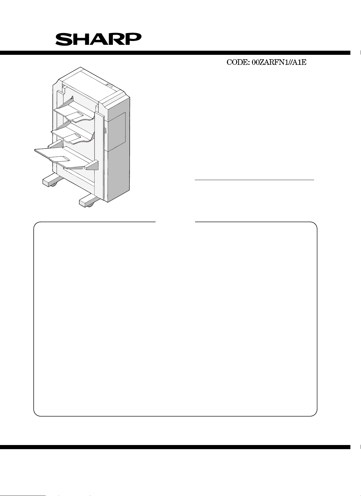
3-TRAY FINISHER
MODEL AR-FN1
CONTENTS
[ 1 ] BASIC SPECIFICATIONS . . . . . . . . . . . . . . . . . . . . . . . . . . . . . 1-1
[ 2 ] UNPACKING AND INSTALLATION. . . . . . . . . . . . . . . . . . . . . . 2-1
[ 3 ] PICTORIAL NOMENCLATURE . . . . . . . . . . . . . . . . . . . . . . . . . 3-1
[ 4 ] OUTLINE OF OPERATION . . . . . . . . . . . . . . . . . . . . . . . . . . . . 4-1
[ 5 ] DISASSEMBLY AND REINSTALLATION . . . . . . . . . . . . . . . . . 5-1
[ 6 ] ADJUSTMENT . . . . . . . . . . . . . . . . . . . . . . . . . . . . . . . . . . . . . . 6-1
[ 7 ] MAINTENANCE . . . . . . . . . . . . . . . . . . . . . . . . . . . . . . . . . . . . . 7-1
[ 8 ] TROUBLESHOOTING . . . . . . . . . . . . . . . . . . . . . . . . . . . . . . . . 8-1
[ 9 ] DESCRIPTION OF CIRCUITS. . . . . . . . . . . . . . . . . . . . . . . . . . 9-1
[10] CIRCUT DIAGRAM . . . . . . . . . . . . . . . . . . . . . . . . . . . . . . . . . 10-1
Parts marked with "! " is important for maintaining the safety of the set. Be sure to replace these parts with specified ones
for maintaining the safety and performance of the set.
This document has been published to be used
SHARP CORPORATION
for after sales service only.
The contents are subject to change without notice.
Page 2

CAUTION FOR BATTERY REPLACEMENT
(Danish) ADVARSEL !
Lithiumbatteri – Eksplosionsfare ved fejlagtig håndtering.
(English) Caution !
Dispose of used batteries according to manufacturer’s instructions.
(Finnish) VAROITUS
Paristo voi räjähtää, jos se on virheellisesti asennettu.
Vaihda paristo ainoastaan laitevalmistajan suosittelemaan
(French) ATTENTION
Il y a danger d’explosion s’ il y a remplacement incorrect
de la batterie. Remplacer uniquement avec une batterie du
même type ou d’un type équivalent recommandé par
Mettre au rebut les batteries usagées conformément aux
(Swedish) VARNING
Udskiftning må kun ske med batteri
af samme fabrikat og type.
Levér det brugte batteri tilbage til leverandoren.
Danger of explosion if battery is incorrectly replaced.
Replace only with the same or equivalent type
recommended by the manufacturer.
tyyppiin. Hävitä käytetty paristo valmistajan ohjeiden
mukaisesti.
le constructeur.
instructions du fabricant.
Explosionsfara vid felaktigt batteribyte.
Använd samma batterityp eller en ekvivalent
typ som rekommenderas av apparattillverkaren.
Kassera använt batteri enligt fabrikantens
instruktion.
Page 3
[1] BASIC SPECIFICATIONS
1. Type
Copier-fitted type (detachable)
2. Tray
1 Number of
trays
2 Type Top (tray 1) Normal tray
3 Number of
sheets
loadable
3
Middle (tray 2) Normal tray
Bottom (tray 3) Lift tray
Normal tray 500 (80 g/m
Lift tray 1500 (A4/11"
(A3/11"
3. Paper transfer
Center reference
4. Storage
Face-up/face-down
2
)
´ 8.5") 750
´ 17") (80 g/m
8. Lift tray
Off-set 30 mm
9. Staple unit
Paper discharge tray Lift tray
Storage Face-up
Number of sheets
that can be stapled
Paper size AB series A3, B4, A4, A4R, B5
2
)
Stapling reference 1 point (front)/ 1 point (far end)/ 2 points
Needle feed system Cartridge (5000 needles)
Detection No needle/no cartridge/stapler rotation
Service life more than 100 K
Manual mode None
50 sheets (80 g/m
25 sheets when the size is over A4/LT.
Inch series 11"
2
)
´ 17"/8.5" ´ 14"/
´ 13"/8.5" ´ 11"/
8.5"
8.5"
´ 11"R
10. Power supply
Supplied from copier (DC 24V, DC 5V)
5. Discharge size
Face-up Top A3 ~ A6R/11 ´ 17 ~ 8.5 ´ 5.5,
special paper
Middle A3
Bottom A3
Face-down Top A3
Middle A3
Bottom A3
~ A5/11 ´ 17 ~ 8.5 ´ 5.5
~ B5R/11 ´ 17 ~ 8.5 ´ 11R
~ B5/11 ´ 17 ~ 8.5 ´ 11R
~ B5/11 ´ 17 ~ 8.5 ´ 11R
~ B5R/ 11 ´ 17 ~ 8.5 ´ 11R
6. Paper weight
Face-up Top 52 ~ 128 g/m
Middle 56
Bottom 52 ~ 128 g/m
Face-down 56
* 1: Paper of 200g/m
For paper weight exceeding 105g/m
the paper size of A4/8.5"
~ 105 g/m
2
~ 176m2, can be used.
~ 105 g/m
2
, exceeded.
´ 11" or smaller can be used.
2
2
2
2
in the face up mode, only
7. Paper full detection
11. Power consumption
MAX 60W
12. Dimensions
590 (W) ´ 560 (D) ´ 998 (H)
13. Weight
About 50 kg
*
1
*
1
Top Provided
Middle Provided
Bottom Provided
1 – 1
Page 4
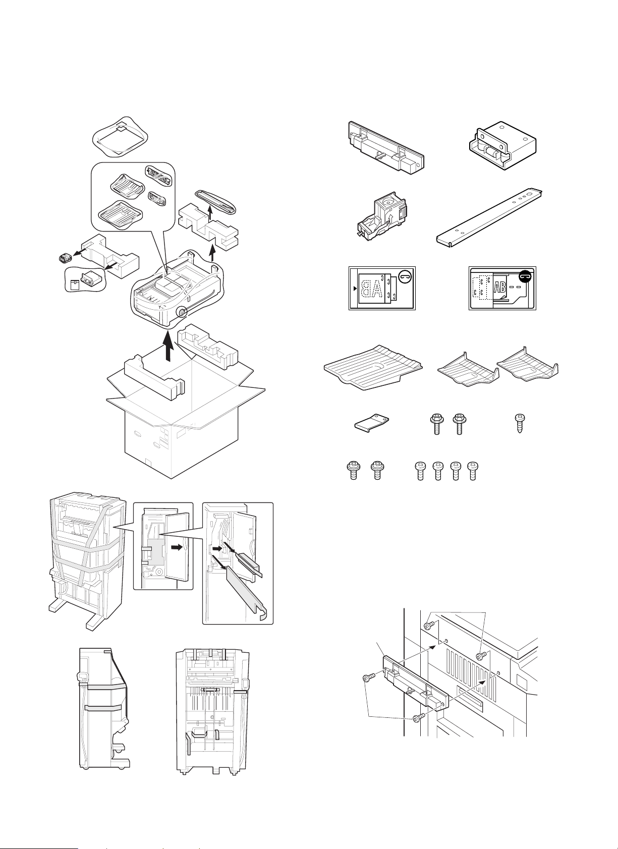
[2] UNPACKING AND INSTALLATION
1. Unpacking
Refer to the sketch below for unpacking.
2. Installation
Lock plate: 1
Staple cartridge: 1
Stapling position
label A: 1
Mounting plate: 1
Connecting plate: 1
Stapling position
label B: 1
Tray 3: 1 Exit trays: 2
Securing plate: 1 Screws A: 2 Screw B: 1
Screws C: 2
Screws D: 4
Unplug the copier’s power cord before carrying out
the following procedure.
1. Attach the lock plate and mounting plate.
Remove the two screws from the upper left cabinet of the copier and
attach the lock plate to the upper left cabinet using two screws D.
Screws for upper
left cabinet
Lock plate
2 – 1
Screws D
Page 5
· If the clearance is narrow at the upper part:
Turn knob A and knob B clockwise so that the clearances at the
upper part and lower part are uniform.
· If the clearance is wide at the upper part:
Turn knob A and knob B counterclockwise so that the clearances
at the upper part and lower part are uniform.
Knob BKnob A
Clearance
· If the connecting hole is displaced toward the front side:
Turn knob A counterclockwise so that the connecting hole matches
the guide pin.
Then, push the finisher into the copier.
If the clearance between the finisher and copier is not proper,
adjust the clearances at the upper part and lower part using procedure <1>.
(Top view)
Guide pin
Clearance
<2> If the guide pi n of the lock plate does not match the con-
necting hole of the finisher:
Turn the knobs at the lower part of the finisher to adjust the height.
· If the connecting hole is displaced toward the rear side:
Turn knob B counterclockwise so that the connecting hole matches
the guide pin.
Then, push the finisher into the copier.
If the clearance between the finisher and copier is not proper,
adjust the clearances at the upper part and lower part using procedure <1>.
(Top view)
Guide pin
Knob A
Knob B
7. Attach the exit tray and tray 3.
Insert the three pawls at the rear side of tray 3 into the holes of the
tray mounting platform and secure the tray using two screws.
Attach the two exit trays to the finisher from the boss at <1>.
2
1
Exit trays
Screws D
Pawl
Pawl
Tray 3
Pawl
Knob A
8. Attach the staple cartridge to the staple unit.
1 Turn the staple unit to face the front.
1
Knob B
2 – 3
Page 6
2 Insert the staple cartridge into the staple unit until it clicks in
place.
2
3 Return the staple unit to face down.
3
9. Paste the stapling position labels.
For document cover:
Stapling position label A
For ADF/RADF:
Stapling position label B
Connect the power cord, turn the main switch ON,
and perform the following procedure.
10. Check the finisher operation.
· Check the operation in the STAPLE SORT mode.
Make 10 sheets of copies in the STAPLE SORT mode.
Check to see if the copies are stapled properly.
For SPF:
Stapling position label A
11. Remove the tension spring of exit roller.
1) Pull out the exit unit of the copier until it stops.
2) Remove the 2 exit area cover securing screws and remove the
exit area cover.
3) Remove the 2 transport springs which are attached to the exit
area paper guide.
4) Store the 2 removed transport springs by hanging them on the exit
unit front frame (shown in Fig. 1).
5) Attach the exit area cover to its original position and secure it
using the 2 securing screws.
6) Insert the exit unit to the copier.
2 – 4
Page 7
Paper exit unit
Fixing screw
Paper exit cover
3)
2 – 5
Page 8
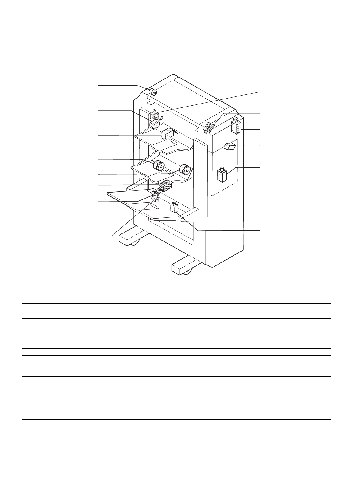
[3] PICTORIAL NOMENCLATURE
1. External view
3
4
1
5
No. Part name
1 Upper door
2 Front door
3 Tray 1
4 Tray 2
5 Tray 3
2
3 – 1
Page 9
2. Internal view
20
19
18
23
22
30
29
25
26
27
28
21
11
24
6
7
1
2
3
4
5
8
9
10
12
13
14
15
16
No. Part name
1 Paper discharge gate 1
2 Transfer follow-up roller 2
3 Vertical transfer roller 1
4 Transfer follow-up roller 1
5 Paper entry gate
6 Reversion paper discharge follow-up roller
7 Reversion paper discharge roller
8 Paper entry Shaft
9 Paper entry De-curler
10 Reversion gate
11 Reversion roller
12 Reversion pressure release roller
13 Short cut gate
14 S tray paper entry roller
15 Paper delivery pressure release roller
17
No. Part name
16 Paper discharge gate 3
17 Paper discharge roller 4
18 Paper discharge roller 3
19 S tray paper entry follow-up roller
20 Vertical transfer roller 3
21 Transfer follow-up roller 1
22 Paper discharge roller 2
23 Follower roller FIN
24 Paper discharge gate 2
25 Vertical transfer roller 2
26 Transfer follow-up roller 1
27 Paper discharge roller 1
28 Follower roller FIN
29 De-curler roller
30 Vertical transport roller 3 lower
3 – 2
Page 10
3. Clutch, solenoid
9. T12CL
13. PPSL
4. OG2SL
2. RRSL
10. PDCL
11. STORCL
5. OG3SL
12. T3ORSL
7. T3SLCL
3. OG1SL
14. STSL
1. INGSL
6. SPSL
8. T3UPSL
No. Signal name Name Function and Operation
1 INGSL Paper entry gate solenoid Switching between reversion/short cut path and outside turn path
2 RRSL Reversion roller pressure release solenoid Pressing reverse roller
3 OG1SL Paper discharge gate solenoid 1 Switching tray 1 paper delivery gate
4 OG2SL Paper discharge gate solenoid 2 Switching tray 2 paper delivery gate
5 OG3SL Paper discharge gate solenoid 3 Switching tray 3 paper delivery gate
6 SPSL Short path switching solenoid Switching short path gate
T3SLCL Tray 3 deceleration clutch Changing the speed of tray 3 paper speed change roller (Low
7
8 T3UPSL Tray 3 upper limit solenoid Pulling in tray 3 upper limit detection actuator
9 T12CL Tray 1 and 2 deceleration clutch
10 PDCL Puddler clutch Puddling in staple tray
11 STORCL ST paper delivery roller pressure release clutch Pressing staple paper delivery roller
12 T3ORSL Tray 3 paper exit roller clutch Changing the speed of tray 3 paper discharge roller (Low speed)
13 PPSL Paper holding solenoid Alignment of paper when stapling.
14 STSL Staple tray solenoid Holding the rear edge of paper in the staple tray.
speed)
Changing the speed of tray 1 and 2 paper delivery roller
(Low speed)
3 – 3
Page 11
4. Sensor
2. DSW2
1. DSW1
23. STND
27. READY
25. LSTS
13. T1PF
9. PFD3
14. T2PF
20. JGHP
10. PFD4
18. EVRE
19. OFHP
16. T3UP
8. PFD2
7. PFD1
5. INPD
3. DSW3
6. RVPD
21. PSHP
28. STID2
12. STPD
11. STID
15. T3OD
22. STUHP
17. T3DN
24. STHP
26. NCTS
Stapler unit
No. Signal name Name Function and Operation
1 DSW1 Copier connection switch Detecting the finisher attached to the copier
2 DSW2 Top door opening switch Detecting top door opening
3 DSW3 Front door opening switch Detecting front door opening
5 INPD Paper entry sensor Detecting paper entry
6 RVPD Reversion paper discharge sensor Detecting paper discharge
7 PFD1 Transfer detecting sensor 1 Detecting transfer 1
8 PFD2 Transfer detecting sensor 2 Detecting transfer 2
9 PFD3 Transfer detecting sensor 3 Detecting transfer 3
10 PFD4 Transfer detecting sensor 4 Detecting transfer 4
11 STID Staple tray paper entry sensor Detecting staple tray paper entry
12 STPD Staple tray paper sensor Detecting the presence of paper in staple tray
13 T1PF Tray 1 full sensor Detecting tray 1 filled with paper
14 T2PF Tray 2 full sensor Detecting tray 2 filled with paper
15 T3OD Tray 3 paper delivery sensor Detecting tray 3 paper delivery
16 T3UP Tray 3 upper limit sensor Detecting tray 3 upper limit
17 T3DN Tray 3 lower limit sensor Detecting tray 3 lower limit
18 EVRE Elevator motor encoder Elevator motor encoder
19 OFHP Offset motor home position detecting sensor Detecting offset motor home position
20 JGHP Jogger motor home position detecting sensor Detecting jogger motor home position
21 PSHP Pusher motor home position detecting sensor Detecting pusher motor home position
22 STUHP Staple UN movement motor home position
detecting sensor
23 STND Staple needle replacement sensor Detecting stapler rotation for the replacement of needles
24 STHP Stapler home position detecting sensor Detecting stapler home position
25 LSTS Staple detecting sensor Detecting the presence of needles in stapler
26 NCTS Stapler cartridge sensor Detecting the presence of stapler cartridge in stapler
27 READY Stapler self priming sensor Detecting needles in stapling position
28 STID2 Staple tray paper entry sensor 2 Detecting staple tray paper entry 2
Detecting staple UN movement motor home position
3 – 4
Page 12
5. Motor and PWB unit
2. RVM
1. FM
3. JGM
4. PSM
7. OFM
6. EVM
5. STUM
8. STM
9
10
11
No. Signal name Name Function and Operation Type
1 FM Main drive motor Transferring paper inside finisher DC brushless
2 RVM Reversion motor Reversing the paper DC stepping
3 JGM Jogger motor Positioning jogger to suit paper size and aligning paper in
staple tray
4 PSM Pusher motor Lowering the paper in staple tray to stapling position and lifting
the paper to delivery position
5 STUM Staple unit movement motor Moving staple unit to stapling position DC stepping
6 EVM Elevator motor Raising and lowing tray 3 DC brush
7 OFM Offset motor Shifting tray 3 back and forth to sort the paper in tray 3 DC brush
8 STM Staple motor Driving staple unit DC brush
9 Finisher main PWB 100/200 100/200V, Finisher control —
10 Filter PWB Common, Eliminating brush motor noise —
11 Filter PWB Common, Eliminating brush motor noise —
DC stepping
DC stepping
3 – 5
Page 13
[4] OUTLINE OF OPERATION
1. Transfer route
The 3-tray finisher’s transfer routes are as follows.
a. Tray 1 face-up paper discharge
c. Tray 2 face-up paper discharge
b. Tray 1 face-down paper discharge
2
d. Tray 2 face-down paper discharge
2
1
1
4 – 1
Page 14
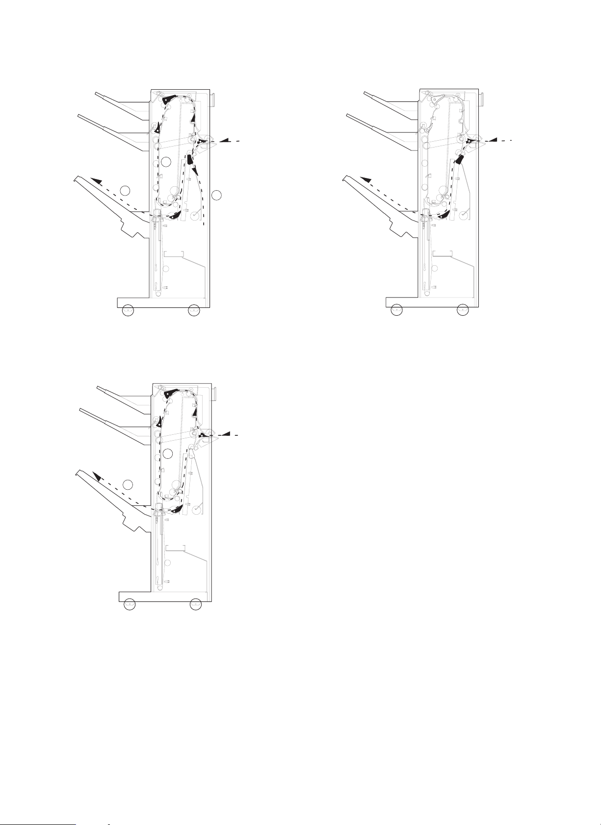
e. Tray 3 outside turn face-up paper discharge
2
g. Tray 3 chart-cut face-up paper discharge
3
f. Tray 3 outside turn face-down paper discharge
1
1
2
4 – 2
Page 15
2. Explanation of each section
The 3-tray finisher consists of (1)an upper paper transfer section, (2)a
reversion section, (3)a staple tray, (4)an offset tray, and (5)an elevator section.
It has the following functions: Paper discharge to a selected tray,
paper reversion, stapling for paper delivered to the offset tray (3
positions), offset, and elevation. Each function is performed according
to the mode instructed by the copier.
5) Trays 1 (10) and 2 (7) paper discharge operation
When paper is delivered to the trays 1 (10) and 2 (7) at a high-speed
in the 3 tray finisher, the trays 1 and 2 deceleration clutch (13) is
operated at paper delivery timing to decelerate the paper discharge
rollers 1 and 2 in order to align the paper to the trays 1 (10) and 2 (7)
with high accuracy.
6) Trays 1 (10) and 2 (7) paper full detection
Whether the trays 1 (10) and 2 (7) are filled with paper is detected by
the tray 1 and 2 paper full sensor.
1)
2)
4)
3)
5)
A. Upper paper transfer section
1) Paper transfer
By rotating the main driving motor (FM), the transfer rollers in the
finisher are driven.
The transfer speed is switched over between the copier speed mode
and the high-speed mode according to the paper discharge mode
and paper size.
2) Paper entry gate (4)
The paper entry gate (4) is operated by the paper entry solenoid(INGSL) to select the upper transfer (outside route) and reversion/short path according to the mode.
3) Paper discharge gate 1 (1)
The paper discharge gate 1 (1) is operated by the paper discharge
gate 1 solenoid (OG1SL), to select between the routes for paper
discharge to the tray 1 (10) and transport to the tray 2 (7)/staple tray.
4) Paper discharge gate 2 (8)
The paper discharge gate 2 (8) is operated by the paper discharge
gate 2 solenoid (OG2SL) to select between the routes for paper
discharge to the tray 2 (7) and transport to the staple tray.
(13)
(12)
(1)
(11)
(10)
(9)
(8)
(7)
Document reversion and
short-cut path
(6)
To stapler tray
No. Signal name Name
(1) — Paper discharge gate
(2) PFD2 Transfer detecting sensor 2
(3) PFD1 Transfer detecting sensor 1
(4) — Paper entry gate
(5) INPD Paper entry sensor
(6) PFD4 Transfer detecting sensor 4
(7) — Tray 2
(8) — Paper discharge gate 2
(9) T2PF Tray 2 paper full detecting sensor
(10) — Tray 1
(11) PFD3 Transfer detecting sensor 3
(12) T1PF Tray paper full sensor
(13) TI2CL Trays 1 and 2 deceleration clutch
(2)
(3)
(4)
(5)
4 – 3
Page 16
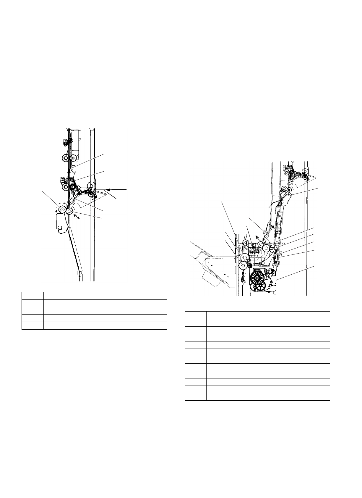
B. Reversion unit
1) Reversion motor (RVM)
The reversion motor is connected to the reversion roller (4).
The paper is pulled into the reversion path by the reversion motor
rotating in forward, and fed into the upper transfer route by the motor
rotating in reverse. When the paper is discharged through the shortpath, its transfer is performed by the reversion roller (4) until the
paper enters the staple tray.
2) Reversion pressure release roller
The reversion pressure release roller (3) is pressure released or pressurized through ON/OFF control of the reversion roller pressure release solenoid, to achieve the reversion of the paper at a high speed
without reducing JOB efficiency.
(1st sheet is reversed
and discharged.)
(1)
5) Short path switching gate (1)
The short path switching gate (1) is operated by the short path
switching solenoid (SPSL), to select the short path to feed paper to
the reversion path and stable tray.
6) Staple tray paper discharge
When the paper delivery roller pressure release clutch (STORCL) is
turned ON, the paper delivery pressure release roller (4) is pressurized through the cam to discharge the paper from the stable tray.
7) Paper discharge gate 3 (5)
The paper discharge gate 3 (5) is operated by the paper discharge
gate 3 solenoid (OG3SL) to switch over the routes of paper inside the
staple tray between the paper discharge side and the staple side of
the off-set tray.
8) Tray 3 deceleration clutch (8)
Tray 3 paper exit roller clutch (2)
The paper discharge rollers 3 and 4 are speed changed to improve
the stackability of stapled paper being discharged to the off-set tray.
(4)
Entry
Discharged
Pressure
release
No. Signal name Part name
(1) RVPD Reversion paper delivery sensor
(2) — Reversion gate
(3) — Reversion pressure release roller
(4) — Reversion roller
(2nd sheet is reversed
and entered.)
(2)
(3)
C. Staple tray
1) Jogger motor (JGM)
The jogger motor is driven when the paper is fed into the staple tray,
to operate the jog plates F and R so as to align the sidewise edge of
the paper.
2) Puddler (11)
The puddler clutch (PDCL) is turned ON when the paper is fed into
the staple tray, to give the puddler a full turn so as to drop the paper
downward (pusher), thus achieving alignment in the vertical direction.
3) Pusher motor (PSM)
With the pusher motor rotating, the paper stored inside the staple tray
is lowered from the home position (discharge position) to the stapling
position; after stapling, the paper inside the staple tray is elevated
from the stapling position to the home position.
4) Staple unit movement motor (STUM)
The staple unit is moved to the stapling positions (front, far end, 2
centers) by the staple unit motor.
(2)
(11)
(10)
(9)
(8)
No. Signal name Part name
(1) — Short path switching gate
(2) T3SLCL Tray 3 speed reduction clutch
(3) — Tray 3 speed reduction clutch
(4) — Paper delivery pressure release roller
(5) — Paper discharge gate 3
(6) STPD Staple tray paper detection sensor
(7) — Staple unit
(8) T3ORSL Tray 3 paper exit clutch
(9) T3OD Tray 3 paper delivery sensor
(10) STID Staple tray paper entry sensor
(11) — Puddler
(1)
(3)
(4)
(5)
(6)
(7)
4 – 4
Page 17
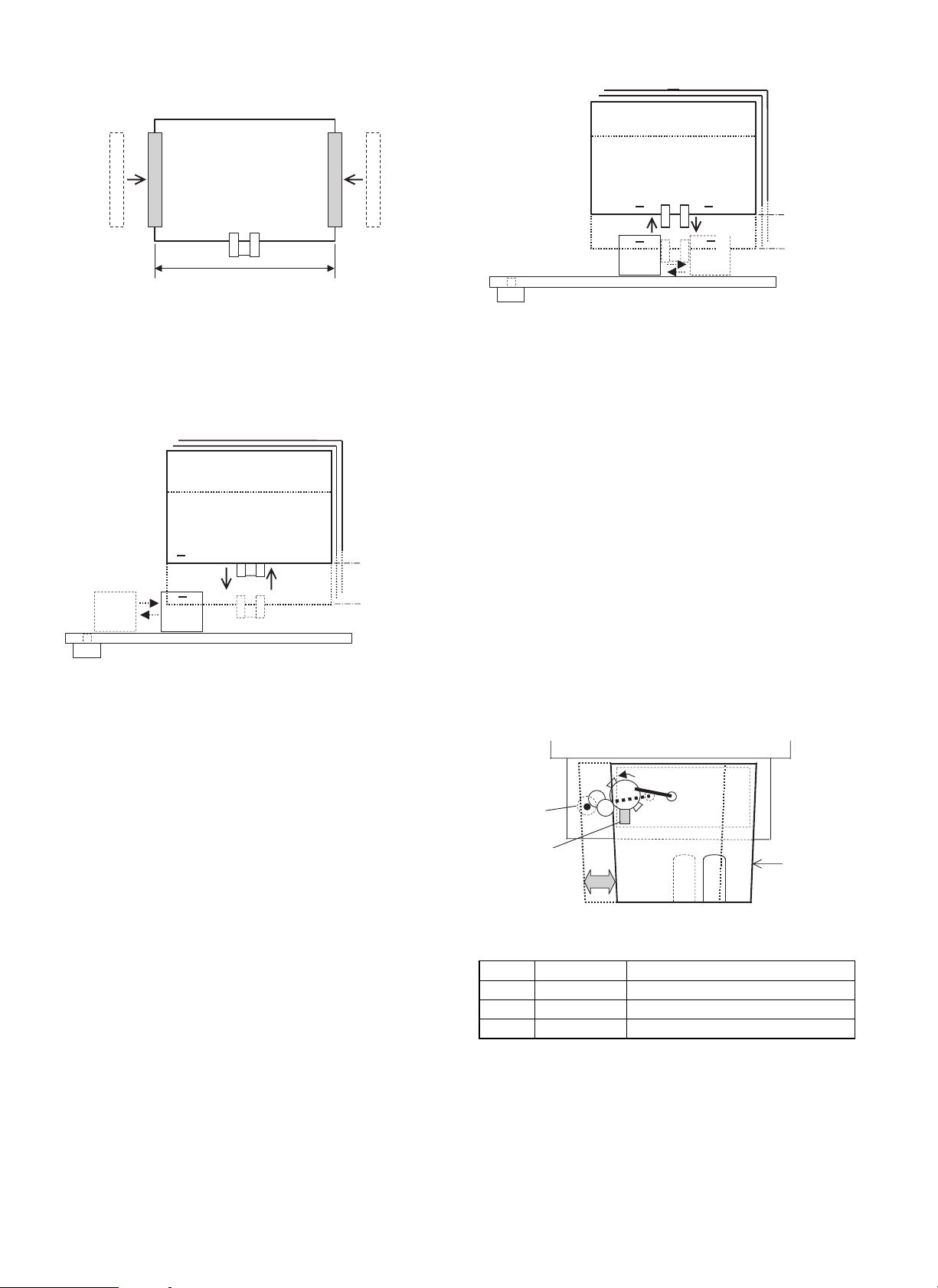
(Operation of stapling)
1) 2) 2) 1)
Jog plate
R
Pusher
Paper size
Jog plate
F
Jogging in lateral direction
1) The jog plates are moved to the stand-by position before the
paper is fed to the staple tray.
2) Immediately after the paper is fed into the staple tray, the jog plate
is moved to the paper size position to ensure the alignment of the
paper.
Staple unit
Home
position
Staple unit moving
motor
Pusher
2) 4)
3)
1)
5)
Paper discharge
position
Staple position
ST rail
Staple unit movement at the time of stapling (1-point
stapling)
1) The stapler unit is moved to the stapling position.
– The number of sheets to be stapled is fed to the staple tray –
2) The pusher (the sheets to be stapled) is lowered the stapling
position.
3) The paper is stapled ... (in the case of 2-point stapling, the action
that is described on the following page is added.)
4) The pusher (the sheets stapled) is elevated to the paper discharge position.
5) After the job, the stapler unit is returned to the home position.
Pusher
Staple unit
moving range
Staple position
ST rail
Staple unit moving
motor
1)
3)
4)
5)
2)
Stapler unit movement at the time of stapling
(2-point stapling action is added.)
1) The pusher is elevated to the position which makes it possible for
the staple unit to move.
2) The staple unit is moved to the staple position where the 2nd
staple is driven.
3) The pusher (sheets to be stapled) is lowered to the stapling position.
4) Sheets are stapled.
5) The staple unit is returned to the 1st staple position.
(After the job is finished, the staple unit is returned to the home
position.)
D. Off-set tray
1) Off-set motor (3)
When the off-set motor (3) is driven, the tray is shifted sidewise
against the direction in which the sheets are delivered, so that the
sheets discharged into the off-set tray (1) are sorted by the specified
number of sheets. The rotation is unidirectional and controlled by the
crank. The motor is braked to a stop by the off-set home position
sensor (2) turning ON.
(3)
(2)
Moving range
(30 mm)
(1)
4 – 5
No. Signal name Part name
(1) — Tray 3 (Off-set tray)
(2) OFHP OFHP Off-set home position sensor
(3) OFM Off-set mo tor
Page 18
E. Elevator
1) Elevator motor (3)
When the elevator motor (3) is driven, the winding pulley (5) is rotated
in both forward and reverse to wind up the wire (6) stretching vertically so that the tray 3 (off-set tray) is moved up and down. This
allows the discharge of paper at a fixed position according to the
number of sheets to be loaded on the off-set tray.
2) Off-set tray full and load detection
When the power is turned ON, the off-set tray lowers to the lower limit
sensor (4) position. Then it elevates until the upper limit sensor (7)
turns ON, while counting the encoder pulses of the elevator motor (3).
The volume of paper loaded on the off-set tray is calculated (0 100%) by counting the number of pulses from the elevator encoder
(1).
The off-set tray is judged to be full when both the lower and upper
limit sensors (4, 7) are turned ON.
3) Upper limit sensor solenoid (T3UPSL)
When the paper is discharged from the off-set tray, the upper limit
sensor solenoid is turned on to pull in the actuator so that the sheet
discharged does not ride on the actuator of the upper limit sensor (7).
(7)
3. Basic operation
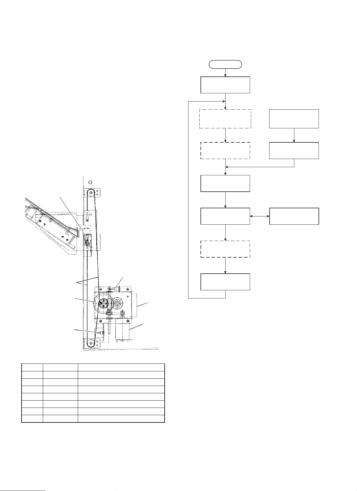
A. Basic operation flowchart
Power ON
Initialization when
powered on
Independent movement
of staple unit
(Staple position)
Independent shifting
(Offset tray)
JOB_START
Operation when
JAM error occurs
Operation when
door is closed
(1)
(6)
(5)
(4)
No. Signal name Part name
(1) — Elevator motor encoder
(2) — Elevator drive unit
(3) EVM Elevator motor
(4) T3DN Tray 3 lower limit sensor
(5) — Winding pulley
(6) — Wire
(7) T3UP Tray 3 upper limit sensor
(3)
(2)
Transfer
Off-set trail paper
discharge
JOB_END
Fig. 1 Basic operation flowchart
Stapling
1) Initialization
The finisher is initialized (home positioning of each motor) at the
following timing.
· When the power is turned on.
· The finisher leaves the copier and when either of the top or bottom
door is opened.
· When the copier start key is pressed (JOB_START):
· Recovery action is performed.
4 – 6
Page 19
[5] DISASSEMBLY AND REINSTALLATION
[Note]
· This section explains the procedure for disassembling and rein-
stalling the unit. Reinstall the unit in the reverse order of disassembly.
· Disassemble the unit in numerical order in each sketch.
· This section covers the procedure for disassembling the following
major parts. For the other parts, refer to the Parts Guide.
No. Part name
1 Main drive motor
2 Staple unit movement motor
3 Reversing motor
4 Elevator motor
5 Off-set motor
6 Stapler
7 Jogger motor
8 Pusher motor
9 Elevator wires, top and bottom
10 Paper discharge roller 3
1. Main drive motor
2. Staple unit movement motor
1)
1)
3)
2)
1)
2)
1)
2)
3)
5)
5)
6)
1)
4)
5)
4)
4)
5 – 1
Page 20

3. Reversion motor 4. Elevator motor
3)
2)
1)
1)
4)
1)
1)
2)
2)
3)
(A)
1)
4)
5)
6)
5)
5)
4)
5)
5)
5)
[Note] Before trying to remove the frame stay 6), make sure the tray
3 is at the upper limit position.
If the tray 3 is not at the upper limit position, turn the knurled
part on the shaft A in the sketch and move the tray 3 to the
upper limit.
7)
7)
7)
5 – 2
7)
7)
Page 21

9)
11)
12)
13)
5. Off-set motor
1)
2)
8)
10)
8)
14)
8)
13)
6)
4)
3)
5)
8)
A
9)
B
15)
7)
6)
[Note] When the setting the tray 3 cover (bottom), use caution not to
get the wire caught in the harness B.
When setting the off-set motor 9), pay attention to the filter
PWB A. For the direction, see the sketch given above.
16)
A
[Note] When setting the elevator motor 16, pay attention to the direc-
tion of the filter PWB A. For the direction, see the sketch
given above.
5 – 3
Page 22

6. Stapler
6)
5)
5)
10)
2)
9)
3)
1)
7. Jogger motor
1)
8)
7)
2)
5 – 4
Page 23

4)
4)
3)
3)
6)
3)
5)
3)
3)
3)
6)
3)
3)
3)
3)
5)
[Note] When installing the jogger motor 6), pay attention to the har-
ness pulling-out direction. See the sketch given above.
8. Pusher motor
1)
2)
8)
5)
7)
7)
5 – 5
Page 24

9. Elevator wires, top and bottom
6)
11)
4)
2)
2)
3)
(A)
1)
1)
7)
5)
5)
7)
8)
7)
4)
5)
5)
10)
12)
13)
10)
10)
13)
12)
7)
7)
[Note] If the tray 3 is not at the upper limit position, turn the knurled
part on the shaft A in the sketch and move the tray 3 to the
upper limit position.
8)
8)
9)
8)
8)
8)
[Note] Remove the two screws 13) and:
1) Move the off-set tray to the lower limit position.
2) Turn the knurled part on the elevator worm gear shaft under the
elevator drive box so that the D-cut surface on the winding pulley
points upward.
C
14)
17)
15)
A
18)
16)
B
[Note] Remove the elevator wires (top, bottom) at the rear frame
5 – 6
side in the same manner.
Page 25

[Reinstalling elevator wires (top, bottom) at the front
frame side]
1) Insert both the top elevator wire 15) and bottom elevator wire 16)
into the elevator pulley drive shaft A. Secure the winding pulley
18) with the screw 17).
2) Hook the bottom elevator wire 16) on the lower wire roller B from
the left side of the winding pulley 18), without giving extra winding.
With the wire extended upward, hook the wire mounting spring 14)
on the wire hook.
3) Wind the top elevator wire 15) onto the winding pulley 18) 3 and
3/4 turns in the clockwise direction, and hook on the upper wire
roller C. Hold it stretched downward.
4) When setting the top and bottom elevator wires at the rear frame
side (see the sketch below), observe the following conditions:
[Note] Observe the following conditions when setting elevator-wires
(top and bottom) at the rear frame side. See the sketch below.
· The bottom elevator wire 16) should be hooked onto the
bottom wire roller B from the right side of the winding pulley
18) without giving extra winding.
· The top elevator wire 15) should be wound onto the winding
pulley 18) 3 and 3/4 turns in the counterclockwise direction.
10. Paper discharge roller 3
10-1. Paper discharge roller 3 (top)
5)
3)
1)
5)
2)
1)
6)
4)
5)
4)
5)
15)
16)
14)
18)
C
17)
2)
8)
7)
7)
A
9)
B
10)
9)
5 – 7
Page 26

A
11)
7)
12)
7)
A
[Note] After removing the E-ring 11), slide the bearing A in the direc-
tion A to remove the paper discharge roller 3 12).
11) 12)
10-2. Paper discharge roller 3 (bottom)
1)
2)
4)
5)
3)
9)
D
A
B
8)
D
3)
6)
6)
B
[Note] After removing the E-ring 8), slide the bearing A in the direc-
tion A to remove the paper discharge roller 4 9).
[Caution to be taken wh en rein stalling ]
When reinstalling the paper discharge roller 4, make sure that the
lock screw C settles in the U-shape notch D in the clutch B.
5 – 8
A
8)
9)
Page 27

[6] ADJUSTMENT
The following table shows the main parts requiring adjustment at the
time of replacement
Item Part name
1 Jogger F/R
2 Paper entry gate solenoid
3 Reversion roller pressure release solenoid
4 Paper discharge gate solenoid 1
5 Paper discharge gate solenoid 2
6 Paper discharge gate solenoid 3
7 Short path switching solenoid
8 Tray 3 upper limit solenoid
9 Paper holding solenoid
10 Paddler clutch
11 Vertical transport roller 3 intermediate unit
12 Paper entry port de-curler unit
Note: Remove or install parts in numerical order shown in the follow-
ing figures.
1. Jogger F/R
A. Let the unit staple 5 sheets of A4 or letter paper and check the
bundle of the sheets for deviation in directions A).
Condition Adjusting procedure
1 When the deviation in the
direction A) exceeds 1 mm.
Note: The width between joggers can be visually checked by observ-
ing the label inside the staple tray.
Jogger
Decrease the simulation value.
(Decreasing the simulation by
1 narrows the width between
the joggers by 0.63 mm.)
Increase the simulation value.
(Increasing the simulation value
by 1 widens the width between
the joggers by 0.63 mm)
Label
A)
Pin
B. When the deviation in directions A) is are within 1 mm, there is no
need to adjust the jogger F/R.
C. When the deviation exceeds 1 mm, adjust the jogger F/R accord-
ing to the simulation 3-6: Adjusting Finisher Jogger Position.
Letter position
A
Jogger
A4 position
The spacing between
labels is 0.5 mm.
Sim. 3-6: Adjusting Finisher Jogger Position
The screen above is displayed after the sub number of the simulation
is entered.
1) Adjust the value with the numeric keypad.
2) The joggers in the finisher are operated by pressing the [EXECUTE] key. The [EXECUTE] key is displayed in reverse video
during loading operation. When the [EXECUTE] key in this state
is pressed, loading operation can be canceled.
6 – 1
Page 28

2. Paper entry gate solenoid
[Adjustment and precaution in setting]
2)
2)
3)
1)
2)
1)
2)
Positioning mark
8)
P
Q
View looking from P
B
A
View looking from Q
1) Insert the paper entry gate solenoid pin A into the hole B on the
paper feed gate arm and secure with the screw 4). In this step,
align the F flame edge with the position aligning stamp as shown
in the enlargement above.
2) When setting the paper entry gate solenoid spring 8), ensure that
the direction of the spring hook is as shown in the figure.
5)
6)
4)
7)
3. Reversion roller pressure release
solenoid
2)
1)
2)
3)
6 – 2
Page 29

4. Paper discharge gate solenoid 1
3)
1)
6)
7)
5)
4)
[Precaution in setting]
1) Insert the solenoid pin B through the slot A in the paper feed lever,
insert the shaft C through the D-cut hole in the paper feed lever,
and secure the solenoid with the screw 4). In this step, align the
edge of the gate solenoid installation plate with the position aligning stamp as shown in the enlargement below.
C
2)
2)
2)
1)
2)
A
B
5)
4)
Positioning marks
6)
7)
4)
6 – 3
Page 30

[Adjustment and precaution in setting]
1) Insert the solenoid pin A through the longer slot in the valve
moving arm B shown in the figure below and secure with the
screw 4). In this step, align the edge of the solenoid installation
plate 6) with the position aligning stamp as shown in the enlargement.
2) Hook one end of the paper discharge solenoid spring C in the
smaller slot in the valve moving arm B and the other end in the
hole in the F flame.
B
A
6)
5)
6)
C
Positioning lines
Match the right-most with the
middle of the second.
5. Paper discharge gate solenoid 2
4)
4)
[Adjustment and precaution in setting]
1) Insert the solenoid pin A through the longer slot in the paper
discharge gate 2 B and secure with the screw 4). In this step, the
solenoid installation plate 6) is positioned as shown in the enlargement below.
7)
B
A
4)
2)
2)
Positioning mark
1)
3)
6 – 4
Page 31

6. Paper discharge gate solenoid 3
7. Short path switching solenoid
2)
2)
7)
1)
6)
3)
5)
4)
1)
2)
3)
4)
[Adjustment and precaution in setting]
1) Insert the solenoid pin B through the notch in the manual stopper
rotation arm A and secure with the screw 4). In this step, align the
edge of the solenoid installation plate 6) with the positioning line at
the center.
A
B
4)
11)
3)
3)
3)
3)
10)
6 – 5
Page 32

8. Tray 3 upper limit solenoid
[Adjustment and precautions in setting]
1) Adjust the distance from the end A of the installation plate 6) to
the actuator B for 8 mm, with the solenoid fully pulled. Secure the
solenoid with the screw 4).
8mm
AB
C
P
Slide the upper limit sensor unit 2) in the direction indicated by the
arrow and remove it.
1)
2)
D
As a rough guide, screw so
that the edges of solenoid
mounting plate 6) are
matched.
Line
2) Use caution to align the notch C of the upper limit sensor unit 2
with the notch D of the rear edge reinforcement plate when securing the upper limit sensor unit 2 with the screw 1). (See the figure
below.)
4)
6)
4)
3)
6)
5)
6 – 6
Page 33

9. Paper holding solenoid
10. Paddler clutch
2)
2)
1)
3)
2)
2)
1)
3)
[Adjustment and note for setting]
Adjust the guide solenoid fixing plate so that the staple tray guide is in
contact with the solenoid fulcrum arm.
Staple
movable
PG
[Adjustment and note for setting]
Adjust the paddler adjustment plate so that the paddler tip enters the
clearance of the staple tray guide.
6 – 7
Paddler
Page 34

11. Vertical transport roller 3 intermediate
unit
Insert the jig between the de-curler roller and the de-curler follower
shaft of the vertical transport roller 3 intermediate unit, and install it.
Set values
Without paper entry
port de-curler unit
Nip amount 1.3
Shaft dimension 20.8 21.6
Jig
± 0.1 0.5 ± 0.1
De-curler jig R 1.3 De-curler jig R 0.5
De-curler jig F 1.3 De-curler jig F 0.5
[Process]
1) Temporarily install the vertical transport roller 3 intermediate unit
and the de-curler follower shaft to the machine.
2) Insert de-curler jigs F and R between the de-curler roller and the
de-curler follower shaft. While gently pressing the jigs downward,
tighten the fixing screw to fix the jigs.
3) Check that the de-curler jig R enters between the front side and
the rear side of the shaft.
4) If the jig R does not enter smoothly, repeat the above procedures
and check again.
De-curler follower shaft
De-curler roller
With paper entry
port de-curler unit
Fixing screw
Fixing jig R
Rear side Front side
R1.3
De-curler jig R1.3 De-curler jig F1.3
F1.3
Fixing screw
Fixing jig F
R0.5
De-curler jig R0.5
De-curler jig F0.5
6 – 8
Page 35

12. Paper entry port de-curler unit
· Nip amount adjustment
For the paper entry de-curler unit, adjust the nip amount of the
de-curler roller according to the destination as shown below.
Nip amount 0.5 ± 0.1 0.8 ± 0.1 1.2 ± 0.1 1.6 ± 0.1
(Reference) Shaft
dimension
Inch series F/R
EX AB series F R
Japan F/R
· Adjustment procedure
The nip amount adjustment is made with the paper entry de-curler
jig.
1) Insert the jig to fit the inscribed mark of each nip amount as
shown in he figure below.
2) Press the de-curler adjustment plate F (arrow section) until the
shaft is in contact with the jig.
3) Tighten the screw.
Perform the same procedure to the front side and the rear side.
21.6 21.3 20.9 20.5
Front side insertion position
De-curler adjustment plate F (R)
Paper entry de-curler
follower shaft
3
Screw tightening (M4x8, 3 pcs.)
Hold th section.
2
Paper entry de-curler
Insert
Rear side insertion position
Paper entry de-curler
1
jig
6 – 9
Page 36

[7] MAINTENANCE
If reception is performed during maintenance work, it is very dangerous. Therefore, be sure to disconnect the power cable from the machine.
1. Maintenance system table
| : Cleaning ★:
Lubrication
Name Work
Rollers Clean Maintenance service 80K or 2 years
Paper guides Clean Maintenance service 80K or 2 years
Gears Lubricate Grease Maintenance service 80K or 2 years
Belts Check Maintenance service 120K or 2 years
Sensors Check Maintenance service 80K or 2 years
Staple unit Replace Maintenance service 100K
✕: Check (Clean, replace, or adjust according to necessity.)
Execution conditions
Execution timing Cycle
Note
7 – 1
Page 37

(Rollers/Paper guides)
C
C
D
E
F
B
A
A
B
E
D
F
7 – 2
Page 38

K
K
G
H
J
L
G
I
H
I
L
J
7 – 3
Page 39

(Gears)
Others (Sensors) (Belts)
7 – 4
Page 40

[8] TROUBLESHOOTING
1. Trouble code
Trouble code
Main
code
Sub
code
F1 00 Content Finisher communication trouble
Detail Communication line test error occurs
when power is turned on or after the exit
of a simulation mode.
Improper communication with sorter
Cause Improper connection or broken wire of
Check
and
remedy
01 Content Finisher jogger shift trouble
Detail Jogger shift trouble
Cause Motor lock
Check
and
remedy
02 Content Finisher transport motor error
Detail Transport motor drive trouble
Cause Motor lock
Check
and
remedy
04 Content Finisher indexer lower limit detected
Detail Indexer has exceeded lower limit.
Cause Sensor defective
Check
and
remedy
05 Content Finisher elevator motor trouble
Detail Indexer has exceeded upper limit
Cause Sensor defective
Check
and
remedy
06 Content Finisher shift motor error
Detail Finisher shift motor trouble
Cause Motor lock
Check
and
remedy
connector or harness between copier
and Finisher
Finisher control PWB defective
Control PWB (PCU) defective
Malfunction due to noise
Clear by turning the power supply
OFF/ON.
Check communication line connector and
harness.
Replace Finisher control PWB or PCU
PWB.
Motor rpm abnormality
Motor overcurrent
Finisher control PWB trouble
Check the jogger motor operation with
SIM 3-3.
Check transport motor operation with
SIM3-3.
Finisher control PWB defective
Check sensor with SIM3-2.
Finisher control PWB defective
Check sensor with SIM3-2.
Improper motor speed
Overcurrent to motor
Finisher control PWB defective
Check shift motor operation with SIM3-3.
Description
Trouble code
Main
code
Sub
code
F1 08 Content Finisher staple shift motor trouble
Detail Staple motor drive trouble
Cause Motor lock
Check
and
remedy
10 Content Staple unit operation trouble
Detail Staple operation trouble
Cause Motor lock
Check
and
remedy
11 Content Pusher motor trouble
Detail Pusher motor trouble
Cause Motor lock
Check
and
remedy
15 Content Finisher elevator motor trouble
Detail Elevator motor trouble
Cause Motor lock
Check
and
remedy
80 Content Finisher power trouble
Detail 24V power is not supplied to the finisher
Cause Connector harness improper connection
Check
and
remedy
Motor RPM abnormality
Motor overcurrent
Finisher control PWB trouble
Check the staple motor operation with
SIM 3-3.
Motor rpm abnormality
Motor overcurrent
Finisher control PWB trouble
Check the staple motor operation with
SIM 3-3.
Motor rpm abnormality
Motor overcurrent
Finisher control PWB trouble
Check the pusher motor operation with
SIM 3-3.
Motor rpm abnormality
Motor overcurrent
Finisher control PWB trouble
Check the elevator motor operation with
SIM 3-3.
PWB.
or disconnection
Finisher control PWB trouble
Power unit trouble
Check the sensor operation with SIM 3-2.
Description
8 – 1
Page 41

(1) Finisher does not operate. (excluding JAM
state)
1
2
Is connection
cable properly
connected?
Is load on motor
shaft normal?
CNA-6 and CNA-5 of
Is motor winding
(between U, V, and W)
CNA-1 and CNA-3 of
connected normally?
signals of main PWB
Motor rotates
even slightly?
YES
YES
+5V between
main PWB?
YES
shorted?
NO
+24V between
main PWB?
Is harness
YES
YES
Are
DSW1, 2, 3
OK?
YES
NO
Connect connection
cable to body properly.
Check mechanical load
NO
and driving system.
Remove foreign matter.
NO
Check or replace harness
or check supply voltage.
YES
NO
NO
Replace motor.
NO
Check or replace harness
or check supply voltage.
Connect harness
Check connections.
Check harnesses at
upper and lower surfaces
NO
and harness leading to
upper transfer switch for
Is voltage
connections, and replace
applied to motor
connector?
properly.
if necessary.
NO
Staple unit
moving motor rotates
normally?
YES
Pusher motor rotates
normally?
YES
Jogger motor rotates
normally?
YES
Check main PWB and
replace if necessary.
NO
NO
NO
4
4
4
YES
Transfer motor
rotates normally?
YES
Is motor
encoder output
normal?
Elevator motor
YES
rotates normally?
YES
Check main PWB and
replace if necessary.
Off-set motor
rotates normally?
YES
NO
2
NO
Check motor and
replace if necessary.
NO
3
NO
3
YES
8 – 2
Page 42

(2) Transfer motor error (3) Elevator and off-set moter error
2
Is load on motor
shaft normal?
YES
Is motor winding
(between U, V, and W)
shorted?
NO
Is harness
connected normally?
YES
Check mechanical load
NO
and driving system.
Remove foreign matter.
YES
NO
Replace motor.
Connect harness
properly.
3
Is fuse blown out?
YES
Is load on motor
shaft normal?
YES
Is motor winding
shorted?
NO
NO
NO
YES
Replace fuse.
Check mechanical load
and driving system.
Remove foreign matter.
Replace motor.
Motor rotates
even slightly?
YES
Is motor
encoder output
normal?
YES
Check main PWB and
replace if necessary.
NO
NO
replace if necessary.
Is voltage
applied to motor
connector?
YES
Check motor and
NO
Is harness
connected normally?
YES
Motor rotates
even slightly?
YES
Is motor
encoder sensor output
normal?
YES
NO
NO
NO
Connect harness
applied on motor
Check motor and
replace if necessary.
Replace sensor
mounting and replace
Check harness and
replace if necessary.
properly.
Is voltage
connector?
YES
if necessary.
NO
8 – 3
Check main PWB and
replace if necessary.
Page 43

(4) Stepping moter error
(6) Clutch and solenoid error
4
Is load on motor
shaft normal?
YES
Is motor winding
shorted?
NO
Is harness connected
normally?
YES
Check mechanical
NO
load and driving system.
Remove foreign matter.
YES
NO
Replace motor.
Connect harness
properly.
6
Is each
load properly
mounted?
YES
Conduction
between coils of each
load?
YES
Conduction
between connectors and
terminals?
YES
NO
Check mounting and
replace if necessary.
NO
NO
Replace clutch or
Check harness and
replace if necessary.
solenoid.
Check main PWB and
replace if necessary.
(5) Sensor error
5
Is sensor
mounted properly?
Is harness connected
properly?
Replace main PWB.
YES
Check sensor mounting
NO
and harness and replace
if necessary.
Replace main PWB.
8 – 4
Page 44

[9] DESCRIPTION OF CIRCUITS
1. Outline
The finisher main circuit transmits and receives data to and from the copier main PWB. According to instructions from the copier, it controls loads,
sensors and the input of switching information.
The finisher main circuit consists of a circuit which receives signals from sensors and switches, a circuit which drives solenoids and clutches, CPU,
ROM, expansion I/O and other peripheral circuits.
2. Block diagram
The finisher block diagram is shown in Fig. 1.
Copier
Jogger motor HP sensor
Stapler self-priming sensor
Pusher motor HP sensor
Staple unit HP sensor
Tray 2 paper full sensor
Stapler needle
replacement sensor
Elevator motor encoder
Off-set HP sensor
Staple HP sensor
Transfer motor encoder
Paper entry sensor
Reversion paper discharge sensor
Transfer detection sensor 1
Transfer detection sensor 2
Transfer detection sensor 3
Transfer detection sensor 4
Tray 3 paper discharge sensor
Staple tray paper entry sensor
Staple paper detection sensor
Tray 1 paper full sensor
Staple tray paper entry sensor 2
Tray 3 upper limit sensor
Tray 3 lower limit sensor
Staple needle detection sensor
Staple cartridge sensor
Copier connection
switch
Upper door switch
Front door switch
BUFF
IC14
+5V
GND1
GND2
10V generating
circuit
ZD1,7,Q5
JGHP
READY
PSHP
STUHP
T2PF
STND
EVRE
OFHP
STHP
FMRE
INPD
RVPD
PFD1
PFD2
PFD3
PFD4
T3OD
STID
STPD
T1PF
STID2
T3UP
T3DN
LSTS
NCTS
+24VIN
Level
conversion
circuit
ZD3,4,5,6
F-RES
X1
[Mode 1]
+24VIN
IC19
+24V
F-TXD
F-RXD
F-DTR
F-DSR
F-RES
8MHz
"1"
"0"
"0"
PWD
DSW1
DSW2
DSW3
+10V
RXD0
TXD0
P95
P94
/RES
XTAL
EXTAL
MD0
MD1
MD2
P70
P71
P72
P74
P75
P77
P80
P81
PA0
PA6
EXPA0
EXPA1
EXPA3
EXPA4
EXPA5
EXPA6
EXPA7
EXPB0
EXPB1
EXPB2
EXPB3
EXPB4
EXPB5
EXPB6
EXPB7
EXPG0
‚d‚w‚o‚f‚O
EXPG1
EXPG2
EXPG3
RES
CPU(H8/3040)
IC2
EXP(M66500F)
IC3
PA4
PA7
P44
P 45
PB0~3
P40~43
PB4~7
P60
P46 PPSL
P47 STSL
A0~16
D0~7
CS0
RD
WR
CS2
CS
WR
RD
D0~7
A0~2
EXPE4
EXPE5
EXPE0
EXPE1
ECPC0~3
EXPF0
EXPF1
EXPF2
EXPF3
EXPF4
EXPF5
EXPF6
EXPF7
EXPC4
EXPC5
EXPC6
EXPC7
+10V
FMPWM
FMDIR
OFMA
OFMB
: A,B,A/,B/
*
RM*
STUM*
PM*
PMPD
A0~16
D0~7
ROMCS
RD
WR
EXPCS
EXPCS
WR
RD
D0~7
A0~2
STMA
STMB
EMA
EMB
JM*
INGSL
T3UPSL
OG1SL
OG3SL
RRSL
T30RCL1
PDCL
STORCL
SPSL
T12CL
OG2SL
T3SLCL
PPSL
STSL
2-phase brushless
motor driving circuit
DC brush motor
4
2-phase stepping
motor constant-current
2-phase stepping
4
motor constant current
4
2-phase stepping
motor constant current
17
8
DC brush motor
driving circuit(H driver)
DC brush motor
driving circuit(H driver)
4
2-phase stepping
motor constant current
driving circuit IC8
Solenoid/
Solenoid/
IC10,16,20
driving circuit
IC1
driving circuit
IC4
driving circuit
IC7
driving circuit
IC11
ROM(1M)
A0~16
D0~7
CS
OE
IC6
IC9,Q1,2,3,4
IC12,13
clutch
driving
circuit
IC17,18
clutch
driving
circuit
IC5
HU,HV,HW
Main driving motor
M
(FM)
[Brushless motor]
Off-set motor
M
(OFM)
[Brush motor]
Reversion motor
M
(RVM)
[Stepping motor]
Staple unit moving
M
motor (STUM)
[PM stepping motor]
Pusher motor
M
(PSM)
[HYB stepping motor]
Staple motor
M
(STM)
[Brush motor]
Elevator motor
M
(EVM)
[Brush motor]
Jogger motor
M
(JGM)
[PM stepping motor]
-
Paper entry gate solenoid
Tray 3 upper limit solenoid
Paper discharge gate solenoid
Paper discharge gate 3 solenoid
Reversion roller pressure release SL
Tray 3 paper exit roller clutch
Puddler clutch
ST paper discharge roller
pressure release clutch
Short path switching SL
Tray 1 / 2 speed change clutch
Paper discharge gate 2 solenoid
Tray 3 low speed clutch
Paper holding solenoid
Staple tray solenoid
Stapler
Fig. 1 3 tray finisher block diagram
9 – 1
Main PWB
Page 45

3. CPU (HB/3040)
A. Outline
The CPU (IC2) controls finisher loads and the system synchronously,
transmitting and receiving data to and from the copier main PWB
through the serial communication line.
B. Features
The HB/3040 is a high-performance single chip microprocessor using
the 32-bit H8/300H CPU as a core, integrating peripheral functions
necessary for system configuration.
The HB/300H CPU has an internal 32-bit configuration and is
equipped with 16-bit
optimized instruction set for high-speed operation. It can handle 16M
byte linear address space.
As peripheral functions, it contains ROM, RAM, 16-bit integrated
timer unit (ITU), programmable timing patter controller (TPC), watchdog timer (WDT), serial communication interface (SCI), A/D converter, D/A converter, I/O port, DMA controller (DMAC), and refresh
controller.
C. Terminal connection diagram
´ 16 general-purpose registers and a simple,
A Vcc
Vref
P70/AN0
P71/AN1
P72/AN2
P73/AN3
P74/AN4
P75/AN5
P76/AN6/DA0
P77/AN7/DA1
A Vss
P80/RFSH/IRQ0
P81/CS3/RAS/IRQ1
P82/CS2/IRQ2
P83/CS1/IRQ3
P84/CS0
PA0/TP0/TEND0/TCLKA
PA1/TP1/TEND1/TCLKB
PA2/TP2/TIOCA0/TCLKC
PA3/TP3/TIOCB0/TCLKD
PA4/TP4/TIOCA1/A23
PA5/TP5/TIOCB1/A22
PA6/TP6/TIOCA2/A21
PA7/TP7/TIOCB2/A20
Vss
P63/AS
Vcc
XTAL
EXTAL
Vss
NMI
RES
STBY
Φ
P62/BACK
P61/BREQ
P60/WAIT
Vss
P53/A19
IRQ5/SCK1/P95
P52/A18
D0/P40
D1/P41
D2/P42
D3/P43
MD2
MD1
MD0
P66/LWR
P65/HWR
P64/RD
75747372717069686766656463626160595857565554535251
76
77
78
79
80
81
82
83
84
85
86
87
88
89
90
91
92
93
94
95
96
97
98
99
100
12345678910111213141516171819202122232425
Vcc
TIOCA3/TP8/PB0
TIOCB3/TP9/PB1
TIOCA4/TP10/PB2
TIOCB4/TP11/PB3
TOCXA4/TP12/PB4
H8/3040
Vss
RES0
TXD0/P90
TXD1/P91
DREQ0/TP14/PB6
TOCXB4/TP13/PB5
RXD0/P92
RXD1/P93
IRQ4/SCK0/P94
P51/A17
P50/A16
P27/A15
Vss
D4/P44
P26/A14
50
49
48
47
46
45
44
43
42
41
40
39
38
37
36
35
34
33
32
31
30
29
28
27
26
D5/P45
D6/P46
A13/P25
A12/P24
A11/P23
A10/P22
A9/P21
A8/P20
Vss
A7/P17
A6/P16
A5/P15
A4/P14
A3/P13
A2/P12
A1/P11
A0/P10
35 Vcc
D15/P37
D14/P36
D13/P35
D12/P34
D11/P33
D10/P32
D9/P31
D8/P30
D7/P47
ADTRG/DREQ1/TP15/PB7
9 – 2
Page 46

D. CPU: H8/3040 (IC2) terminal signals
Pin
No.
1 VCC VCC Power supply (
2 PB0 RMA OUT H Reversion motor drive signal A
3 PB1 RMA/ OUT H Reversion motor drive signal A/
4 PB2 RMB OUT H Reversion motor drive signal B
5 PB3 RMB/ OUT H Reversion motor drive signal B/
6 PB4 PMA OUT H Pusher motor drive signal A
7 PB5 PMA/ OUT H Pusher motor drive signal A/
8 PB6 PMB OUT H Pusher motor drive signal B
9 PB7 PMB/ OUT H Pusher motor drive signal B/
10 /RES0 RES0/ OUT L External device reset signal
11 VSS GND Power supply (GND)
12 P90 F-RXD OUT UART output
13 P91 N.C
14 P92 F-TXD IN UART input
15 P93 N.C
16 P94 F-DSR OUT H DSR signal output to copier (communication request at H)
17 P95 F-DTR IN H DTR signal input from copier (communication permission at H)
18 P40 STUMA OUT H Staple unit movement motor drive signal A
19 P41 STUMA/ OUT H Staple unit movement motor drive signal A/
20 P42 STUMB OUT H Staple unit movement motor drive signal B
21 P43 STUMB/ OUT H Staple unit movement motor drive signal B/
22 VSS GND Power supply (GND)
23 P44 OFMA OUT H Off-set motor CCW drive signal
24 P45 OFMB OUT H Off-set motor CW drive signal
25 P46 PPSL OUT H Paper holding solenoid drive signal
26 P47 STSL OUT H Staple tray solenoid drive signal
27 P30 D0 IN/OUT Data signal (D0)
28 P31 D1 IN/OUT Data signal (D1)
29 P32 D2 IN/OUT Data signal (D2)
30 P33 D3 IN/OUT Data signal (D3)
31 P34 D4 IN/OUT Data signal (D4)
32 P35 D5 IN/OUT Data signal (D5)
33 P36 D6 IN/OUT Data signal (D6)
34 P37 D7 IN/OUT Data signal (D7)
35 VCC VCC Power supply (
36 P10 A0 OUT Address signal (A0)
37 P11 A1 OUT Address signal (A1)
38 P12 A2 OUT Address signal (A2)
39 P13 A3 OUT Address signal (A3)
40 P14 A4 OUT Address signal (A4)
41 P15 A5 OUT Address signal (A5)
42 P16 A6 OUT Address signal (A6)
43 P17 A7 OUT Address signal (A7)
44 VSS GND Power supply (GND)
45 P20 A8 OUT Address signal (A8)
46 P21 A9 OUT Address signal (A9)
47 P22 A10 OUT Address signal (A10)
48 P23 A11 OUT Address signal (A11)
49 P24 A12 OUT Address signal (A12)
50 P25 A13 OUT Address signal (A13)
51 P26 A14 OUT Address signal (A14)
52 P27 A15 OUT Address signal (A15)
53 P50 A16 OUT Address signal (A16)
54 P51 A17 OUT Address signal (A17)
55 P52 A18 OUT Address signal (A18)
56 P53 A19 OUT Address signal (A19)
57 VSS GND Power supply (GND)
58 P60 PMPD OUT H Pusher motor power down signal (power down at H)
59 P61 N.C
60 P62 N.C
61 S-CLK S-CLK OUT System lock signal
62 /STBY STBY/ IN L Stand-by signal (fixed at H level)
63 /RES RES/ IN L Reset signal (reset at L)
64 NMI NMI IN H Non-maskable interruption (fixed at L level)
65 VSS GND Power supply (GND)
66 EXTAL EXTAL IN Clock (8MHz)
67 XTAL XTAL IN Clock (8MHz)
68 VCC VCC Power supply (
Port
Signal
name
IN/OUT ACTIVE Specification Remarks
+ 5V)
+ 5V)
+ 5V)
9 – 3
Page 47

Pin
No.
69 P63 AS/ OUT H Address strobe signal
70 P64 RD/ OUT L ROM, I/O read signal (read at L)
71 P65 HWR/ OUT L Upper write signal (write at L)
72 P66 LWR/ OUT L Lower write signal (write at L)
73 MD0 MD0 IN Mode setting signal 0 (fixed at H level)
74 MD1 MD1 IN Mode setting signal 1 (fixed at L level)
75 MD2 MD2 IN Mode setting signal 2 (fixed at L level)
76 AVCC AVCC A/D, D/A converter power supply
77 VREF VREF A/D, D/A converter reference voltage
78 P70 JGHP IN H Jogger motor home position signal (home position at H)
79 P71 READY/ IN L Stapler self-priming signal (ready at L)
80 P72 PSHP IN H Pusher motor home position signal (home position at H)
81 P73 N.C
82 P74 STUHP IN H Stapler unit home position signal (home position at H)
83 P75 T2PF/ IN L Tray 2 paper full sensor signal (full at L)
84 P76 N.C
85 P77 STND IN L Stapler needle replacement sensor (needle being replaced at L)
86 AVSS GND Power supply (GND)
87 P80 EVRE IN Elevator motor encoder
88 P81 OFHP IN H Off-set tray home position signal (home position at H)
89 P82 EXPCS/ OUT L Expansion I/O chip select signal (select at L)
90 P83 N.C
91 P84 ROMCS/ OUT L ROM chip select signal (select at L)
92 VSS GND Power supply (GND)
93 PA0 STHP/ IN L Stapler home position signal (home position at L)
94 PA1 N.C
95 PA2 N.C
96 PA3 N.C
97 PA4 FMPWM/ OUT L Transfer motor control signal (PWM output)
98 PA5 N.C
99 PA6 FMRE IN H Transfer motor encoder signal
100 PA7 FMDIR OUT L Transfer motor direction control signal (CW at L)
Port
Signal
name
IN/OUT ACTIVE Specification Remarks
4. Expansion I/O (M66500FP)
A. Outline
The expansion I/O converts data from the CPU into load control
signals and input signals from sensors and switches into data for the
CPU.
The expansion I/O uses the M66500FP.
B. Features
· I/Os are expandable up to 44 bits
(8-bit I/O port
´ 1)
port
· Directly connectable to 12 MHz CPU without weight
· Writable to output port in input mode
· Output terminal status can be read from CPU
· Possible to drive transistor array
· 24 mA high-dielectric output port (16 bits) is incorporated.
· TTL level terminal at CPU side
· I/O terminal is CMOS level schmitt trigger input
´ 3, 8-bit high-dielectric output port ´ 2, 4-bit input
C. Terminal connection diagram
64 PF5
63 PF4
62 PF3
61 PF2
60 PF1
56 PG2
59 PF0
58 GND2
57 PG3
55 PG1
PF6
PF7
Vcc
PE0
PE1
PE2
PE3
PE4
PE5
PE6
PE7
GND3
PB0
PB1
PB2
PB3
PB4
PB5
PB6
1
2
3
4
5
6
7
8
9
10
11
12
13
14
15
16
17
18
19
2021222324252627282930
M66500FP
54 PG0
53 PC3
52 PC2
51
50
49
48
47
46
45
44
43
42
41
40
39
38
37
36
35
34
33
31
32
PC1
PC0
PC4
PC5
PC6
PC7
D7
D6
D5
D4
D3
D2
D1
D0
A0
A1
A2
GND1
RESET
9 – 4
PB7
PA7
PA6
PA5
PA4
PA3
PA2
PA1
PA0
Vcc
RD
WR
CS
Page 48

D. Expansion I/O: M66500FP (IC3) terminal signals
Pin
No.
10 PE6 N.C
11 PE7 N.C
12 GND GND Power supply (GND)
13 PB0 STID/ IN L Staple tray paper entry sensor signal (On at L)
14 PB1 STPD/ IN L Staple tray paper sensor signal (On at L)
15 PB2 T1PF/ IN L Tray 1 paper full sensor signal (On at L)
16 PB3 STID IN L Staple tray paper entry sensor 2 signal (ON at L)
17 PB4 T3UP IN H Tray 3 upper limit sensor signal (On at H)
18 PB5 T3DN IN H Tray 3 lower limit sensor signal (On at H)
19 PB6 LSTS/ IN L Stapler needle sensor signal (presence of needle at L)
20 PB7 NCTS/ IN L Stapler cartridge sensor signal (presence of cartridge at L)
21 PA7 T3OD/ IN L Tray 3 paper discharge sensor signal (On at L)
22 PA6 PFD4/ IN L Transfer sensor signal 4 (On at L)
23 PA5 PFD3/ IN L Transfer sensor signal 3 (On at L)
24 PA4 PFD2/ IN L Transfer sensor signal 2 (On at L)
25 PA3 PFD1/ IN L Transfer sensor signal 1 (On at L)
26 PA2 N.C
27 PA1 RVPD/ IN L Reversion paper discharge sensor signal (On at L)
28 PA0 INPD/ IN L Paper entry sensor signal (On at L)
29 VCC VCC Power supply (
30 /RD RD/ IN L Data read signal (read at L)
31 /WR WR/ IN L Data write signal (write at L)
32 /CS CS/ IN L Chip select signal (select at L)
33 RESET RESET IN H Reset signal (reset at H)
34 GND GND Power supply (GND)
35 A2 A2 IN Address signal (A2)
36 A1 A1 IN Address signal (A1)
37 A0 A0 IN Address signal (A0)
38 D0 D0 IN/OUT Data signal (D0)
39 D1 D1 IN/OUT Data signal (D1)
40 D2 D2 IN/OUT Data signal (D2)
41 D3 D3 IN/OUT Data signal (D3)
42 D4 D4 IN/OUT Data signal (D4)
43 D5 D5 IN/OUT Data signal (D5)
44 D6 D6 IN/OUT Data signal (D6)
45 D7 D7 IN/OUT Data signal (D7)
46 PC7 T3SLCL OUT H Tray 3 low speed clutch drive signal (On at H)
47 PC6 OG2SL OUT H Paper discharge gate 2 solenoid (On at H)
48 PC5 T12CL OUT H Tray 1/2 low speed clutch drive signal (On at L)
49 PC4 SPSL OUT H Short path switching solenoid (On at H)
50 PC0 JMA OUT H Jogger motor drive signal A
51 PC1 JMA/ OUT H Jogger motor drive signal /A
52 PC2 JMB OUT H Jogger motor drive signal B
53 PC3 JMB/ OUT H Jogger motor drive signal /B
54 PG0 PWD IN H Power supply shut-off monitoring signal (power shut-off at H)
55 PG1 DSW1 IN H Connection to copier detection signal (disconnection at H)
56 PG2 DSW2 IN H Upper door opening and closing detection signal (door open at H)
57 PG3 DSW3 IN H Front door opening and closing detection signal (door open at H)
58 GND GND Power supply (GND)
59 PF0 INGSL/ OUT L Paper entry gate solenoid drive signal (On at L)
60 PF1 T3UPSL/ OUT L Tray 3 paper full defector drive solenoid signal (On at L)
61 PF2 OG1SL/ OUT L Paper discharge gate 1 solenoid drive signal (On at L)
62 PF3 OG3SL/ OUT L Paper discharge gate 3 solenoid drive signal (On at L)
63 PF4 RRSL OUT L Reversion roller pressure release solenoid drive signal (On at L)
64 PF5 T30RCL/ OUT L Tray 3 high speed clutch drive signal (On at L)
Port
1 PF6 PDCL/ OUT L Puddler clutch drive signal (On at L)
2 PF7 STORCL/ OUT L Paper discharge roller pressure release clutch (On at L)
3 VCC VCC Power supply (
4 PE0 EMA OUT H Elevator motor CW drive signal
5 PE1 EMB OUT H Elevator motor CCW drive signal
6 PE2 N.C
7 PE3 N.C
8 PE4 STMA OUT H Staple motor CW drive signal
9 PE5 STMB OUT H Staple motor CCW drive signal
Signal
name
IN/OUT ACTIVE Specifications Remarks
+ 5V)
+ 5V)
9 – 5
Page 49

5. Communication buffer and reset circuit
In the communication buffer circuit, the transmission signal (F-TXD)
and communication permit signal (F-DTR) from the copier is received
by the transistor array TD62504 (IC14), while the reception signal
(F-RXD) and communication request signal (F-DSR) transmitted from
the finisher to the copier is output from the IC14.
+5V
1SS133x5
D14 D18
D15 D17
F-TXD
F-RXD
F-DTR
F-DSR
F-RES
from Copier
D16
D10
1SS133x5
D12
D11
D9
D13
C171
0.1U
+5V
BR12-2
4.7K
+5V
BR14-6
4.7K
+5V
BR12-3
4.7K
+5V
BR14-5
4.7K
+5V
R199
1K
The reset signal from the copier is also received by the IC14 and
input to the CPU’s reset terminal (active at L). In addition, the reversion signal is input to the expansion I/O reset terminal (active at H).
For each signal, a protective diode is inserted between
GND.
+5V
IC14
C131
0.1U
BR14-2
4.7K
14
RXD0/P92
F-TXD
+5V
BR12-5
4.7K
+5V
BR14-3
4.7K
+5V
BR12-6
4.7K
+5V
R139
1K
+5V
BR14-7
4.7K
F-RXD
F-DTR
F-DSR
RES/
RES
12
17
16
63
33
TXD0/P90
P95
P94
RES
CPU
(IC02)
RESET
I/O
(IC03)
4
10
IC14
16
1
TD62504F
IC14
11
6
TD62504F TD62504F
2
TD62504F
IC14
12
TD62504F
IC14
3
TD62504F
IC14
15
5
14
BR14-4
4.7K
+5V
13
7
TD62504F
IC14
+ 5V and
Signal
name
Description Logic (connector level)
F-TXD Signal line from copier to finisher Start bit detection at H
Usual (marking state) at L
F-RXD Signal line from finisher to copier Start bit detection at L
Usual (marking state) at L
F-DTR Status display signal line for the signal showing communication permit
from finisher to copier
F-DSR Status display signal line for the signal showing communication request
from finisher to copier
Communication from finisher to copier is inhibited at H
Communication from finisher to copier is permitted at L
No communication request from finisher to copier at H
Communication request from finisher to copier at L
F-RES Hard rest signal from copier Reset at H
Reset is released at L
6. Sensor input circuit
The signal from each sensor is 10 kohm pull-up resistance, noise-removing 1000 pF capacitor, 10 kohm protective resistance, CPU, and
expansion I/O input port.
HP sensor
*1
AMP
*1:Rated Voltage Sircuit
The sensor signal for transfer system is input to the schmitt trigger
input port because the sensor input circuit is not provided with rectifier
circuit.
+5V
+5V
Ω
10K
Ω
10K
1000PF
P**
CPU
(IC02)
Transfer system sensor
240
+5V
+5V
Ω
10K
Ω
1000PF
10K
*2
Ω
PA or PB
I/O
(IC03)
*2 Schumit trigger input port
9 – 6
Page 50

7. Switch input circuit
This circuit checks whether the finisher is connected to the copier,
both the top and front doors are opened. It is connected to microswitches whose contacts are closed when the finisher is connected to the copier or the doors are closed.
Each switch is connected in series from
power supply switch for the drive. That is,
+ 24V so that it becomes a
+ 24V is not conducted to
the drive if all the 3 microswitches are closed.
When the finisher is connected to the copier, the microswitch turns
on, letting
+ 24V be applied to ZD4. This allows electric current to flow
to the base resistance of the transistor array TD62504 (IC19), thus
turning on the transistor to change the expansion I/O PG1 (DSW1
signal) to L level.
Power supply +24V
Upper
Copier connection sw
Upper door sw
Lower
Front door sw
Microswitch x 3
Normal: SW ON
Copier separated
or door open: SW OFF
+24VIN
+24V1
+24V1
+24V2
+24V2
+24V
ZD05
RD6.2EB2
ZD04
RD6.2EB2
ZD03
RD6.2EB2
ZD06
RD6.2EB2
+24V
to each motor and
solenoid clutch
PWD
DSW1
DSW2
DSW3
Finisher door monitoring circuit
When the finisher is disconnected from the copier, the transistor is
turned off to change the expansion I/O PG1 to H level. ZD4 (RD6.2E)
has a threshold level preset, to increase detection speed when the
supply of
+ 24V is cut off. The levels of PG2 and 3 (DSW2, 3 signals)
also change when the top and front door switch is opened and
closed.
In addition, when
+ 24V power supply from the copier is cut off, the
expansion I/O PG0 (PWD signal) level changes at the above circuit.
+5V
BR10
1
2
3
4
5
6
7
8
IC19
I1
I2
I3
I4
I5
I6
I7
GND
TD62504F
COM
234
16
O1
15
O2
14
O3
13
O4
12
O5
11
O6
10
O7
9
56
10Kx5
PWD 54
DSW1 55
DSW2 56
DSW3 57
PG0
PG1
PG2
PG3
I/O
(IC03)
Here are logic’s at the time of the power supply from the copier being
cut off and the doors opening and closing being detected.
¬Upper Lower®
Expansion
Status
I/O port
Signal
name
Power supply from
copier is cut off
Disconnected from
copier
PG0 PG1 PG2 PG3
Remarks
PWD DSW1 DSW2 DSW3
H d.c d.c d.c
LHd.cd.c
Upper door open L L H d.c
Front door open L L L H
H: Power supply cut off (door open)
L: Conducting (door closed)
d.c: Unknown (no status is shown because power is cut off at up-
stream)
9 – 7
Page 51

8. Solenoid and clutch drive circuit
The solenoid and clutch drive circuit uses non-inversion transistor
arrays TD62318AP (IC17, 18) which turn on the solenoids and
clutches when the input signal is at L; and an inversion transistor
array TD62004AP (IC5) which turns on the solenoids and clutches
when the input signal is at H.
IC05
I/0
(IC03)
PC4
PC5
PC6
PC7
PF0
PF1
PF2
PF3
PF4
PF5
PF6
PF7
49 SPSL
48 T12CL
47 OG2SL
46 T3SLCL
59 INGSL/
60 T3UPSL/
61 OG1SL/
62 OG3SL/
63 RRSL/
64 T3ORCL/
1 PDCL/
2 STORCL/
IC02(CPU)P46 PPSL
IC02(CPU)P47 STSL
1
2
3
4
5
6
7
8
TD62004AP
3
6
11
14
4
5
12
13
TD62318AP
3
6
11
14
4
5
12
13
TD62318AP
I1
I2
I3
I4
I5
I6
I7
GND
IC17
I1
I2
I3
I4
GND
GND
GND
GND
IC18
I1
I2
I3
I4
GND
GND
GND
GND
The expansion I/O PG port which controls the solenoids and clutches
is an open collector type which becomes high impedance when resetting and H output. For this reason, to turn on the solenoids and
clutches at L level, the non-inversion type TD62318AP is used for
driving the PG port. On the other hand, the expansion I/O’s PC port is
at L level at resetting. For this reason, for driving the PC port, the
inversion type TD62004AP which turns on the solenoids and clutches
at H level is used.
+24V
9
COM
COM1
COM2
VCC1
VCC2
COM1
COM2
VCC1
VCC2
O1
O2
O3
O4
O5
O6
O7
O1
O2
O3
O4
O1
O2
O3
O4
+24V
16
15
14
13
12
11
10
2
7
10
15
16
9
1
8
2
7
10
15
16
9
1
8
ZD02
+5V
ZD08
+5V
RD16FB
RD16FB
SPSL/
T12CL/
OG2SL/
T3SLCL/
PPSL/
STSL/
INGSL/
T3UPSL/
OG1SL/
OG3SL/
+24V
RRSL/
T3ORCL/
PDCL/
STORCL/
+24V
+24V
+24V
SPSL
T12CL
OG2SL
T3SLCL
PPSL
STSL
INGSL
T3UPSL
OG1SL
OG3SL
RRSL
T3ORCL
PDCL
STORCL
9. Jogger motor drive circuit
The jogger motor control signal (JMA, A/, B. B/) from the expansion
I/O (IC3) is input into the driver IC TD62004AP (IC8), to drive the
jogger stepping motor which aligns the sheets sidewise.
The driving method is unipolar, 1-2 phase excitement, constant-voltage method.
IC08
50
JMA
51
JMA/
52
JMB
53
JMB/
(IC03)
PC0
PC1
PC2
PC3
I/O
Here is the driving pattern for the jogger motor.
Alignment direction
Stop
Opening direction
JMA
JMB
JMA/
JMB/
N.C.
N.C.
N.C.
1
I1
2
I2
3
I3
4
I4
5
I5
6
I6
7
I7
8
GND
TD62004AP
COM
JGMA
JGMA/
JGMB
JGMB/
+24V
JGM
+24V
+24V
R13
2.4K(1/4W)
9
16
O1
15
O2
14
O3
13
O4
N.C.
12
O5
N.C.
11
O6
N.C.
10
O7
9 – 8
Page 52

10. Pusher, reversion, staple unit
movement motor drive circuit
The pusher motor control signal (PMA, A/, B, B/), reversion motor
control signal (RMA, A/, B, B/) and staple unit movement motor control signal (STUMA, A/, B, B/) from the CPU (IC21) is input to the
stepping motor driver IC SLA7024M (IC11, 4, 7), to drive the following
motors: the pusher motor which elevates the paper inside the staple
tray to the stapling position and paper discharge position; the reversion motor which reverses the paper; and the staple unit movement
motor which move the staple unit to the stapling position.
The driving method is a unipolar, 2-phase (pusher), 1-2 phase (reversion, staple unit movement), constant-current chopper driving
method.
When the paper is stored inside the staple tray by static excitement
onto the pusher motor, the PMPD signal from the CPU is made at H
level to set the motor power down mode, in order to suppress heat
buildup (usually set to about 50% of the motor drive current).
Here are the driving patterns for the pusher, reversion, staple unit
movement motors.
PMA
PMB
PMA/
PMB/
RMA
RMB
RMA/
RMB/
STUMA
STUMB
STUMA/
STUMB/
Up
Reversion unit paper
entry direction
Front direction
Stop
Energized
Stop
Stop
Down
Reversion unit paper
discharge direction
Rear direction
CPU
(IC02)
PB0
PB1
PB2
PB3
P60
PB4
PB5
PB6
PB7
P40
P41
P42
P43
2
3
4
5
58
PMPD
6
7
8
9
18
19
20
21
RMA
RMA/
RMB
RMB/
IC05
7
TD62004AP
PMA
PMA/
PMB
PMB/
STUMA
STUMA/
STUMB
STUMB/
C135
2200P
C134
2200P
+5V
+5V
R142
47K
R146
47K
C132
470P
C136
470P
IC04
2
TDA
13
TDB
9
RSA
3
REFA
14
REFB
10
RSB
6
IN A
5
IN/A
17
IN B
16
IN/B
SLA7024MT
VSA
VSB
OUT A
OUT/A
OUT B
OUT/B
+24V
47U/35V
C04
RVMA
RVMA/
RVMB
RVMB/
+24V
RVM
+24V
7
12
1
8
11
18
4
GA
15
GB
+5V
+5V
R141
910
R143
100
C133
0.1U
R01
1(1W)
R145
2.4K
R144
2.4K
R02
1(1W)
Reversion motor driving circuit
+5V
R154
47K
R159
47K
C143
470P
C147
470P
IC11
2
TDA
13
TDB
9
RSA
3
REFA
14
REFB
10
RSB
6
IN A
5
IN/A
17
IN B
16
IN/B
SLA7024MT
VSA
VSB
OUT A
OUT/A
OUT B
OUT/B
+24V
47U/35V
C05
PSMA
PSMA/
PSMB
PSMB/
+24V
PSM
+24V
7
12
1
8
11
18
4
GA
15
GB
R14
C146
R158
R153
200
+5V
910
R155
200
C144
0.1U
10
1(2W)
R157
2.4K
R156
2.4K
R15
1(2W)
2200P
C145
2200P
Pusher motor driving circuit
R147
910
R149
160
C139
0.1U
R11
1(1W)
R151
2.4K
R150
2.4K
R12
1(1W)
C141
2200P
C140
2200P
R148
47K
R152
47K
C138
470P
C142
470P
IC07
2
TDA
13
TDB
9
RSA
3
REFA
14
REFB
10
RSB
6
IN A
5
IN/A
17
IN B
16
IN/B
SLA7024MT
VSA
VSB
OUT A
OUT/A
OUT B
OUT/B
+24V
47U/35V
C03
STUMA
STUMA/
STUMB
STUMB/
+24V
STUM
+24V
7
12
1
8
11
18
4
GA
15
GB
Staple unit moving motor driving circuit
9 – 9
Page 53

11. Elevator motor drive circuit
The elevator motor control signal (EMA, B) from the expansion I/O is
input through the driver TD62503F (IC13) to the H driver STA457C
(IC12), to drive the elevator motor which adjusts the tray height according to the paper volume stored in the off-set tray (tray 3). EMA,B
signal logic controls the rotational direction of the motor (CW/CCW) to
move up and down the tray.
The motor is braked to improve the stopping accuracy of the tray.
+5V
D07
R183
200
R181
200
R182
1K
R180
C158
1000P
1
C159
1000P
2
3
4
IC13A
TD62503F
IC13B
TD62503F
IC13C
TD62503F
IC13D
TD62503F
1SS133
D08
1SS133
1K
PE0
PE1
I/O
(IC03)
4 EMA
5 EMB
R178
4.7K
R179
4.7K
TD62503 (IC13, a driver for driving STA457C, consists of R180R183, R197, R198, C158, C159, C166, C167, D7, and D8 which
forms a delay circuit to prevent short electric current from flowing
inside the H driver when EMA and B are changed over.
To protect the circuit from shorting and motor locking, a protective
fuse (F3) is installed.
F03
+24V
D06 D05
EVM+
EVM-
1SR124-400x2
EVM
16
15
R198
14
13
C167
68000P
R19
2.4K(1/4W)
R20
2.4K(1/4W)
+5V
1K
1
6
277
1
6
R197
1K
C166
68000P
1.15A/125V
T1.0A/250V
2
IC12
5
5
10
10
3
8
4
9
STA457C
3
8
4
9
EMB EMA
Rotational
direction
Working direction
0 0 Brake Brake
0 1 CW Elevation
1 0 CCW Descent
1 1 Stop Stop
12. Off-set motor drive circuit
The off-set motor control signal (OFMA,B) from the CPU is input to
the H driver TA7291S (IC1), to drive the off-set motor which moves
the tray sidewise against the paper discharge direction, in order to
sort the sheets discahrged to the off-set tray (tray 3) by the number of
sheets specified.
+5V
47K47K
CPU
(IC02)
P44
P45
23 OFMA
24 OFMB
R101 R102
The rotational direction of the motor is crank controlled in one direction (CW) and braked to a stop at the off-set home position.
To protect the circuit from shorting and motor locking, a protective
fuse (F1) is installed.
+24V
0.315A/125V
F01
T0.25A/250V
IC01
2
9
1
5
TA7291S
Vcc
IN1
IN2
GND
VREF
OUT1
OUT2
6
VS
8
7
3
C01
10U/35V
OFM+
OFM-
OFM
OFMB OFMA
Rotational
direction
Working direction
0 0 Stop Stop
0 1 CCW Not used
1 0 CW Off-set operation
1 1 Brake Brake
9 – 10
Page 54

13. 10V power generating circuit
The 10V power generating circuit generates + 10V which is supplied
to the power supply of the transfer motor IC uPD1246C (IC10) and
comparator BA10393F (IC15). The circuit consists of a Zener diode
RD11EB (ZD7), transistor 2SC1472 (Q5), other peripheral resistances and capacitors.
+ 24V is reduced to about + 11V by the Zener
diode ZD7 and passed through the emitter follower circuit of the
transistor Q5 to become about
+ 10V for outputting.
14. Transfer motor drive circuit
The transfer motor drive circuit consists of a motor IC yP1246C
(IC10), transistor array TD62503F (IC16), motor driver IC SLA6023
(IC20) and peripheral circuits.
When the transfer motor control signal (FMPWM) from the CPU becomes at L level, the transistor inside the IC20 turns on to let the
motor current flow to start the motor. When the motor is started, the
transfer motor hole signal (HU, HV, HW) input to the IC10 is changed
over to switch over the drive of the transistor inside the IC20 so that
the motor begins to rotate under non-controlled state.
+24V
R22
1K(1/4W)
R24
1K(1/4W)
ZD07
RD11EB
C169
0.1U
R23
100(1/4W)
Q05
2SC1472
C168 C10
0.1U
47U/35V
+10V
ZD01
RD18FB1
As the transfer motor rotates, the speed signal (FMRE) is output from
the motor. The CPU incorporates the signal. It reduces the ON duty
of the FMPWM signal to increase the speed when the motor speed is
slow; it increases the ON duty of the FMPWM signal to reduce the
speed when the motor speed is high. The motor speed is thus maintained at a constant speed. As the current flowing into the motor
becomes large, the current flowing to the R25 also becomes large,
thus raising the voltage at the negative side of the comparator
BA10393F (IC15). When this voltage becomes greater than the reference voltage (about 1.1V) preset at the plus side, the output of IC15
becomes at L level, thus turning off the IC20 transistor to restrict the
current flowing to the motor (current limit setting: about 5A).
PA6
CPU
(IC02)
+5V
2 3 4
PA4
PA7
97
FMPWM/
99
FMRE
100
FMDIR
BR11
2.2Kx3
+10V
C148
0.1U
R168
R169
R170
+5V
BR2-8
10K
1
2
4
3
5
6
8
10
1.2K
1.2K
1.2K
C151
IC13E
5
+5V
R160
2.2K
R167
2.2K
IC10
IN1
IN2
IN3
IN4
IN5
IN6
VCC
VREF
UPC1246C
C150
TD62503F
REVERSE
C149
+5V
R196
10K
12 7
11
OUT1
12
OUT3
13
OUT5
14
OUT6
15
OUT4
16
OUT2
7
9
GND
1000Px3
R172
R173
R174
R186
R185
R184
4
5
6
IC16G
10
TD62503F
IC16D
TD62503F
IC16E
TD62503F
IC16F
TD62503F
HW
HV
HU
+10V
R171
4.7K
13
12
11
10K
10K
10K
680
680
680
Transfer motor
haul signal
1
2
3
IC16A
TD62503F
IC16B
TD62503F
IC16C
TD62503F
2 3 4
C162
0.1Ux3
16
15
14
BR13
1Kx3
R138
10K
C161
R193
2.2K
R192
2.2K
R191
2.2K
C160
R25
0.22
(1W)
4 3 2
+5V
R137
2.4K
C130
1000P
1Kx3
BR15
IC20
2
IA1
8
IB1
9
IC1
5
GND
12
GND
11
IC2
6
IB2
4
IA2
SLA6023
R195
200
(1-point earth)
R187
2.4K
C164
0.1U
Vcc
OA
OB
OC
FMRE
1
3
7
10
+5V
R194
680
Transfer motor
speed signal
C09
100U/35V
U V W
D19
D20
D21
1SR124-400
x3
IC15B
5
+
6
-
C163
0.1U
+24V
FM
7
BA10393F
9 – 11
Page 55

15. Stepping motor drive circuit
The control signal (STMA,B) from the expansion I/O expansion is
input through the driver TD62503F to the H driver circuit which consists of a large-current driving transistors Q1
~ 4, thus driving the
staple motor which staples sheets.
The rotational direction (CW, CCW) of the staple motor is controlled b
signal locks STMA, STMB. The motor is braked to stop at the home
position.
+5V
(IC03)
R161
4.7K
PE4
8 STMA
R162
4.7K
PE5
9 STMB
I/O
R166
200
R164
200
R165
1K
R163
1K
D03
1SS133
D04
1SS133
C152
10000P
3
4
IC09C
TD62503F
IC09D
TD62503F
1
C153
10000P
14
13
IC09A
TD62503F
IC09B
2
TD62503F
16
15
R176
1K
C157
68000P
+5V
R16
2.4K(1/4W)
R17
2.4K(1/4W)
TD62503 (IC15) is a driver to drive Q1
~ 4. A delay circuit is com-
posed of R163-R166, R176, R177, C152, C153, C156, C157, D3,
and D4 to prevent short current from flowing into the H driver circuit
which is formed by Q1
~ 4, when STMA and STMB are changed
over.
The staple motor has a large rush current. It thus has a current limit
circuit consisting of a voltage comparator BA10393F (IC15) and peripheral resistances and capacitors, to apply current limit at about
5.3A. To prevent the circuit from shorting or motor locking, a protective fuse (F2) is installed.
F02
+24V
STM
R177
1K
68000P
C156
Q04
3K
2SB1431
Q02
5K
2SD1590
500
150
Q03
500
Q01
150
2SD1590
3K
2SB1431
5K
D01 D02
1SR124-400•~2
STM+
STM-
2.5A/125V
T1.6A/250V
R189
2.2K
BA10393F
+10V+5V
813
4
IC09E
12
TD62503F
IC09F
11
TD62503F
5
6
C165
0.1U
16. Stapler unit
The stapler unit (EH-524S: Max Co., Ltd.) staples up to 50 sheets of
80-g paper. The unit consists of a driving DC motor (STM), home
position sensor (STHP), non-needle sensor (LSTS), cartridge sensor
(NCTS), and self-priming sensor which detects the stapling position of
needles (READY).
Item Specification
Outside dimensions H
Stapling capacity 52 g 2 sheets ~ 80 g 50 sheets, below 5
Stapling type Bypass flat clinch
Stapling speed 400 msec or below
Needle cartridge 5000 needles
´ W ´ L: 97 mm ´ 80 mm ´ 104 mm
mm thick
IC15A
+
C155
0.1U
+5V
R188
3.9K
R190
100
2
C154
0.1U
R175
1.2K
R18
0.22
(1W)
STM
STHP
Finisher
main PWB
LSTS
NCTS
READY
+5V
GND
Stapler unit
9 – 12
Page 56

[10] CIRCUIT DIAGRAM
1. ACTUAL WIRING CHART
Copier
6
9
8
7
4
5
11
1
2
3
9GY1012
Rear
DSW1
1
2
Connection to copier
DSW2
1
2
Upper door opening and closing
PPSL
OG2SL
RRSL
PDCL
T12CL
OG3SL
4PIN
1
22
RD
RD
RD
RD
RD
PL
RD
PL
RD
LB
RD
PK
RD
PL
RD
LB
CN-C
1+24VIN1
2+24V12
3+24V13
4+24V24
CN-L
1+24V1
2 PPSL/2
CN-F
3+24V1
4OG2SL2
5+24V1
6 RRSL/2
7+24V1
8 PDCL/2
CN-K
+24V
151
T12CL/
162
19 +24V
20 OG3SL/
RD
GY
GY
BL
3GND1
5GND2
6+5V
CN-A CN-B
1+24VIN
LB
5F-RES
Main PWB
(1/2)
PK
4F-DSR
BR
3F-DTR
PK
2F-RXD
PL
1F-TXD
FG
CN-D
RD
1+24V2 1
RD
2+24V 2
CN-J
GY
4GND2 4
BR
5STUHP 5
BL
6+5V 6
GY
9GND2 1
PL
8T3DN 2
BL
7+5V 3
CN-J
RD
17+24V 1
PK
18STSL/ 2
RD
19+24V 1
PL
20INGSL/ 2
CN-H
RD
27+24V 1
BR
28OG1SL/ 2
PK
7STUMB 1
LB
8STUMB/ 2
PL
6STUMA/ 3
BR
5STUMA 4
RD
3+24V 5
RD
4+24V 6
PK
13RVMB 1
LB
14RVMB/ 2
PL
12RVMA/ 3
BR
11RVMA 4
RD
9+24V 5
RD
10+24V 6
Front
DSW3
Front door opening and closing
STUHP
T3DN
STSL
INGSL
OG1SL
STUM
RVM
FM
BR
PL
LB
BL
GY
PK
BR
PL
LB
CN-E
1HW1
2HV2
3HU3
4+5V4
5GND25
6FMRE6
7W7
8V8
9U9
10 – 1
CN-M
PK
1OFM+ 1
GY
2OFM- 3
GY
5GND2 1
LB
4OFHP 2
BL
3+5V 3
GY
FG
OFM
2
OFHP
Off-set tray
Page 57

Inside
PSM
JGM
STORCL
SPSL
PSHP1
JGHP
STPD
Staple tray unit
T3UPSL
T3UP
T3 plate unit
RD
RD
BR
PL
PK
LB
RD
RD
BR
PL
PK
LB
RD
BR
RD
PK
BL
PK
GY
BL
BR
GY
GY
PL
BL
BL
GY
PK
PK
LB
RD
PL
GY
LB
BL
CN-K
1
+24V1
2
+24V2
3
PSMA3
4
PSMA/4
5
PSMB5
6
PSMB/6
+24V7
7
+24V8
8
JGMA9
9
JGMA/10
10
JGMB11
11
JGMB/12
12
13 +24V13
14 STORCL/14
17 +24V
18 SPSL/
21 +5V1
22 PSHP12
23 GND23
27 +5V1
28 JGHP2
29 GND23
30 +5V4
31 STPD/5
32 +5V6
CN-J
12 +5V1
10 GND22
11 EVRE3
CN-H
1 EVM+
2 EVM-
29 +24V1
30 T3UPSL/2
CN-J
15 GND23
14 T3UP4
13 +5V5
Main PWB
(2/2)
CN-G
CN-L
CN-F
T3ORCL/
CN-L
T3SLCL/
CN-H
CN-J
3PIN
BL
1COM1 1
GY
3GND2 2
PK
2INPD/ 3
7PIN
BL
6COM2 1
GY
4GND2 2
BR
5RVPD/ 3
BL
7COM3 4
GY
9GND2 5
LB
8PFD1/ 6
GY
3PIN
BL
12COM4 1
GY
10GND2 2
PL
11PFD2/ 3
7PIN
BL
13COM5 1
GY
15GND2 2
PK
14PFD3/ 3
BL
18COM6 4
GY
16GND2 5
BR
17PFD4/ 6
3PIN
BL
1COM9 1
GY
2GND2 2
LB
3T1PF/ 3
3PIN
BL
1COM10 1
GY
2GND2 2
PL
3T2PF/ 3
3PIN
BL
11+5V 1
PL
12STID2/ 2
GY
13GND2 3
9PIN
BL
5COM7 1
LB
6STID/ 2
GY
7GND2 3
RD
9+24V 4
BR
10 5
GY
8GND2 6
BR
9T3OD/ 7
BL
10COM8 8
2PIN
RD
3+24V 1
BR
4 2
18PIN
RD
15STM+ 1
RD
16STM+ 2
PK
17STM- 3
PK
18STM- 4
GY
19GND2 5
BL
20+5V 6
LB
21LSTS/ 7
PL
22NCTS/ 8
BR
23STHP/ 9
GY
24GND2 10
LB
25READY/ 11
BL
1+5V 12
PK
2STND/ 13
GY
3GND2 14
1
2
INPD
3
1
2
RVPD
3
21PFD1
7
7
9
3
1
2
3
1
2
3
1
2
3
1
2
3
1
2
3
1
2
3
1
3
2
1
2
2
3
1
PFD2
PFD3
PFD4
T1PF
T2PF
STID2
STID
T3OD
T3SLCL
Paper discharge guide unit
1
Stapler
2
EH-520
3
4
5
6
7
8
9
10
11
3
2
STND
15
16
17
18
1
Stapler unit
T3ORCL
STM
FG
EVRE
GY
GY
EVM
18PIN
17
18
6PIN
4
5
6
9PIN
7
8
9
1
2
3
6PIN
6
GY
FG
2
5
4
6
3
1
5
6
4
3
1
2
1
2
1
2
3
3
2
1
3
2
1
3
2
1
1
2
1
2
3
10 – 2
Page 58

12345678
2. Circuit diagram
1/3
Main PWB
DSW3/
JGHP
CNK-28
READY/
CNH-25
PSHP1
CNK-22
PSHP2/
D
C
CNK-25
CNJ-05
CNG-23
CNJ-02
CNB-01
CNB-03
CNB-05,CNP-02
CNB-02
CNB-04
STUHP
T2PF/
STND
F-TXD
F-DTR
F-RES
F-RXD
F-DSR
JP5(RES)
B
T3OD/
CNL-09
PFD4/
CNG-17
PFD3/
CNG-14
PFD2/
CNG-11
PFD1/
CNG-08
PGOP
CNG-26
RVPD/
CNG-05
INPD/
CNG-02
2-7A
+24VIN
+24VIN
CNC-01
+24V1
CNC-02
+24V1
CNC-03
+24V2
CNC-04
A
CND-01
CND-02
CNJ-11
+24V2
+24V
EVRE
N.C
D14 D15
D9 D10 D11
+24V
+5V
1SS133 X 2
BR06-2
BR06-3
BR06-4
BR06-5
BR06-6
BR06-7
BR06-8
BR06-9
ZD05
ZD04
ZD03
ZD06
BR01-2 10K
BR01-3 10K
BR01-4 10K
BR01-5 10K
BR01-6 10K
BR01-7 10K
BR01-8 10K
BR01-9 10K
10K X 8
1SS133 X 3
D16
1SS133 X 3
1-7A
F-RES
D18
D13 D12
10K
10K
10K
10K
10K
10K
10K
10K
10K X 8
RD6.2EB2
RD6.2EB2
RD6.2EB2
RD6.2EB2
BR10-7 10K
F-RES
1-7C
C109 C108 C107 C106 C105 C104 C103 C102
1000P X 8
C171
D17
1-3D
ROMCS/
C170
+5V
0.1U
1SS133 X 2
1000P
4.7K X 5 1.0K X 6
4.7K
BR12-2
4.7K
BR12-3
1K
R199
4.7K
BR12-5
4.7K
BR12-6
4.7K
BR12-7
RD/
1-3C
C129 C128 C127 C126 C125 C124 C123 C122
R13
+24V
CNK-09
CNK-10
CNK-11
CNK-12
PWD1PWD1
1
I1
DSW1DSW1
2
I2
DSW2DSW2
3
I3
DSW3
4
I4
EVRE
5
I5
N.C
6
I6
F-RESF-RES
7
I7
8
G
TD62504F
IC14
1
I1
O1
2
I2
O2
3
I3
O3
4
I4
O4
5
I5
O5
6
I6
O6
7
I7
O7
8
G
COM
TD62504F
A0 D0 A5
A1 D1 A6
A2 D2 A7
A3 D3
A4 D4 A8
A5 D5 A9
A6 D6 A10
A7 D7 A11
A8 A12
A9 A13
A11
A12
A13
A14
A15
A16
1-3C
ZD9
RD22EB
JGMA
JGMA/
JGMB
JGMB/
D22-25
EK04x4
IC19
16
O1
15
O2
14
O3
13
O4
12
O5
N.C
11
O6
F-RES/
10
O7
N.C
9
COM
R112 10K
R111 10K
R110 10K
R109 10K
R108 10K
10K
R107
R106 10K
R105 10K
1.0K
BR14-2
16
BR14-3 1.0K
15
14
BR14-4
BR14-5
BR14-6
BR14-7
IC06
27C010
10K X 6
1.0K
1.0K
1.0K
1.0K
13
O0
14
O1
15
O2
17
O3
18
O4
19
O5
20
O6
21
O7
32
VCC
C137
0.1U
GND
16
EXPCS/
1-3D
RES
1-6C
IC08
9
COM
1
16
I1
O1
2
15
I2
O2
3
14
I3
O3
4
13
I4
O4
5
12
I5
O5
6
11
I6
O6
7
10
I7
O7
8
GND
BA12004B
10K
10K
10K
10K
10K
EVRE/
F-RES/
13
12
11
10
N.C
9
12
A0
11
A1
10
A2
9
A3
8
A4
7
A5
6
A6
5
A7
27
A8
26
A9
23
A10
25
A11
4
A12
28
A13
29
A14
3
A15
2
A16
22
CE
24
OE
1
VPP
31
PGM
N.C
N.C
N.C
BR10-2
BR10-3
BR10-4
BR10-5
BR10-6
RES/
1-3C
YB2SL
1-4A
R134
R133
R132
R131
R130
R129
R128
R127
1000P X 8
N.C
N.C
N.C
1-3C
1-1D
47U/35V
RES
1-6B
1-3C
1-3C
C02
C121
C120
+
0.1U
2-7C
RMA
2-7C
RMA/
2-7C
RMB
2-7C
RMB/
2-7B
PMA
2-7B
PMA/
2-7B
PMB
2-7B
PMB/
R201 10K
R136 10K
R135 10K
2-7A
STUMA
2-7A
STUMA/
2-7A
STUMB
2-7A
STUMB/
2-5C
OFMA
2-5C
OFMB
1-4A
PPSL
BR07-9 10K
BR07-8 10K
BR07-7 10K
BR07-6 10K
BR07-5
BR07-4 10K
BR07-3 10K
BR07-2 10K
10K X 8
BR08-9
BR08-8
BR08-7
BR08-6
BR08-5
BR08-4
BR08-3
BR08-2
10K X 8
BR09-9
BR09-8
BR09-7
BR09-6
BR09-5
BR09-4
BR09-3
BR09-2
10K X 8
L101
ACB20120M-150-T
A2
A1
A0
D7
D6
D5
D4
D3
D2
D1
D0
RD/
HWR/
10K
T3OD/ EMA
10K
PFD4/
10K
PFD3/
10K
PFD2/
10K
PFD1/
10K
PGOP
10K
RVPD/
10K
INPD/
JMB/JMB/ LSTS/
JMBJMB T3DN
JMA/JMA/ T3UP
JMAJMA STID2/
DSW3DSW3
DSW2DSW2 OG2SL
DSW1DSW1 T12CL
PWD1PWD1 SPSL
+5V
L102
ACB20120M-150-T
0.1U
VCCVCC
RMA
RMA/
RMB
RMB/
PMA
PMA/
PMB
PMB/
RESO/
GND
F-RXDF-RXD
N.C
F-TXD
N.C
F-DSRF-DSR
F-DTR
F-DTR
STUMA
STUMA/
STUMB
STUMB/
GND
GND
OFMA
OFMB
STGSL
(YB2SL)
D0
D1
D2
D3
10K
D4
D5
D6
D7
VCCVCCVCCVCC
10K
A0
10K
A1
10K
A2
10K
A3
10K
A4
10K
10K
10K
GND
10K
10K
10K
10K
10K
10K
10K
A14
A14A10
10K
A15
A15
JP2
JUMPER
A2
A1
A0
D7
D6
D5
D4
D3
D2
D1
D0
/CS
/RD
/WR
RESET
PA7
PA6
PA5
PA4
PA3
PA2
PA1
PA0
PC3
PC2
PC1
PC0
PG3
PG2
PG1
PG0
IC03
M66500FP
35
36
37
45
44
43
42
41
40
39
38
32
30
31
33
21
22
23
24
25
26
27
28
53
52
51
50
57
56
55
54
JP1
JUMPER
1
VCC
2
TIOCA3/TP8/PB0
3
TIOCB3/TP9/PB1
4
TIOCA4/TP10/PB2
5
TIOCB4/TP11/PB3
6
TOCXA4/TP12/PB4
7
TOCXB4/TP13/PB5
8
%%oDREQ0%%o/TP14/PB6
9
%%oADTRG%%o/%%oDREQ1%%o
10
%%oRESO%%o
11
VSS
12
TXD0/P90
13
TXD1/P91
14
RXD0/P92
15
RXD1/P93
16
%%oIRQ4%%o/SCK0/P94
17
%%oIRQ5%%o/SCK1/P95
18
D0/P40
19
D1/P41
20
D2/P42
21
D3/P43
22
VSS
23
D4/P44
24
D5/P45
25
D6/P46
26
D7/P47
27
D8/P30
28
D9/P31
29
D10/P32
30
D11/P33
31
D12/P34
32
D13/P35
33
D14/P36
34
D15/P37
35
VCC
36
A0/P10
37
A1/P11
38
A2/P12
39
A3/P13
40
A4/P14
41
A5/P15
42
A6/P16
43
A7/P17
44
VSS
45
A8/P20
46
A9/P21
47
A10/P22
48
A11/P23
49
A12/P24
50
A13/P25
3
VCC
29
VCC
34
GND1
58
GND2
12
GND3
(RUN/)
11
PE7
N.C
10
PE6
STMB
9
PE5
STMA
8
PE4
N.C
7
PE3
N.C
6
PE2
EMB
5
PE1
4
PE0
STORCL/
2
PF7
PDCL/
1
PF6
T30RCL/
64
PF5
RRSL/
63
PF4
OG3SL/
62
PF3
OG1SL/
61
PF2
T3UPSL/
60
PF1
INGSL/
59
PF0
NCTS/
20
PB7
19
PB6
18
PB5
17
PB4
16
PB3
T1PF/
15
PB2
STPD/
14
PB1
STID/
13
PB0
T3SLCL
46
PC7
47
PC6
48
PC5
49
PC4
1-6C
1-6C
1-3C
IC02
P81/
%%oCS3%%o/%%oRAS%%o/%%oIRQ1%%o
C119
0.1U
PPSL
YB2SL
PMPD
PA7/TP7/
PA6/TP6/
PA5/TP5/
PA4/TP4/
PA3/TP3/
TIOCB0/TCLKD
PA2/TP2/
PA1/TP1/
PA0/TP0/
TP15/PB7
P83/%%oCS1%%o/%%oIRQ3%%o
P82/%%oCS2%%o/%%oIRQ2%%o
P80/%%oRFSH%%o/%%oIRQ0%%o
H8/3040
R119
R120
R121
R122
R123
R124
R125
R126
TIOCA0/TCLKC
%%oTEND1%%o/TCLKB
%%oTEND0%%o/TCLKA
P84/%%oCS0%%o
P66/%%oLWR%%o
P65/%%oHWR%%o
P64/%%oRD%%o
P63/%%oAS%%o
%%oSTBY%%o
P62/%%oBACK%%o
P61/%%oBREQ%%o
P60/%%oWAIT%%o
R162
R161
R179
R178
10K
10K
10K
10K
10K
10K
10K
10K
C111 C112 C113 C114 C115 C116 C117 C118
1
2
3
4
5
6
7
8
TIOCB2/A20
TIOCA2/A21
TIOCB1/A22
TIOCA1/A23
VSS
AVSS
P77/AN7/DA1
P76/AN6/DA0
P75/AN5
P74/AN4
P73/AN3
P72/AN2
P71/AN1
P70/AN0
VREF
AVCC
MD2
MD1
MD0
VCC
XTAL
EXTAL
VSS
%%oRES%%o
S-CLK
VSS
P53/A19
P52/A18
P51/A17
P50/A16
P27/A15
P26/A14
4.7K
4.7K
4.7K
4.7K
IC05
COM
I1
O1
I2
O2
I3
O3
I4
O4
I5
O5
I6
O6
I7
O7
GND
BA12004B
RUN/
1-4B
1-6A
F-RES/
CPU+5V
FMDIR
100
FMRE
99
(DSW3/)
98
FMPWM/
97
(DSW2/)
96
(DSW1/)
95
(STSW/)
94
STHP/
93
GND
92
ROMCS/
91
N.C
90
EXPCS/
89
OFHP
88
EVRE/
87
GND
86
STND
85
(YB1SN)
84
T2PF/
83
STUHP
82
PSHP2/
81
PSHP1
80
READY/
79
JGHP
78
VCC
77
VCC
76
MD2
75
MD1
74
MD0
73
LWR/
72
HWR/
71
RD/
70
AS/
69
VCC
68
XTAL
67
EXTAL
66
GND
65
GND
64
NMI
RES/
63
STBY/
62
N.C
61
N.C
60
N.C
59
PMPD
58
GND
57
A19
56
A18
55
A17
54
A16
53
A15
52
A14
51
RUN/
STMB
STMA
EMB
EMA
9
16
15
14
13
12
N.C
11
10
+24V
1-1D
2-4B
2-4B
2-3C
2-3C
BR02-9
BR02-8
BR02-7
BR02-6
BR02-5
BR02-4
BR02-3
BR02-2
10K
10K
10K
10K
10K
10K
10K
10K
10K X 8
BR03-3
BR03-4
BR03-5
BR03-6
BR03-7
10K X 6
R139
R140
R200
BR05-2
BR05-3
BR05-4
BR05-5
BR05-6
BR05-7
R153 200
10K
10K
10K
10K
10K
10K X 6
SPSL/
T12CL
1K
10K
10K
10K
10K
10K
10K
10K
10K
OG2SL/
T3SLCL/
PPSL/
3
6
11
14
4
5
12
13
3
6
11
14
4
5
12
13
CNK-18
CNK-16
CNF-04
CNL-04
CNL-02
1000P X 8
1-6B
1-6B,7B
C131
0.1U
A16
I1
I2
I3
I4
GND
GND
GND
GND
TD62318AP
I1
I2
I3
I4
GND
GND
GND
GND
TD62318AP
PMPD/
FMDIR
FMPWM/
ROMCS/
EXPCS/
EVRE/
HWR/
RD/
1-7B
IC17
IC18
2-8B
COM1
COM2
VCC1
VCC2
COM1
COM2
VCC1
VCC2
O1
O2
O3
O4
O1
O2
O3
O4
2-5C
RES/
PMPD
2-6D
1-7B
1-6B
1-6A
8.00MHz
X1
1-6C
2
7
10
15
16
9
1
8
2
7
10
15
16
9
1
8
1-4A
note
BR2,3,5,7,8,9,
R135,136,139,140, R200,201
ZD02
+5V
ZD08
+5V
BR04-9
BR04-8
BR04-7
BR04-6
BR04-5
BR04-4
BR04-3
BR04-2
RD16FB
RD16FB
10K X 8
10K
R138
10K
R117
10K
R104
10K
10K
10K
10K
10K
10K
10K
10K
10K
CPU+5V
R137
2.4K
C130
1000P
R118
10K
C110
1000P
R103
4.7K
C101
1000P
R05
+5V
+24V
+24V
=
R06
R04
R07
R03
R10
R08
R09
R26
R27
R28
1
BRXX,RXX
10K
2
240(1/4W)
240(1/4W)
240(1/4W)
240(1/4W)
240(1/4W)
240(1/4W)
240(1/4W)
240(1/4W)
240(1/4W)
240(1/4W)
240(1/4W)
DSW2/
DSW1/
STSW/
RUN/
F-RES/
DBG_ONLY
FMRE
STHP/
COM1
(INPD/)
COM2
(RVPD/)
COM3
(PFD1/)
COM4
(PFD2/)
COM5
(PFD3/)
COM6
(PFD4/)
COM7
(STID/)
COM8
(T3OD/)
COM9
(T1PF/)
COM10
(T2PF/)
COM11
(SIZE/)
INGSL/
T3UPSL/T3UPSL/
OG1SL/OG1SL/
OG3SL/OG3SL/
RRSL/
T30RCL
PDCL/PDCL/
STORCL/
NCTS/
LSTS/LSTS/
T3DNT3DN
T3UPT3UP
STID2/
T1PF/T1PF/
STPD/STPD/
STID/STID/
EXIT
BR,R
OFHP
10K
CNP-05
CNP-04
CNP-03
CNP-01
CNP-09
CNP-08
CNE-06
CNH-23
CNM-04
CNJ-20
CNH-30
CNH-28
CNK-20
CNF-06
CNF-10
CNF-08
CNK-14
CNH-22
CNH-21
CNJ-08
CNJ-14
CNL-12
CNG-20
CNK-31
CNL-06
=
CNG-01
CNG-06
CNG-07
CNG-12
CNG-13
CNG-18
CNL-05
CNL-10
CNG-19
CNG-24
CNG-25
+5V
1
BRXX,RXX
10K
2
D
C
B
A
12345678
10 – 3 10 – 4
Page 59

12345678
U
VV
WW
CNH-15,16
CNH-17,18
CNE-09
CNE-08
CNE-07
CNH-01
CNH-02
2/3
D
C
B
A
Main PWB
+24VIN
2-7A
D
HU
CNE-03
HV
CNE-02
HW
CNE-01
R141
910
R143
C
+5V
PMPD/
1-3A
100
R158
910
R155
200
C133
0.1U
C144
0.1U
B
+5V
R147
910
R149
C139
160
0.1U
+5V
CNA-06
CNA-05
GND2
+
C07
47U/35V
C173
0.1U
A
CNA-01,02
CNA-03,04
+24VIN
GND1
+
C08
47U/35V
C172
0.1U
R01
R145
2.4K
R144
2.4K
R02
1(1W)
R14
R157
2.4K
R156
2.4K
R15
1(2W)
R11
R151
2.4K
R150
2.4K
R12
1(1W)
JP4(+5V)
JP3(GND2)
JP1(+24V)
JP2(GND1)
1(1W)
C135
2200P
C146
2200P
1(1W)
C141
2200P
1(2W)
R22
1K(1/4W)
R24
1K(1/4W)
1-5D
1-5D
1-5D
1-5D
1-5D
1-5D
1-5D
1-5D
1-5C
1-5C
1-5C
1-5C
ZD07
RD11EB
C151 C150 C149
+5V+5V
R142
47K
R146
47K
C134
2200P
RMA/
RMA
RMB/
RMB
+5V
R154
47K
R159
47K
C145
2200P
PMA/
PMA
PMB/
PMB
+5V
R148
47K
R152
47K
C140
2200P
STUMA/
STUMA
STUMB/
STUMB
+5V
GND2
GND1
+24VIN
1-8A
2-7D
C169
0.1U
C132
C136
C143
C138
C142
C147
R23
100(1/4W)
Q05
2SC1472
C168
0.1U
1000P X 3
470P
470P
2
TDA
13
TDB
9
RSA
3
REFA
14
REFB
10
RSB
5
IN/A
6
IN A
16
IN/B
17
IN B
470P
470P
2
TDA
13
TDB
9
RSA
3
REFA
14
REFB
10
RSB
5
IN/A
6
IN A
16
IN/B
17
IN B
470P
470P
2
TDA
13
TDB
9
RSA
3
REFA
14
REFB
10
RSB
5
IN/A
6
IN A
16
IN/B
17
IN B
+
C10
47U/35V
IC04
SLA7024MT
IC11
SLA7024MT
IC07
SLA7024MT
N.C
N.C
N.C
ZD01
RD18FB1
R170
R169
R168
7
VSA
12
VSB
1
OUT A
8
OUT/A
11
OUT B
18
OUT/B
4
GA
15
GB
7
VSA
12
VSB
1
OUT A
8
OUT/A
11
OUT B
18
OUT/B
4
GA
15
GB
7
VSA
12
VSB
1
OUT A
8
OUT/A
11
OUT B
18
OUT/B
4
GA
15
GB
IC09G
7 10
TD62503F
IC13F
6 11
TD62503F
IC13G
7 10
TD62503F
FMPWM/
1-3D
+24V
+24V
+24V
+10V
1.2K
1.2K
1.2K
N.C
N.C
+
+
+
2-1D
C04
47U/35V
RVMA
RVMA/RVMA/
RVMBRVMB
RVMB/RVMB/
C05
47U/35V
PSMA
PSMA/PSMA/
PSMBPSMB
PSMB/PSMB/
C03
47U/35V
STUMA
STUMA/STUMA/
STUMBSTUMB
STUMB/STUMB/
IC13E
5 12
TD62503F
OC/
+5V
BR11-2 2.2K
BR11-3 2.2K
BR11-4 2.2K
CNH-11
CNH-12
CNH-13
CNH-14
CNK-03
CNK-04
CNK-05
CNK-06
CNH-05
CNH-06
CNH-07
CNH-08
BR03-2
BR12-4
IC09
TD62503F
10K
4.7K
+5V
R196
10K
IC16G
7 10
TD62503F
R160
+10V
8
2.2K
1-5C
1-5C
R167
2.2K
C148
0.1U
OFMA
OFMB
IC13
TD62503F
1
IN1
2
IN2
4
IN3
3
IN4
5
IN5
6
IN6
8
VCC
10
VREF
IC10
UPC1246C
R101
47K
+10V
OUT1
OUT3
OUT5
OUT6
OUT4
OUT2
REVERSE
R171
4.7K
GND
+5V
R102
47K
IC16
TD62503F
11
12
13
14
15
16
7
9
4 13
5 12
6 11
R172
R173
R174
2
VCC
9
IN1
1
IN2
GND5OUT2
88
IC16D
TD62503F
IC16E
TD62503F
IC16F
TD62503F
FMDIR
1-3D
IC01
TA7291S
STMA
1-4B
STMB
1-4B
VREF
OUT1
IC16A
1 16
TD62503F
IC16B
2 15
TD62503F
IC16C
3 14
TD62503F
10K
10K
10K
+24V
0.315A/125V
F01
T0.25A/250V
C01
+
6
VS
8
10U/35V
7
3
R166
200
R165
R164
1K
200
OFM+
OFM-
D03
1SS133
D04
1SS133
R163
1K
IC09D
4 13
TD62503F
IC09F
6 11
TD62503F
CNM-01
CNM-02
C153
10000P
C152
10000P
IC09C
3 14
TD62503F
5 12
+5V
R193
R192
R191
R186
R185
R184
EMA
1-4B
EMB
1-4B
1 16
2 15
IC09E
TD62503F
R189
2.2K
IC09A
TD62503F
IC09B
TD62503F
C165
0.1U
2.2K
2.2K
2.2K
680
680
680
IC15A
BA10393F
BR15
BR13
1
1K x 3
1K x 3
C157
68000P
0.1U X 3
R16
R17
+10V
8
4
2
3
4
2
3
4
C162
R183
200
R182
R181
2.4K(1/4W)
2.4K(1/4W)
R176
1K
3
+
2
-
C160
C161
R195
200
R25
0.22
/1W
D07
1SS133
1K
D08
200
1SS133
R180
1K
+24V
+5V+5V
R177
1K
C156
68000P
C155
0.1U
C164
0.1U
C159
10000P
C158
10000P
IC13D
4 13
TD62503F
F02
Q04
3K 3K
Q02
5K
R190
100
C154
0.1U
2
IA1
8
IB1
9
IC1
5
GND
12
GND
11
IC2
6
IB2
4
IA2
+5V
1 16
2 15
IC13C
3 14
TD62503F
2.5A/125V
T1.6A/250V
2SB1431
150
2SD1590
+5V
R188
3.9K
R175
1.2K
IC20
SLA6023
R187
2.4K
R194
680
IC13A
TD62503F
IC13B
TD62503F
R18
0.22
(1W)
VCC
OA
OB
OC
C163
0.1U
C167
68000P
Q03
Q01
1
3
7
10
5
6
R19
R20
D19
IC15B
+
BA10393F
2.4K(1/4W)
2.4K(1/4W)
R198
1K
500500
2SB1431
150
2SD1590
+
7
+5V+5V
C09
100U/35V
D20 D21
IC12
STA457C
1
6
R197
1K
C166
68000P
5K
+5V
+24V
+24V
1SR124-400 X3
2
7
5
10
GND2
GND1
OC/
2-6D
F03
1.15A/125V
T0.8A/250V
3
8
4
9
D01 D02
1SR124-400 X 2
CNE-04,
CNH-20,
CNJ-01,06,07,12,13,
CNK-21,26,27,32,
CNL-11,
CNM-03,
CNP-10
CNB-06,
CNG-03,04,09,10,15,16,21,22,27
CNH-19,24,
CNJ-03,04,09,10,15,
CNK-23,24,29,30,
CNL-07,08,13,
CNM-05
CNF-03,05,07,09,
CNH-03,04,09,10,27,29,
CNJ-19,
CNK-01,02,07,08,13,15,17,19,
CNL-03,
CNP-07
CNE-05,
CNP-06
D06 D05
STM+
STM-
+24V
EVM+
EVM-
1SR124-400 X 2
12345678
10 – 5 10 – 6
Page 60

12345678
Main PWB 3/3
D
SIGNALNO
+24VIN
01
+24VIN
02
GND1
03
GND1
04
GND2
05
+5V
06
BODY
POWER
CNB (B6B-PH-K-S)
CNA (B6P-VH)
SIGNALNO
01
F-TXD
02
F-RXD
F-DTR
03
F-DSR
04
05
F-RES
06
GND2
BODY
INTERFACE
CNC (B4P-VH)
SIGNALNO
01
C
+24VIN
02
+24V1
+24V1
03
+24V2
04
DSW1
DSW2
CND (B2P-VH)
NO
SIGNAL
01
+24V2
02
+24V
DSW3
CNE (B10B-PHDSS)
SIGNALNO
01
HW
02
HV
HU
03
+5V
04
05
GND2
06
FMRE
07 W
08
B
V
U
09
(N.C)
10
FM
CNF (B12B-PHDSS)
NO
SIGNAL
01
(N.C)
02
(N.C)
03
+24V
OG2SL/
+24V05
0604RRSL/
07 +24V
08 PDCL/
09
+24V
T30RCL/10
11
(N.C)
12
(N.C)
OG2SL
RRSL
PDCL
T30RCL
A
CNG (B28B-PHDSS)
SIGNAL
NO
01
COM1
02
INPD/
GND203
04 GND2
05
RVPD/
06
COM2
07
COM3
PFD1/
08
09
GND2
GND2
10
11
PFD2/
12
COM4
13
COM5
PFD3/
14
GND2
15
GND2
16
17
PFD4/
COM6
18
COM919
T1PF/
20
GND2
21
GND222
23
T2PF/
COM1024
25 COM11
26
PGOP
GND227
28
(N.C)
CNH (B30B-PHDSS)
NO
SIGNAL
01
EVM+
EVM-02
+24V
03
04
+24V
05
STUMA
STUMA/
06
STUMB
07
08
STUMB/
+24V
09
10
+24V
11
RVMA
12
RVMA/
RVMB
13
RVMB/
14
STM+15
16
STM+
STM-
17
STM-18
19
GND2
20
+5V
21
LSTS/
NCTS/
22
STHP/
24 GND2
25
READY/
26
(N.C)
+24V
27
2823OG1SL/
2930+24V
T3UPSL/
INPD
RVPD
PFD1
PFD2
PFD3
PFD4
T1PF
T2PF
PGOP
EVM
STUM
RVM
STPLR
OG1SL
T3UPSL
CNJ (B20B-PHDSS)
SIGNAL
NO
01
+5V
STND02
03
GND2
GND2
04
05
STUHP
+5V
06
07
+5V
T3DN
08
GND2
09
GND210
EVRE
11
+5V
12
13
+5V
14
T3UP
GND215
16 (N.C)
17
(N.C)
18
(N.C)
19
+24V
20
INGSL/
CNK (B32B-PHDSS)
NO
SIGNAL
01
+24V
02
+24V
03
PSMA
PSMA/
04
05
PSMB
06
PSMB/
+24V
07
+24V
08
JGMA
09
10 JGMA/
11
JGMB
12
JGMB/
13
+24V
14
STORCL/
+24V
15
T12CL/
16
17
+24V
18
SPSL/
+24V
19
20 OG3SL/
21
+5V
22
PSHP1
GND2
23
24
GND2
PSHP2
25
+5V
26
+5V
27
JGHP
28
29
GND2
30
GND2
31
STPD/
+5V
32
STND
STUHP
T3DN
EVRE
T3UP
INGSL
PSM
JGM
STORCL
T12CL
SPSL
OG3SL
PSHP1
(PSHP2)
JGHP
STPD
CNL (B14B-PHDSS)
SIGNALNO
+24V
01
PPSL/
02
03
+24V
04
T3SLCL/
COM7
05
06
STID/
GND2
07
GND2
08
09 T3OD/
10
COM8
+5V
11
STID2/
12
GND213
14
(N.C)
PPSL
T3SLCL/
STID
T3OD
STID2
CNC CNA CNB CNE CNF
1416
1
CND
2
1
2
CNH
29
30
1
220
CNJ
19
15
CNM
CNM (B5B-PH-K-S)
NO
SIGNAL
01
OFM+
OFM-
0302+5V
OFHP04
GND2
05
16
OFM
OFHP
D
C
CNK
2
1
32
31
2
1
28
27
10
9
2
1
12
11
B
CNG
2
1
14
13
CNL
2
1
A
10 – 7 10 – 8
12345678
Page 61

10 – 9
CPWBN1323FC
OEUPWB0405L//
Page 62

q
COPYRIGHT C 1998 BY SHARP CORPORATION
All rights reserved.
Printed in Japan.
No part of this publication may be reproduced,
stored in a retrieval system, or transmitted,
in any form or by any means,
electronic, mechanical, photocopying, recording, or otherwise,
without prior written permission of the publisher.
SHARP CORPORATION
Printing & Reprographic Systems
Group
Quality & Reliability Control Center
Yamatokoriyama, Nara 639-1186, Japan
1998 July Printed in Japan S
 Loading...