

AK - 45
CHASSIS
SERVICE MANUAL
SE00AK45CHA00
Issued: 20
th
Jan. 2004
PAL B/G, I / SECAM L/L’, B/G, D/K SYSTEM COLOUR TELEVISION
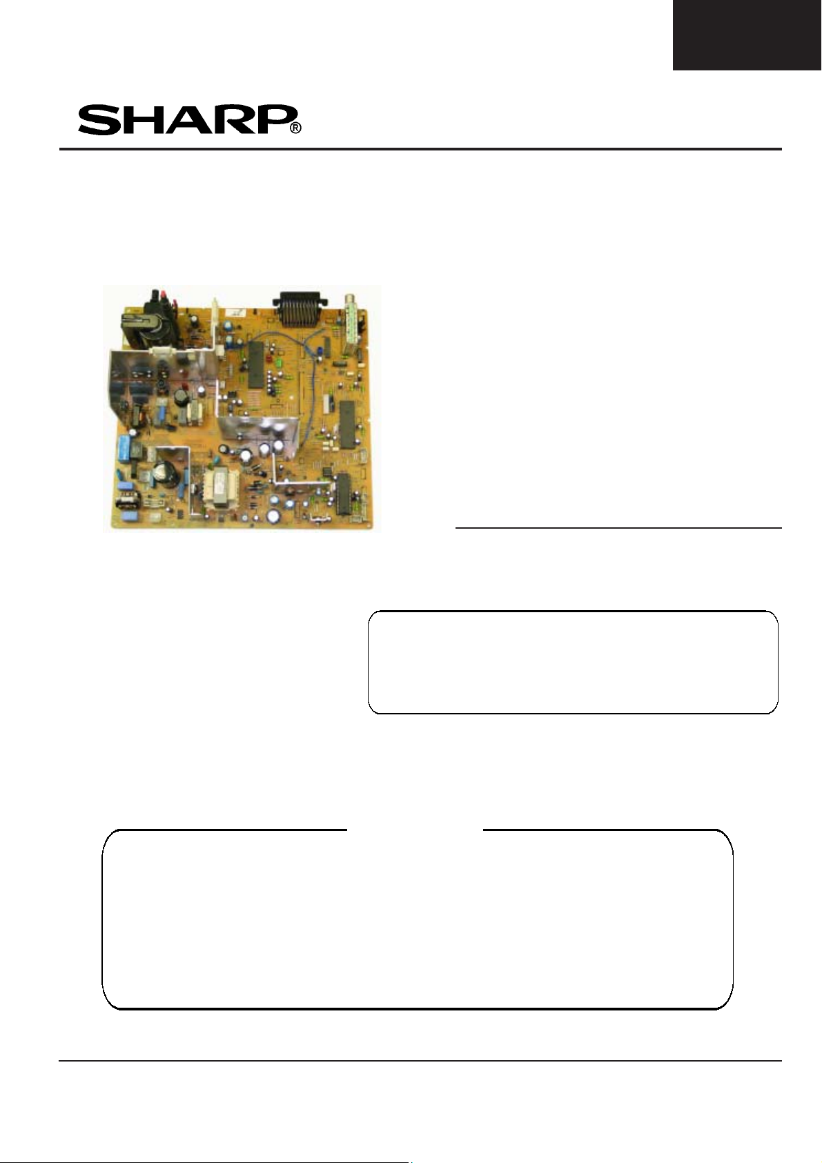
CHASSIS AK-45
In the interests of user safety (required by safety
regulations in some countries) the set should be restored to its original condition and only parts identical to those specified should be used.
CONTENTS
TABLE OF CONTENTS ....................................................................................................... 3
INTRODUCTION .................................................................................................................. 6
CIRCUIT DESCRIPTIONS ................................................................................................... 6
INTEGRATED CIRCUIT DESCRIPTIONS ....................................................................... 10
SERVICE MODE ADJUSTMENTS ...................................................................................... 23
BLOCK DIAGRAM ................................................................................................................ 61
CIRCUIT DIAGRAMS ..................................................................................................... 62
HOW TO UPDATE THE TECHNICAL INFORMATION ...................................................... 73
SHARP CORPORATION
1
This document has been published to
be used for after sales service only.

AK - 45
CHASSIS
SERVICE MANUAL UPDATE LOG SHEET
Technical Report No.
Technical Bulletin No.
Cause / Solution
Part No.
Page No.
Application
Data /Serial No.
Use this page to keep any special servicing information as Technical Report (Bulletin), Technical Information, etc.
If only part number changes are required, just change part number directly the part number in the Parts Listing Section.
If you need more information, please refer to the Technical Report (Bulletin).
2

TABLE OF CONTENTS
1.INTRODUCTION
2.TUNER
.................................................................................................................................................6
3.IF PART (TDA9885/86)
4.VIDEO SWITCH TEA6415
5.MULTI STANDARD SOUND PROCESSOR
6.SOUND OUTPUT STAGE WITH TDA7269A
7.VERTICAL OUTPUT STAGE WITH STV9379FA
8.VIDEO OUTPUT AMPLIFIER TDA6108
9.POWER SUPPLY (SMPS)
10.MICROCONTROLLER SDA55XX
10.1.General Features..........................................................................................................................8
10.2.External Crystal and Programmable Clock Speed ...................................................................8
10.3.Microcontroller Features ............................................................................................................. 8
10.4.Memory..........................................................................................................................................8
10.5.Display Features...........................................................................................................................8
10.6.Acquisition Features....................................................................................................................9
10.7.Ports ..............................................................................................................................................9
11.CLASS AB STEREO HEADPHONE DRIVER TDA1308
12.SAW FILTERS
13.IC DESCRIPTIONS
13.1.LM317T
13.1.1.Description...........................................................................................................................10
13.1.2.Features................................................................................................................................10
13.2.TDA1308T
13.2.1.General Description ............................................................................................................10
13.2.2.Features................................................................................................................................10
13.2.3.Pinning..................................................................................................................................11
13.3.MSP34X0G (MSP3410G)
13.3.1.Description...........................................................................................................................11
13.3.2.Features................................................................................................................................12
13.3.3.Pin connections...................................................................................................................12
13.4.VDP313xY
13.4.1.Introduction..........................................................................................................................13
13.4.2.Features................................................................................................................................14
13.4.3.Pin Connections and short descriptions ..........................................................................14
13.5.TEA6415C
13.5.1.General Description ............................................................................................................15
13.5.2.Features................................................................................................................................15
13.5.3.Pinning..................................................................................................................................16
13.6.STV9379FA
13.6.1.Description...........................................................................................................................16
13.6.2.Features................................................................................................................................16
13.6.3.Pinning..................................................................................................................................16
13.7.TDA7269A
13.7.1.Description...........................................................................................................................17
13.7.2.Features................................................................................................................................17
13.8.LM7800 (LM7805/LM7808)
13.8.1.Description...........................................................................................................................17
13.8.2.Features................................................................................................................................17
13.9.AT24C08
13.9.1.Description...........................................................................................................................17
13.9.2.Features................................................................................................................................17
13.9.3.Pin Configurations ..............................................................................................................18
..............................................................................................................................6
..................................................................................................................6
............................................................................................................7
...........................................................................7
.........................................................................7
.................................................................7
...................................................................................7
............................................................................................................8
...........................................................................................8
.................................................9
................................................................................................................................9
.....................................................................................................................10
....................................................................................................................................10
...............................................................................................................................10
..................................................................................................11
..............................................................................................................................13
..............................................................................................................................15
............................................................................................................................16
..............................................................................................................................17
...............................................................................................17
.................................................................................................................................17
AK - 45
CHASSIS
3

AK - 45
CHASSIS
13.10.SDA5555
13.10.1.General definition .............................................................................................................. 18
13.10.2.Features..............................................................................................................................18
13.11.MC44608
13.11.1.Description.........................................................................................................................19
13.11.2.General Features ...............................................................................................................20
13.11.3.Pin Connections ................................................................................................................20
13.12.TCET1102G
13.12.1.Description.........................................................................................................................21
13.12.2.Applications ....................................................................................................................... 21
13.12.3.Features..............................................................................................................................21
13.13.TDA9885T
13.13.1.General Description ..........................................................................................................21
13.13.2.Features..............................................................................................................................21
13.13.3.Pinning................................................................................................................................22
13.14.PI5V330
13.14.1.General Description .............................................................................................................. 22
14.AK45 CHASSIS PRODUCTION SERVICE MODE ADJUSTMENTS
14.1.SERVICE MENU..........................................................................................................................23
14.2.ADJUST MENU ...........................................................................................................................23
14.3.OPTIONS MENU..........................................................................................................................35
Option 0. Video Processor Crystal Indication .............................................................................35
Option 1. (0x01) Video Processor Decoder Mode Register........................................................35
Option 2. (0x18) Video Processor Blanking Control...................................................................35
Option 3. (0x19) Video Processor Cathode Drive Level .............................................................36
Option 4. ..........................................................................................................................................36
Option 5. CTI Available, Mono AVL...............................................................................................36
Option 6. ..........................................................................................................................................36
Option 7. OPTIONHOTELACTIVE, PLL_VST, PIP Zoom Mode, PIP Position ...........................36
Option 8. IF Frequency...................................................................................................................37
Option 9. Standard Available.........................................................................................................37
Option 10. Scart, Combfilter, Teletext, Language .......................................................................38
Option 11. PLL Tuner Control 1 Byte............................................................................................38
Option 12. PLL Tuner Control 2 Low Byte ...................................................................................38
Option 13. PLL Tuner Control 2 Mid Byte ....................................................................................39
Option 14. PLL Tuner Control 2 High Byte ..................................................................................39
Option 15. PLL Tuner VHF LOW – VHF HIGH Crossover Low Byte ..........................................39
Option 16. PLL Tuner VHF LOW – VHF HIGH Crossover High Byte .........................................39
Option 17. PLL Tuner VHF HIGH – UHF Crossover Low Byte ...................................................39
Option 18. PLL Tuner VHF HIGH – UHF Crossover High Byte...................................................39
Option 19. PIP PLL Tuner Control 1 Byte.....................................................................................40
Option 20. PIP PLL Tuner Control 2 Low Byte ............................................................................40
Option 21. PIP PLL Tuner Control 2 Mid Byte .............................................................................40
Option 22. PIP PLL Tuner Control 2 High Byte............................................................................40
Option 23. PIP PLL Tuner VHF LOW – VHF HIGH Crossover Low Byte ...................................40
Option 24. PIP PLL Tuner VHF LOW – VHF HIGH Crossover High Byte...................................40
Option 25. PIP PLL Tuner VHF HIGH – UHF Crossover Low Byte.............................................41
Option 26. PIP PLL Tuner VHF HIGH – UHF Crossover High Byte............................................ 41
Option 27. Language Available 1 ..................................................................................................41
Option 28. Language Available 2 ..................................................................................................41
Option 29. Language Available 3 and Zoom Mode Available ....................................................41
Option 30. Country .........................................................................................................................42
Option 31. Prescaler MSP FM (AVL=OFF).................................................................................... 42
Option 32. Prescaler MSP NICAM (AVL=OFF) .............................................................................42
Option 33. Prescaler MSP SCART (AVL=OFF) ............................................................................43
Option 34. Prescaler MSP I2S (AVL=OFF)....................................................................................43
Option 35. Not used........................................................................................................................43
Option 36. Not used........................................................................................................................43
Option 37. Reserved for USA ........................................................................................................43
Option 38. TV Teletext Mode Selection, Child Lock, Equalizer Country................................... 43
...............................................................................................................................18
...............................................................................................................................19
.........................................................................................................................21
............................................................................................................................21
.................................................................................................................................22
.........................23
4

AK - 45
CHASSIS
Option 39. Personal Preference Equalizer Band 1 ......................................................................44
Option 40. Personal Preference Equalizer Band 2 ......................................................................44
Option 41. Personal Preference Equalizer Band 3 ......................................................................44
Option 42. Personal Preference Equalizer Band 4 ......................................................................44
Option 43. Personal Preference Equalizer Band 5 ......................................................................44
Option 44. Sound Effect (Standard; Music; Speech; Jazz; Pp) .................................................44
Option 45. Volume Offset Left.......................................................................................................44
Option 46. Volume Offset Right ....................................................................................................44
Option 47. Volume Offset Center ..................................................................................................45
Option 48. Volume Offset Rear......................................................................................................45
Option 49. Surround Delay ............................................................................................................45
Option 50. FM Prescaler.................................................................................................................45
Option 51. NICAM Prescaler .......................................................................................................... 45
Option 52. Scart Input Prescaler...................................................................................................45
Option 53. I2S Prescaler ................................................................................................................45
Option 54. Scart Output Prescaler................................................................................................45
Option 55. Speaker Setup .............................................................................................................46
Option 56. Audio Options Available Or Not .................................................................................46
Option 57. Stereo Threshold .........................................................................................................46
Option 58. MSP Audio Flags..........................................................................................................47
Option 59. NICAM Threshold......................................................................................................... 47
Option 60. Power Delay Time ........................................................................................................47
14.4.OPTION TABLE RECOMMENDED VALUES.............................................................................50
14.5.SCREEN ADJUSTMENT (FBT SCREEN) .................................................................................. 52
14.6.GEOMETRY ADJUSTMENT ....................................................................................................... 53
4:3 FORMATS..................................................................................................................................53
16:9 FORMATS................................................................................................................................54
15.BLOCK DIAGRAM
16.CIRCUIT DIAGRAMS
17. HOW TO UPDATE THE TECHNICAL INFORMATION
17.1. HOW TO UPDATE THE TECHNICAL INFORMATION APPEARED ON THIS SERVICE
MANUAL (AND RELATIVES) ....................................................................................................73
17.2. NVM / EEPROM RECORDER ....................................................................................................73
17.3. CHASSIS LABEL INFORMATION............................................................................................. 73
17.4. CODE BAR LABEL INFORMATION..........................................................................................74
......................................................................................................................61
.................................................................................................................62
………………………………… 73
5

AK - 45
CHASSIS
1.INTRODUCTION
11AK45 is a 50Hz colour television capable of driving 24” + CRT sizes (beginning from 24” 16:9 up to
33”).
The chassis is capable of operation in PAL, SECAM, NTSC (playback) colour standards and multiple
transmission standards as B/G, D/K, I/I’, and L/L´.
Sound system output is supplying 2x10W (10%THD) for left and right outputs of 8ohm speakers.
TV supports FASTTEXT. It is possible to decode transmissions including high graphical data.
The chassis is equipped with three full EuroScarts; only one of them supports RGB input, one
headphone output, one FAV input, one SVHS input (via SCART)
2.TUNER
The hardware and software of the TV is suitable for tuners, supplied by different companies, which are
selected from the Service Menu. These tuners can be combined VHF, UHF tuners suitable for CCIR
systems B/G, H, L, L´, I/I´, and D/K. The tuning is available through the digitally controlled I
2
C bus
(PLL). Below you will find info on one of the Tuners in use.
General description of UV1316:
The UV1316 tuner belongs to the UV 1300 family of tuners, which are designed to meet a wide range
of applications. It is a combined VHF, UHF tuner suitable for CCIR systems B/G, H, L, L’, I and I’. The
low IF output impedance has been designed for direct drive of a wide variety of SAW filters with
sufficient suppression of triple transient.
Features of UV1316:
1. Member of the UV1300 family small sized UHF/VHF tuners
2. Systems CCIR: B/G, H, L, L’, I and I’; OIRT: D/K
3. Digitally controlled (PLL) tuning via I
2
C-bus
4. Off-air channels, S-cable channels and Hyperband
5. World standardized mechanical dimensions and world standard pinning
6. Compact size
7. Complies to “CENELEC EN55020” and “EN55013”
Pinning:
1. Gain control voltage (AGC) : 4.0V, Max: 4.5V
2. Tuning voltage
3. I²C-bus address select : Max: 5.5V
4. I²C-bus serial clock : Min:-0.3V, Max: 5.5V
5. I²C-bus serial data : Min:-0.3V, Max: 5.5V
6. Not connected
7. PLL supply voltage : 5.0V, Min: 4.75V, Max: 5.5V
8. ADC input
9. Tuner supply voltage : 33V, Min: 30V, Max: 35V
10. Symmetrical IF output 1
11. Symmetrical IF output 2
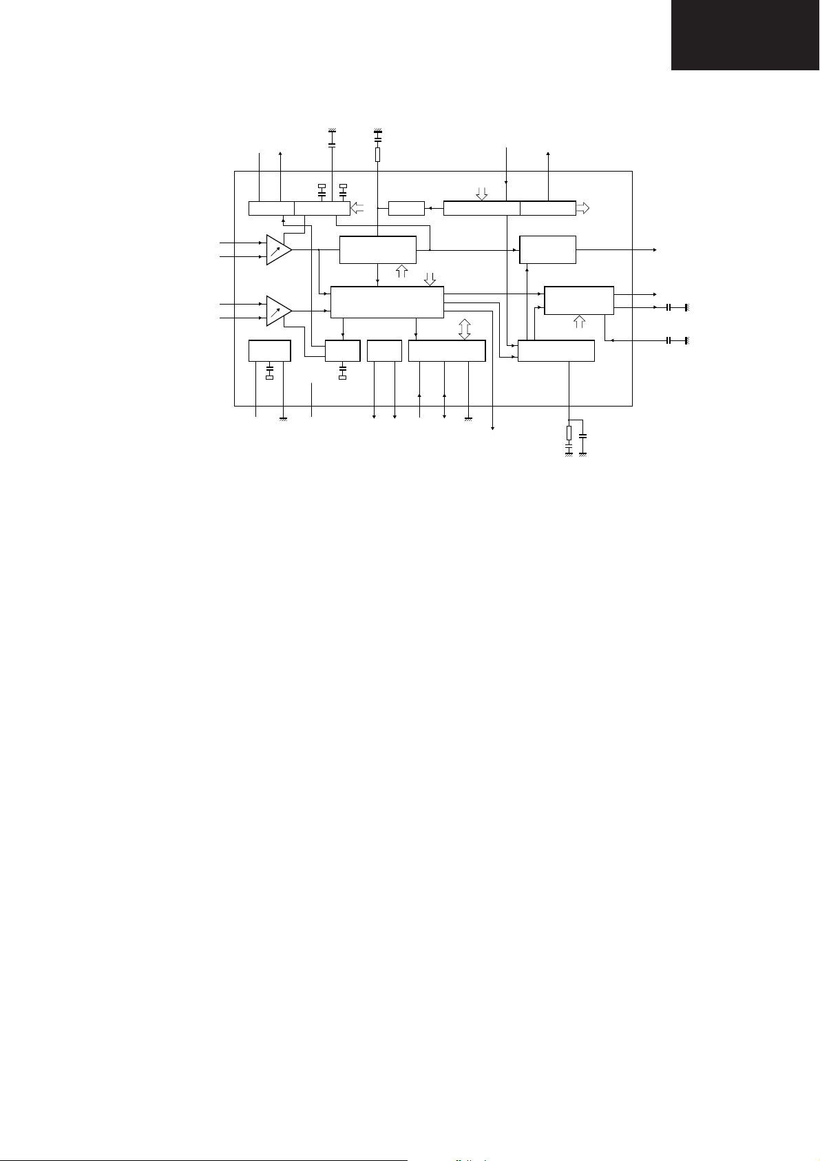
3.IF PART (TDA9885/86)
The TDA9885 is an alignment-free single standard (without positive modulation) vision and sound IF signal
PLL.
The TDA9886 is an alignment-free multistandard (PAL, SECAM and NTSC) vision and sound IF signal PLL
Both devices can be used for TV, VTR, PC and set-top box applications.
The following figure shows the simplified block diagram of the integrated circuit.
The integrated circuit comprises the following functional blocks:
VIF amplifier, Tuner and VIF-AGC, VIF-AGC detector, Frequency Phase-Locked Loop (FPLL) detector, VCO
and divider, Digital acquisition help and AFC, Video demodulator and amplifier, Sound carrier trap, SIF
amplifier, SIF-AGC detector, Single reference QSS mixer, AM demodulator, FM demodulator and acquisition
help, Audio amplifier and mute time constant, I
voltage stabilizer.
2
C-bus transceivers and MAD (module address), Internal
6
u
C
VAGC(pos)
(1)
TAGC
TOP
14 (15)
C
AGC(neg)
TUNER AGC
VIF2
2 (31)
1 (30)
VIF1
SIF2
24 (27)
23 (26)
SIF1
SUPPLY SIF-AGC
V
P
(1) Not connected for TDA9885.
Pin numbers for TDA9885HN and TDA9886HN in parenthesis.
VAGC
C
VIF-AGC
BL
SINGLE REFERENCE QSS MIXER
INTERCARRIER MIXER
AND AM DEMODULATOR
C
AGC
(6, 12, 13, 14, 17,
19, 25, 28, 29, 32)
13
n.c.AGND
VIF-PLL
ll pagewidth
external reference signal
VIF-PLL
filter
VPLL
19 (21)9 (8) 16 (17) 15 (16) 21 (23)
RC VCO
MAD
OUTPUT
I2C-BUS TRANSCEIVER
PORTS
11 (10)
22 (24)3 (1)
OP1 OP2 FMPLL
or 4 MHz crystal
REF AFC
DIGITAL VCO CONTROL AFC DETECTOR
SOUND CARRIER
TRAPS
FM-PLL DEMODULATOR
12 (11)18 (20)20 (22)
SIOMADSDASCL
4.5 to 6.5 MHz
AUDIO PROCESSING
AND SWITCHES
NARROW-BAND
TDA9885
TDA9886
7 (5)
DGND
sound intercarrier output
and MAD select
AK - 45
CHASSIS
(18) 17
CVBS
video output: 2 V (p-p)
[1.1 V (p-p) without trap]
AUD
(7) 8
(3) 5
(4) 6
4 (2)10 (9)
FM-PLL
filter
MHC108
DEEM
AFD
audio output
de-emphasis
network
C
AF
4.VIDEO SWITCH TEA6415
In case of three or more external sources are used, the video switch IC TEA6415 is used. The main
function of this device is to switch 8 video-input sources on the 6 outputs.
Each output can be switched on only one of each input. On each input an alignment of the lowest level
of the signal is made (bottom of sync. top for CVBS or black level for RGB signals).
Each nominal gain between any input and output is 6.5dB.For D2MAC or Chroma signal the alignment
is switched off by forcing, with an external resistor bridge, 5VDC on the input. Each input can be used
as a normal input or as a MAC or Chroma input (with external Resistor Bridge). All the switching
possibilities are changed through the BUS. Driving 75ohm load needs an external resistor. It is possible
to have the same input connected to several outputs.
5.MULTI STANDARD SOUND PROCESSOR
The MSP 34x10G family of single-chip Multi-standard Sound Processors covers the sound processing
of all analog TV-Standards worldwide, as well as the NICAM digital sound standards. The full TV sound
processing, starting with analog sound IF signal-in, down to processed analog AF-out, is performed on
a single chip.
The DBX noise reduction, or alternatively, MICRONAS Noise Reduction (MNR) is performed alignment
free.
6.SOUND OUTPUT STAGE WITH TDA7269A
The TDA7269A is class AB dual Audio power amplifier assembled in the Multi-watt package, specially
designed for high quality sound application as Hi-Fi music centers and stereo TV sets.
7.VERTICAL OUTPUT STAGE WITH STV9379FA
The IC STV9379FA is the vertical deflection booster circuit. Two supply voltages, +14V and –14V are
needed to scan the inputs VERT+ and VERT-, respectively. And a third supply voltage, +60V for the
flyback limiting is needed. The vertical deflection coil is connected in series between the output and
feedback to the input.
8.VIDEO OUTPUT AMPLIFIER TDA6108
The TDA6108Q includes three video output amplifiers is intended to drive the three cathodes of a
colour picture tube.
7

AK - 45
CHASSIS
9.POWER SUPPLY (SMPS)
The DC voltages required at various parts of the chassis are provided by an SMPS transformer
controlled by the IC MC44608, which is designed for driving, controlling and protecting switching
transistor of SMPS. The transformer generates 145V for Horizontal output stage, +/-14V for audio
amplifier, 5V and 3.3V stand by voltage and 8V, 12V and 5V supplies for other different parts of the chassis.
An optocoupler is used to control the regulation of line voltage and stand-by power consumption. There
is a regulation circuit in secondary side. This circuit produces a control voltage according to the
changes in 145V DC voltage, via an optocoupler (TCET1102G) to pin3 of the IC.
During the switch on period of the transistor, energy is stored in the transformer. During the switch off
period energy is fed to the load via secondary winding. By varying switch-on time of the power
transistor, it controls each portion of energy transferred to the secondary side such that the output
voltage level remains nearly independent of load variations.
10.MICROCONTROLLER SDA55XX
10.1.General Features
• Feature selection via special function register
• Simultaneous reception of TTX, VPS, PDC, and WSS (line 23)
• Supply Voltage 2.5 and 3.3 V
• ROM version package PSDIP52-2, PMQFP64-1
• Romless version package PMQFP100-2, PLCC84-2
10.2.External Crystal and Programmable Clock Speed
• Single external 6MHz crystal, all necessary clocks are generated internally
• CPU clock speed selectable via special function registers.
• Normal Mode 33.33 MHz CPU clock, Power Save mode 8.33 MHz
10.3.Microcontroller Features
• 8bit 8051 instruction set compatible CPU.
• 33.33-MHz internal clock (max.)
• 0.360 ms (min.) instruction cycle
• Two 16-bit timers
• Watchdog timer
• Capture compare timer for infrared remote control decoding
• Pulse width modulation unit (2 channels 14 bit, 6 channels 8 bit)
• ADC (4 channels, 8 bit)
• UART (rxd, txd)
10.4.Memory
• Non-multiplexed 8-bit data and 16 … 20-bit address bus (ROMless Version)
• Memory banking up to 1Mbyte (Romless version)
• Up to 128 Kilobyte on Chip Program ROM
• Eight 16-bit data pointer registers (DPTR)
• 256-bytes on-chip Processor Internal RAM (IRAM)
• 128bytes extended stack memory.
• Display RAM and TXT/VPS/PDC/WSS-Acquisition-Buffer directly accessible via MOVX
• UP to 16KByte on Chip Extended RAM (XRAM) consisting of;
- 1 Kilobyte on-chip ACQ-buffer-RAM (access via MOVX)
- 1 Kilobyte on-chip extended-RAM (XRAM, access via MOVX) for user software
- 3 Kilobyte Display Memory
10.5.Display Features
• ROM Character Set Supports all East and West European Languages in single device
• Mosaic Graphic Character Set
• Parallel Display Attributes
• Single/Double Width/Height of Characters
• Variable Flash Rate
• Programmable Screen Size (25 Rows x 33...64 Columns)
• Flexible Character Matrixes (HxV) 12 x 9...16
• Up to 256 Dynamical Redefinable Characters in standard mode; 1024 Dynamical Redefinable
Characters in Enhanced Mode
• CLUT with up to 4096 colour combinations
8

AK - 45
CHASSIS
• Up to 16 Colours per DRCS Character
• One out of Eight Colours for Foreground and Background Colours for 1-bit DRCS and ROM
Characters
• Shadowing
• Contrast Reduction
• Pixel by Pixel Shiftable Cursor With up to 4 Different Colours
• Support of Progressive Scan and 100 Hz.
• 3 X 4Bits RGB-DACs On-Chip
• Free Programmable Pixel Clock from 10 MHz to 32MHz
• Pixel Clock Independent from CPU Clock
• Multinorm H/V-Display Synchronization in Master or Slave Mode
10.6.Acquisition Features
• Multi-standard Digital Data Slicer
• Parallel Multi-norm Slicing (TTX, VPS, WSS, CC, G+)
• Four Different Framing Codes Available
• Data Caption only limited by available Memory
• Programmable VBI-buffer
• Full Channel Data Slicing Supported
• Fully Digital Signal Processing
• Noise Measurement and Controlled Noise Compensation
• Attenuation Measurement and Compensation
• Group Delay Measurement and Compensation
• Exact Decoding of Echo Disturbed Signals
10.7.Ports
• One 8-bit I/O-port with open drain output and optional I
2
C Bus emulation support (Port0)
• Two 8-bit multifunction I/O-ports (Port1, Port3)
• One 4-bit port working as digital or analogue inputs for the ADC (Port2)
• One 2-bit I/O port with secondary function (P4.2, 4.3, 4.7)
• One 4-bit I/O-port with secondary function (P4.0, 4.1, 4.4) (Not available in P-SDIP 52)
11.CLASS AB STEREO HEADPHONE DRIVER TDA1308
The TDA1308 is an integrated class AB stereo headphone driver contained in a DIP8 plastic package.
The device is fabricated in a 1 mm CMOS process and has been primarily developed for portable digital
audio applications.
12.SAW FILTERS
K3953M:
Standard
B/G, D/K, I, L/L’
Features
TV IF filter with Nyquist slopes at 33,90 MHz and 38,90 MHz
Constant group delay
Suitable for CENELEC EN 55020
Terminals
Tinned CuFe alloy
Pin configuration
1 Input
2 Input - ground
3 Chip carrier - ground
4 Output
5 Output
K3958M:
Standard
B/G, D/K, I, L/L’
Features
TV IF filter with Nyquist slopes at 33.90 MHz and 38.90 MHz
Constant group delay
Terminal and Pin configuration are the same with
K3953M
9

AK - 45
CHASSIS
K9356M:
Standard
B/G, D/K, I, L
Features
TV IF audio filter with pass band for sound carriers at 32,40 MHz (D/K, L), 32,90 MHz (I) and 33,40 MHz
(B/G)
Terminal and Pin configuration are the same with
K3953M
K9656M:
Standard
B/G, D/K, I, L/L’
Features
TV IF audio filter with two channels
Channel 1 (L’) with one pass band for sound carriers at 40,40 MHz (L’) and 39,75 MHz (L’- NICAM)
Channel 2 (B/G, D/K, L, I) with one pass band for sound carriers between 32,35 MHz and 33,40 MHz
Terminal and Pin configuration are the same with
K3953M
13.IC DESCRIPTIONS
LM317T TDA1308T
MSP3410G VDP3130Y
TEA6415 STV9379FA
TDA7269A LM7805/LM7808
24C08 SDA55XX
MC44608 TCET1102G
TDA9885T
13.1.LM317T
13.1.1.Description
The LM317T is an adjustable 3 terminal positive voltage regulator capable of supplying in excess of 1.5
amps over an output range of 1.25 to 37 volts. This voltage regulator is exceptionally easy to use and
requires only two external resistors to set the output voltage. Further, it employs internal current limiting,
thermal shutdown and safe area compensation, making it essentially blow–out proof. The LM317
serves a wide variety of applications including local, on card regulation. This device can also be used to
make a programmable output regulator, or by connecting a fixed resistor between the adjustment and
output, the LM317 can be used as a precision current regulator.
13.1.2.Features
• Output Current in Excess of 1.5 A
• Output Adjustable between 1.2 V and 37 V
• Internal Thermal Overload Protection
• Internal Short Circuit Current Limiting Constant with Temperature
• Output Transistor Safe–Area Compensation
• Floating Operation for High Voltage Applications
• Available in Surface Mount D
2
PAK, and Standard 3–Lead Transistor Package
• Eliminates Stocking many Fixed Voltages
13.2.TDA1308T
13.2.1.General Description
The TDA1308 is an integrated class AB stereo headphone driver contained in an SO8 or a DIP8 plastic
package. The device is fabricated in a 1 mm CMOS process and has been primarily developed for
portable digital audio applications. It gets its input from two analog audio outputs (DACA_L and
DACA_R) of MSP 34x0G. The gain of the output is adjustable by the feedback resistor between the
inputs and outputs.
13.2.2.Features
Wide temperature range
•
No switch ON/OFF clicks
•
Excellent power supply ripple rejection
•
10
Low power consumption
•
Short-circuit resistant
•
High performance
•
high signal-to-noise ratio
•
High slew rate
•
Low distortion
•
Large output voltage swing.
•
13.2.3.Pinning
SYMBOL PIN DESCRIPTION
OUTA 1 Output A
INA(neg) 2 Inverting input A
INA(pos) 3 Non-inverting input A
VSS 4 Negative supply
INB(pos) 5 Non-inverting input B
INB(neg) 6 Inverting input B
OUTB 7 Output B
VDD 8 Positive supply
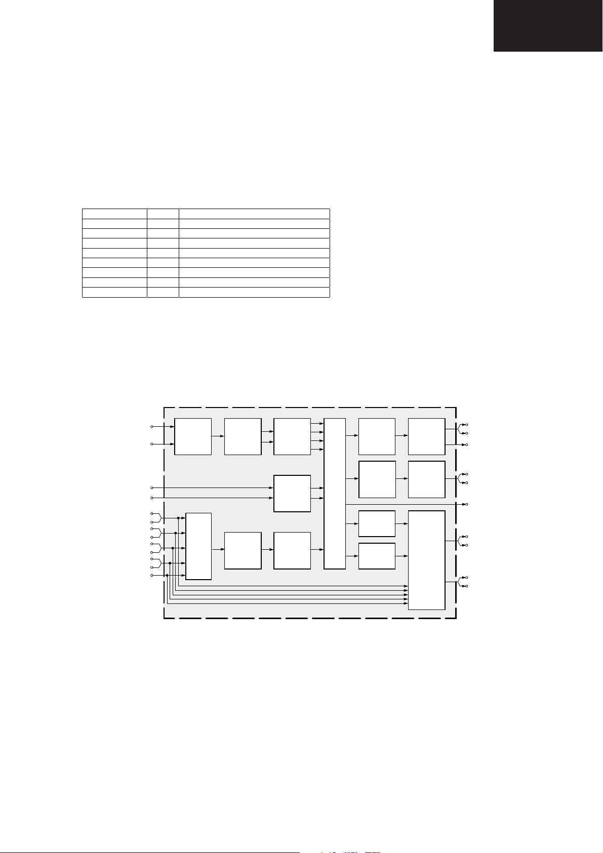
13.3.MSP34X0G (MSP3410G)
AK - 45
CHASSIS
13.3.1.Description
The MSP 34x0G family of single-chip Multi standard Sound Processors covers the sound processing of
all analog TV-Standards worldwide, as well as the NICAM digital sound standards. The full TV sound
processing, starting with analog sound IF signal-in, down to processed analog AF-out, is performed on
a single chip. Figure shows a simplified functional block diagram of the MSP 34x0G.
Sound IF1
Sound IF2
I2S1
I2S2
SCART1
SCART2
SCART3
SCART4
MONO
ADC
SCART
DSP
Input
Select
De-
modulator
ADC
Pre-
processing
Prescale
Prescale
Source Select
Loud-
speaker
Sound
Processing
Headphone
Sound
Processing
DAC
DAC
DAC
DAC
SCART
Output
Select
Loudspeaker
Subwoofer
Headphone
I2S
SCART1
SCART2
This new generation of TV sound processing ICs now includes versions for processing the multi
channel television sound (MTS) signal conforming to the standard recommended by the Broadcast
Television Systems Committee (BTSC). The DBX noise reduction, or alternatively, MICRONAS Noise
Reduction (MNR) is performed alignment free. Other processed standards are the Japanese FM-FM
multiplex standard (EIA-J) and the FM Stereo Radio standard. Current ICs have to perform adjustment
procedures in order to achieve good stereo separation for BTSC and EIA-J. The MSP 34x0G has
optimum stereo performance without any adjustments.
All MSP 34x0G versions are pin and software downward compatible to the MSP34x0D. The
MSP34x0G further simplifies controlling software. Standard selection requires a single I
2
C transmission
only.
The MSP 34x0G has built-in automatic functions: The IC is able to detect the actual sound standard
automatically (Automatic Standard Detection). Furthermore, pilot levels and identification signals can be
evaluated internally with subsequent switching between mono/stereo/bilingual; no I
2
C interaction is
necessary (Automatic Sound Selection).
11

AK - 45
CHASSIS
13.3.2.Features
2
Standard Selection with single I
C transmission
Automatic Standard Detection of terrestrial TV standards
Automatic Sound Selection (mono/stereo/bilingual), new registers MODUS, STATUS
Two selectable sound IF (SIF) inputs
Automatic Carrier Mute function
Interrupt output programmable (indicating status change)
Loudspeaker / Headphone channel with volume, balance, bass, treble, loudness
AVC: Automatic Volume Correction
Subwoofer output with programmable low-pass and complementary high-pass filter
5-band graphic equalizer for loudspeaker channel
Spatial effect for loudspeaker channel
Four Stereo SCART (line) inputs, one Mono input; two Stereo SCART outputs
Complete SCART in/out switching matrix
2
Two I
S inputs; one I2S output
Dolby Pro Logic with DPL 351xA coprocessor
All analog FM-Stereo A2 and satellite standards; AM-SECAM L standard
Simultaneous demodulation of (very) high-deviation FM-Mono and NICAM
Adaptive deemphasis for satellite (Wegener-Panda, acc. to ASTRA specification)
ASTRA Digital Radio (ADR) together with DRP 3510A
All NICAM standards
Korean FM-Stereo A2 standard
13.3.3.Pin connections
NC = not connected; leave vacant
LV = if not used, leave vacant
X = obligatory; connect as described in circuit diagram
DVSS: if not used, connect to DVSS
AHVSS: connect to AHVSS
Pin No.
PLCC
68-pin
1 16 14 9 8 ADR_WS OUT LV ADR word strobe
2 - - - - NC LV Not connected
3 15 13 8 7 ADR_DA OUT LV ADR Data Output
4 14 12 7 6 I2S_DA_IN1 IN LV I2S1 data input
5 13 11 6 5 I2S_DA_OUT OUT LV I2S data output
6 12 10 5 4 I2S_WS IN/OUT LV I2S word strobe
7 11 9 4 3 I2S_CL IN/OUT LV I2S clock
8 10 8 3 2 I2C_DA IN/OUT X I2C data
9 9 7 2 1 I2C_CL IN/OUT X I2C data
10 8 - 1 64 NC LV Not connected
11 7 6 80 63 STANDBYQ IN X Stand-by (low-active)
12 6 5 79 62 ADR_SEL IN X I2C bus address select
13 5 4 78 61 D_CTR_I/O_0 IN/OUT LV D_CTR_I/O_0
14 4 3 77 60 D_CTR_I/O_1 IN/OUT LV D_CTR_I/O_1
15 3 - 76 59 NC LV Not connected
16 2 - 75 58 NC LV Not connected
17 - - - - NC LV Not connected
18 1 2 74 57 AUD_CL_OUT OUT LV
19 64 1 73 56 TP LV Test pin
20 63 52 72 55 XTAL_OUT OUT X Crystal oscillator
21 62 51 71 54 XTAL_IN IN X Crystal oscillator
22 61 50 70 53 TESTEN IN X Test pin
23 60 49 69 52 ANA_IN2+ IN
24 59 48 68 51 ANA_IN- IN
25 58 47 67 50 ANA_IN1+ IN LV IF input 2
26 57 46 66 49 AVSUP X Analog power supply 5v
- - - 65 - AVSUP X Analog power supply 5v
PSDIP
64-pin
PSDIP
52-pin
PQFP
80-pin
PLQFP
64-pin
Pin Name
Type
Connection
(if not used)
AVSS via 56
pF/LV
AVSS via 56
pF/LV
Short Description
Audio clock output
(18.432 MHz)
IF Input 2 (can be left
vacant, only if IF input 1 is
also not in use)
IF common (can be left
vacant, only if IF input 1 is
also not in use)
12

AK - 45
CHASSIS
- - - 64 - NC LV Not connected
- - - 63 - NC LV Not connected
27 56 45 62 48 AVSS X Analog ground
- - - 61 - AVSS X Analog ground
28 55 44 60 47 MONO_IN IN LV Mono input
- - - 59 - NC LV Not connected
29 54 43 58 46 VREFTOP X
30 53 42 57 45 SC1_IN_R IN LV SCART 1 input, right
31 52 41 56 44 SC1_IN_L IN LV SCART 1 input, left
32 51 - 55 43 ASG1 AHVSS Analog Shield Ground 1
33 50 40 54 42 SC2_IN_R IN LV SCART 2 input, right
34 49 39 53 41 SC2_IN_L IN LV SCART 2 input, left
35 48 - 52 40 ASG2 AHVSS Analog Shield Ground 2
36 47 38 51 39 SC3_IN_R IN LV SCART 3 input, right
37 46 37 50 38 SC3_IN_L IN LV SCART 3 input, left
38 45 - 49 37 ASG4 AHVSS Analog Shield Ground 4
39 44 - 48 36 SC4_IN_R IN LV SCART 4 input, right
40 43 - 47 35 SC4_IN_L IN LV SCART 4 input, left
41 - - 46 - NC LV or AHVSS Not connected
42 42 36 45 34 AGNDC X Analog reference voltage
43 41 35 44 33 AHVSS X Analog ground
- - - 43 - AHVSS X Analog ground
- - - 42 - NC LV Not connected
- - - 41 - NC LV Not connected
44 40 34 40 32 CAPL_M X Volume capacitor MAIN
45 39 33 39 31 AHVSUP X Analog power supply 8V
46 38 32 38 30 CAPL_A X Volume capacitor AUX
47 37 31 37 29 SC1_OUT_L OUT LV SCART output 1, left
48 36 30 36 28 SC1_OUT_R OUT LV SCART output 1, right
49 35 29 35 27 VREF1 X Reference ground 1
50 34 28 34 26 SC2_OUT_L OUT LV SCART output 2, left
51 33 27 33 25 SC2_OUT_R OUT LV SCART output 2, right
52 - - 32 - NC LV Not connected
53 32 - 31 24 NC LV Not connected
54 31 26 30 23 DACM_SUB OUT LV Subwoofer output
55 30 - 29 22 NC LV Not connected
56 29 25 28 21 DACM_L OUT LV Loudspeaker out, left
57 28 24 27 20 DACM_R OUT LV Loudspeaker out, right
58 27 23 26 19 VREF2 X Reference ground 2
59 26 22 25 18 DACA_L OUT LV Headphone out, left
60 25 21 24 17 DACA_R OUT LV Headphone out, right
- - - 23 - NC LV Not connected
- - - 22 - NC LV Not connected
61 24 20 21 16 RESETQ IN X Power-on-reset
62 23 - 20 15 NC LV Not connected
63 22 - 19 14 NC LV Not connected
64 21 19 18 13 NC LV Not connected
65 20 18 17 12 I2S_DA_IN2 IN LV I2S2-data input
66 19 17 16 11 DVSS X Digital ground
- - - 15 - DVSS X Digital ground
- - - 14 - DVSS X Digital ground
67 18 16 13 10 DVSUP X Digital power supply 5V
- - - 12 - DVSUP X Digital power supply 5V
- - - 11 - DVSUP X Digital power supply 5V
68 17 15 10 9 ADR_CL OUT LV ADR clock
Reference voltage IF A/D
converter
13.4.VDP313xY
13.4.1.Introduction
The VDP 313xY is a video IC family of high-quality single-chip video processors. Modular design and a
sub-micron technology allow the economic integration of features in all classes of TV sets. The VDP
RCB
313xY family is based on the VDP 31xxB including YC
inputs for DVD component signals.
The VDP 313xY includes complete video, display and deflection processing. All processing is done
digitally, the video front-end and video backend are interfacing to the analog world. Most functions of
the VDP can be controlled by software via I
2
C-Bus interface
13

AK - 45
CHASSIS
13.4.2.Features
Video Decoding and Processing
R C B
– four CVBS, one S-VHS input, one YC
component input
– integrated high-quality A/D converters and associated clamp and AGC circuits
– adaptive 2H comb filter Y/C separator
– multistandard colour decoder PAL/NTSC/SECAM including all substandards
– multistandard sync decoder
– automatic standard recognition
– black-line detector
– linear horizontal scaling (0.25...4), as well as non-linear horizontal scaling “Panoramavision”
– black-level expander
– dynamic peaking
– soft limiter (gamma correction)
– colour transient improvement
RGB Processing and Deflection
– programmable RGB matrix
– two analog RGB / Fastblank inputs
– half-contrast switch
– picture frame generator
– scan velocity modulation output
– high-performance H/V deflection
– separate ADC for tube measurements
– EHT compensation
– angle and bow correction
– one 20.25 MHz crystal, few external components
2
–I
C-Bus Interface
– 64-pin PSDIP package
13.4.3.Pin Connections and short descriptions
NC = not connected LV = if not used, leave vacant
X = obligatory; connect as described in circuit diagram IN = Input
OUT = Output SUPPLY = Supply Pin
Pin no
PSDIP 64-pin
1 TEST IN GNDD Test Input
2 RESQ IN X Reset Input
3 SCL IN/OUT X I2C Bus Clock
4 SDA IN/OUT X I2C Bus Data
5 GNDD SUPPLY X Digital Ground
6 HCS IN LV Half Contrast Switch Input
7 FSY OUT LV Front Sync Output
8 CSY OUT LV Composite Sync Output
9 VS OUT LV Vertical Sync Output
10 INTLC OUT LV Interface Control Output
11 VPROT IN GNDAB Vertical Protection Input
12 SAFETY IN GNDAB Safety Input
13 HFLB IN HOUT Horizontal Flyback Input
14 GNDD SUPPLY X Digital Ground
15 VSUPD SUPPLY X Digital Supply Voltage (3.3V)
16 GNDD SUPPLY X Digital Ground
17 VSUPD SUPPLY LV Digital Supply Voltage (3.3V)
18 P0 IN/OUT LV Port 1, Bit 0
19 P1 IN/OUT LV Port 1, Bit 1
20 P2 IN/OUT GNDD Port 1, Bit 2
21 P3 IN/OUT GNDD Port 1, Bit 3
22 P4 IN/OUT GNDD Port 1, Bit 4
23 P5 IN/OUT GNDD Port 1, Bit 5
24 P6 IN/OUT GNDD Port 1, Bit 6
Pin name Type Connection
(if not used)
Short description
(=VS Bit of MSY for TPU)
14

25 GNDD SUPPLY X Digital Ground
26 RSW2 OUT GNDAB Range Switch 2 for Measurement ADC
27 RSW1 OUT GNDAB Range Switch 1 for Measurement ADC
28 SENSE IN GNDAB Sense ADC Input
29 GNDM SUPPLY X Ground, MADC Input
30 VERTQ OUT LV Inverted Vertical Sawtooth Output
31 VERT OUT LV Vertical Sawtooth Output
32 E/w OUT LV Vertical Parabola Output
33 XREF IN X Reference Input for RGB DACs
34 SVMOUT OUT VSUPAB Analog Scan Velocity Modulation Output
35 GNDAB SUPPLY X Analog Ground Backend
36 VSUPAB SUPPLY X Analog Supply Voltage (5.0V) Backend
37 ROUT OUT VSUPAB Analog Red Output
38 GOUT OUT VSUPAB Analog Green Output
39 BOUT OUT VSUPAB Analog Blue Output
40 VRD IN X DAC Reference
41 RIN IN GNDAB Analog Red Input
42 GIN IN GNDAB Analog Green Input
43 BIN IN GNDAB Analog Blue Input
44 FBLIN IN GNDAB Fast Blank Input
45 RIN2 IN GNDAB Analog Red Input2
46 GIN2 IN GNDAB Analog Green Input2
47 BIN2 IN GNDAB Analog Blue Input2
48 FBLIN2 IN GNDAB Fast Blank Input2
49 CLK20 OUT LV 20.25 MHz System Clock Output
50 HOUT OUT X Horizontal Drive Output
51 XTAL 1 IN X Analog Crystal Input
52 XTAL 2 OUT X Analog Crystal Output
53 CIN 2/CRIN LV Analog Chroma 2/Component CR Input
54 CBIN IN LV Component CB Input
55 GNDAF SUPPLY X Analog Ground Front-end
56 SGND IN GNDAF Signal Ground for Analog Input
57 VRT IN X Reference Voltage Top, Video ADC
58 VSUPAF SUPPLY X Analog Supply Voltage (5.0V) Front-end
59 VOUT OUT LV Analog Video Output
60 CIN1 IN VRT Analog Chroma 1 Input
61 VIN1 IN VRT Analog Video 1 Input
62 VIN2 IN VRT Analog Video 2 Input
63 VIN3 IN VRT Analog Video 3 Input
64 VIN4 IN VRT Analog Video 4 Input
13.5.TEA6415C
AK - 45
CHASSIS
13.5.1.General Description
The main function of the IC is to switch 8 video input sources on 6 outputs. Each output can be
switched on only one of each input. On each input an alignment of the lowest level of the signal is made
(bottom of synch. top for CVBS or black level for RGB signals). Each nominal gain between any input
and output is 6.5dB. For D2MAC or Chroma signal the alignment is switched off by forcing, with an
DC
external resistor bridge, 5 V
on the input. Each input can be used as a normal input or as a MAC or
Chroma input (with external resistor bridge). All the switching possibilities are changed through the
BUS. Driving 75 load needs an external transistor. It is possible to have the same input connected to
several outputs. The starting configuration upon power on (power supply: 0 to 10V) is undetermined. In
this case, 6 words of 16 bits are necessary to determine one configuration. In other case, 1 word of 16
bits is necessary to determine one configuration.
13.5.2.Features
• 20MHz Bandwidth
• Cascadable with another TEA6415C (Internal address can be changed by pin 7 voltage)
• 8 Inputs (CVBS, RGB, MAC, CHROMA,...)
• 6 Outputs
• Possibility of MAC or chroma signal for each input by switching-off the clamp with an external resistor
bridge
• Bus controlled
15

AK - 45
CHASSIS
• 6.5dB gain between any input and output
• 55dB crosstalk at 5mHz
• Fully ESD protected
13.5.3.Pinning
1. Input: Max: 2Vpp, Input Current: 1mA, Max: 3mA
2. Data : Low level: -0.3V Max: 1.5V,
High level: 3.0V Max: Vcc+0.5V
3. Input: Max: 2Vpp, Input Current: 1mA, Max: 3mA
4. Clock: Low level : -0.3V Max: 1.5V,
High level: 3.0V Max: Vcc+0.5V
5. Input: Max : 2Vpp, Input Current: 1mA, Max: 3mA
6. Input: Max: 2Vpp, Input Current: 1mA, Max: 3mA
7. Prog
8. Input: Max : 2Vpp, Input Current: 1mA, Max: 3mA
9. Vcc: 12V
10. Input: Max : 2Vpp, Input Current: 1mA, Max: 3mA
11. Input: Max : 2Vpp, Input Current: 1mA, Max: 3mA
12. Ground
13. Output: 5.5Vpp, Min: 4.5Vpp
14. Output: 5.5Vpp, Min: 4.5Vpp
15. Output: 5.5Vpp, Min: 4.5Vpp
16. Output: 5.5Vpp, Min: 4.5Vpp
17. Output: 5.5Vpp, Min: 4.5Vpp
18. Output: 5.5Vpp, Min: 4.5Vpp
19. Ground
20. Input: Max: 2Vpp, Input Current: 1mA, Max: 3mA
13.6.STV9379FA
13.6.1.Description
Designed for monitors and high performance TVs, the STV9379FA vertical deflection booster can
handle flyback voltage up to 90V. Further to this, it is possible to have a flyback voltage, which is more
than the double of the supply (Pin 2). This allows to decrease the power consumption, or to decrease
the flyback time for a given supply voltage. The STV9379FA operates with supplies up to 42V and
provides up to 2.6APP output current to drive the yoke. The STV9379FA is offered in HEPTAWATT
package.
13.6.2.Features
Power Amplifier
Thermal Protection
Output Current Up To 2.6
APP
Flyback Voltage Up To 90V (on Pin 5)
Suitable For DC Coupling Application
External Flyback Supply
13.6.3.Pinning
Pin1 : Output Stage Supply
Pin2 : Output
Pin3 : GND or Negative Supply
Pin4 : Flyback Supply
Pin5 : Supply Voltage
Pin6 : Inverting Input
Pin7 : Non-inverting Input
16

AK - 45
CHASSIS
13.7.TDA7269A
13.7.1.Description
The TDA7269A is class AB dual Audio power amplifier assembled in the Multiwatt package, specially
designed for high quality sound application as Hi-Fi music centers and stereo TV sets.
13.7.2.Features
Wide Supply Voltage Range Up To ±20V
Split Supply
High Output Power
14 + 14W @THD =10%, R
=ȍ,V
L
= +16V
S
No Pop at Turn-On/Off
Mute (Pop Free)
Stand-By Feature (Low I
)
q
Short Circuit Protection To Gnd
Thermal Overload Protection
13.8.LM7800 (LM7805/LM7808)
13.8.1.Description
The L7800 series of three-terminal positive regulators is available in TO-220 TO-220FP TO-3 and D 2
PAK packages and several fixed output voltages, making it useful in a wide range of applications.
These regulators can provide local on-card regulation, eliminating the distribution problems associated
with single point regulation. Each type employs internal current limiting, thermal shutdown and safe
area protection, making it essentially indestructible. If adequate heat sinking is provided, they can
deliver over 1A output current. Although designed primarily as fixed voltage regulators, these devices
can be used with external components to obtain adjustable voltages and currents.
13.8.2.Features
Output Current Up To 1.5 A
Output Voltages of 5; 5.2; 6; 8; 8.5; 9; 12; 15; 18; 24V
Thermal Over load protection
Short Circuit Protection
Output Transition SOA Protection
13.9.AT24C08
13.9.1.Description
The AT24C01A/02/04/08/16 provides 1024/2048/4096/8192/16384 bits of serial electrically erasable
and programmable read-only memory (EEPROM) organized as 128/256/512/1024/2048 words of 8 bits
each. The device is optimized for use in many industrial and commercial applications where low-power
and low-voltage operation are essential. The AT24C01A/02/04/08/16 is available in space-saving 8-pin
PDIP, (AT24C01A/02/04/08/16), 8-lead TSSOP (AT24C01A/02/04/08/16) and 8-lead JEDEC SOIC
(AT24C01A/02/04/08/16) packages and is accessed via a 2-wire serial interface. In addition, the entire
family is available in 5.0V (4.5V to 5.5V), 2.7V (2.7V to 5.5V), 2.5V (2.5V to 5.5V) and 1.8V (1.8V to
5.5V) versions.
13.9.2.Features
• Low-voltage and Standard-voltage Operation
– 5.0 (V CC = 4.5V to 5.5V)
– 2.7 (V CC = 2.7V to 5.5V)
– 2.5 (V CC = 2.5V to 5.5V)
– 1.8 (V CC = 1.8V to 5.5V)
• Internally Organized 128 x 8 (1K), 256 x 8 (2K), 512 x 8 (4K), 1024 x 8 (8K) or 2048 x 8 (16K)
• 2-wire Serial Interface
• Schmitt Trigger, Filtered Inputs for Noise Suppression
• Bi-directional Data Transfer Protocol
• 100 kHz (1.8V, 2.5V, 2.7V) and 400 kHz (5V) Compatibility
• Write Protect Pin for Hardware Data Protection
17

AK - 45
CHASSIS
• 8-byte Page (1K, 2K), 16-byte Page (4K, 8K, 16K) Write Modes
• Partial Page Writes are Allowed
• Self-timed Write Cycle (10 ms max)
• High-reliability
– Endurance: 1 Million Write Cycles
– Data Retention: 100 Years
• Automotive Grade and Extended Temperature Devices Available
• 8-lead JEDEC SOIC, 8-pin PDIP and 8-lead TSSOP Packages
13.9.3.Pin Configurations
Pin name Function
A0-A2 Address Inputs
SDA Serial Data
SCL Serial Clock Input
WP Write Protect
NC No Connect
13.10.SDA5555
13.10.1.General definition
The SDA55XX is a single chip teletext decoder for decoding World System Teletext data as well as
Video Programming System (VPS), Program Delivery Control (PDC), and Wide Screen Signalling
(WSS) data used for PAL plus transmissions (Line 23). The device also supports Closed caption
acquisition and decoding. The device provides an integrated general-purpose, fully 8051-compatible
Microcontroller with television specific hardware features. Microcontroller has been enhanced to
provide powerful features such as memory banking, data pointers, and additional interrupts etc. The onchip display unit for displaying Level 1.5 teletext data can also be used for customer defined on screen
displays. Internal XRAM consists of up to 16 Kbytes. Device has an internal ROM of up to 128 KBytes.
ROMless versions can access up to 1 MByte of external RAM and ROM. The SDA 55XX supports a
wide range of standards including PAL, NTSC and contains a digital slicer for VPS, WSS, PDC, TTX
and Closed Caption, an accelerating acquisition hardware module, a display generator for Level 1.5
TTX data and powerful On screen Display capabilities based on parallel attributes, and Pixel oriented
characters (DRCS).
13.10.2.Features
General
• Feature selection via special function register
• Simultaneous reception of TTX, VPS, PDC, and WSS (line 23)
• Supply Voltage 2.5 and 3.3 V
• ROM version package PSDIP52-2, PMQFP64-1
• Romless version package PMQFP100-2, PLCC84-2
External Crystal and Programmable Clock Speed
• Single external 6MHz crystal, all necessary clocks are generated internally
• CPU clock speed selectable via special function registers.
• Normal Mode 33.33 MHz CPU clock, Power Save mode 8.33 MHz
Microcontroller Features
• 8bit 8051 instruction set compatible CPU.
• 33.33-MHz internal clock (max.)
• 0.360ms (min.) instruction cycle
• Two 16-bit timers
• Watchdog timer
• Capture compare timer for infrared remote control decoding
• Pulse width modulation unit (2 channels 14 bit, 6 channels 8 bit)
• ADC (4 channels, 8 bit)
• UART
18

Memory
g
• Non-multiplexed 8-bit data and 16 … 20-bit address bus (ROMless Version)
• Memory banking up to 1Mbyte (ROMless version)
• Up to 128 Kilobyte on Chip Program ROM
• Eight 16-bit data pointer registers (DPTR)
• 256-bytes on-chip Processor Internal RAM (IRAM)
• 128bytes extended stack memory.
• Display RAM and TXT/VPS/PDC/WSS-Acquisition-Buffer directly accessible via MOVX
• UP to 16KByte on Chip Extended RAM (XRAM) consisting of;
- 1 Kilobyte on-chip ACQ-buffer-RAM (access via MOVX)
- 1 Kilobyte on-chip extended-RAM (XRAM, access via MOVX) for user software
- 3 Kilobyte Display Memory
Display Features
• ROM Character Set Supports all East and West European Languages in single device
• Mosaic Graphic Character Set
• Parallel Display Attributes
• Single/Double Width/Height of Characters
• Variable Flash Rate
• Programmable Screen Size (25 Rows x 33...64 Columns)
• Flexible Character Matrixes (HxV) 12 x 9...16
• Up to 256 Dynamical Redefinable Characters in standard mode; 1024 Dynamical Redefinable
Characters in Enhanced Mode
• CLUT with up to 4096 colour combinations
• Up to 16 Colours per DRCS Character
• One out of Eight Colours for Foreground and Background Colours for 1-bit DRCS and ROM
Characters
• Shadowing
• Contrast Reduction
• Pixel by Pixel Shiftable Cursor With up to 4 Different Colours
• Support of Progressive Scan and 100 Hz.
• 3 X 4Bits RGB-DACs On-Chip
• Free Programmable Pixel Clock from 10 MHz to 32MHz
• Pixel Clock Independent from CPU Clock
• Multinorm H/V-Display Synchronization in Master or Slave Mode
Acquisition Features
• Multistandard Digital Data Slicer
• Parallel Multi-norm Slicing (TTX, VPS, WSS, CC, G+)
• Four Different Framing Codes Available
• Data Caption only Limited by available Memory
• Programmable VBI-buffer
• Full Channel Data Slicing Supported
• Fully Digital Signal Processing
• Noise Measurement and Controlled Noise Compensation
• Attenuation Measurement and Compensation
• Group Delay Measurement and Compensation
• Exact Decoding of Echo Disturbed Signals
Ports
• One 8-bit I/O-port with open drain output and optional I
• Two 8-bit multifunction I/O-ports (Port 1, Port 3)
• One 4-bit port working as digital or analog inputs for the ADC (Port 2)
• One 2-bit I/O port with secondary functions (P4.2, 4.3, 4.7)
• One 4-bit I/O-port with secondary function (P4.0, 4.1, 4.4) (Not available in P-SDIP 52)
2
C Bus emulation support (Port 0)
13.11.MC44608
AK - 45
CHASSIS
13.11.1.Description
The MC44608 is a high performance voltage mode controller designed for off–line converters. This high
e circuit that integrates the start–up current source and the oscillator capacitor, requires few
volta
19
AK - 45
CHASSIS
external components while offering a high flexibility and reliability. The device also features a very high
efficiency stand–by management consisting of an effective Pulsed Mode operation. This technique
enables the reduction of the stand–by power consumption to approximately 1W while delivering
300mW in a 150W SMPS.
• Integrated Start–Up Current Source
• Lossless Off–Line Start–Up
• Direct Off–Line Operation
• Fast Start–Up
13.11.2.General Features
• Flexibility
• Duty Cycle Control
• Under voltage Lockout with Hysteresis
• On Chip Oscillator Switching Frequency 40, or 75kHz
• Secondary Control with Few External Components
Protections
• Maximum Duty Cycle Limitation
• Cycle by Cycle Current Limitation
• Demagnetization (Zero Current Detection) Protection
CC
• “Over V
Protection” Against Open Loop
• Programmable Low Inertia Over Voltage Protection Against Open Loop
• Internal Thermal Protection
GreenLine
TM
Controller
• Pulsed Mode Techniques for a Very High Efficiency Low Power Mode
• Lossless Start-up
• Low dV/dT for Low EMI Radiations
13.11.3.Pin Connections
1 8
Demag
2
I
sense
Control Input
3
4
GND
AWL = Manufacturing Code
YYWW = Date Code
(Top View)
44608Pxxx
(Top View)
AWL
7
6
YYWW
5
V
i
V
CC
Driver
13.11.4.Pin Function description
Pin Name Description
1 Demag The Demag pin offers 3 different functions: Zero voltage crossing detection (50mV), 24mA current
2 ISENSE The Current Sense pin senses the voltage developed on the series resistor inserted in the source
3 Control Input A feedback current from the secondary side of the SMPS via the opto–coupler is injected into this
4 Ground This pin is the ground of the primary side of the SMPS.
5 Driver The current and slew rate capability of this pin are suited to drive Power MOSFETs.
6 VCC This pin is the positive supply of the IC. The driver output gets disabled when the voltage becomes
7 This pin is to provide isolation between the Vi pin 8 and the VCC pin 6.
8 Vi This pin can be directly connected to a 500V voltage source for start–up function of the IC. During
detection and 120mA current detection. The 24mA level is used to detect the secondary
reconfiguration status and the 120mA level to detect an Over Voltage status called Quick OVP.
of the power MOSFET. When I sense reaches 1V, the Driver output (pin 5) is disabled. This is
known as the Over Current Protection function. A 200mA current source is flowing out of the pin 3
during the start–up phase and during the switching phase in case of the Pulsed Mode of operation.
A resistor can be inserted between the sense resistor and the pin 3; thus a programmable peak
current detection can be performed during the SMPS stand–by mode.
pin. A resistor can be connected between this pin and GND to allow the programming of the Burst
duty cycle during the Stand–by mode.
higher than 15V and the operating range is between 6.6V and 13V. An intermediate voltage level
of 10V creates a disabling condition called Latched Off phase.
the Start–up phase a 9 mA current source is internally delivered to the VCC pin 6 allowing a rapid
charge of the VCC capacitor. As soon as the IC starts–up, this current source is disabled.
20

AK - 45
CHASSIS
13.12.TCET1102G
13.12.1.Description
The TCET110/ TCET2100/ TCET4100 consists of a phototransistor optically coupled to a gallium
arsenide infrared-emitting diode in a 4-lead up to 16-lead plastic dual inline package. The elements are
mounted on one lead frame using a coplanar technique, providing a fixed distance between input and
output for highest safety requirements.
13.12.2.Applications
Circuits for safe protective separation against electrical shock according to safety class II (reinforced
isolation):
For appl. class I – IV at mains voltage 300 V
For appl. class I – III at mains voltage 600 V
According to VDE 0884, table 2, suitable for: Switch-mode power supplies, line receiver, computer
peripheral interface, and microprocessor system interface.
13.12.3.Features
VDE 0884 related features:
IOTM
Rated impulse voltage (transient overvoltage) V
Isolation test voltage (partial discharge test voltage) V
Rated isolation voltage (RMS includes DC) V
Rated recurring peak voltage (repetitive) V
IOWM
IORM
= 8 kV peak
pd
= 600 V
= 600 V
= 1.6 kV
RMS
RMS
(848 V peak)
General features:
CTR offered in 9 groups
Isolation materials according to UL94-VO
Pollution degree 2 (DIN/VDE 0110 / resp. IEC 664)
Climatic classification 55/100/21 (IEC 68 part 1)
Special construction: Therefore, extra low coupling capacity of typical 0.2pF, high Common Mode
Rejection
Low temperature coefficient of CTR
G = Leadform 10.16 mm; provides creepage distance > 8 mm, for TCET2100/ TCET4100 optional;
suffix letter ‘G’ is not marked on the optocoupler
Coupling System U
13.13.TDA9885T
13.13.1.General Description
The TDA9885 is an alignment-free single standard (without positive modulation) vision and sound IF signal
PLL.
13.13.2.Features
5 V supply voltage
Gain controlled wide-band Vision Intermediate Frequency (VIF) amplifier (AC-coupled)
Multistandard true synchronous demodulation with active carrier regeneration (very linear demodulation,
good intermodulation figures, reduced harmonics, excellent pulse response)
Gated phase detector for L/L accent standard
Fully integrated VIF Voltage Controlled Oscillator (VCO), alignment-free; frequencies switchable for all
negative and positive modulated standards via I
Digital acquisition help, VIF frequencies of 33.4, 33.9, 38.0, 38.9, 45.75 and 58.75 MHz
4 MHz reference frequency input [signal from Phase-Locked Loop (PLL) tuning system] or operating as
crystal oscillator
VIF Automatic Gain Control (AGC) detector for gain control, operating as peak sync detector for negative
modulated signals and as a peak white detector for positive modulated signals
Precise fully digital Automatic Frequency Control (AFC) detector with 4-bit digital-to-analog converter; AFC
bits via I
TakeOver Point (TOP) adjustable via I
Fully integrated sound carrier trap for 4.5, 5.5, 6.0 and 6.5 MHz, controlled by FM-PLL oscillator
Sound IF (SIF) input for single reference Quasi Split Sound (QSS) mode (PLL controlled)
2
C -bus readable
2
C-bus or alternatively with potentiometer
2
C-bus
21

AK - 45
CHASSIS
SIF AGC for gain controlled SIF amplifier; single reference QSS mixer able to operate in high performance
single reference QSS mode and in intercarrier mode, switchable via I
AM demodulator without extra reference circuit
Alignment-free selective FM-PLL demodulator with high linearity and low noise
2
C-bus control for all functions
I
2
C-bus transceiver with pin programmable Module Address (MAD).
I
2
C-bus
13.13.3.Pinning
SYMBOL PIN DESCRIPTION
VIF1 1
VIF2
OP1
FMPLL
DEEM
AFD
DGND
AUD
TOP
SDA
SCL
SIOMA
n.c.
TAGC
REF
VAGC
CVBS
AGND
VPLL
2
3
4
5
6
7
8
9
10
11
12
13
14
15
16
17
18
19
VP 20
AFC
OP2
SIF1
SIF2
21
22
23
24
VIF differential input 1
VIF differential input 2
output 1 (open-collector)
FM-PLL for loop filter
de-emphasis output for capacitor
AF decoupling input for capacitor
digital ground
audio output
tuner AGC TakeOver Point (TOP)
I2C-bus data input/output
I2C-bus clock input
sound intercarrier output and MAD select
not connected
tuner AGC output
4 MHz crystal or reference input
VIF-AGC for capacitor; note 1
video output
analog ground
VIF-PLL for loop filter
supply voltage (+5 V)
AFC output
output 2 (open-collector)
SIF differential input 1
SIF differential input 2
13.14.PI5V330
13.14.1.General Description
The PI5V330 is well suited for video applications when switching composite or RGB analog.
22
AK - 45
CHASSIS
14.AK45 CHASSIS PRODUCTION SERVICE MODE ADJUSTMENTS
14.1.SERVICE MENU
All system, geometry and white balance alignments are performed in production service mode. Before
starting the production mode alignments, make sure that all manual adjustments are done correctly. To
start production mode alignments enter the MAIN MENU and then press the digits 4, 7, 2 and 5
respectively or press MUTE and INFO buttons at the same time. The following first menu appears on
the screen.
ADJUST...
OPTIONS...
You can select Adjust or Options items by pressing Up/Down buttons. Selected parameter will be
highlighted. In order to enter the selected parameter, press Left or Right button. To exit the service
menu press MENU button. Entire service menu parameters of AK45 CHASSIS are listed below.
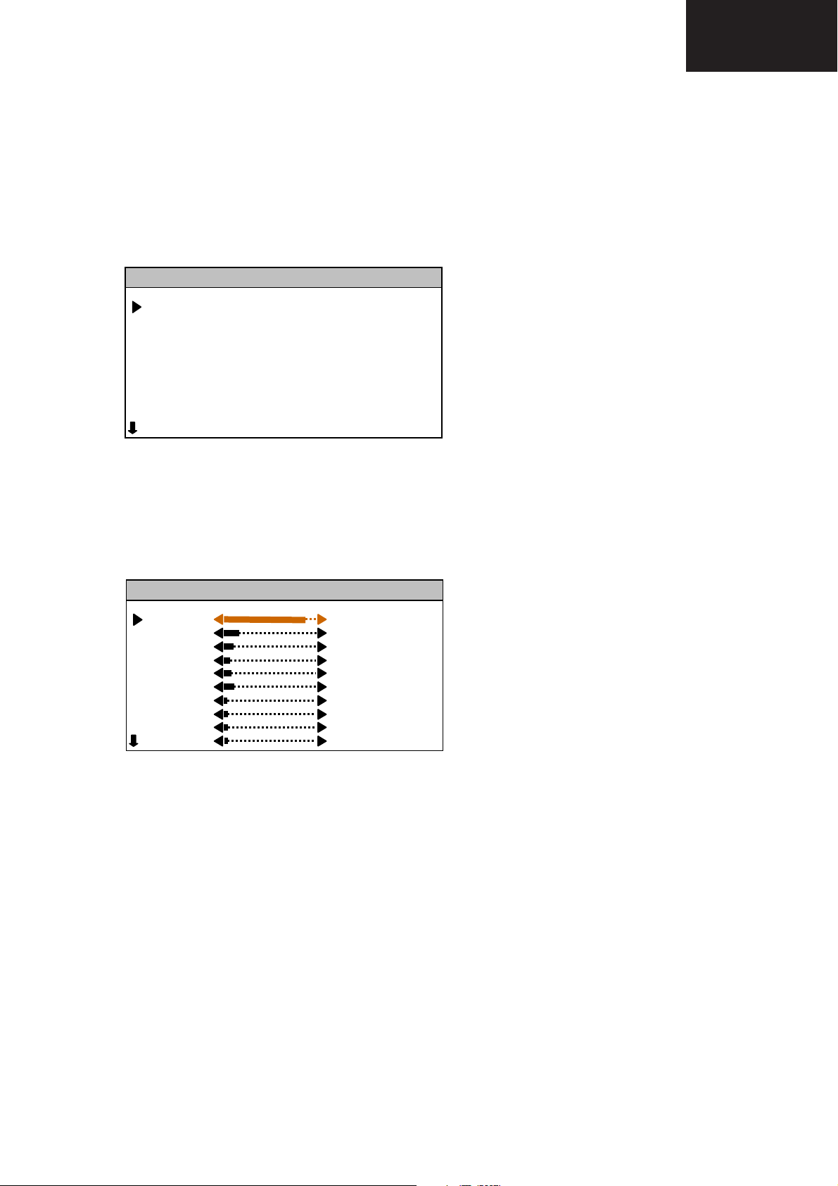
14.2.ADJUST MENU
Select the parameter by pressing up/down buttons. Adjust the parameter by pressing Left/Right
buttons. In ADJUST menu, changed values are stored automatically.
000 255
001 036
002 019
003 020
004 030
005 026
006 003
007 004
008 005
009 005
White Point Red, White Point Green, White Point Blue:
Not used.
AGC
Apply PAL BG signal, VHF-3 Channel-12 and 60dBµV signal level. Adjust AGC (Automatic Gain
Control) item by pressing Left/Right buttons till the voltage at AGC point (pin1 of the tuner) becomes 3.0
volts.
If PLL negative
Not used.
If PLL positive
Not used.
Y-Delay
Enter a PAL B/G colour and black-white bar test pattern via RF. Adjust Y-Delay for PAL till the colour
transients on the colour bar of the pattern become as sharper and colours between transients do not
mix with each other as possible.
SERVICE
AK45JA0XX
AK45JA0XX
ADJUST...
23

AK - 45
CHASSIS
Y-Delay SECAM
Enter a SECAM B/G colour and black-white bar test pattern via RF. Adjust Y-Delay SECAM till the
colour transients on the colour bar of the pattern become as sharper and colours between transients do
not mix with each other as possible.
Y-Delay NTSC
Enter an NTSC colour and black-white bar test pattern via RF. Adjust Y-Delay NTSC till the colour
transients on the colour bar of the pattern become as sharper and colours between transients do not
mix with each other as possible.
Y-Delay other
Not used.
Vertical Position Offset
This value is fixed (127)
Vertical Position Offset
This value is fixed (127)
Horizontal Position Offset
This value is fixed (127)
Horizontal Position Offset
This value is fixed (127)
Vertical Blank Start
This register will be used only at 4:3 tubes for 16:9 mode adjustment. It adjusts the vertical blank start
position.
Vertical Blank Stop
This register will be used only at 4:3 tubes for 16:9 mode adjustment. It adjusts the vertical blank stop
position.
Angle
Change Angle by pressing Left/Right buttons till the vertical lines of the crosshatch pattern become
completely perpendicular to horizontal lines without any angle of vertical deviation. Check and readjust
ANGLE item if the adjustment becomes improper after some other geometric adjustments are done.
Bow
Change Bow by pressing Left/Right buttons till the vertical lines especially ones close to the left and
right sides will of equal and symmetrical bending, i.e. they together will neither be towards left side nor
right side. Check and readjust BOW item if the adjustment becomes improper after some other
geometric adjustments are done.
4:3 Horizontal Blank Start
This register will be used only at 16:9 tube for 4:3 mode adjustment. It adjusts the horizontal blank start
position.
4:3 Horizontal Blank Stop
This register will be used only at 16:9 tube for 4:3 mode adjustment. It adjusts the horizontal blank stop
position.
EHTV Compensation
It’s used to adjust the EHT compensation vertical gain coefficient.
EHTTM Compensation
It’s used to adjust the EHT compensation time constant.
EHTEW Compensation
It’s used to adjust the EHT compensation east/west gain coefficient.
24

AK - 45
j
CHASSIS
WDR
The amplitude of R of RGB output can be adjusted with the drive parameter WDR.
WDG
The amplitude of G of RGB output can be adjusted with the drive parameter WDG.
WDB
The amplitude of B of RGB output can be adjusted with the drive parameter WDB.
CR
The DC offset values of R of RGB output can be adjusted with the cutoff parameter CR.
CG
The DC offset values of G of RGB output can be adjusted with the cutoff parameter CG.
CB
The DC offset values of B of RGB output can be adjusted with the cutoff parameter CB.
COR coring level
The amplitude of the correction signal is adjustable. Small noise amplitudes in the correction signal are
suppressed by an adjustable coring circuit.
REGULAR VERT_POS (Regular mode Vertical Position)
Enter a PAL B/G circle test pattern via RF. Change Vertical Position till the test pattern is vertically
centered. Horizontal line at the center pattern is in equal distance both to upper and lower side of the
picture tube. Check and readjust Vertical Position item if the adjustment becomes improper after some
other geometric adjustments are done.
It’s used to adjust the vertical position of regular mode.
REGULAR VERT_AMPL (Regular mode Vertical Amplitude)
It’s used to adjust the vertical amplitude of regular mode.
REGULAR VERT_SCOR (Regular mode Vertical S-Correction)
It’s used to adjust the vertical s-correction of regular mode.
REGULAR VERT_SSYM(Regular mode Vertical S Symmetry)
It’s used to adjust the vertical s-symmetry of regular mode.
REGULAR TRAPEZE (Regular mode Trapeze)
Change Trapezium by pressing Left/Right buttons till vertical lines, especially lines at the sides of the
picture frame became parallel to the both sides of picture tube as close as possible. Check and readjust
TRPEZ item if the adjustment becomes improper after some other geometric adjustments are done.
It’s used to adjust the trapeze of regular mode.
REGULAR CUSHION (Regular mode Cushion)
It’s used to adjust the cushion of regular mode.
REGULAR HOR_COR_SYM (Regular mode Horizontal Corner Symmetry)
It’s used to adjust the horizontal corners symmetry of regular mode.
REGULAR HOR_CORNER (Regular mode Horizontal Corner)
It’s used to adjust the horizontal corners of regular mode.
REGULAR HORZ_POS (Regular mode Horizontal Position)
Enter a PAL B/G circle test pattern via RF. Change Horizontal Position until the picture is horizontally
centered. Check and readjust Horizontal Position item if the adjustment becomes improper after some
other geometric adjustments are done.
It’s used to adjust the horizontal position of regular mode.
REGULAR HORZ_AMPL (Regular mode Horizontal Amplitude)
It’s used to ad
ust the horizontal amplitude of regular mode.
25

AK - 45
CHASSIS
PANORAMIC VERT_POS (Panoramic mode Vertical Position)
It’s used to adjust the vertical position of panoramic mode.
PANORAMIC VERT_AMPL (Panoramic mode Vertical Amplitude)
It’s used to adjust the vertical amplitude of panoramic mode.
PANORAMIC VERT_SCOR (Panoramic mode Vertical S-Correction)
It’s used to adjust the vertical s-correction of panoramic mode.
PANORAMIC VERT_SSYM (Panoramic mode Vertical S-Symmetry)
It’s used to adjust the vertical s-symmetry of panoramic mode.
PANORAMIC TRAPEZE (Panoramic mode Trapeze)
It’s used to adjust the trapeze of panoramic mode.
PANORAMIC CUSHION (Panoramic mode Cushion)
It’s used to adjust the cushion of panoramic mode.
PANORAMIC HOR_COR_SYM (Panoramic mode Horizontal corner symmetry)
It’s used to adjust the horizontal corners symmetry of panoramic mode.
PANORAMIC HOR_CORNER (Panoramic mode Horizontal corner)
It’s used to adjust the horizontal corners of panoramic mode.
PANORAMIC HORZ_POS (Panoramic mode Horizontal position)
It’s used to adjust the horizontal position of panoramic mode.
PANORAMIC HORZ_AMPL (Panoramic mode Horizontal amplitude)
It’s used to adjust the horizontal amplitude of panoramic mode.
14:9 ZOOM VERT_POS (14:9 Zoom mode Vertical Position)
It’s used to adjust the vertical position of 14:9 zoom mode.
14:9 ZOOM VERT_AMPL (14:9 Zoom mode Vertical Amplitude)
It’s used to adjust the vertical amplitude of 14:9 zoom mode.
14:9 ZOOM VERT_SCOR (14:9 Zoom mode Vertical S-Correction)
It’s used to adjust the vertical s-correction of 14:9 zoom mode.
14:9 ZOOM VERT_SSYM (14:9 Zoom mode Vertical S-Symmetry)
It’s used to adjust the vertical s-symmetry of 14:9 zoom mode.
14:9 ZOOM TRAPEZE (14:9 Zoom mode Trapeze)
It’s used to adjust the trapeze of 14:9 zoom mode.
14:9 ZOOM CUSHION (14:9 Zoom mode Cushion)
It’s used to adjust the cushion of 14:9 zoom mode.
14:9 ZOOM HOR_COR_SYM (14:9 Zoom mode Corner Symmetry)
It’s used to adjust the horizontal corners symmetry of 14:9 zoom mode.
14:9 ZOOM HOR_CORNER (14:9 Zoom mode Horizontal Corner)
It’s used to adjust the horizontal corners of 14:9 zoom mode.
14:9 ZOOM HORZ_POS (14:9 Zoom mode Horizontal Position)
It’s used to adjust the horizontal position of 14:9 zoom mode.
14:9 ZOOM HORZ_AMPL (14:9 Zoom mode Horizontal Amplitude)
It’s used to adjust the horizontal amplitude of 14:9 zoom mode.
26

AK - 45
CHASSIS
16:9 ZOOM VERT_POS (16:9 Zoom mode Vertical Position)
It’s used to adjust the vertical position of 16:9 zoom mode.
16:9 ZOOM VERT_AMPL (16:9 Zoom mode Vertical Amplitude)
It’s used to adjust the vertical amplitude of 16:9 zoom mode.
16:9 ZOOM VERT_SCOR (16:9 Zoom mode Vertical S-Correction)
It’s used to adjust the vertical s-correction of 16:9 zoom mode.
16:9 ZOOM VERT_SSYM (16:9 Zoom mode Vertical S-Symmetry)
It’s used to adjust the vertical s-symmetry of 16:9 zoom mode.
16:9 ZOOM TRAPEZE (16:9 Zoom mode Trapeze)
It’s used to adjust the trapeze of 16:9 zoom mode.
16:9 ZOOM CUSHION (16:9 Zoom mode Cushion)
It’s used to adjust the cushion of 16:9 zoom mode.
16:9 ZOOM HOR_COR_SYM (16:9 Zoom mode Horizontal corner symmetry)
It’s used to adjust the horizontal corners symmetry of 16:9 zoom mode.
16:9 ZOOM HOR_CORNER (16:9 Zoom mode Horizontal corner)
It’s used to adjust the horizontal corners of 16:9 zoom mode.
16:9 ZOOM HORZ_POS (16:9 Zoom mode Horizontal position)
It’s used to adjust the horizontal position of 16:9 zoom mode.
16:9 ZOOM HORZ_AMPL (16:9 Zoom mode Horizontal amplitude)
It’s used to adjust the horizontal amplitude of 16:9 zoom mode.
16:9 ZOOM SUBTITLE VERT_POS (16:9 Zoom Subtitle mode Vertical position)
It’s used to adjust the vertical position of 16:9 zoom subtitle mode.
16:9 ZOOM SUBTITLE VERT_AMPL (16:9 Zoom Subtitle mode Vertical amplitude)
It’s used to adjust the vertical amplitude of 16:9 zoom subtitle mode.
16:9 ZOOM SUBTITLE VERT_SCOR (16:9 Zoom Subtitle mode Vertical S-Correction)
It’s used to adjust the vertical s-correction of 16:9 zoom subtitle mode.
16:9 ZOOM SUBTITLE VERT_SSYM (16:9 Zoom Subtitle mode Vertical S-Symmetry)
It’s used to adjust the vertical s-symmetry of 16:9 zoom subtitle mode.
16:9 ZOOM SUBTITLE TRAPEZE (16:9 Zoom Subtitle mode Trapeze)
It’s used to adjust the trapeze of 16:9 zoom subtitle mode.
16:9 ZOOM SUBTITLE CUSHION (16:9 Zoom Subtitle mode Cushion)
It’s used to adjust the cushion of 16:9 zoom subtitle mode.
16:9 ZOOM SUBTITLE HOR_COR_SYM (16:9 Zoom Subtitle mode Horizontal Corner Symmetry)
It’s used to adjust the horizontal corners symmetry of 16:9 zoom subtitle mode.
16:9 ZOOM SUBTITLE HOR_CORNER (16:9 Zoom Subtitle mode Horizontal corner)
It’s used to adjust the horizontal corners of 16:9 zoom subtitle mode.
16:9 ZOOM SUBTITLE HORZ_POS (16:9 Zoom Subtitle mode Horizontal position)
It’s used to adjust the horizontal position of 16:9 zoom subtitle mode.
16:9 ZOOM SUBTITLE HORZ_AMPL (16:9 Zoom Subtitle mode Horizontal amplitude)
It’s used to adjust the horizontal amplitude of 16:9 zoom subtitle mode.
27

AK - 45
CHASSIS
OSD Position
It’s used to adjust the horizontal position of the OSD.
BCLTHR
Beam current threshold
BCLG
Beam current loop gain
ROTATION (TILT)
This adjustment only works when the TV has rotation option. Change TILT by pressing Left/Right
buttons to rotate the complete raster clock-wise and counter clock-wise depending on the CRT. Check
and readjust TRPEZ item if the adjustment becomes improper after some other geometric adjustments
are done.
LSLSA, LSLSB, LSL2, LSLTA, LSLTB (Luma soft limiter)
LSLSA: Luma soft limiter slope A (fixed)
LSLSB: Luma soft limiter slope B (fixed)
LSL2: Luma soft limiter absolute limit (fixed)
LSLTA: L
LSLTB: L
REFERENCE WDR RED (NORMAL)
The amplitude of R of RGB output can be adjusted with the drive parameter WDR for the colour
temperature of normal mode.
REFERENCE WDR GREEN (NORMAL)
The amplitude of G of RGB output can be adjusted with the drive parameter WDR for the colour
temperature of normal mode.
REFERENCE WDR BLUE (NORMAL)
The amplitude of B of RGB output can be adjusted with the drive parameter WDR for the colour
temperature of normal mode.
REFERENCE CUTOFF RED
It’s fixed.
REFERENCE CUTOFF GREEN
It’s fixed.
REFERENCE CUTOFF BLUE
It’s fixed.
IBRM
Internal Brightness, the brightness for measurement can be set to measure at higher cutoff current. The
measurement brightness is independent of the drive values. It’s used to adjust the maximum brightness
level.
WDRV
White drive measurement control. It is used to adjust the maximum contrast level.
ACC_SAT (COLOUR OFFSET)
It’s used to adjust the max. colour level.
G2 CUTOFF REFERENCE
It’s fixed.
G2 WDR REFERENCE
It’s fixed.
uma soft limiter segment A tilt point (fixed)
uma soft limiter segment A tilt point (fixed)
28

AK - 45
CHASSIS
POFS2 (RGB HORIZONTAL SHIFT)
It’s used to adjust the horizontal position of RGB signal.
REFERENCE WDR RED COOL
The amplitude of R of RGB output can be adjusted with the drive parameter WDR for the colour temp of
cool mode.
REFERENCE WDR GREEN COOL
The amplitude of G of RGB output can be adjusted with the drive parameter WDR for the colour temp
of cool mode.
REFERENCE WDR BLUE COOL
The amplitude of B of RGB output can be adjusted with the drive parameter WDR for the colour temp of
cool mode.
REFERENCE WDR RED WARM
The amplitude of R of RGB output can be adjusted with the drive parameter WDR for the colour temp of
warm mode.
REFERENCE WDR GREEN WARM
The amplitude of G of RGB output can be adjusted with the drive parameter WDR for the colour temp
of cool mode.
REFERENCE WDR BLUE WARM
The amplitude of B of RGB output can be adjusted with the drive parameter WDR for the colour temp of
cool mode.
STANDARD MODE BRIGHTNESS
It’s used to adjust the brightness value of standard mode.
STANDARD MODE COLOUR
It’s used to adjust the colour value of standard mode.
STANDARD MODE CONTRAST
It’s used to adjust the contrast value of standard mode.
FULL VERT_POS (16:9 MODE)
It’s used to adjust the vertical position of 16:9 mode (full mode).
FULL VERT_AMPL
It’s used to adjust the vertical amplitude of 16:9 mode (full mode).
FULL VERT_SCOR
It’s used to adjust the vertical s-correction of 16:9 mode (full mode).
FULL VERT_SSYM
It’s used to adjust the vertical s-symmetry of 16:9 mode (full mode).
FULL TRAPEZE
It’s used to adjust the trapeze of 16:9 mode (full mode).
FULL CUSHION
It’s used to adjust the cushion of 16:9 mode (full mode).
FULL HOR_COR_SYM
It’s used to adjust the horizontal corners symmetry of 16:9 mode (full mode).
FULL HOR_CORNER
It’s used to adjust the horizontal corners of 16:9 mode (full mode).
29

AK - 45
CHASSIS
FULL HORZ_POS
It’s used to adjust the horizontal position of 16:9 mode (full mode).
FULL HORZ_AMPL
It’s used to adjust the horizontal amplitude of 16:9 mode (full mode).
BRIGHT MODE BRIGHTNESS
It’s used to adjust the brightness value of bright mode.
BRIGHT MODE COLOUR
It’s used to adjust the colour value of bright mode.
BRIGHT MODE CONTRAST
It’s used to adjust the contrast value of bright mode.
SOFT MODE BRIGHTNESS
It’s used to adjust the brightness value of soft mode.
SOFT MODE COLOUR
It’s used to adjust the colour value of soft mode.
SOFT MODE CONTRAST
It’s used to adjust the contrast value of soft mode.
PERSONAL MODE FACTORY SETTING BRIGHTNESS
It’s fixed.
PERSONAL MODE FACTORY SETTING COLOUR
It’s fixed.
PERSONAL MODE FACTORY SETTING CONTRAST
It’s fixed.
SCINC FOR PANORAMIC MODE
scaler1 coefficient, this scaler is compressing the signal.
SCINC1 FOR PANORAMIC MODE
scaler2 coefficient, this scaler is expanding the signal.
VOLUME AFTER APS
It’s used to adjust the volume level after APS.
VERTICAL SCROLL
It’s used to adjust the step width for scroll function.
14:9 HORIZONTAL START
It’s used to adjust the horizontal blank start position for 14:9 mode.
14:9 HORIZONTAL STOP
It’s used to adjust the horizontal blank stop position for 14:9 mode.
4:3 RGB HORIZONTAL AMPLITUDE
It’s used to adjust the horizontal amplitude in 4:3 mode for RGB signals.
4:3 RGB CUSHION
It’s used to adjust the cushion in 4:3 mode for RGB signals.
14:9 RGB HORIZONTAL AMPLITUDE
It’s used to adjust the horizontal amplitude in 14:9 mode for RGB signals.
30

14:9 RGB CUSHION
It’s used to adjust the cushion in 14:9 mode for RGB signals.
PANORAMIC RGB HORIZONTAL AMPLITUDE
It’s used to adjust the horizontal amplitude in panoramic mode for RGB signals.
16:9 RGB HORIZONTAL AMPLITUDE
It’s used to adjust the horizontal amplitude in 16:9 mode for RGB signals.
16:9 SUBTITLE RGB HORIZONTAL AMPLITUDE
It’s used to adjust the horizontal amplitude in 16:9 subtitle mode for RGB signals.
FULL RGB HORIZONTAL AMPLITUDE
It’s used to adjust the horizontal amplitude in full mode for RGB signals.
TELETEXT HORZ_POS
It’s used to adjust the horizontal position of teletext signal.
AK - 45
CHASSIS
31

AK - 45
CHASSIS
SHARP 11AK45 TVs ADJUST VALUES
SETTING VALUES
ADJUST
N0
ADJUST 0 Not used 255 255 255
ADJUST 1 Not used 36 36 36
ADJUST 2 Not used 19 19 19
ADJUST 3 AGC (Autamatic Gain Control)
ADJUST 4 Not used 30 30 30
ADJUST 5 Not used 26 26 26
ADJUST 6 Y-Delay 2 2 2
ADJUST 7 Y-Delay SECAM 3 3 3
ADJUST 8 Y-Delay NTSC 5 5 5
ADJUST 9 Y-Delay OTHER 5 5 5
ADJUST 10 Vertical Position Offset 127 127 127
ADJUST 11 Vertical Amplitude Offset 127 127 127
ADJUST 12 Horizontal Position Offset 127 127 127
ADJUST 13 Horizontal Amplitude Offset 127 127 127
ADJUST 14
ADJUST 15
ADJUST 16 Angle 129 124 139
ADJUST 17 Bow 131 127 127
ADJUST 18
ADJUST 19
ADJUST 20 EHTV compensation 66 55 66
ADJUST 21 EHTTM compensation 2 2 5
ADJUST 22 EHTEW compensation 160 219 160
ADJUST 23 WDR
ADJUST 24 WDG
ADJUST 25 WDB
ADJUST 26 CR
ADJUST 27 CG
ADJUST 28 CB
ADJUST 29 COR coring level 15
ADJUST 30 NORMAL VERT_POS 127 128 127
ADJUST 31 NORMAL VERT_AMPL 53 81 53
ADJUST 32 NORMAL VERT_SCOR 129 132 133
ADJUST 33 NORMAL VERT_SSYM 136 136 131
ADJUST 34 NORMAL TRAPEZE 129 129 131
ADJUST 35 NORMAL CUSHION 149 155 141
ADJUST 36 NORMAL HOR_COR_SYM 128 123 118
ADJUST 37 NORMAL HOR_CORNER 113 107 137
ADJUST 38 NORMAL HORZ_POS 50 54 45
ADJUST 39 NORMAL HORZ_AMPL 98 16 107
ADJUST 40 PANORAMIC VERT_POS 127 127
ADJUST 41 PANORAMIC VERT_AMPL 52 48
ADJUST 42 PANORAMIC VERT_SCOR 134 133
ADJUST 43 PANORAMIC VERT_SSYM 139 131
ADJUST 44 PANORAMIC TRAPEZE 129 131
ADJUST 45 PANORAMIC CUSHION 150 146
ADJUST 46 PANORAMIC HOR_COR_SYM 134 121
ADJUST 47 PANORAMIC HOR_CORNER 113 134
ADJUST 48 PANORAMIC HORZ_POS 48 48
ADJUST 49 PANORAMIC HORZ_AMPL 36 44
ADJUST 50 ZOOM 14:9 VERT_POS 128 125
ADJUST 51 ZOOM 14:9 VERT_AMPL 41 42
ADJUST 52 ZOOM 14:9 VERT_SCOR 134 133
ADJUST 53 ZOOM 14:9VERT_SSYM 140 131
ADJUST 54 ZOOM 14:9 TRAPEZE 128 131
ADJUST 55 ZOOM 14:9 CUSHION 156 148
ADJUST 56 ZOOM 14:9 HOR_COR_SYM 145 123
ADJUST 57 ZOOM 14:9 HOR_CORNER 113 135
ADJUST 58 ZOOM 14:9 HORZ_POS 49 47
Vertical Blank Start
(It will be used only at 4.3 tube for 16:9 mode
adjustment)
Vertical Blank Stop
(It will be used only at 4.3 tube for 16:9 mode
adjustment)
Horz. Blank Start
(It will be used only at 16:9 tube for 4:3 and
14:9 mode adjustments)
Horz. Blank Stop
(It will be used only at 16:9 tube for 4:3 and
14:9 mode adjustments)
EXPLANATION
THOMSON
28'' 16:9 SF TV
W66EJU023X215
It will be adjusted to below 1V of max. AGC for each TV
No use 150 119
No use 12 34
19 No use 19
201 No use 201
THOMSON
28" 4:3 SF
A66EHJ13X01
VDP ADJUSTS ITSELF
VDP ADJUSTS ITSELF
VDP ADJUSTS ITSELF
VDP ADJUSTS ITSELF
VDP ADJUSTS ITSELF
VDP ADJUSTS ITSELF
THOMSON
32" 16:9 SF
W7EGV023X215
32

SHARP 11AK45 TVs ADJUST VALUES
)
SETTING VALUES
ADJUST
N0
ADJUST 59 ZOOM 14:9 HORZ_AMPL 59 63
ADJUST 60 CINEMA VERT_POS 128 127
ADJUST 61 CINEMA VERT_AMPL 28 32
ADJUST 62 CINEMA VERT_SCOR 129 126
ADJUST 63 CINEMA VERT_SSYM 146 131
ADJUST 64 CINEMA TRAPEZE 128 130
ADJUST 65 CINEMA CUSHION 164 154
ADJUST 66 CINEMA HOR_COR_SYM 135 128
ADJUST 67 CINEMA HOR_CORNER 117 131
ADJUST 68 CINEMA HORZ_POS 48 48
ADJUST 69 CINEMA HORZ_AMPL 36 44
ADJUST 70 16:9 ZOOM SUBTITLE VERT_POS 147 145
ADJUST 71 16:9 ZOOM SUBTITLE VERT_AMPL 33 39
ADJUST 72 16:9 ZOOM SUBTITLE VERT_SCOR 123 133
ADJUST 73 16:9 ZOOM SUBTITLE VERT_SSYM 156 129
ADJUST 74 16:9 ZOOM SUBTITLE TRAPEZE 121 122
ADJUST 75 16:9 ZOOM SUBTITLE CUSHION 162 152
ADJUST 76 16:9 ZOOM SUBTITLE HOR_COR_SYM 125 128
ADJUST 77 16:9 ZOOM SUBTITLE HOR_CORNER 114 125
ADJUST 78 16:9 ZOOM SUBTITLE HORZ_POS 48 44
ADJUST 79 16:9 ZOOM SUBTITLE HORZ_AMPL 36 43
ADJUST 80 OSD Position 205 217 205
ADJUST 81 BCLTHR beam current threshold 30 39 74
ADJUST 82 BCLG beam current loop gain 6 7 7
ADJUST 83 ROTATION (TILT) 2 2 2
ADJUST 84 LSLSA luma soft limiter 2 2 2
ADJUST 85 LSLSB 0 0 0
ADJUST 86 LSL2 255 255 255
ADJUST 87 LSLTA 0 0 0
ADJUST 88 LSLTB 1 1 0
ADJUST 89 REFERENCE WDR RED (NORMAL) X X X
ADJUST 90 REFERENCE WDR GREEN (NORMAL) X X X
ADJUST 91 REFERENCE WDR BLUE (NORMAL) X X X
ADJUST 92 REFERENCE CUTOFF RED 55 65 55
ADJUST 93 REFERENCE CUTOFF GREEN 69 68 69
ADJUST 94 REFERENCE CUTOFF BLUE 69 77 69
ADJUST 95 IBRM 215 200 215
ADJUST 96 WDRV 68 75 68
ADJUST 97 ACC_SAT (COLOR OFFSET) 130 154 130
ADJUST 98 G2 CUTOFF REFERENCE 220 200 220
ADJUST 99 G2 WDR REFERENCE 90 90 90
ADJUST 100 ADJUST POFS2 (RGB HORIZONTAL SHIFT
ADJUST 101 REFERENCE WDR RED COOL X X X
ADJUST 102 REFERENCE WDR GREEN COOL X X X
ADJUST 103 REFERENCE WDR BLUE COOL X X X
ADJUST 104 REFERENCE WDR RED WARM X X X
ADJUST 105 REFERENCE WDR GREEN WARM X X X
ADJUST 106 REFERENCE WDR BLUE WARM X X X
ADJUST 107 STANDARD MODE BRIGHTNESS 32 32 32
ADJUST 108 STANDARD MODE COLOR 47 47 47
ADJUST 109 STANDARD MODE CONTRAST 32 32 32
ADJUST 110 FULL VERT_POS 128 126 126
ADJUST 111 FULL VERT_AMPL 51 94 53
ADJUST 112 FULL VERT_SCOR 132 132 133
ADJUST 113 FULL VERT_SSYM 139 131 131
ADJUST 114 FULL TRAPEZE 128 129 129
ADJUST 115 FULL CUSHION 151 143 144
ADJUST 116 FULL HOR_COR_SYM 134 129 128
ADJUST 117 FULL HOR_CORNER 49 114 135
ADJUST 118 FULL HORZ_POS 35 54 46
ADJUST 119 FULL HORZ_AMPL 30 16 46
ADJUST 120 BRIGHT MODE BRIGHTNESS 43 43 43
ADJUST 121 BRIGHT MODE COLOR 50 50 50
ADJUST 122 BRIGHT MODE CONTRAST 32 32 32
ADJUST 123 SOFT MODE BRIGHTNESS 43 43 43
ADJUST 124 SOFT MODE COLOR 58 58 58
ADJUST 125 SOFT MODE CONTRAST 20 20 20
EXPLANATION
THOMSON
28'' 16:9 SF TV
W66EJU023X215
60 50 60
THOMSON
28" 4:3 SF
A66EHJ13X01
THOMSON
32" 16:9 SF
W7EGV023X215
AK - 45
CHASSIS
33

AK - 45
CHASSIS
SHARP 11AK45 TVs ADJUST VALUES
SETTING VALUES
ADJUST
N0
PERSONAL MODE FACTORY
ADJUST 126
ADJUST 127
ADJUST 128
ADJUST 129 SCINC FOR PANORAMIC MODE 56 56 56
ADJUST 130 SCINC1 FOR PANORAMIC MODE 125 125 125
ADJUST 131 VOLUME AFTER APS 5
ADJUST 132 VERTICAL SCROLL 11 11 11
ADJUST 133
ADJUST 134
ADJUST 135 NORMAL RGB HORIZONTAL AMPLITUDE 99 19 98
ADJUST 136 NORMAL RGB CUSHION 151 159 142
ADJUST 137 14:9 RGB HORIZONTAL AMPLITUDE 70 No use 71
ADJUST 138 14:9 RGB CUSHION 156 No use 149
ADJUST 139
ADJUST 140
ADJUST 141
ADJUST 142 FULL RGB HORIZONTAL AMPLITUDE 40 18 48
ADJUST 143 TELETEXT HORZ_POS 95 104 98
ADJUST 144 RGB BRIGHTNESS OFFSET 0 80 0
ADJUST 145 RGB CONTRAST OFFSET 0 75 0
ADJUST 146 TELETEXT BRIGHTNESS 100 150 100
ADJUST 147 TELETEXT CONTRAST 120 135 120
ADJUST 148 SVG1 3 3 3
ADJUST 149 SVD1 7 7 7
ADJUST 150 SVLIM 127 127 127
ADJUST 151 SVDEL 4 4 4
ADJUST 152 SVCOR 0 0 0
ADJUST 153
ADJUST 154
ADJUST 155
ADJUST 156
ADJUST 157 PøP BRIGHTNESS 5 5 5
ADJUST 158 PøP CONTRAST 15 15 15
SETTING BRIGHTNESS
PERSONAL MODE FACTORY
SETTING COLOR
PERSONAL MODE FACTORY
SETTING CONTRAST
14:9 HORIZONTAL START
(It will be used only at 4.3 tube for 16:9 mode
adjustment)
14:9 HORIZONTAL STOP
(It will be used only at 4.3 tube for 16:9 mode
adjustment)
PANORAMIC RGB
HORIZONTAL AMPLITUDE
CINEMA RGB
HORIZONTAL AMPLITUDE
ZOOM 16:9 SUBTITLE RGB
HORIZONTAL AMPLITUDE
RASTER Horz. Blank Start
(It will be used only at 16:9 tube for 4:3 and
14:9 mode adjustments)
RASTER Horz. Blank Stop
(It will be used only at 16:9 tube for 4:3 and
14:9 mode adjustments)
RASTER RGB Horz. Blank Start
(It will be used only at 16:9 tube for 4:3 and
14:9 mode adjustments)
RASTER RGB Horz. Blank Stop
(It will be used only at 16:9 tube for 4:3 and
14:9 mode adjustments)
EXPLANATION
THOMSON
28'' 16:9 SF TV
W66EJU023X215
32 32 32
47 47 47
32 32 32
19 No use 19
201 No use 201
40 No use 49
40 No use 48
40 No use 48
117 No use 115
178 No use 176
116 No use 116
177 No use 176
THOMSON
28" 4:3 SF
A66EHJ13X01
THOMSON
32" 16:9 SF
W7EGV023X215
X: WILL BE ADJUSTED AUTOMATICALLY ACCORDING TO THE SHARP SPECIFICATION.
COLOR TEMPERATURE SHOULD BE (SHARP SPECIFICATION);
FOR NORMAL (x, y) (290, 300) (304, 306) (290, 284)
FOR COOL (x, y) (274, 273) (288, 269) (274, 257)
FOR WARM (x, y) (310, 294) (324, 300) (310, 278)
WESTERN EUROPE EASTERN EUROPE UK
34

AK - 45
CHASSIS
14.3.OPTIONS MENU
Select the parameter by pressing up/down buttons. Adjust the parameter by pressing Left/Right
buttons. . In OPTIONS menu, some of the changed parameters are not stored automatically. To store
the adjusted parameters, you should turn off and on TV.
000 02
001 00
002 22
003 08
004 00
005 10
006 00
007 56
008 39
009 0F
Option 0. Video Processor Crystal Indication
B7: x = x
B6: x = x
B5: x = x
B4: x = x
B3: x = x
B2: x = x
B1: Xa = note1 (Crystal indication)
B0: Xb = note1 (Crystal indication)
note 1:
Xa,Xb
0,1 : Pal M, Pal N, NTSC M
Pin 34 : 3.58 (1, 2 or 3 crystals)
Pin 35 : No crystal
1,0 : Pal BG, Pal DK, Pal I/I+, Secam BG, Secam DK, Secam L/L’, Secam K1
Pin 34 : No crystal
Pin 35 : 4.43 (1 crystal)
1,1 : Pal BG, Pal DK, Pal I/I+, Secam BG, Secam DK, Secam L/L’, Secam K1, Pal M, Pal N, Ntsc M
Pin 34 : 3.58 (1, 2 or 3 crystals)
Pin 35 : 4.43 (1 crystal)
OPTIONS...
00000010
00000000
00100010
00001000
00000000
00010000
00000000
01010110
00111001
00001111
Option 1. (0x01) Video Processor Decoder Mode Register
B7: x = x
B6: x = x
B5: x = x
B4: x = x
B3: x = x
B2: x = x
B1: x = x
B0: x = x
Option 2. (0x18) Video Processor Blanking Control
B7: SWF = 1 (Subwoofer item at menu)
B6: Vsd = 0 (Vertical scan disable)
B5: x = x
35

AK - 45
CHASSIS
B4: x = x
B3: x = x
B2: x = x
B1: LUMA = 1 Luma Soft Limiter Enabled
B0: BB = 1 Blue Background Option
Option 3. (0x19) Video Processor Cathode Drive Level
B7: x = x
B6: x = x
B5: x = x
B4: x = x
B3: x = x
B2: x = x
B1: x = x
B0: country = note 0
Note 0: choice for others country option
1 : BG
0 : DK
Option 4.
B7: x = x
B6: x = x
B5: x = x
B4: x = x
B3: x = x
B2: x = x
B1: x = x
B0: x = x
Option 5. CTI Available, Mono AVL
B7: x = x
B6: x = x
B5: x = x
B4: x = x
B3: x = x
B2: x = x
B1: x = x
B0: x = x
Option 6.
B7: = TEXT LANGUAGE 3
B6: = TEXT LANGUAGE 2
B5: = TEXT LANGUAGE 1
B4: x = x
B3: x = x
B2: x = x
B1: x = x
B0: x = x
Option 7. OPTIONHOTELACTIVE, PLL_VST, PIP Zoom Mode, PIP Position
B7: x = x
B6: x = x
B5: F = note 1
B4: x = x
B3: x = x
B2: PZM = x
B1: AV2 = 1 AV2 Output enabled
B0: x = x
36

Note 1:
F :Frequency Mode
1: = Frequency Menu Item available
0: = Frequency Menu Item not available
Option 8. IF Frequency
B7: x = x
B6: x = x
B5: IfI = 0 note 3
B4: IfD = 0 note 4
B3: IfM = note 5
B2: Aps = note 6
B1: Hp = note 7
B0: Hue = note 8
Note 3:
IfI
1 = IF I 39.5 MHz Great Britain I , Only UHF Tuner
0 = IF I 38.9 MHz Ireland I+ , Standard Tuner
Note 4:
IfD
1 = IF DK 38.0 MHz
0 = IF DK 38.9 MHz
Note 5:
IfM
1 = IF M,N 45.75 MHz S&N American Models , Tuner UV1336 (Only Pal M/N, Ntsc M)
0 = IF M,N 38.9 MHz Euro M,N Models , Standard Tuner
Note 6:
Aps ( Only for PLL )
0 = A.P.S. done
1 = A.P.S. set
Note 7:
Hp : Headphone available
0 = No headphone
1 = Headphone available
Note 8:
Hue : Hue Available
0 = No Hue
1 = Hue available
AK - 45
CHASSIS
Option 9. Standard Available
B7: NM = note 1
B6: PN = note 1
B5: PM = note 1
B4: K1 = note 1
B3: L = note 1
B2: I = note 1
B1: DK = note 1
B0: BG = note 1
Note 1:
0 = Standard not supported
1 = Standard available
37

AK - 45
CHASSIS
Option 10. Scart, Combfilter, Teletext, Language
B7: x = x
B6: RGB = note 2
B5: FAV =
B4: AV2S =
B3: FSVHS = note 3
B2: BAV = note 4
B1: Sc2 = note 5
B0: BSVHS = note 6
Note 2 :
RGB = RGB Menu Item active/inactive
0 = RGB Menu Item inactive
1 = RGB Menu Item active
Note 3:
0 = Front S-VHS not supported
1 = Front S-VHS available
Note 4:
0 = Back AV (AV-3) not supported
1 = Back AV (AV-3) available
Note 5:
0 = Scart 2 not supported
1 = Scart 2 available
Note 6:
0 = Back SVHS not supported
1 = Back SVHS available
Option 11. PLL Tuner Control 1 Byte
Pll tuner control 1 byte
b7 b6 b5 b4 b3 b2 b1 b0
Philips UV1316T MK3 1 0 0 0 1 1 1 0
Philips UV1316MK2 1 0 0 0 1 1 1 0
Alps TELE9X062A 1 0 0 0 1 1 1 0
Samsung TEXX2949PG28A 1 0 0 0 1 1 1 0
Siel PT060 1 0 0 0 1 1 1 0
Temic 5001PH5-3X0003 1 0 0 0 1 1 1 0
Thomson CTT5020 1 0 0 0 1 1 1 0
Option 12. PLL Tuner Control 2 Low Byte
Pll tuner control 2 low byte
b7 b6 b5 b4 b3 b2 b1 b0
Philips UV1316T MK3 0 0 0 0 0 0 0 1
Philips UV1316MK2 1 0 1 0 0 0 0 1
Alps TELE9X062A 0 0 0 0 0 0 0 1
Samsung TEXX2949PG28A 0 0 0 0 0 0 0 1
Siel PT060 0 1 1 0 0 0 0 0
Temic 5001PH5-3X0003 0 0 0 0 0 0 1 0
Thomson CTT5020 0 0 0 0 0 0 1 1
38

Option 13. PLL Tuner Control 2 Mid Byte
b7 b6 b5 b4 b3 b2 b1 b0
Philips UV1316T MK3 0 0 0 0 0 0 1 0
Philips UV1316MK2 1 0 0 1 0 0 1 0
Alps TELE9X062A 0 0 0 0 0 0 1 0
Samsung TEXX2949PG28A 0 0 0 0 0 0 1 0
Siel PT060 1 1 0 1 0 0 0 0
Temic 5001PH5-3X0003 0 0 0 0 0 1 0 0
Thomson CTT5020 0 0 0 0 0 1 1 0
Option 14. PLL Tuner Control 2 High Byte
b7 b6 b5 b4 b3 b2 b1 b0
Philips UV1316T MK3 0 0 0 0 0 1 0 0
Philips UV1316MK2 0 0 1 1 0 1 0 0
Alps TELE9X062A 0 0 0 0 1 0 0 0
Samsung TEXX2949PG28A 0 0 0 0 1 0 0 0
Siel PT060 0 0 1 1 0 0 0 0
Temic 5001PH5-3X0003 0 0 0 0 0 0 0 1
Thomson CTT5020 1 0 0 0 0 1 0 1
AK - 45
CHASSIS
Option 15. PLL Tuner VHF LOW – VHF HIGH Crossover Low Byte
b7 b6 b5 b4 b3 b2 b1 b0
Philips UV1316T MK3 0 0 1 0 0 0 0 0
Philips UV1316MK2 0 0 0 0 1 0 1 0 (0A hex)
Alps TELE9X062A 0 0 0 0 0 0 0 0
Samsung TEXX2949PG28A 0 0 0 0 1 0 0 0
Siel PT060 0 0 0 0 1 0 1 0
Temic 5001PH5-3X0003 0 0 0 0 0 0 0 0
Thomson CTT5020 1 0 1 0 1 0 1 0 (AA hex)
Option 16. PLL Tuner VHF LOW – VHF HIGH Crossover High Byte
Pll tuner VHF LOW - VHF HIGH crossover high byte
b7 b6 b5 b4 b3 b2 b1 b0
Philips UV1316T MK3 0 0 0 0 1 1 0 0
Philips UV1316MK2 0 0 0 0 1 1 0 0 (0C hex)
Alps TELE9X062A 0 0 0 0 0 0 0 0
Samsung TEXX2949PG28A 0 0 0 0 1 1 0 1
Siel PT060 0 0 0 0 1 1 0 1
Temic 5001PH5-3X0003 0 0 0 0 0 0 0 0
Thomson CTT5020 0 0 0 0 1 0 0 1 (09 hex)
Option 17. PLL Tuner VHF HIGH – UHF Crossover Low Byte
b7 b6 b5 b4 b3 b2 b1 b0
Philips UV1316T MK3 0 0 0 0 0 0 1 0
Philips UV1316MK2 1 1 1 0 0 0 1 0 (E2 hex)
Alps TELE9X062A 0 0 0 0 0 0 0 0
Samsung TEXX2949PG28A 1 0 1 0 0 0 1 0
Siel PT060 1 0 1 0 0 1 0 0
Temic 5001PH5-3X0003 0 0 0 0 0 0 0 0
Thomson CTT5020 1 0 1 0 0 0 1 0 (A2 hex)
Option 18. PLL Tuner VHF HIGH – UHF Crossover High Byte
b7 b6 b5 b4 b3 b2 b1 b0
Philips UV1316T MK3 0 0 0 1 1 1 1 0
Philips UV1316MK2 0 0 0 1 1 1 1 0 (1D hex)
Alps TELE9X062A 0 0 0 0 0 0 0 0
Samsung TEXX2949PG28A 0 0 0 1 1 1 1 0
Siel PT060 0 0 0 1 1 1 1 0
39

AK - 45
CHASSIS
Temic 5001PH5-3X0003 0 0 0 0 0 0 0 0
Thomson CTT5020 0 0 0 1 1 0 1 1 (1B hex)
Option 19. PIP PLL Tuner Control 1 Byte
b7 b6 b5 b4 b3 b2 b1 b0
Philips UV1316MK2 1 0 0 0 1 1 1 0
Alps TELE9X062A 1 0 0 0 1 1 1 0
Samsung TEXX2949PG28A 1 0 0 0 1 1 1 0
Siel PT060 1 0 0 0 1 1 1 0
Temic 5001PH5-3X0003 1 0 0 0 1 1 1 0
Thomson CTT5020 1 0 0 0 1 1 1 0
Option 20. PIP PLL Tuner Control 2 Low Byte
b7 b6 b5 b4 b3 b2 b1 b0
Philips UV1316MK2 1 0 1 0 0 0 0 1
Alps TELE9X062A 0 0 0 0 0 0 0 1
Samsung TEXX2949PG28A 0 0 0 0 0 0 0 1
Siel PT060 0 1 1 0 0 0 0 0
Temic 5001PH5-3X0003 0 0 0 0 0 0 1 0
Thomson CTT5020 0 0 0 0 0 0 1 1
Option 21. PIP PLL Tuner Control 2 Mid Byte
b7 b6 b5 b4 b3 b2 b1 b0
Philips UV1316MK2 1 0 0 1 0 0 1 0
Alps TELE9X062A 0 0 0 0 0 0 1 0
Samsung TEXX2949PG28A 0 0 0 0 0 0 1 0
Siel PT060 1 1 0 1 0 0 0 0
Temic 5001PH5-3X0003 0 0 0 0 0 1 0 0
Thomson CTT5020 0 0 0 0 0 1 1 0
Option 22. PIP PLL Tuner Control 2 High Byte
b7 b6 b5 b4 b3 b2 b1 b0
Philips UV1316MK2 0 0 1 1 0 1 0 0
Alps TELE9X062A 0 0 0 0 1 0 0 0
Samsung TEXX2949PG28A 0 0 0 0 1 0 0 0
Siel PT060 0 0 1 1 0 0 0 0
Temic 5001PH5-3X0003 0 0 0 0 0 0 0 1
Thomson CTT5020 1 0 0 0 0 1 0 1
Option 23. PIP PLL Tuner VHF LOW – VHF HIGH Crossover Low Byte
b7 b6 b5 b4 b3 b2 b1 b0
Philips UV1316MK2 0 0 0 0 1 0 1 0 (0A hex)
Alps TELE9X062A 0 0 0 0 0 0 0 0
Samsung TEXX2949PG28A 0 0 0 0 1 0 0 0
Siel PT060 0 0 0 0 1 0 1 0
Temic 5001PH5-3X0003 0 0 0 0 0 0 0 0
Thomson CTT5020 1 0 1 0 1 0 1 0 (AA hex)
Option 24. PIP PLL Tuner VHF LOW – VHF HIGH Crossover High Byte
b7 b6 b5 b4 b3 b2 b1 b0
Philips UV1316MK2 0 0 0 0 1 1 0 0 (0C hex)
Alps TELE9X062A 0 0 0 0 0 0 0 0
Samsung TEXX2949PG28A 0 0 0 0 1 1 0 1
Siel PT060 0 0 0 0 1 1 0 1
Temic 5001PH5-3X0003 0 0 0 0 0 0 0 0
Thomson CTT5020 0 0 0 0 1 0 0 1 (09 hex)
40

Option 25. PIP PLL Tuner VHF HIGH – UHF Crossover Low Byte
p
b7 b6 b5 b4 b3 b2 b1 b0
Philips UV1316MK2 1 1 1 0 0 0 1 0 (E2 hex)
Alps TELE9X062A 0 0 0 0 0 0 0 0
Samsung TEXX2949PG28A 1 0 1 0 0 0 1 0
Siel PT060 1 0 1 0 0 1 0 0
Temic 5001PH5-3X0003 0 0 0 0 0 0 0 0
Thomson CTT5020 1 0 1 0 0 0 1 0 (A2 hex)
Option 26. PIP PLL Tuner VHF HIGH – UHF Crossover High Byte
b7 b6 b5 b4 b3 b2 b1 b0
Philips UV1316MK2 0 0 0 1 1 1 1 0 (1D hex)
Alps TELE9X062A 0 0 0 0 0 0 0 0
Samsung TEXX2949PG28A 0 0 0 1 1 1 1 0
Siel PT060 0 0 0 1 1 1 1 0
Temic 5001PH5-3X0003 0 0 0 0 0 0 0 0
Thomson CTT5020 0 0 0 1 1 0 1 1 (1B hex)
Option 27. Language Available 1
B7: L7 = DANISH
B6: L6 = SWEDISH
B5: L5 = ITALIAN
B4: L4 = PORTUGUESE
B3: L3 = SPANISH
B2: L2 = FRENCH
B1: L1 = GERMAN
B0: L0 = ENGLISH
1: Language available
0: Language not available
AK - 45
CHASSIS
Option 28. Language Available 2
B7: L15 = CROATIC
B6: L14 = POLISH
B5: L13 = SLOVAK
B4: L12 = CZECH
B3: L11 = HUNGARY
B2: L10 = GREEK
B1: L9 = TURKEY
B0: L8 = NORWEGIAN
1: Language available
0: Language not available
Option 29. Language Available 3 and Zoom Mode Available
B7: ZSP = 16:9 ZOOM SUBTITLE MODE
B6: ZSB = 16:9 ZOOM MODE
B5: ZCN = 14:9 ZOOM MODE
B4: PNM = 1 (Panoramic zoom mode)
B3: Tub = note 2
B2: Z.Def = note 3
B1: PMK = note 1
B0:
1: Available
0: Not available
Note 1 :
PMK : Picture mode key
0 : Not available picture mode key from RC
1 : available
icture mode key from RC
41

AK - 45
CHASSIS
Note 2:
Tub : Tube size
0 = 16:9 Tube size
1 = 4:3 Tube size
Note 3:
Z.Def : Zoom Default Mode
0 = 16:9 mode default
1 = 4:3 mode default
Option 30. Country
B7: C4 = note 1
B6: C3 = note 1
B5: C2 = note 1
B4: C1 = note 1
B3: C0 = note 1
B2: x = x
B1: x = x
B0: x = x
Note 1:
C5,C4,C3,C2,C1,C0 = Country
0, 0, 0,0,0 = OTHER, Not allowed
0, 0, 0,0,1 = D, Germany
0, 0, 0,1,0 = A,
0, 0, 0,1,1 = CH,
0, 0, 1,0,0 = I,
0, 0, 1,0,1 = F,
0, 0, 1,1,0 = RSM,
0, 0, 1,1,1 = B,
0, 1, 0,0,0 = DK,
0, 1, 0,0,1 = S,
0, 1, 0,1,0 = N,
0, 1,0,1,1 = FIN,
0, 1,1,0,0 = GB,
0, 1,1,0,1 = IRL,
0, 1,1,1,0 = IS,
0, 1,1,1,1 = NL,
1, 0,0,0,0 = E,
1, 0,0,0,1 = P,
1, 0,0,1,0 = PL,
1, 0,0,1,1 = CZ,
1, 0,1,0,0 = H,
1, 0,1,0,1 = HR,
1, 0,1,1,0 = GR,
1, 0,1,1,1 = TR
Option 31. Prescaler MSP FM (AVL=OFF)
b7 b6 b5 b4 b3 b2 b1 b0
Prescaler MSP FM (AVL = OFF) 0 0 0 0 1 0 0 0
b7 b6 b5 b4 b3 b2 b1 b0
Prescaler MSP FM (AVL = OFF) 0 0 0 0 1 0 0 0 (if virtual Dolby option is available)
Option 32. Prescaler MSP NICAM (AVL=OFF)
b7 b6 b5 b4 b3 b2 b1 b0
Prescaler MSP NICAM (AVL = OFF) 0 0 0 1 1 1 1 1
42

b7 b6 b5 b4 b3 b2 b1 b0
Prescaler MSP NICAM (AVL = OFF) 0 0 0 1 1 1 1 1 (if virtual Dolby option is available)
Option 33. Prescaler MSP SCART (AVL=OFF)
b7 b6 b5 b4 b3 b2 b1 b0
Prescaler MSP SCART (AVL = OFF) 0 0 0 0 1 1 0 0
b7 b6 b5 b4 b3 b2 b1 b0
Prescaler MSP SCART (AVL = OFF) 0 0 0 1 1 0 0 1 (if virtual Dolby option is available)
Option 34. Prescaler MSP I2S (AVL=OFF)
b7 b6 b5 b4 b3 b2 b1 b0
Prescaler MSP I2S (AVL = OFF) not defined yet
(if virtual Dolby option is available)
Option 35. Not used
B7: x = note 7
B6: x = note 6
B5: x = note 5
B4: x = note 4
B3: AV2S = Scart2 SVHS
B2: Macro = Macrovision
B1: DP = Dolby Prologic
B0: VD = Virtual Dolby
AK - 45
CHASSIS
Option 36. Not used
B7: x = note 7
B6: TAT = 1 Tilt and trapeze enabled
B5: SWF = 1 Subwoofer enabled
B4: VLO = 1 Variable line out
B3: VBUS = 1 Vestelbus enabled
B2: x = x
B1: DVD = 1 DVD enabled
B0: DVB = 1 DVB enabled
Option 37. Reserved for USA
Option 38. TV Teletext Mode Selection, Child Lock, Equalizer Country
B7: VCR = note 7
B6: C = note 6
B5: LM = note 5
B4: EQ = note 4
B3: x = x
B2: CL = note 2
B1: T1 = note 1
B0: T0 = note 1
Note 1:
Teletext selection
T1, T0:
0,0 = No TV Text
0,1 = Simple TV Text (One page)
1,1 = Fasttext/Toptext TV Text (Eight pages)
Note 2:
CL = Child Lock
0 = Off
1 = On (Active)
43

AK - 45
CHASSIS
Note 3:
RGB = RGB Menu Item active/inactive
0 = RGB Menu Item inactive
1 = RGB Menu Item active
Note 4:
EQ = Equalizer available
0 = Equalizer not available
1 = Equalizer available
Note 5:
LM = List Mode available
0 = List Mode not available
1 = List Mode available
Note 6:
C = Country Line available / Aps available or not
0 = Country Line not available / Aps not available
1 = Country Line available / Aps available
Note 7:
VCR = VCR Menu Item available / not available
0 = VCR Menu Item not available
1 = VCR Menu Item available
Option 39. Personal Preference Equalizer Band 1
b7 b6 b5 b4 b3 b2 b1 b0
EQUALIZER BAND 1 0 0 0 0 0 1 1 0
Option 40. Personal Preference Equalizer Band 2
b7 b6 b5 b4 b3 b2 b1 b0
EQUALIZER BAND 2 0 0 0 0 0 1 1 0
Option 41. Personal Preference Equalizer Band 3
b7 b6 b5 b4 b3 b2 b1 b0
EQUALIZER BAND 3 0 0 0 0 0 1 1 0
Option 42. Personal Preference Equalizer Band 4
b7 b6 b5 b4 b3 b2 b1 b0
EQUALIZER BAND 4 0 0 0 0 0 1 1 0
Option 43. Personal Preference Equalizer Band 5
b7 b6 b5 b4 b3 b2 b1 b0
EQUALIZER BAND 5 0 0 0 0 0 1 1 0
Option 44. Sound Effect (Standard; Music; Speech; Jazz; Pp)
b7 b6 b5 b4 b3 b2 b1 b0
SOUND EFFECT 0 0 0 0 0 1 1 0
Option 45. Volume Offset Left
b7 b6 b5 b4 b3 b2 b1 b0
VOLUME OFFSET LEFT 0 0 0 0 0 1 1 0
Option 46. Volume Offset Right
b7 b6 b5 b4 b3 b2 b1 b0
VOLUME OFFSET RIGHT 0 0 0 0 0 1 1 0
44

Option 47. Volume Offset Center
b7 b6 b5 b4 b3 b2 b1 b0
VOLUME OFFSET CENTER 0 0 0 0 0 1 1 0
Option 48. Volume Offset Rear
b7 b6 b5 b4 b3 b2 b1 b0
VOLUME OFFSET REAR 0 0 0 0 0 1 1 0
Option 49. Surround Delay
b7 b6 b5 b4 b3 b2 b1 b0
SURROUND DELAY 0 0 0 0 0 0 0 1
Option 50. FM Prescaler
b7 b6 b5 b4 b3 b2 b1 b0
FM PRESCALER for Stereo 0 0 0 0 1 1 0 0
b7 b6 b5 b4 b3 b2 b1 b0
FM PRESCALER for Dolby 0 0 0 0 1 0 0 1
Note: if virtual Dolby is available, this option is not used.
AK - 45
CHASSIS
Option 51. NICAM Prescaler
b7 b6 b5 b4 b3 b2 b1 b0
NICAM Prescaler for Stereo 0 0 1 0 1 1 0 1
b7 b6 b5 b4 b3 b2 b1 b0
3D Panorama 0 0 0 0 1 0 1 1
b7 b6 b5 b4 b3 b2 b1 b0
NICAM Prescaler for Dolby 0 0 0 0 1 1 1 0
Note: if virtual Dolby is available, this option is not used.
Option 52. Scart Input Prescaler
b7 b6 b5 b4 b3 b2 b1 b0
Scart Input Prescaler for Stereo 0 0 0 0 1 0 0 0
b7 b6 b5 b4 b3 b2 b1 b0
Scart Input Prescaler for Dolby 0 0 0 0 1 1 1 1
b7 b6 b5 b4 b3 b2 b1 b0
Prescaler MSP Scart (AVL = OFF) 0 0 0 1 1 0 0 1 (if virtual Dolby option is available)
Note: if virtual Dolby is available, this option is not used.
Option 53. I2S Prescaler
b7 b6 b5 b4 b3 b2 b1 b0
I2S Prescaler for Stereo 0 0 0 0 0 1 1 0
b7 b6 b5 b4 b3 b2 b1 b0
I2S Prescaler for Dolby 0 0 0 0 0 1 1 0
Note: if virtual Dolby is available, this option is not used.
Option 54. Scart Output Prescaler
b7 b6 b5 b4 b3 b2 b1 b0
Scart Output Prescaler 0 1 1 1 1 1 1 1
45

AK - 45
CHASSIS
Option 55. Speaker Setup
b7 b6 b5 b4 b3 b2 b1 b0
Speaker Setup (L/R, L/C/R, L/R/S, L/C/R/S) 0 0 0 0 0 0 0 0
Option 56. Audio Options Available Or Not
Attention: All bits on the Option 56 must be the “0” for MONO TV SETS
B7: Nicam = note 7
B6: ASD = note 6
B5: VRS = note 5
B4: CRM = note 4
B3: … = x
B2: LBE = note 2
B1: Spa = note 1
B0: Avl = note 0
Note 7:
Nicam = Nicam available
0 = Nicam not available
1 = Nicam available
Note 6:
ASD = Auto Sound Detection available/not available
0 = Auto Sound Detection not available
1 = Auto Sound Detection available
Note 5:
VRS = Virtual Surround
0 = VRS not available
1 = VRS available
Note 4:
CRM = CARRIER MUTE OFF/ON
0 = Sound carrier mute is ON in the Stereo Sound IC
1 = Sound carrier mute is OFF in the Stereo Sound IC (i.e. option available)
Note 2:
LBE = LBE (Dynamic Bass)
0 = LBE not available
1 = LBE available
Note 1:
Spa = Spatial Effect available
0 = Spatial Effect not available
1 = Spatial Effect available
Note 0:
Avl = Automatic volume level available on the Menu
0 = Automatic volume level not available
1 = Automatic volume level available
Option 57. Stereo Threshold
B7: b7 = note 1 Remark:
B6: b6 = note 1
B5: b5 = note 1 -Threshold for all FM A2 signals to switch from MONO to STEREO.
B4: b4 = note 1 -For first check after programme change half value is changed (0Ch) 19h/2
B3: b3 = note 1 -For switching from STEREO back to MONO: 19h/4 *3
B2: b2 = note 1
B1: b1 = note 1
B0: b0 = note 1
46

Note 1:
b7 b6 b5 b4 b3 b2 b1 b0
MSP Stereo/Mono Threshold 0 0 0 1 1 0 0 1
Option 58. MSP Audio Flags
B7: b7 = x
B6: b6 = x
B5: b5 = x
B4: Trs = note 1
B3: Trb = note 1
B2: Bbe = note 1
B1: Spa = note 1
B0: Avl = note 1
Note 1:
Defines whether the feature is toggled ON or OFF in the menu and stored.
0 : OFF
1 : ON
Option 59. NICAM Threshold
b7 b6 b5 b4 b3 b2 b1 b0
MSP NICAM Threshold 0 1 1 0 0 1 0 0
AK - 45
CHASSIS
Option 60. Power Delay Time
B7: NZ = x
B6: HM = x
B5: L5 = note 3
B4: L4 = note 3
B3: L3 = note 3
B2: L2 = note 3
B1: L1 = note 3
B0: L0 = note 3
Note 3:
L7 L6 L5 L4 L3 L2 L1 L0
Default Value: x x 1 1 0 0 0 0
1000 MSEC = 1SN
Number
L7L6L5L4L3L2L1L0
Delay Number
L7L6L5L4L3L2L1L0
Delay
0 00000000 = 4 Sec 32 00100000 = 12 Sec
1 00000001 = 4,25 Sec 33 00100001 = 12,25 Sec
2 00000010 = 4,5 Sec 34 00100010 = 12,5 Sec
3 00000011 = 4,75 Sec 35 00100011 = 12,75 Sec
4 00000100 = 5 Sec 36 00100100 = 13 Sec
5 00000101 = 5,25 Sec 37 00100101 = 13,25 Sec
6 00000110 = 5,5 Sec 38 00100110 = 13,5 Sec
7 00000111 = 5,75 Sec 39 00100111 = 13,75 Sec
8 00001000 = 6 Sec 40 00101000 = 14 Sec
9 00001001 = 6,25 Sec 41 00101001 = 14,25 Sec
10 00001010 = 6,5 Sec 42 00101010 = 14,5 Sec
11 00001011 = 6,75 Sec 43 00101011 = 14,75 Sec
12 00001100 = 7 Sec 44 00101100 = 15 Sec
13 00001101 = 7,25 Sec 45 00101101 = 15,25 Sec
14 00001110 = 7,5 Sec 46 00101110 = 15,5 Sec
15 00001111 = 7,75 Sec 47 00101111 = 15,75 Sec
16 00010000 = 8 Sec 48 00110000 = 16 Sec
17 00010001 = 8,25 Sec 49 00110001 = 16,25 Sec
18 00010010 = 8,5 Sec 50 00110010 = 16,5 Sec
19 00010011 = 8,75 Sec
51 00110011 = 16,75 Sec
47

AK - 45
CHASSIS
20 00010100 = 9 Sec 52 00110100 = 17 Sec
21 00010101 = 9,25 Sec 53 00110101 = 17,25 Sec
22 00010110 = 9,5 Sec 54 00110110 = 17,5 Sec
23 00010111 = 9,75 Sec 55 00110111 = 17,75 Sec
24 00011000 = 10 Sec 56 00111000 = 18 Sec
25 00011001 = 10,25 Sec 57 00111001 = 18,25 Sec
26 00011010 = 10,5 Sec 58 00111010 = 18,5 Sec
27 00011011 = 10,75 Sec 59 00111011 = 18,75 Sec
28 00011100 = 12 Sec 60 00111100 = 19 Sec
29 00011101 = 12,25 Sec 61 00111101 = 19,25 Sec
30 00011110 = 12,5 Sec 62 00111110 = 19,5 Sec
31 00011111 = 12,75 Sec
63 00111111 = 19,75 Sec
48

AK - 45
CHASSIS
Decimal - Binary Conversion Table
76543210
0 00000000 32 00100000
1 00000001 33 00100001
2 00000010 34 00100010
3 00000011 35 00100011
4 00000100 36 00100100
5 00000101 37 00100101
6 00000110 38 00100110
7 00000111 39 00100111
8 00001000 40 00101000
9 00001001 41 00101001
10 00001010 42 00101010
11 00001011 43 00101011
12 00001100 44 00101100
13 00001101 45 00101101
14 00001110 46 00101110
15 00001111 47 00101111
16 00010000 48 00110000
17 00010001 49 00110001
18 00010010 50 00110010
19 00010011 51 00110011
20 00010100 52 00110100
21 00010101 53 00110101
22 00010110 54 00110110
23 00010111 55 00110111
24 00011000 56 00111000
25 00011001 57 00111001
26 00011010 58 00111010
27 00011011 59 00111011
28 00011100 60 00111100
29 00011101 61 00111101
30 00011110 62 00111110
31 00011111
Bit Position
76543210
63 00111111
49

AK - 45
CHASSIS
14.4.OPTION TABLE RECOMMENDED VALUES
X listed in the option can be 0 or 1
OPTION 28" 4:3 MULTI 28" 16:9 MULTI 28" 16:9 PAL I
000 X2 XXXXXX10 X2 XXXXXX10 X2 XXXXXX10
001 XX XXXXXXXX XX XXXXXXXX XX XXXXXXXX
002 23 001XXX11 23 001XXX11 23 001XXX11
003 XX XXXXXXX0 XX XXXXXXX0 XX XXXXXXX0
004 XX XXXXXXXX XX XXXXXXXX XX XXXXXXXX
005 XX XXXXXXXX XX XXXXXXXX XX XXXXXXXX
006 XX XXXXXXXX XX XXXXXXXX XX XXXXXXXX
007 XX XX0XXX1X XX XX0XXX1X XX XX0XXX1X
008 A1 11000001 01 00000001 01 00000001
009 0B 00001111 0B 00001111 04 00001111
010 X2 XXXXX011 X7 XXXXX111 X7 XXXXX111
011 8E 10001110 8E 10001110 8E 10001110
012 03 00000011 03 00000011 03 00000011
013 06 00000110 06 00000110 06 00000110
014 15 10000101 15 10000101 15 10000101
015 AA 10101010 AA 10101010 AA 10101010
016 09 00001001 09 00001001 09 00001001
017 A2 10100010 A2 10100010 A2 10100010
018 1B 00011011 1B 00011011 1B 00011011
019 XX XXXXXXXX XX XXXXXXXX XX XXXXXXXX
020 XX XXXXXXXX XX XXXXXXXX XX XXXXXXXX
021 XX XXXXXXXX XX XXXXXXXX XX XXXXXXXX
022 XX XXXXXXXX XX XXXXXXXX XX XXXXXXXX
023 XX XXXXXXXX XX XXXXXXXX XX XXXXXXXX
024 XX XXXXXXXX XX XXXXXXXX XX XXXXXXXX
025 XX XXXXXXXX XX XXXXXXXX XX XXXXXXXX
026 XX XXXXXXXX XX XXXXXXXX XX XXXXXXXX
027 FF 11111111 FF 11111111 FF 11111111
028 FF 11111111 FF 11111111 FF 11111111
029 FF 11111111 EF 11101111 EF 11101111
030 XX XXXXXXX XX XXXXXXX XX XXXXXXX
031 0F 00001111 0F 00001111 0F 00001111
032 23 00100011 23 00100011 23 00100011
033 0E 00001110 0E 00001110 0E 00001110
034 XX XXXXXXXX XX XXXXXXXX XX XXXXXXXX
035 XX XXXXXXXX XX XXXXXXXX XX XXXXXXXX
036 X4 XXXXX1XX X4 XXXXX1XX X4 XXXXX1XX
037 XX XXXXXXXX XX XXXXXXXX XX XXXXXXXX
038 AF 11001111 AF 11001111 AF 11001111
039 XX XXXXXXXX XX XXXXXXXX XX XXXXXXXX
040 XX XXXXXXXX XX XXXXXXXX XX XXXXXXXX
041 XX XXXXXXXX XX XXXXXXXX XX XXXXXXXX
042 XX XXXXXXXX XX XXXXXXXX XX XXXXXXXX
043 XX XXXXXXXX XX XXXXXXXX XX XXXXXXXX
044 XX XXXXXXXX XX XXXXXXXX XX XXXXXXXX
045 XX XXXXXXXX XX XXXXXXXX XX XXXXXXXX
046 XX XXXXXXXX XX XXXXXXXX XX XXXXXXXX
047 XX XXXXXXXX XX XXXXXXXX XX XXXXXXXX
048 XX XXXXXXXX XX XXXXXXXX XX XXXXXXXX
049 XX XXXXXXXX XX XXXXXXXX XX XXXXXXXX
050 XX XXXXXXXX XX XXXXXXXX XX XXXXXXXX
051 41 01000001 41 01000001 41 01000001
052 1B 00011011 1B 00011011 1B 00011011
053 06 00000110 06 00000110 06 00000110
50

054 75 01110101 75 01110101 75 01110101
055 00 00000000 00 00000000 00 00000000
056 DE 11011110 DE 11011110 DE 11011110
057 19 00011001 19 00011001 19 00011001
058 00 00000000 00 00000000 00 00000000
059 64 01100100 64 01100100 64 01100100
060 10 00010000 10 00010000 10 00010000
AK - 45
CHASSIS
51

AK - 45
CHASSIS
14.5.SCREEN ADJUSTMENT (FBT SCREEN)
SCREEN
ADJUST
POT
From the option list change option 2 bit 6 from 0 to 1 for disabling vertical scan. Adjust horizontal line
via screen adjust pot. as thin as possible. Then press 0 to leave service menu.
52

14.6.GEOMETRY ADJUSTMENT
4:3 FORMATS
AK - 45
CHASSIS
4:3 MODE
16:9 MODE
53

AK - 45
CHASSIS
16:9 FORMATS
AUTO MODE
54

REGULAR MODE
AK - 45
CHASSIS
55

AK - 45
CHASSIS
ZOOM 14:9 MODE
56

ZOOM 16:9 MODE
AK - 45
CHASSIS
57

AK - 45
CHASSIS
SUBTITLE ZOOM MODE
58

FULL MODE
AK - 45
CHASSIS
59

AK - 45
CHASSIS
PANORAMIC MODE
60

15. BLOCK DIAGRAM
General Block Diagram of chassis 11AK45
Yoke
G
B
R
Vertical Stage
STV9379FA
TDA 6107
(PHILIPS)
RGB AMPLIFIER
Horizontal
B
G
R
CRT
OSD_R
OSD_G
OSD_B
AK - 45
CHASSIS
12W
8 ohm
Headphone
L
OSD_FBL
R
AUDIO
TDA7269A
12W
8 ohm
AMPLIFIER
SC3_V_OUT
CVBS
SC1_V_OUT
QSS
TDA9885T
PIP
VDP313XY
B
R
FB
G
SCL
SDA
SYNC
SC2_V_OUT
B
R
G
FB
EXT_CVBS/Y
SDA5555
(MicroController)
SCL
SDA
CVBS_TEXT
TV_LINK
24CO8
(E2PROM)
TO_PIP
TDA1308
SCL
SDA
SC1
L
MSP34XXG
SC2
R
DVD/DVB/BAV
FRONT/SC3
EPCOS
K3958M
Video
SAW
TU200
Filter
38.9MHz-TV TUNER
K9656M
Sound
RGB SW
Filter
SAW
EPCOS
PI5V330-SOIC
SC1_RGB
SDA
SC2_RGB/DVD/DVB
SCL
SC1
TEA615C
VIDEO SW
SC2
IF
SC3
SVHS-Y
61

AK - 45
CHASSIS
16. CIRCUIT DIAGRAMS
16.1 Schematic Diagram of Video-IF Circuit
I
H
G
F
E
D
C
B
Page 63
A
1
2
3
4567
62

16.1 Schematic Diagram of Video-IF Circuit
AK - 45
CHASSIS
I
H
G
F
E
D
C
Page 62
8 9
10
B
A
11 12 13 14
63

AK - 45
CHASSIS
I
H
G
16.2 Schematic Diagram of µ-Controller Circuit
F
E
D
C
B
A
1
2
3
4567
64

16.3 Schematic Diagram of Deflection Circuit
AK - 45
CHASSIS
I
H
G
16.4 Schematic Diagram of Power Switch Circuit
F
E
D
C
8 9
11SW01-3
10
B
A
11 12 13 14
65

AK - 45
CHASSIS
I
H
G
16.5 Schematic Diagram of SMPS Circuit
F
E
D
C
B
Page 67
A
1
2
3
4567
66

16.5 Schematic Diagram of SMPS Circuit
AK - 45
CHASSIS
I
H
G
F
E
D
C
Page 66
8 9
10
B
A
11 12 13 14
67

AK - 45
CHASSIS
I
H
G
16.6 Schematic Diagram of Sound Circuit
F
E
D
C
B
Page 69
A
1
2
3
4 567
68

16.6 Schematic Diagram of Sound Circuit
AK - 45
CHASSIS
I
H
G
F
E
D
C
Page 68
8 9
10
B
A
11 12 13 14
69

AK - 45
CHASSIS
I
H
G
16.7 Schematic Diagram of CRT Socket Circuit
F
E
D
C
B
A
1
2
3
4567
70

16.8 Schematic Diagrams of Control Panel Unit
AK - 45
CHASSIS
I
H
G
F
E
D
C
8 9
10
B
A
11 12 13 14
71

AK - 45
CHASSIS
I
H
G
16.9 Schematic Diagram of Remote Control Circuit
F
E
D
C
B
A
1
2
3
4567
72

AK - 45
CHASSIS
17. HOW TO UPDATE THE TECHNICAL INFORMATION
17.1 How to update the Technical Information appeared on this Service Manual (and
relatives)
17.1.1. Web site: https://www.vestelservice.com
17.1.2.Select: Technical Support
17.1.3. Login: 101278
17.1.4. Password: SHPII278
By this access you can consult the latest schematic diagram or request the Parts Listing of a concrete Production Date / Serial Number.
By this way it can be also consulted the issued Technical Reports (Service Bulletins).
It can be found a Label in every chassis with additional information, i.e. the used EEPROM. See below.
On the next page are given details about the Code Bar Label.
17.2 NVM / EEPROM recorder
There is available the NVM / EEPROM recorder as spare part:
Part Reference: V20096887
Description: MD.ASY.PONYPROG
Dom. Price Code: AT
Exp. Price Code: BE
This EEPROM recorder uses the free software “Pony” available at http://www.lancos.com/ppwin95.html
Note: In case of Windows platform it is recomended the PonyProg v1.17h version.
17.3 Chassis Label Information
B+ Voltage
Batch number
Chassis code
number
25423426 - 150V
200101577 PAL /BG
Y237 - 1902 - 277
EEPROM number
Consecutive serial number
of the related batch
Production line
number
73

AK - 45
CHASSIS
17.4 Code Bar Label Information
Product Code
From the beginning of September.2002,
the production month and year will be
indicated inside the box as shown.
Year
Month
Year
Consecutive number
Batch number
Product code:
Year :
Month :
Batch number :
Consecutive Number:
Consecutive number
Year
It is the code that indicates Vestel internal identification
number of the complete TV set.
Production year in two digits, e.g.: 02 for 2002
Production month in two digits; e.g.: 04 for April.
It is a Vestel number that is assigned by the Planning
Dept. according to the customer orders. (For internal
use by Vestel)
The number that indicates the sequence of the product
related to the same batch number.
74

Notes:
AK - 45
CHASSIS
75

AK - 45
CHASSIS
No part of this publication may be reproduced,
stored in a retrieval system, or transmitted in any
form or by any means, electronic, mechanical,
photocopying, recording, or otherwise, without
prior written permission of the publisher.
Technical information and Production:
Vestel Electronik AS
PRINTED BY: ON:
Technical information re-issued:
SHARP ELECTRONICA ESPAÑA S.A.
Service Manual Group
Engineering Dept.
Polígono Industrial Can Sant Joan
08190 Sant Cugat del Vallès
Barcelona
Spain
Think Ecology, please use
RECYCLED PAPER
76
 Loading...