

Datasheet X0202MA1BA2, X0205NA2BL2, X0205NA1BA2, X0205MN5BA4, X0205MA2BL2 Datasheet (SGS Thomson Microelectronics)
...
®
X02 Ser ies
SENSITIVE 1.25A SCRs
MAIN FEATURES:
Symbol Value Unit
I
T(RMS)
V
DRM/VRRM
I
GT
1.25 A
600 and 800 V
50 to 200 µA
DESCRIPTION
Thanks to highly sensitive triggering levels, the
X02 SCR series is suitable for all applications
where the available gate current is limited, such as
ground fault circuit interruptors, overvoltage
crowbar protection in low power supplies,
capacitive ignition circuits, ...
Available in though-hole or surface-mount
packages, these devices a re opt imized in forward
voltage drop and inrush current capabilities, for
reduced power los ses and high reliability in harsh
environments.
TO-92
(X02xxA)
A
G
K
SOT-223
(X02xxN)
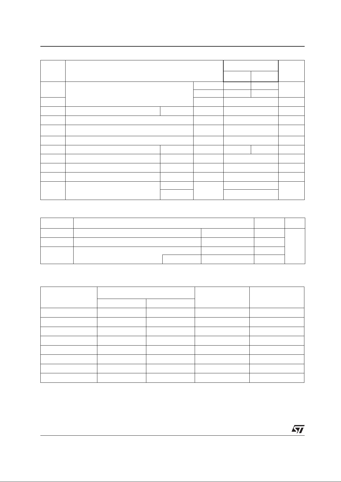
ABSOLUTE RATINGS (lim iting values)
Symbol Parameter Value Unit
I
T(RMS)
IT
(AV)
I
TSM
²
I
dI/dt
I
GM
P
G(AV)
T
stg
Tj
RMS on-state current
(180° conduction angle)
Average on-state current
(180° conduction angle)
Non repetitive surge peak on-state
current
tI
²
t Value for fusing
Critical rate of rise of on-state current
= 2 x IGT , tr ≤ 100 ns
I
G
Peak gate current tp = 20 µs Tj = 125°C 1.2 A
Average gate power dissipation Tj = 125°C 0.2 W
Storage junction temperature range
Operating junction temp erature range
September 2000 - Ed: 3
TO-92 TI = 55°C
SOT-223 Ttab = 95°C
1.25 A
TO-92 TI = 55°C
0.8 A
SOT-223 Ttab = 95°C
tp = 8.3 ms
Tj = 25°C
25
tp = 10 ms 22.5
tp = 10 ms Tj = 25°C 2.5
F = 60 Hz Tj = 125°C 50 A/µs
- 40 to + 150
- 40 to + 125
A
2
S
A
°C
1/6
X02 Series
ELECTRICAL CHARACTERISTICS (Tj = 25°C, unless otherwise specified)
Symbol Test Conditions
X02xx
02 05
I
GT
VD = 12 V RL = 140 Ω
V
GT
V
V
dV/dt V
V
V
I
DRM
I
RRM
VD = V
GD
IRG = 10 µA
RG
I
I
H
I
L
TM
to
R
= 50 mA RGK = 1 kΩ
T
IG = 1 mA RGK = 1 kΩ MAX.
= 67 % V
D
ITM = 2.5 A tp = 380 µs
Threshold voltage Tj = 125°C MAX. 0.9 V
Dynamic resistance Tj = 125°C MAX. 200 mΩ
d
V
DRM
RL = 3.3 kΩ RGK = 1 kΩ
DRM
RGK = 1 kΩ
DRM
= V
RGK = 1 kΩ
RRM
Tj = 125°C MIN.
Tj = 110°C MIN. 10 15 V/µs
Tj = 25°C MAX. 1.45 V
Tj = 25°C MAX. 5
Tj = 125°C 500
MIN. - 20
MAX. 200 50
MAX. 0.8 V
0.1 V
MIN.
8V
MAX. 5 mA
6
THERMAL RESISTANCES
Symbol Parameter Value Unit
R
R
R
th(j-l)
th(j-t)
th(j-a)
Junction to leads (DC)
TO-92 60
Junction to tab (DC) SOT-223 25
Junction to ambient (DC) TO-92 150
S = 5 cm
²
SOT-223 60
Unit
µA
mA
µA
°C/W
S = Copper surface under tab
PRODUCT SELECTOR
Part Number
600 V 800 V
X0202MA X 200 µA TO-92
X0202MN X 200 µA SOT-223
X0202NA X 200 µA TO-92
X0202NN X 200 µA SOT-223
X0205MA X 50 µA TO-92
X0205MN X 50 µA SOT-223
X0205NA X 50 µA TO-92
X0205NN X 50 µA SOT-223
2/6
Voltage
Sensitivity
Package

X02 Series
ORDERING INFORMATION
X 02 02 M A 1BA2
Blank
SENSITIVE
SCR
SERIES
CURRENT: 1.25A
SENSITIVITY:
VOLTAGE:
M: 600V
N: 800V
PACKAGE:
A:TO-92
N: SOT-223
PACKING MODE:
1BA2:TO-92 Bulk
2BL2:TO-92 Ammopack
5BA4: SOT-223 Tape & Reel
02: 200µA
05: 50µA
OTHER INFORMATION
Part Number Marking Weight Base Quantity Packing mode
X02xxyA 1BA2 X02xxyA 0.2 g 2500 Bulk
X02xxyA 2BL2 X02xxyA 0.2 g 2000 A mmop ack
X0202yN 5BA4 X2y 0.12 g 1000 Tape & reel
X0205yN 5BA4 X5y 0.12 g 1000 Tape & reel
Note: xx = sensitivity, y = voltage
Fig. 1: Maximum average power dissipation
versus average on-state current.
P(W)
1.2
1.0
0.8
0.6
0.4
0.2
0.0
0.0 0.1 0.2 0.3 0.4 0.5 0.6 0.7 0.8 0.9
IT(av)(A)
Fig. 2-1: Average and D.C. on-state current
versus lead temperature (SOT-223/TO-92).
IT(av)(A)
1.4
1.2
1.0
0.8
0.6
0.4
0.2
0.0
02550
SOT-223
TO-92
TO-92
Tlead orTlab(°C)
75
SOT-223
100 125
3/6

X02 Series
Fig. 2-2: Average and D.C. on-state current
versus ambient temperature (device mounted o n
FR4 with recommended pad layout) (SOT-223/
TO-92).
IT(av)(A)
1.4
1.2
1.0
0.8
0.6
0.4
0.2
0.0
02550
SOT-223
TO-92
SOT-223
TO-92
Tamb(°C)
75
100 125
Fig. 4: Relative variation of gate trigger current,
holding current and latching current versus
junction temperature (typical values).
IGT,IH, IL[Tj]/IGT, IH, IL[Tj] = 25°C]
1.50
1.25
1.00
0.75
0.50
0.25
0.00
-40 -20 0 20 40 60 80 100 120 140
Tj(°C)
Ω
Fig. 3: Relative variation of thermal impedance
junction to ambient versus pulse duration
(SOT-223/TO-92).
K = [Zth(j-a)/Rth(j-a)]
1.00
TO-92
0.10
0.01
1E-2 1E-1 1E+0 1E+1 1E+2 5E+2
SOT-223
tp(s)
Fig. 5: Relative variation of holding current
versus gate-cathode resistance (typical values).
IH[Rgk] / IH[Rgk = 1 kΩ]
4.0
3.5
3.0
2.5
2.0
1.5
1.0
0.5
0.0
1E-2 1E-1 1E+0 1E+1
Rgk(kΩ)
Tj = 25°C
Fig. 6: Relative variation of dV/dt immunity
versus gate-cathode resistance (typical values).
dV/dt[Rgk]/dV/dt
10.0
1.0
0.1
0.0 0.2 0.4 0.6 0.8 1.0 1.2 1.4 1.6 1.8 2.0
4/6
[
Rgk=1kΩ]
Rgk(kΩ)
Tj = 125°C
VD = 0.67xVDRM
Fig. 7: Relative variation of dV/dt immunity
versus gate-cathode capacitance (typical values).
dV/dt[Cgk] / dV/dt[Rgk = 1k ]Ω
20
18
16
14
12
10
8
6
4
2
0
0
24
6810
Cgk(nF)
12 14
16 18 20
22

X02 Series
Fig. 8: Surge peak on-state current versus
number of cycles.
ITSM(A)
25
20
Nonrepetitive
15
10
5
0
1 10 100 1000
Repetitive
Tamb=25°C
Tjinitial=25°C
tp=10ms
Onecycle
Number of cycles
Fig. 10: On-state characteristics (maximum
values).
ITM(A)
3E+1
1E+1
1E+0
1E-1
VTM(V)
2.0 2.5 3.0 3.5 4.0 4.51.51.00.5
Fig. 9: Non-repetitive surge peak on-state
current for a sinusoidal pulse with width
tp < 10 ms, and corresponding value of I²t.
ITSM(A), I t(A S)
300
100
10
1
22
tp(ms)
1.00 10.000.100.01
Fig. 11: Thermal resistance junct ion to ambient
versus copper surface under tab (Epoxy printed
circuit board FR4, copper thickness: 35 µm)
(SOT-223).
Rth(j-a) (°C/W)
130
120
110
100
90
80
70
60
50
40
30
20
10
0
S(cm )
2
4.0 4.5 5.03.53.02.52.01.51.00.50.0
PACKAGE MECHANICAL DATA
TO-92 (Plastic)
BAC
F
D
DIMENSIONS
REF .
a
Millimeters Inches
Min. Typ. Max. Min. Typ. Max.
A 1.35 0.053
B 4.70 0.185
C 2.54 0.100
D 4.40 0.173
E
E 12.70 0.500
F 3.70 0.146
a 0.50 0.019
5/6

X02 Series
PACKAGE MECHANICAL DATA
SOT-223 (Plastic)
A
A1
B
e1
D
B1
H
E
e
V
DIMENSIONS
c
REF.
Millimeters Inches
Min. Typ. Max. Min. Typ. Max.
A 1.80 0.071
A1 0.02 0.1 0.0008 0.004
B 0.60 0.70 0.85 0.024 0.027 0.034
B1 2.90 3.00 3.15 0.114 0.118 0.124
c 0.24 0.26 0.35 0.009 0.010 0.014
D 6.30 6.50 6.70 0.248 0.256 0.264
e 2.3 0.090
e1 4.6 0.181
E 3.30 3.50 3.70 0.130 0.138 0.146
H 6.70 7.00 7.30 0.264 0.276 0.287
V 10° max
FOOTPRINT DIMENSIONS (in millimete r s )
SOT-223 (Plastic)
Information furnished is believed to be accurate and reliable. However, STMicroelectronics assumes no responsibility for the consequences
of use of su ch in form at io n n or fo r a ny in fr ing eme nt of pa te nts or o ther r igh ts of th ir d pa r tie s w hic h may res ul t f rom i ts us e. No license is granted
by impl i cation or ot herwise under any patent or patent r i ght s of STMi croelectr oni cs. Specif i cations mentioned i n this publ i cation are subject
to change without noti ce. This public ation supersedes and replaces all inform ation previ ously suppli ed. STMicroel ectronic s products are not
authori zed for use as critical com ponents in li fe support devices or syst ems withou t ex press written approval of STMicroelectronics.
6/6
© The ST logo is a registered t rademark of S TMicroelectronics
© 2000 STMicroelectronics - Printed in Italy - All Rights Reserved
STMicroele ct ronics GROUP OF COMPANIES
Australia - Brazil - China - Finland - France - Germany - Hong Kong - India - Italy - Japan - Malaysia - Malta - Morocco
Singapo re - Spain - Sweden - Swit zerland - Un ited Kingd om
http://w ww.st.com
 Loading...