

Page 1
.OUTPUTCURRENT UP TO 2.5A
.WIDERANGEOFSUPPLYVOLTAGES:+8 to
+32V
.CAN WITHSTAND OVERVOLTAGES OF AS
HIGHAS 60 VBETWEEN V
ANDGROUND
CC
.INTERNAL ZENER DIODE PROVIDES FAST
SWITCHINGOF INDUCTIVELOADS
.OUTPUT VOLTAGE CAN BE LOWER THAN
GROUND
DESCRIPTION
TheTDF1778isadualsourcedriverdeliveringhigh
output currents and capable to drive any type of
loads(Electrovalves,contactors,lamps).
This deviceis essentiallyblow-outproof,each output isprotectedagainstshort-circuits.If internaldissipationbecomestoohigh,driverswillshutdownto
prevent excessive heating. An ”ALARM” output is
providedtoindicatetheactionofthethermalprotection.Toreactivatethepoweroutputs,theresetinput
mustbe forcedtolow state.
”SENSE” information of both power outputs are
ORedtogetherand thenprocessedinternally.
A ”STROBE” inputisalsoprovidedto offerthe possibilityof disablingthepoweroutputs.
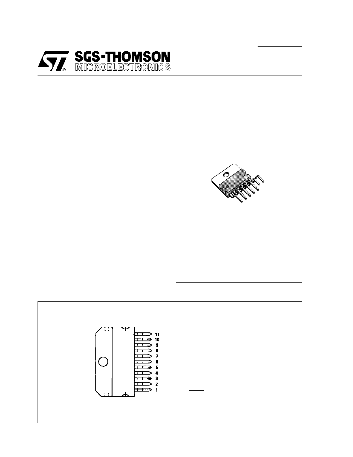
TDF1 778
DUAL 2-A SOURCE DRIVER
MULTIWATT11
ORDERING NUMBER : TDF1778SP
PIN CONNE CTION
April1993
1 - Output1
2 - VCC
3 - Output2
4 - N.C.
5 - Strobe
6 - Ground
7 - Input2
8 - Sense output
9 - Alarmoutput
10 - Resetinput
11 - Input1
1/10
Page 2
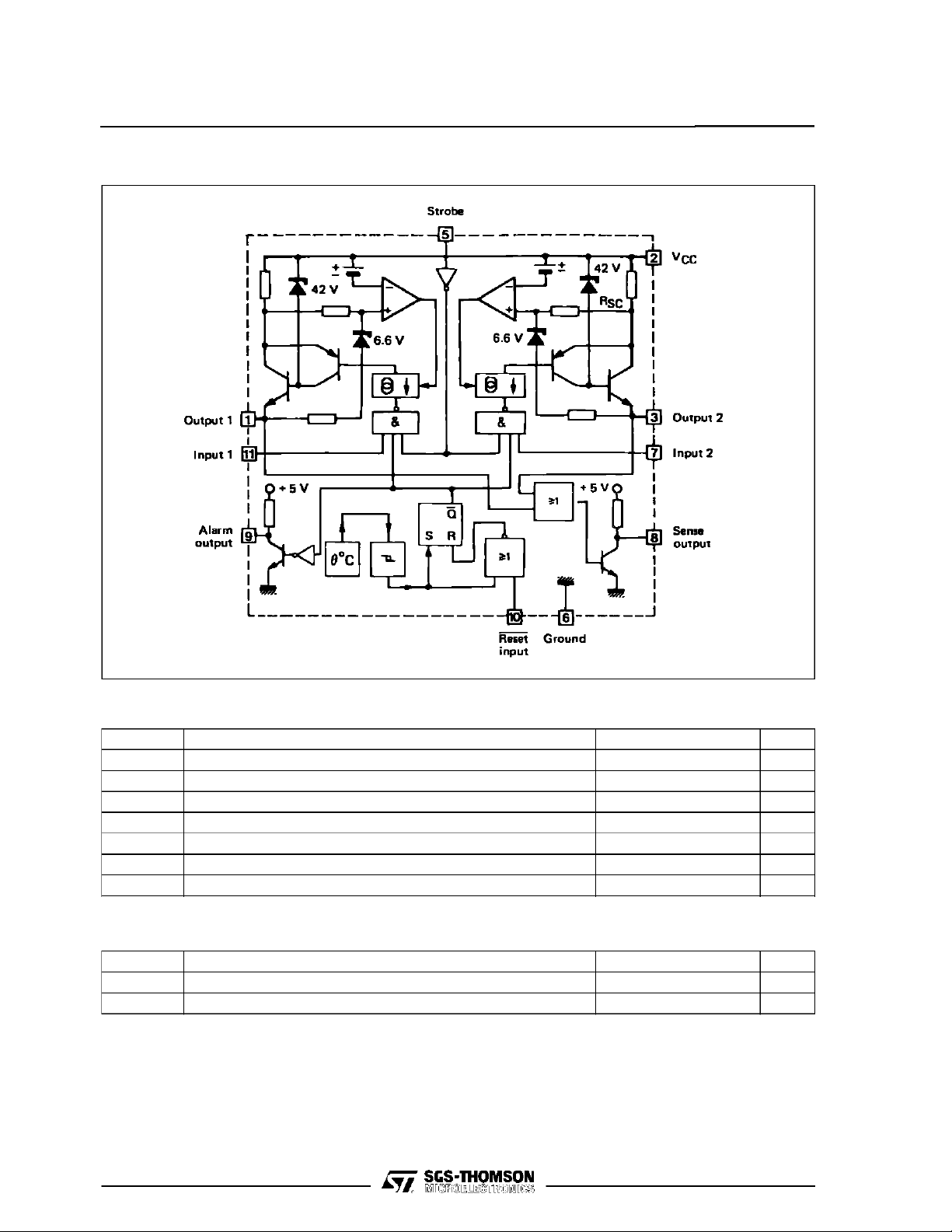
TDF1778
BLOCK DIAGRAM
ABSOLUTE MAXIMUM RATINGS
Symbol Parameter Value Unit
V
CC
V
I,Vreset
V
strobe
I
O
P
T
oper
T
tot
Supply Voltage 35 V (60 V/10 ms) V
Input Voltage (pins 7, 10 and 11) – 30 to + 50 V
Strobe Input Voltage – 0.5 to V
Output Current Internally Limited A
Power Dissipation Internally Limited W
Operating Ambient Temperature Range – 40 to + 85 °C
Junction Temperature + 150 °C
j
CC
THERMAL DATA
Symbol Parameter Value Unit
R
R
th(j–c)
th(j–a)
Junction-case Thermal Resistance Max. 3 °C/W
Junction-ambient Thermal Resistance Max. 40 °C/W
V
2/10
Page 3
TDF1778
ELECTRICAL CHARACTERISTICS (VCC= + 24V, – 40oC<Tj<+85oC, unless otherwise specified)
Symbol Parameter Min. Typ. Max. Unit
V
CC
I
CC
V
IL
V
IH
V
I
IH
I
IL
V
OH
V
OL
V
CC–VO1
VCC–V
I
OL
V
CC–VO1
VCC–V
I
O1,IO2
I
Oalarm
I
Osense
I
IHsense
V
IHsense
Power SupplyVoltage 8 – 32 V
Power Supply Current (pin 6), I01=I02=2A – – 20 mA
Logic Input Voltage (pins 7, 10, 11) –
2
Logic Input Threshold (pin 5) – 0.8 – V
I
–
–
0.8
–
High Level Input Current (pins 7, 10, 11) VI= + 2V – 20 50 µA
Low Level Input Current (pins 7, 10, 11) VI= + 0.8V – 5 0 + 5 µA
High Level Logic Output Voltage (pins 8, 9)
I(8) = I(9) = – 30 µA 2.4 4 –
Low Level Logic Output Voltage (pins 8, 9)
I(8) = I(9) = 2 mA – 0.4
Output Saturation Voltage (V(7) high, V(11) high, IO= 2A) –
O2
– 1.5 1.8
Low Level Input Current (pins 1, 3)
V(7) Low, V(11) Low, V
Switch–off Output Voltage (inductive load) 40
O2
Available Output Current (pins 1, 3), V(7) High, V(11) High,
V
CC–VO
= 32V, Tj=25°C
= 0V – 400 1000
O
44
–
–
100
––
48 V
Available ”Alarm” Output Current, V(9) = + 4V 4 8 – mA
Available ”Sense” Output Current, V(8) = + 4V 4 8 – mA
Output Sensing High Level Input Current (pins 1, 3) VI=+2V –12mA
High Level ”Sense” Input Voltage (pins 1, 3) 0.8 1.9 2.5 V
V
V
V
V
µA
mA
3/10
Page 4

TDF1778
4/10
Page 5

OPEN LOAD DETE CTION
TDF1778
Open load detection is possible duri ng the hachured aer as.
SHORT CIRCUIT CONDITIONS WAVEFO RM S WITH AUTOMATIC RES ET /RESET = 0
5/10
Page 6

TDF1778
SHORT CIRCUIT WAVEFORMS WI TH CO NTROLLE D RESET/RESET = 1
DEMAGNETIZATION UNDER INDUCTIV E LOAD
6/10
Page 7

TYPICAL APP L I CATION
TYPICALAPPLICATION WITH TDF1778TWO INDUCTIVE LOADS2 A - 24V
TDF1778
Load: L
R
max
= 80 mH, RC=12Ω
C
=VCC/1 mA
MAIN FEATU RES
Thisapplicationprotectedagainstshortcircuits.
Theloaddisconnectionis detectedwheninputsE1
and E2 arelowand the sense outputis high.
Whenthermalprotectionis activatedthepin9 islow.
Inputsand outputsare TTL comptable.
7/10
Page 8

TDF1778
TDF1778 HIGHCURRENT APPLICATION WITH INDUCTIVE LOAD 24 V -4 A
Load: L
R
max
= 80 mH, TC=6Ω
C
=VCC/2 mA
MAIN FEATU RES
Thisapplicationhasthesame featuresas thedual 2 A -12 V application.
8/10
Page 9

MULTIWATT11 PACKAGE MECHANICAL DATA
TDF1778
DIM.
mm inch
MIN. TYP. MAX. MIN. TYP. MAX.
A 5 0.197
B 2.65 0.104
C 1.6 0.063
D 1 0.039
E 0.49 0.55 0.019 0.022
F 0.88 0.95 0.035 0.037
G 1.45 1.7 1.95 0.057 0.067 0.077
G1 16.75 17 17.25 0.659 0.669 0.679
H1 19.6 0.772
H2 20.2 0.795
L 21.9 22.2 22.5 0.862 0.874 0.886
L1 21.7 22.1 22.5 0.854 0.87 0.886
L2 17.4 18.1 0.685 0.713
L3 17.25 17.5 17.75 0.679 0.689 0.699
L4 10.3 10.7 10.9 0.406 0.421 0.429
L7 2.65 2.9 0.104 0.114
M 4.25 4.55 4.85 0.167 0.179 0.191
M1 4.73 5.08 5.43 0.186 0.200 0.214
S 1.9 2.6 0.075 0.102
S1 1.9 2.6 0.075 0.102
Dia1 3.65 3.85 0.144 0.152
9/10
Page 10

TDF1778
Information furnished is believed to be accurate and reliable. However, SGS-THOMSON Microelectronics assumes no responsibility for
the consequences of use of such information nor for any infringement of patents or other rights of third parties which may result from its
use. No license is granted by implication or otherwise under any patent or patent rights of SGS-THOMSON Microelectronics. Specifications mentioned in this publication are subject to change without notice. This publication supersedes and replaces all information previously supplied. SGS-THOMSON Microelectronics products are not authorized for use as critical components in life support devices or
systems without express written approval of SGS-THOMSON Microelectronics.
MULTIWATT is a Registered Trademark of the SGS-THOMSON Microelectronics
Australia - Brazil - France- Germany - Hong Kong - Italy - Japan - Korea - Malaysia - Malta - Morocco - The Netherlands - Singapore -
1994 SGS-THOMSON Microelectronics - All Rights Reserved
SGS-THOMSON Microelectronics GROUP OF COMPANIES
Spain - Sweden - Switzerland - Taiwan - Thaliand - United Kingdom - U.S.A.
10/10
 Loading...