

Page 1
®
0.5A INTELLIGENT POWER SWITCH
HIGH OUTPUT CURRENT 500mA
SHORT-CIRCUIT PROTE C TION U P TO
V
= +35V
CC
INTERNAL THERMAL PROTECTION WITH
EXTERNAL RESET AND SYNCRONIZATION
CAPABI LITY
OPEN GROUND PROTECTION
OUTPUT VOLTAGE CAN BE LOWER THAN
GROUND FOR FAST INDUCTIVE LOAD DEMAGNETIZATI ON
DIFFERENTIAL INPUTS FOR ANY LOGIC
SYSTEM C O MP ATIBILITY
INPUT VOLTAGE CAN BE H IGHE R THAN V
LARGE SUPPLY VOLTAGE RANGE FROM
6V TO 35V
SINK AND SOURCE ALARM OUTPUTS
NO NEED FOR EXTERNAL CLAMPING DI-
ODE FOR DEMAGNETIZATI ON ENERGY UP
TO 150mJ
SEVERAL DEVICES CAN BE CONNECTED
IN PARALLEL
DESCRIPTION
The TDE1798 is an interface circuit delivering
high currents and capable of driving any type of
loads.
The output is protected from short-circuits with
the positive supply or ground. In addition thermal
shut down is provided to keep the IC from overheating. If int ernal dissipation becomes too high,
CC
TDE1798
Minidip
ORDERING NUMBER:
the driver will shut down to prevent excessive
heating. The output stays null after the overload is
off, if the reset input is low. If high, the output will
alternatively switch on and off until the over load is
removed.
Higher current can be obtained by paralleling the
outputs of several devices. In this case, the devices can be reactivated simultaneously after an
overload if their reset input are connected in parallel.
The device operates over a wide range of supply
voltages from standard ±15 operational amplifier
supplies to the single ±6V or +35V used for industrial electronic systems. Input voltage can be
higher than the V
. The output is low in open
CC
ground conditions.
TDE1798DP
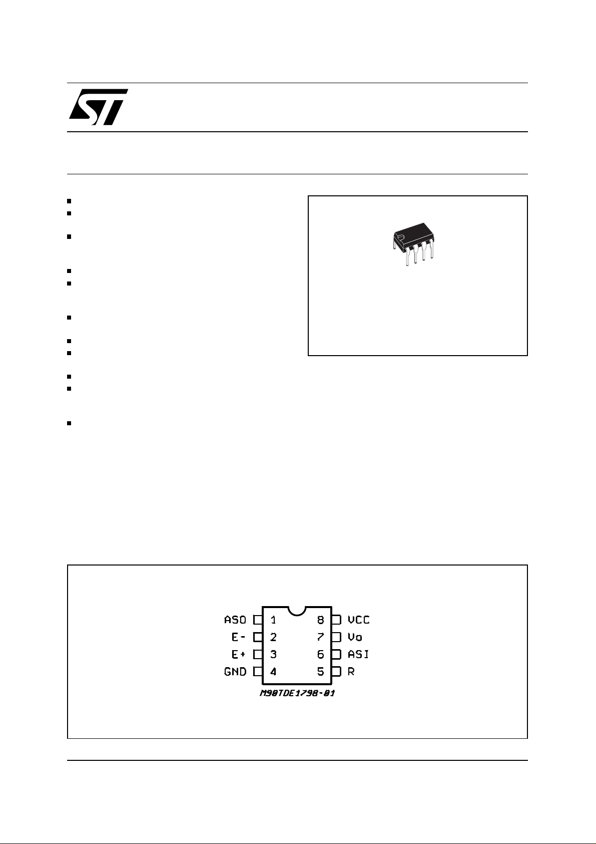
PIN CONNECTION (Top view)
September 2003
1/14
Page 2

TDE1798
ABSOLUTE MAXIMUM RATINGS
Symbol Parameter Test Conditions Unit
V
V
V
V
I(reset)
I
P
W
T
T
I
A(sink)
I
A(source)
Supply Voltage 50 V
CC
Input Differential Voltage 50 V
ID
Input Voltage -30 to +50 V
I
Reset Input Voltage VCC -50 to V
Output Current internally limited A
O
Power Dissipation Internally Limited mW
tot
Reset Input Sink Current (in thermal shut-down) 15 mA
Repetitive Maximum Demagnetization Energy - 106 Operations 150 mJ
D
Operating Ambient Temperature Range -25 to -85
op
Storage Temperature Range -65 to +150
stg
Alarm Output Sink Current 25 mA
Alarm Output Source Current 12 mA
CC
V
C
°
C
°
BLOCK DIAGRAM
2/14
Page 3

TDE1798
THERMAL DATA
Symbol Description Value Unit
R
th j-case
R
th j-ambient
1)
Devices bounded on a 40cm
Thermal Resistance Junction-case (1)
Thermal Resistance Junction-ambient (1)
2
glass-epoxy printed circuit 0.15cm thick with 4cm2 of copper
ELECTRICAL CHARACTERISTICS (note 2)
TDE -25°C ≤ T
Symbol Parameter Test Condition Min. Typ. Max. Unit
V
IO
I
CC
I
IB
V
ICR
V
I
I
SC
- VOOutput Saturation Voltage IO = 500mA (|V+ I - V- I|> 50mV) – 1 1.25 V
V
CC
I
OL
I
(pin 1) source
I
(pin 6) sink
I
RH
I
RL
V
th
I
reset
I
OL(open GND)
V
BRVEO
Notes:
2)
For operating at high temperature, the TDE1798 must be derated based on a 150°C maximum junction temperature and the junction-ambient
thermal resistance.
3)
The offset voltage given is the maximum value of input differential voltage required to drive the output voltage within 2V of the ground or the
supply voltage;
4)
Input voltage range is independent of the supply voltage;
5)
The reference input can be the inverting or the non-inverting one.
≤ +85°C, 6V ≤ VCC ≤ +35V, Io ≤ 500mA (unless otherwise specified).
j
Input Offset Voltage (note 3) – 2 50 mV
Power Supply Current Output High (Tamb = +25°C,
I
= 500mA)
o
Output Low
Input Bias Current – 15 40
Common-mod e I npu t V olt age
(note 4) 1 – 45 V
Range
Input Voltage Range V
> +1V, (note 4 and 5) -25 – 45 V
ref
Short-circuit Output Current VCC = 30V, t = 10ms 0.7 0.9 1.3 A
Output Low Leakage Current Tj = +85°C (VCC = 30V, VO = 0V) – 10 100
Available Alarm Output Current Source (V
= VCC - 2.5V)
(pin 1)
Sink (in thermal shut-down)
V
= 2V
(pin 6)
Reset Input Current –
Reset Threshold 0.8 1.4 2 V
Reset Output Sink Current (in thermal shut-down) for
V
≤ +0.8V
reset
Output Leakage Current (open ground) – 10 100
Output Transistor Avalanche Volt. VCC - V
O
max.
max.
–
–
6.5
2
30
90
C/W
°
C/W
°
8
4
mA
mA
µ
µ
4
6
-1
15
15
8
0
40
+1
–
–
mA
mA
µ
µ
2––mA
µ
65 – 110 V
A
A
A
A
A
3/14
Page 4

TDE1798
4/14
Page 5
TDE1798
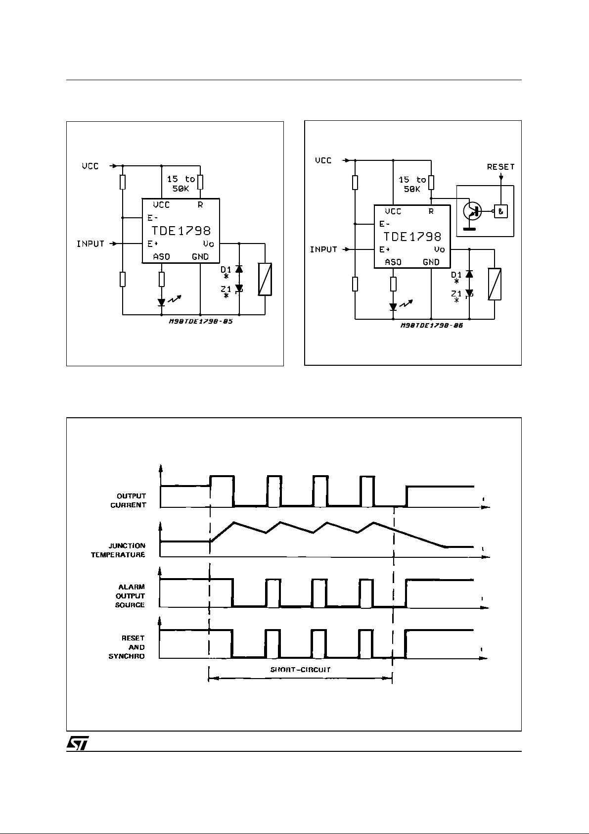
TYPICAL APPLICATION AUTOMATIC RESET
(*) D1 and Z1 needed if the demagnetization energy is higher than 150mJ
TYPICAL APPLICATION CONTROLLED RESET
SHORT CIRCUIT CONDITIONS WITH AUTOMATIC RESET
5/14
Page 6
TDE1798
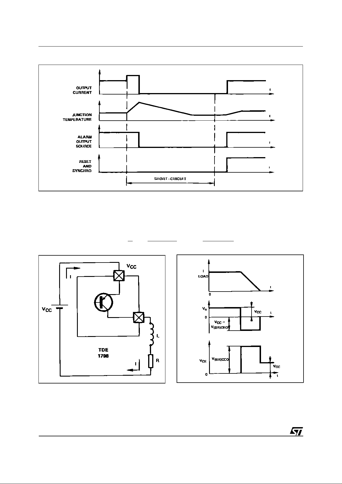
SHORT CIRCUIT CONDITIONS WITH CONTROLLED RESET
DEMAGNETIZATION OF INDUCTIVE LOADS
WITHOUT EXTERNAL CLAMPING DEVICES.
With no external clamping device, the energy of
demagnetization is dissipated in the TDE1798
output stage, an d the clam ping voltage is the col-
W = V
(BR)
L
R
[ Io −
V
(BR)
lector -emitter breakdown voltage V
This method provides a very fast demagnetization
of inductive loads and can be used up to 150 mJ.
The amount of energy W dissipated in the out put
stage during a demagnetization is :
− V
R
CC
Log ( 1 +
V
(BR)
V
CC
− V
) ]
CC
(BR)CEO
.
Remark 1 : This energy is dissipated inside the
case, then must be included in the whole power
dissipation.
Remark 2 : The use of external clamping device
is recommended in case of parallel driving of
6/14
loads. The dispersion of the collector-emitter
breakdown voltage V(BR) would induce the circuit
with the lowest V(BR) to dissipate t he whole demagnetization energy (which is roughly proportionnal to I
2
).
O
Page 7
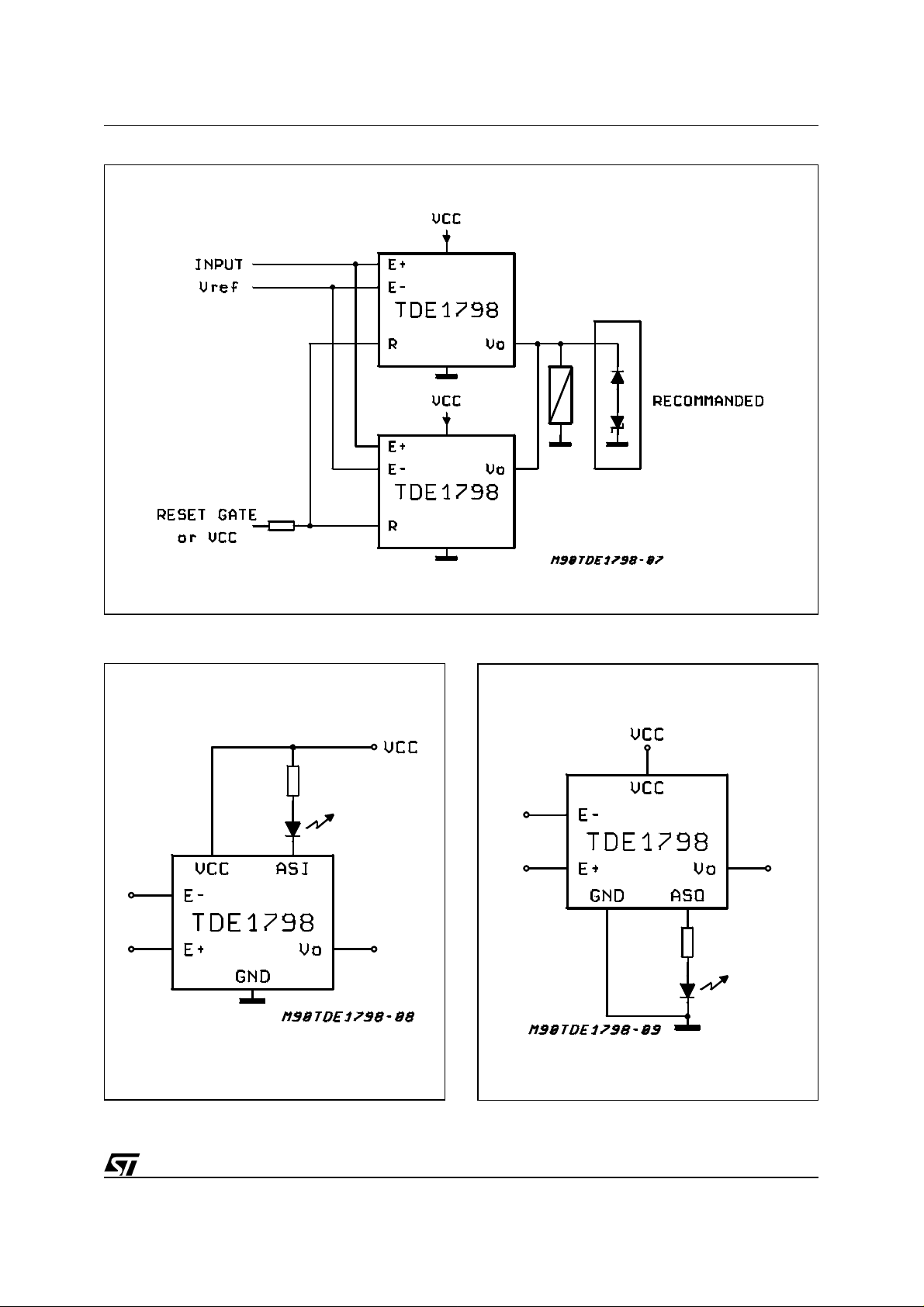
A 1 AMP. DRIVER (reset may be either automatic or controlled)
TDE1798
ALARM OUTPUT SINK ALARM OUTPUT SOURCE
7/14
Page 8
TDE1798
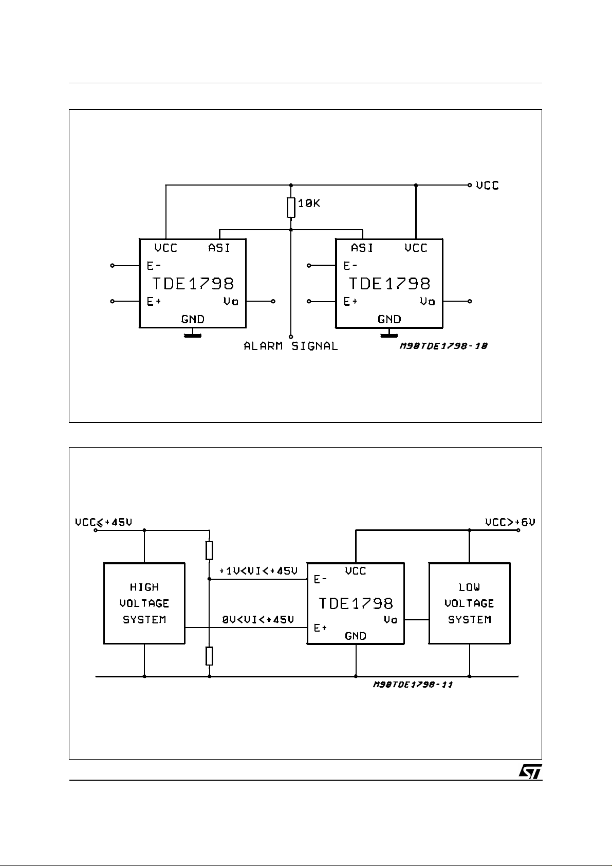
PARALLEL ALARM OUTPUTS
INTERFACE BETWEEN HIGH VOLTAGE AND LOW VOLTAGE SYSTEM
8/14
Page 9
TDE1798
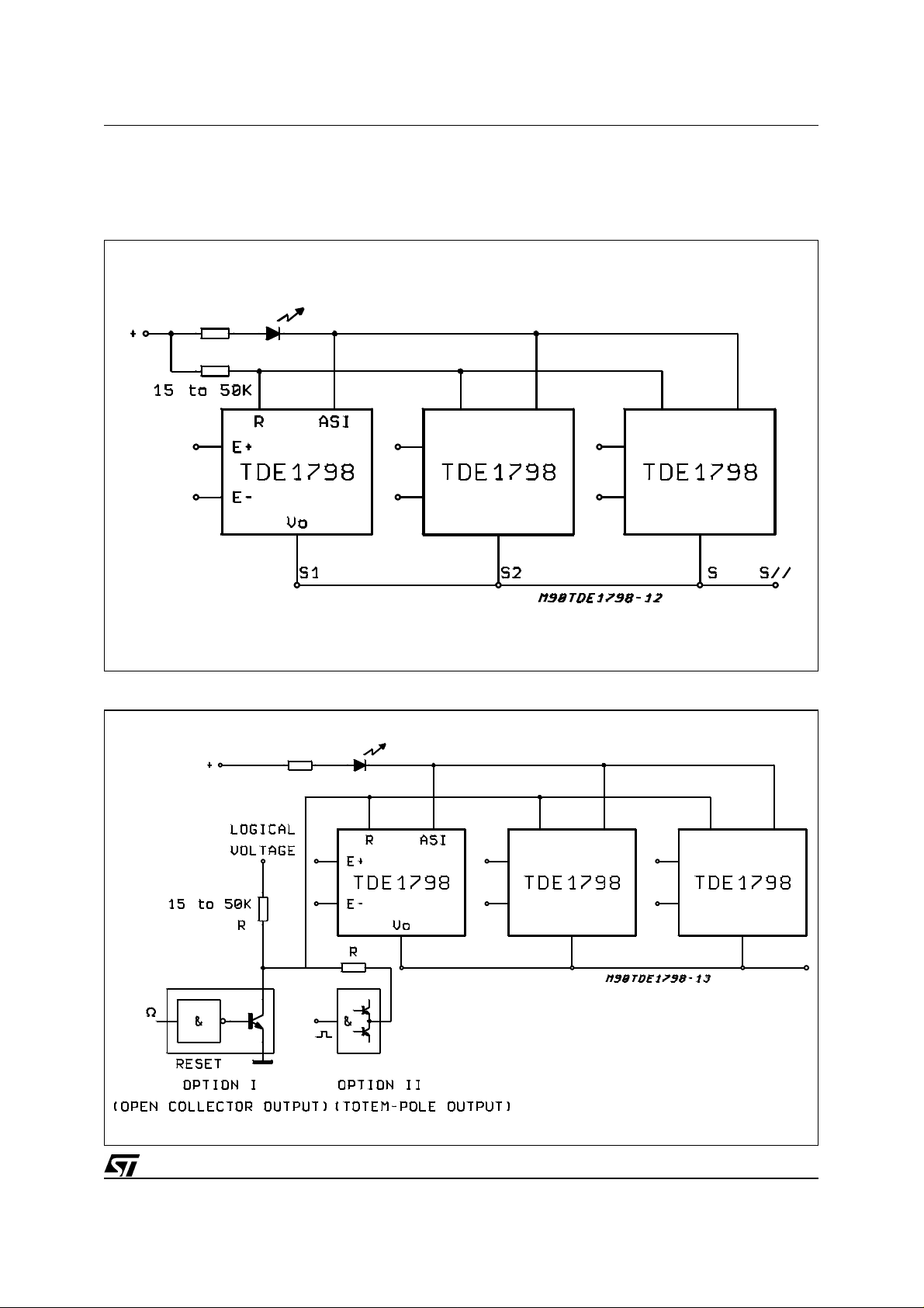
RESET AND SYNCHRONIZATION
Recommended diagram when the outputs are in
sible when all the circuits are returned in operating conditions.
parallel. After thermal disjunction a r estart is posSYNCRONOUS AUTOMATIC RESET (parallel or independent outputs)
SYNCHRONOUS CONTROLLED RESET (parallel or idependent outputs)
9/14
Page 10
TDE1798
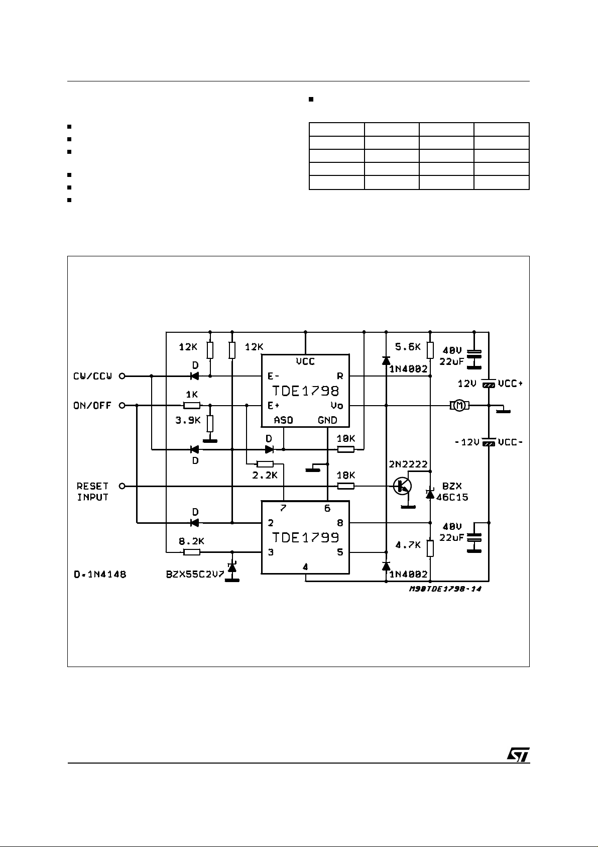
TWO QUADRANTS D.C. MOTOR DRIVE
MAIN FEATUR E S
VCC - VCC ≤ 50V
Maximum output current 0.5A
Full protection against overloads and short-cir-
cuits
No need of deadtime during rotation reversing
TTL compatible inputs
TDE1799 and TDE1798 input signals have the
same reference
No automatic restart after disjunction
CW/CCW ON PFF 1798 1799
0 0 OFF OFF
0 1 ON OFF
1 1 OFF ON
1 0 OFF OFF
10/14
Page 11
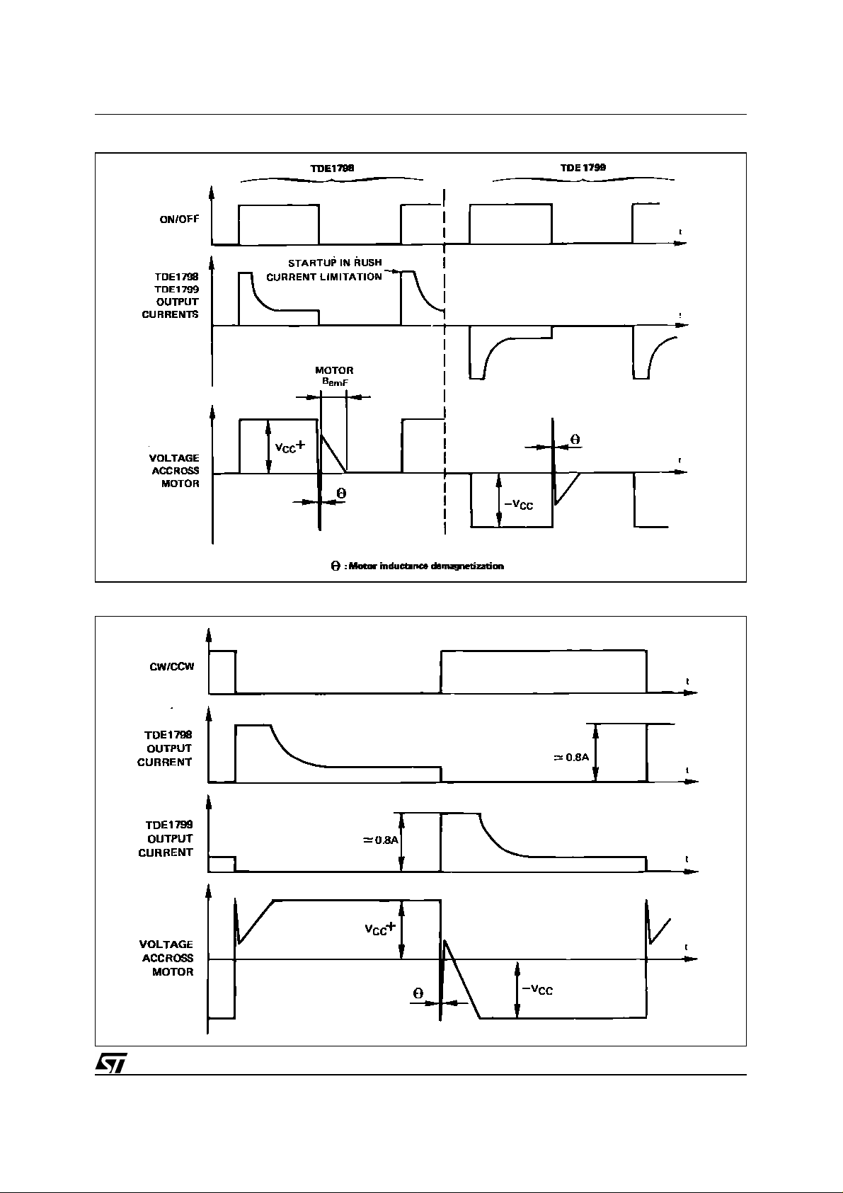
ON/OFF CYCLES
TDE1798
ROTATION REVERSING
11/14
Page 12
TDE1798
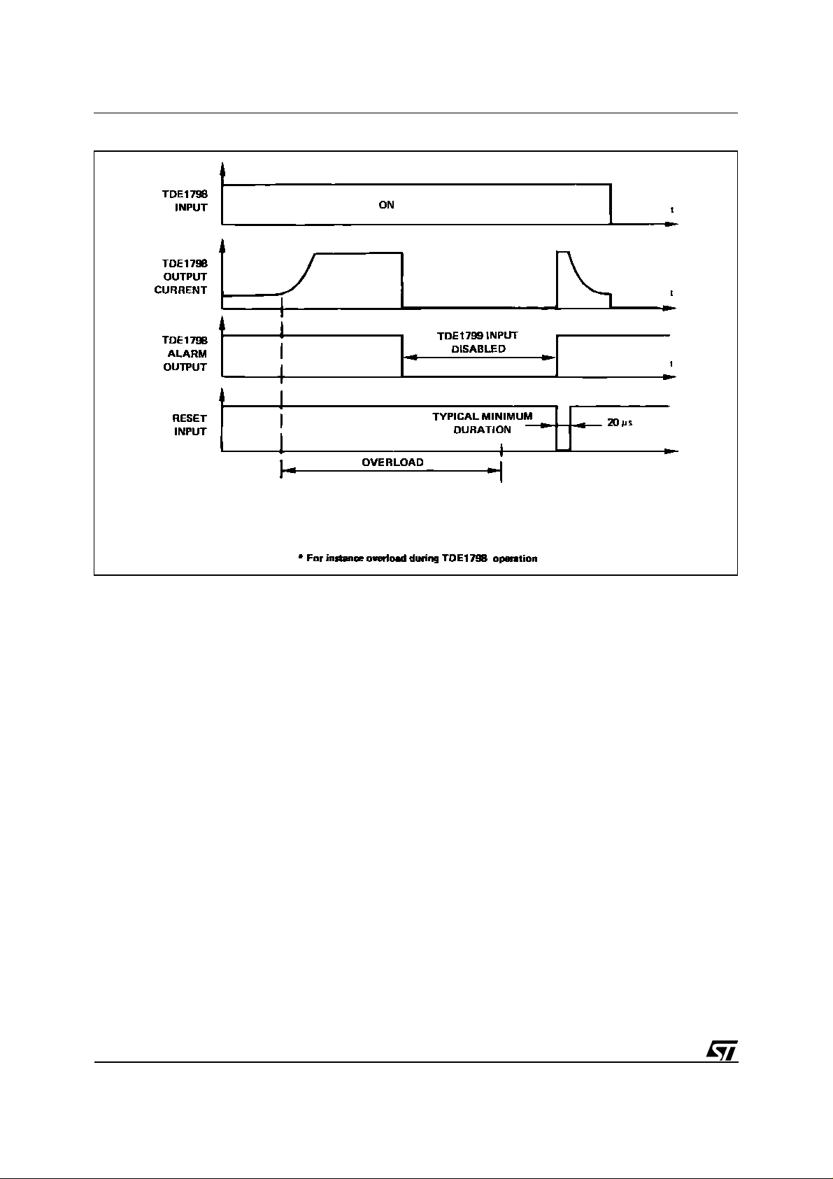
OVERLOAD CONDITIONS
12/14
Page 13
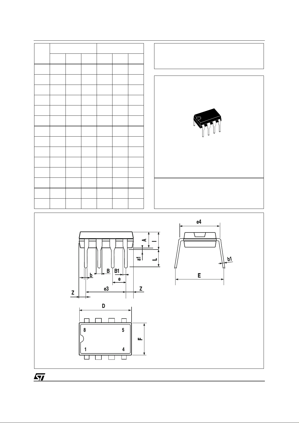
mm inch
DIM.
MIN. TYP. MAX. MIN. TYP. MAX.
A 3.32 0.131
a1 0.51 0.020
B 1.15 1.65 0.045 0.065
b 0.356 0.55 0.014 0.022
b1 0.204 0.304 0.008 0.012
D 10.92 0.430
E 7.95 9.75 0.313 0.384
e2.54 0.100
e3 7.62 0.300
e4 7.62 0.300
F 6.6 0.260
I 5.08 0.200
TDE1798
OUTLINE AND
MECHANICAL DATA
L 3.18 3.81 0.125 0.150
Z 1.52 0.060
Minidip
13/14
Page 14

TDE1798
Information furnishe d is beli eved to be accu rate and reliable. However, STMicroelec tronics assumes no res ponsibility for the consequences
of use of such i nformation nor for any i nfringement of patents or ot her rights of third par ties which may result from its use. No license i s
granted by imp lication or otherwi se under a ny patent or patent rights of STMicro electronics . Speci fications ment ioned in this publicat ion are
subject to change without notic e. This public ation supers edes and replaces all information prev iously supplied. STMic roelec tronic s products
are not authorized for use as critical components in life support devices or systems without express written approval of STMicroelectronics.
The ST logo is a registered trademark of STMicroelect roni cs.
All other names are the property of their respective owners
© 2003 STMicroelectronic s - All rights rese rved
STMicroelectronics GROUP OF COMPANIES
Australia – Belgium - Brazi l - Canada - China – Czec h Republ i c - Finland - France - Germany - Hong Kong - India - Israel - Italy - Ja pa n -
Malaysia - Malta - Morocco - Singapore - Spain - Sweden - Switzerland - United Kingdom - United States
www.st.com
14/14
 Loading...