

Page 1
Features
■ Low side or high side switch configuration
■ 6 V to 48 V supply voltage range
■ Overload and short circuit protections
■ Internal voltage clamping
■ Supply and output reversal protection
■ Thermal shutdown
■ GND and V
■ Adjustable delay at switch on
■ Indicator status led driver
■ +5 V regulated aux. voltage
■ High burst immunity
open wire protection
S
Description
The TDE1708DFT is an integrated power switch
with up to 48 V power supply capability. Two
output configurations are possible:
Load to GND (high side mode)
Load to V
Especially dedicated to proximity detectors, its
internal +5 V supply can be used to supply
external circuits (See also AN495).
(low side mode)
S
TDE1708DFT
Intelligent power switch
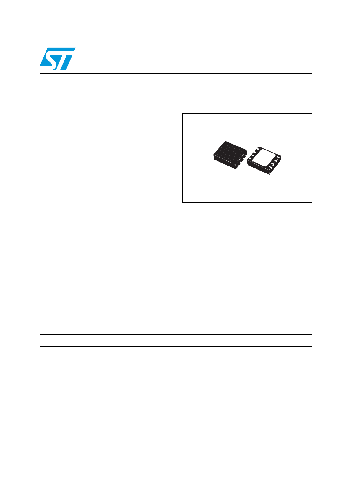
DFN (4x4)
A signal is internally generated to block the In
signal, and prevent activation of the output switch,
as long as an abnormal condition is detected. The
power-on transition, as well as the chip over
temperature and the output overcurrent, concur to
the generation of such signal. A minimum delay of
25 ms (Typ. value) is added to the trailing edge of
such signal to ensure that a stable normal
situation is present when the signal disappears.
The delay (of the disappearance of the block
signal; no delay at its on set) can be further
increased connecting a capacitor between pin3
and ground. It can drive resistive or inductive
loads.
Table 1. Device summary
Order code Temp. range, °CPackage Packing
TDE1708DFT -25 °C to +85 °C DFN (4x4) Tape and reel
February 2009 Rev 4 1/14
www.st.com
14
Page 2

Contents TDE1708DFT
Contents
1 Block and pin connection diagrams . . . . . . . . . . . . . . . . . . . . . . . . . . . . 3
2 Electrical specifications . . . . . . . . . . . . . . . . . . . . . . . . . . . . . . . . . . . . . . 5
2.1 Thermal data . . . . . . . . . . . . . . . . . . . . . . . . . . . . . . . . . . . . . . . . . . . . . . . 5
2.2 Absolute maximum ratings . . . . . . . . . . . . . . . . . . . . . . . . . . . . . . . . . . . . . 5
2.3 Electrical characteristics . . . . . . . . . . . . . . . . . . . . . . . . . . . . . . . . . . . . . . . 6
2.4 Dynamic information . . . . . . . . . . . . . . . . . . . . . . . . . . . . . . . . . . . . . . . . . . 7
3 Application information . . . . . . . . . . . . . . . . . . . . . . . . . . . . . . . . . . . . . . 8
3.1 Adjustable input hysteresis circuit . . . . . . . . . . . . . . . . . . . . . . . . . . . . . . . 9
4 Package mechanical data . . . . . . . . . . . . . . . . . . . . . . . . . . . . . . . . . . . . 10
4.1 Foot print recommended . . . . . . . . . . . . . . . . . . . . . . . . . . . . . . . . . . . . . 10
4.2 DFN (4x4) mechanical data and package dimensions . . . . . . . . . . . . . . . 11
5 Revision history . . . . . . . . . . . . . . . . . . . . . . . . . . . . . . . . . . . . . . . . . . . 13
2/14
Page 3
TDE1708DFT Block and pin connection diagrams
1 Block and pin connection diagrams
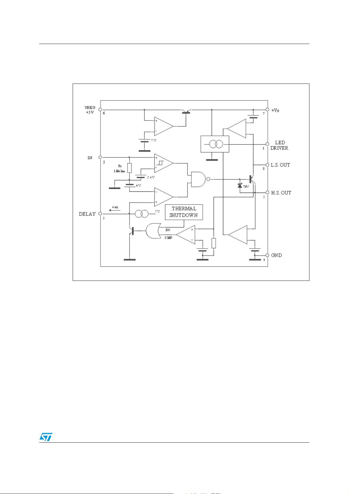
Figure 1. Block diagram
3/14
Page 4
Block and pin connection diagrams TDE1708DFT
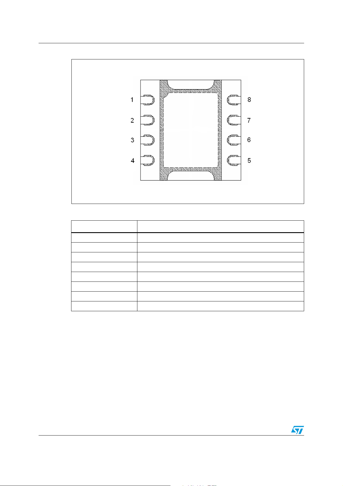
Figure 2. Pin connection diagram (top view)
Table 2. Pin functions
o
Pin N
1 Led driver
2 High side output
3 Delay capacitance source
4Ground
5 Input
6 Reg. voltage source
7 Supply voltage
8 Low side output
Note: Lead frame can be connected to ground.
Function
4/14
Page 5
TDE1708DFT Electrical specifications
2 Electrical specifications
2.1 Thermal data
Table 3. Thermal data
Symbol Description Value Unit
R
thJA
R
thJC
1. Soldered to a 4 layer board with 4 vias in the pad.
Thermal resistance junction-ambient. (max) 32
Thermal resistance junction-case. (max) 1.2 °C/W
2.2 Absolute maximum ratings
Table 4. Absolute maximum ratings
Symbol Parameter Value Unit
(1)
°C/W
Supply voltage 50 V
S
Supply reverse voltage 50 V
S
Output current internally limited A
Regulated voltage pin 0 to 7 V
Delay cap. source pin 0 to 5 V
Output dif. voltage 55 V
o
Input voltage -10 to 50 V
i
Junction operating temperature Internally limited °C
J
Storage temperature range -55 to 150 °C
Power dissipation internally limited mW
Energy inductive load 100 mJ
i
V
V
V
I
V
reg
delay
V
V
T
T
stg
P
E
o
tot
5/14
Page 6
Electrical specifications TDE1708DFT
2.3 Electrical characteristics
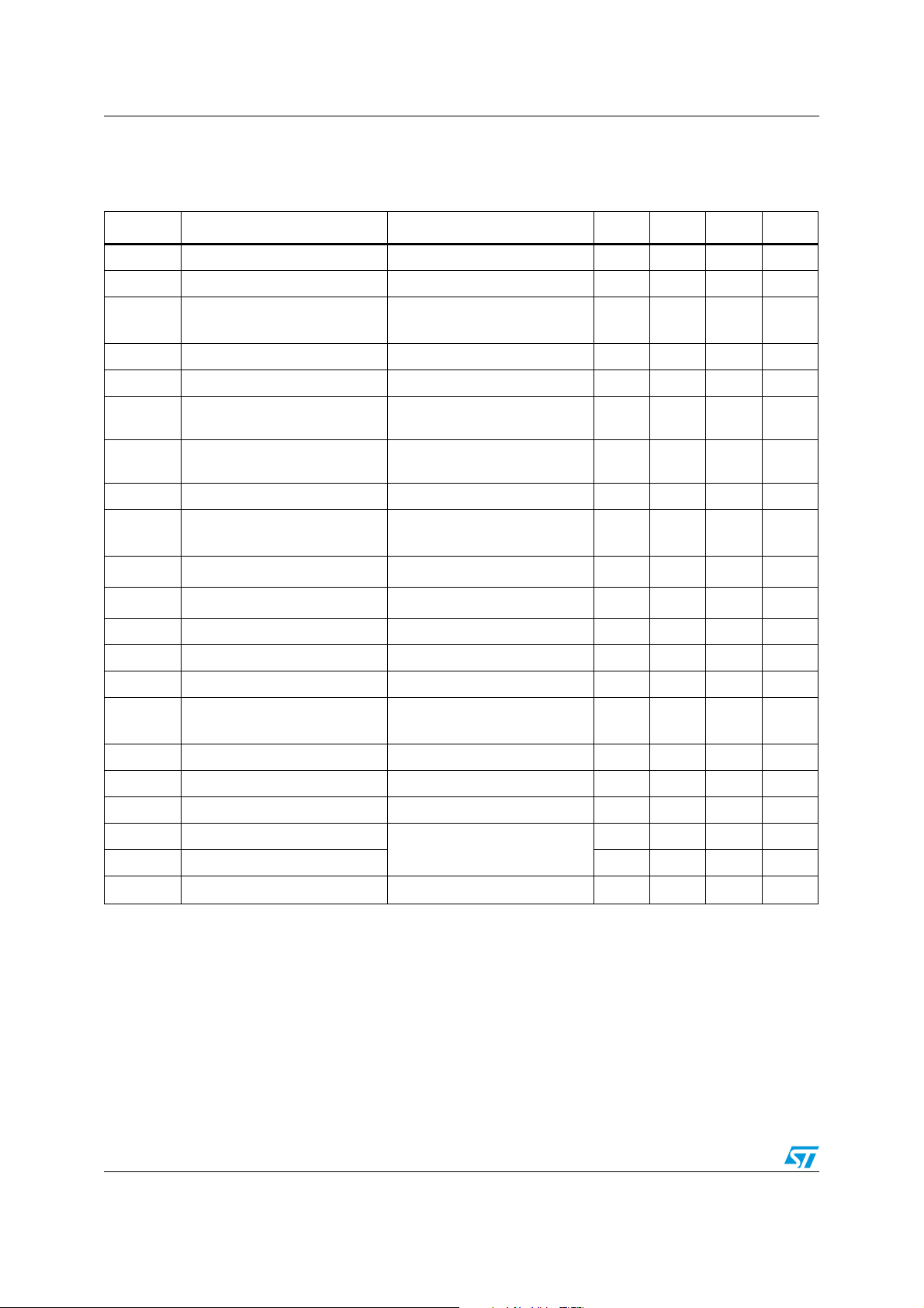
Table 5. Electrical characteristics
(V
= 24 V; TJ = - 25 to +85 °C unless otherwise specified)
S
Symbol Parameter Test conditions Min Typ Max Unit
V
I
I
I
V
I
SCLS
I
SCHS
V
I
olk
V
V
I
V
I
scr
I
reg
I
old
V
Supply voltage 6 48 V
s
Supply reverse current VSR = –48 V 1.5 mA
sr
Quiescent current
q
Output current Vs = 6 to 48 V 250 mA
o
Output voltage drop Io = 200 mA 1 1.5 V
sat
Short circuit current in low side
configuration
Short circuit current in high side
configuration
Internal voltage clamp ICL = 10 mA 55 70 V
cl
Output leakage
Input voltage threshold 2 3 V
ith
Input threshold hysteresis 300 mV
ihis
Input current Vi = 5 V 2 5 μA
lk
Regulated output voltage I
reg
Short circuit regulated 6 30 50 mA
Output regulator current
Current source sink led driver Output ON (±)234mA
Voltage drop led driver Ios = 2 mA (±) 1.2 1.6 V
old
Oldlk LED driver (off) Leak. V
Del. cap. charge current
Delay voltage trigger 4 V
dth
Thermal shutdown temperature 180 °C
T
I
dch
V
TSD
I
= I
reg
V
= 0; Vi < 2 V;
led
= 6 to 48 V
S
1.5 mA
0.3 0.4 0.6 A
0.25 0.3 0.40 A
(Pin 2)
Vi < 2 V; Vo = 0 to Vs (Pin 8)
< 5 mA 4.5 5 5.5 V
reg
V
= 35 V
s
= 48 V
V
s
< 2 V; RL < 1 kΩ 10 μA
i
100
300
100
6
4
246μA
= 25 °C
T
J
μA
μA
mA
mA
6/14
Page 7

TDE1708DFT Electrical specifications
2.4 Dynamic information
Table 6. Dynamic information (VS = 24 V; TJ = 25 °C; RL = 48 Ω)
Symbol Parameter Test conditions Min Typ Max Unit
t
on
t
off
t
don
t
d min
Propagation turn on time Vi = 0 to 5V 15 μs
Propagation turn off time 15 μs
Delayed turn on time / nF
delay capacitor
Minimum delayed t
on
Delay capacitor = 0
0.65 1 2 ms
25 μs
7/14
Page 8
Application information TDE1708DFT
3 Application information
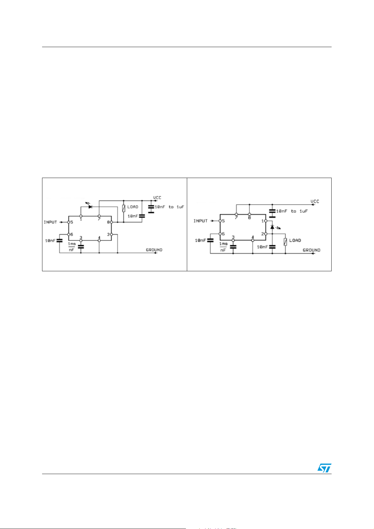
The LED driver tells the output status. It can source or sink current (I
old typ
= 3 mA),
according to the output configuration chosen. The thresholds, represented by the output
comparator in the block diagram, are set at about 1.5 V - 2 V.
For instance, in the high side load case of the Application Circuit, when the voltage on pin 8
(the output) differs from V
less than 1.5 V, the output is sensed in “OFF” state and the
CC
LED driver is disabled.
If instead pin 8 differs from V
more than 3 V (the output comparator threshold value plus
CC
the drop voltage on the LED), then the output is sensed “ON” and the driver will force the
current on the LED.
Figure 3. Low side driver topology Figure 4. High side driver topology
TDE1708DFT
TDE1708DFTDE1708DFT
8/14
Page 9
TDE1708DFT Application information
3.1 Adjustable input hysteresis circuit
The TDE1708DFT is a device realized in bipolar technology and therefore it has the usual
problems of temperature compensation that such technology involves; despite all it
maintains an input dynamics within 1 V over industrial temperatures range.
In all input voltage range it will guarantee a high impedance of 1 MΩ determining an input
current about 2 µA.
Exploiting this input high impedance is possible connects a sensor directly on it and bypass
the obstacle of active signal conditioning circuit using a voltage firm point as ground of
sensor, the delay capacitor, connected on the pin 3, as low pass filter and capacitor on Vreg
pin to minimize the noise on it and protect for errors the low-voltage internal circuits,
according AN495.
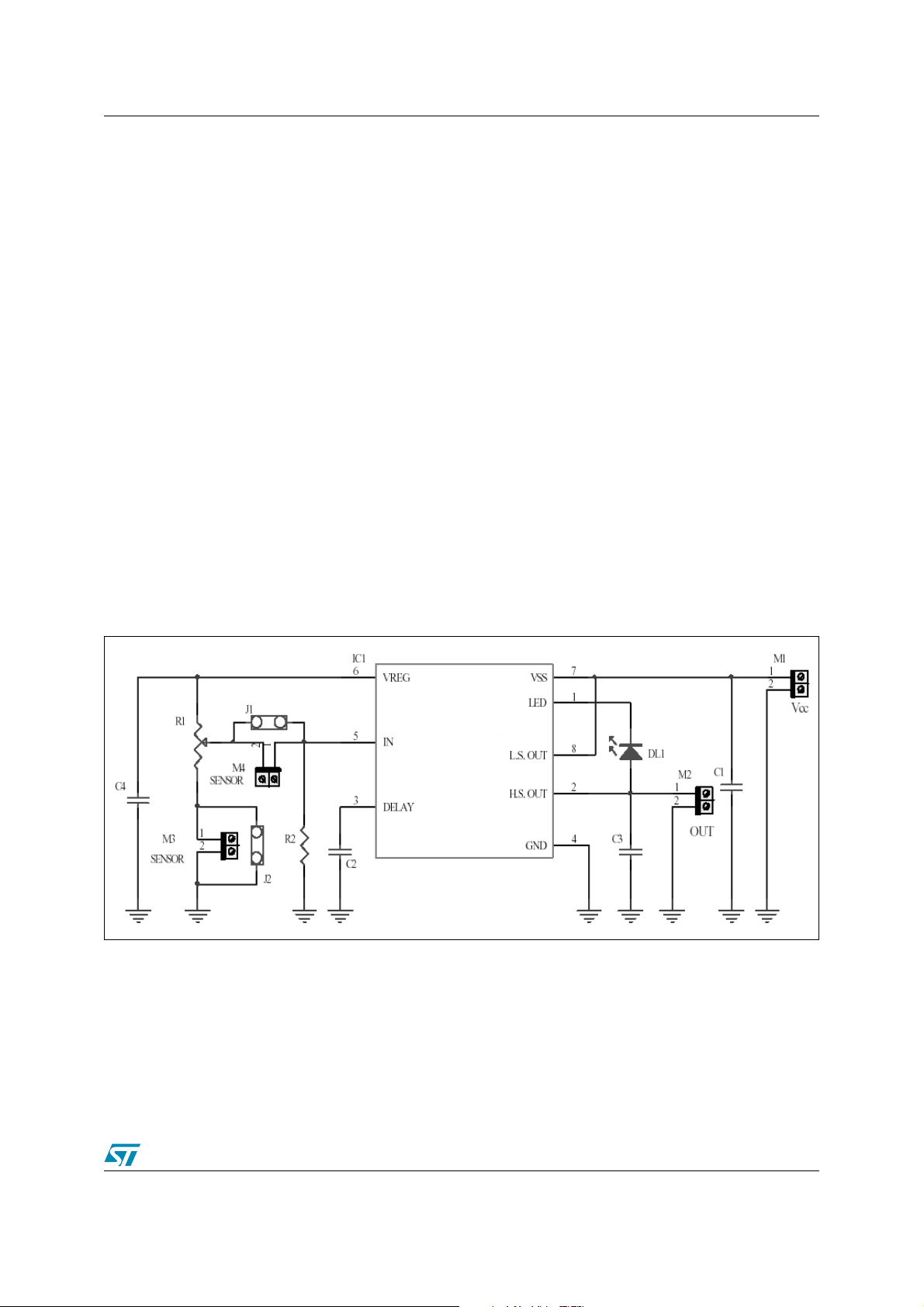
In Figure 5. the input external network is optimized for accepting both a sensor with ground
connected to the body and a sensor with independent ground.
In order to ground the body of the sensor, J1 has to be shorted, while J2 opened and
connect the sensor on M3; in case of independent ground J1 must be opened, J2 shorted
and the sensor connected on M4.
DL1 indicate commutation status of the device output and C3 realize a simple output filtering
in case is used an inductive load. With C2 about 10 nF we obtain a good filtering and
immunity from input voltage noise. C4 is 4,7nF according AN495.
R2 is an optional resistor plugged only when the sensor needs to adapt its impedance with
the input impedance of device.
Figure 5. Application circuit for adjustable input hysteresis
TDE1708DFT
9/14
Page 10
Package mechanical data TDE1708DFT
4 Package mechanical data
In order to meet environmental requirements, ST offers these devices in different grades of
ECOPACK
®
packages, depending on their level of environmental compliance. ECOPACK®
specifications, grade definitions and product status are available at: www.st.com. ECOPACK
is an ST trademark.
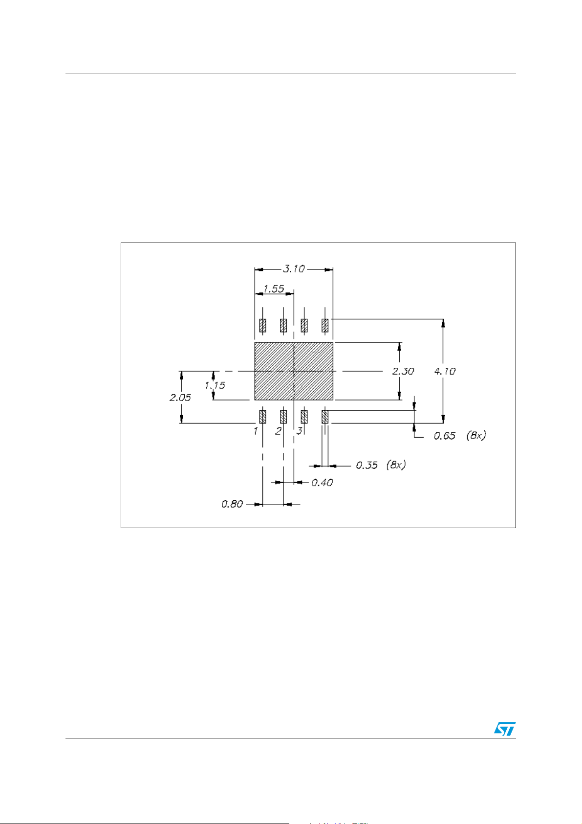
4.1 Foot print recommended
Figure 6. Foot print
10/14
Page 11
TDE1708DFT Package mechanical data
4.2 DFN (4x4) mechanical data and package dimensions
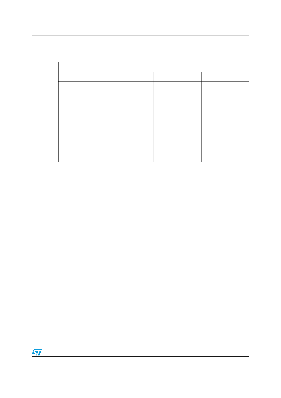
Table 7. Package dimensions
mm
Dim.
Typ Mi n Ma x
A 0.90 0.80 1
A1 0.02 0 0.05
A3 0.20
b 0.30 0.23 0.38
D 4 3.90 4.10
D2 3 2.82 3.23
E 4 3.90 4.10
E2 2.20 2.30
e0.80
L 0.50 0.40 0.60
11/14
Page 12
Package mechanical data TDE1708DFT
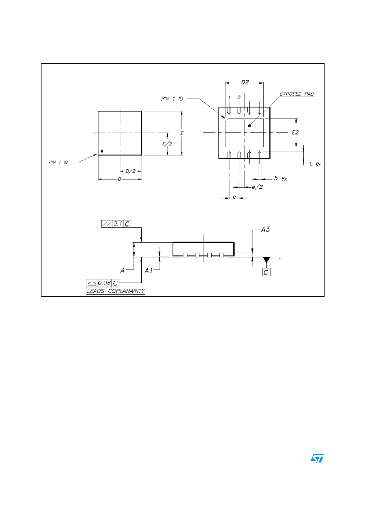
Figure 7. Package dimension
Sitting plane
Bottom viewTo p vi ew
12/14
Page 13
TDE1708DFT Revision history
5 Revision history
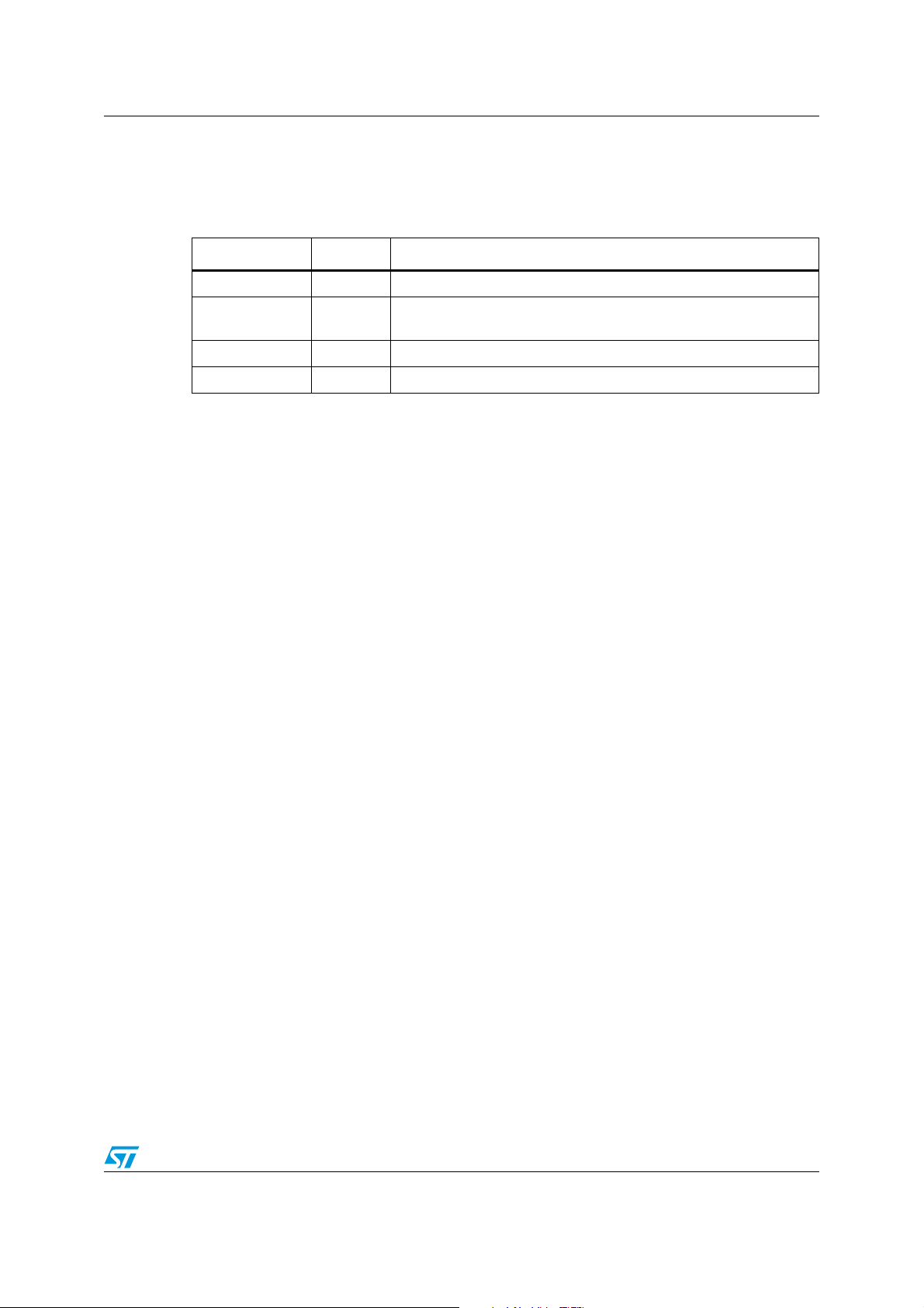
Figure 8. Document revision history
Date Revision Changes
26-Jun-2006 1 Initial release.
31-Oct-2006 2
Updated package in cover page, inserted low/high side I
5.
in Ta b le
SC
09-Jan-2007 3 Updated I
27-Feb-2009 4 Updated cover page
in Table 5 on page 6.
SCHS
13/14
Page 14

TDE1708DFT
Please Read Carefully:
Information in this document is provided solely in connection with ST products. STMicroelectronics NV and its subsidiaries (“ST”) reserve the
right to make changes, corrections, modifications or improvements, to this document, and the products and services described herein at any
time, without notice.
All ST products are sold pursuant to ST’s terms and conditions of sale.
Purchasers are solely responsible for the choice, selection and use of the ST products and services described herein, and ST assumes no
liability whatsoever relating to the choice, selection or use of the ST products and services described herein.
No license, express or implied, by estoppel or otherwise, to any intellectual property rights is granted under this document. If any part of this
document refers to any third party products or services it shall not be deemed a license grant by ST for the use of such third party products
or services, or any intellectual property contained therein or considered as a warranty covering the use in any manner whatsoever of such
third party products or services or any intellectual property contained therein.
UNLESS OTHERWISE SET FORTH IN ST’S TERMS AND CONDITIONS OF SALE ST DISCLAIMS ANY EXPRESS OR IMPLIED
WARRANTY WITH RESPECT TO THE USE AND/OR SALE OF ST PRODUCTS INCLUDING WITHOUT LIMITATION IMPLIED
WARRANTIES OF MERCHANTABILITY, FITNESS FOR A PARTICULAR PURPOSE (AND THEIR EQUIVALENTS UNDER THE LAWS
OF ANY JURISDICTION), OR INFRINGEMENT OF ANY PATENT, COPYRIGHT OR OTHER INTELLECTUAL PROPERTY RIGHT.
UNLESS EXPRESSLY APPROVED IN WRITING BY AN AUTHORIZED ST REPRESENTATIVE, ST PRODUCTS ARE NOT
RECOMMENDED, AUTHORIZED OR WARRANTED FOR USE IN MILITARY, AIR CRAFT, SPACE, LIFE SAVING, OR LIFE SUSTAINING
APPLICATIONS, NOR IN PRODUCTS OR SYSTEMS WHERE FAILURE OR MALFUNCTION MAY RESULT IN PERSONAL INJURY,
DEATH, OR SEVERE PROPERTY OR ENVIRONMENTAL DAMAGE. ST PRODUCTS WHICH ARE NOT SPECIFIED AS "AUTOMOTIVE
GRADE" MAY ONLY BE USED IN AUTOMOTIVE APPLICATIONS AT USER’S OWN RISK.
Resale of ST products with provisions different from the statements and/or technical features set forth in this document shall immediately void
any warranty granted by ST for the ST product or service described herein and shall not create or extend in any manner whatsoever, any
liability of ST.
ST and the ST logo are trademarks or registered trademarks of ST in various countries.
Information in this document supersedes and replaces all information previously supplied.
The ST logo is a registered trademark of STMicroelectronics. All other names are the property of their respective owners.
© 2009 STMicroelectronics - All rights reserved
STMicroelectronics group of companies
Australia - Belgium - Brazil - Canada - China - Czech Republic - Finland - France - Germany - Hong Kong - India - Israel - Italy - Japan -
Malaysia - Malta - Morocco - Singapore - Spain - Sweden - Switzerland - United Kingdom - United States of America
www.st.com
14/14
 Loading...