

4-HEAD VIDEOAND 2-HEADSHIFI AUDIO
PLAYBACKAND RECORD AMPLIFIERFORVCR
.
ONE 5V POWERSUPPLY
.
PLAYBACK/RECORD MODE SELECTION
THROUGH A LOGICINPUT
.
PINNING COMPATIBLE WITH STV5725 AND
STV5727
.
SO28 PACKAGE
PLAYBACK MODE
.
LOW NOISE AND WIDE BAND AMPLIFIERS
FOR4 VIDEOHEADS
.
AUTOMATIC OFFSET CANCELLATION
BETWEENTHE 2 SELECTEDHEADS
.
ONE PLAYBACKOUTPUT WITH AGC
.
ONE PLAYBACKOUTPUT(60dB CONSTANT
GAIN)
.
ONE OUTPUT FOR AUTOMATIC VIDEO
TRACKING
.
SP/LPENVELOPECOMPARATOROUTPUT
.
LOWNOISEAMPLIFIERSFOR 2 HIFIHEADS
.
HIFI OUTPUT GAIN (70dB)
RECORDMODE
.
TRANSCONDUCTANCE AMPLIFIER FOR
VIDEO
.
AGC AMPLIFIER FORHIFI
DESCRIPTION
STV5728is intendedfor4 headsVCR applications
withHIFI.It includesall the electricalfunctionsnecessaryto achieveplay-backandrecordprocessing.
Recordor PlaybackModecanbe selectedthrough
SWR Pin. SWH allows to select the video head
input(H1SPor H2SP,H1LP or H2LP), whileSWM
will select the mode SP or LP. The SWFMH will
selecttheFMinputheadsin Playbackandwillmute
the HIFI record amplifier in Record Mode.
PlaybackMode (Video)
Signalsapplied on H1SP, H2SP, H1LP and H2LP
input pins will be amplified by 60dB voltage gain.
I
ground. The input signal can be selected through
SWHand SWM inputs and the corresponding output signal will be availableon PinCPB. The offset
OUTSP
and I
Pins are AC short-circuited to
OUTLP
STV5728
voltage between the two selected heads is automaticallycancelledafter 32 switchinghead cycles.
A constant output signal will be available on Pin
YPB thanks to an AGC function (Automatic Gain
Control). The time constant of the AGC is determined by the capacitorvalue connected to CAGC
Pin. For Automatic Tracking, a signal which is a
function of the selected input signal amplitude is
present on Pin TRIV. For Trick Mode, a signal
resulting from the comparison of the input signal
amplitudeis availableon ENVC Pin.
SO28
(Plastic Package)
ORDER CODE : STV5728
PIN CONNECTIONS
H1SP
GNDSP
H2SP
I
OUTSP
CCOM
I
OUTLP
H2LP
GNDLP
H1LP
CCOM2
I
OUTFM
H1FM
GNDFM
H2FM
1
2
3
4
5
6
7
8
9
10
11
12
13
14
28
27
26
25
24
23
22
21
20
19
18
17
16
15
SWR
SWIN
V
CC
RECIN
CPB
GND
YPB
TRIV
ENV
CAGC
FMRIN
FMPB
SWFMH
V
CCFM
5728-01.EPS
May 1997
1/11
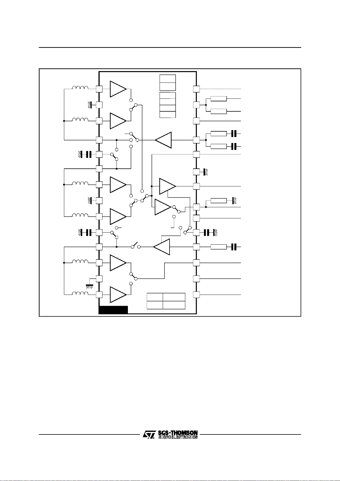
STV5728
BLOCKDIAGRAM
H1SP
H2SP
SP HEADS
CCOM
LP HEADS
H2LP
H1LP
CCOM2
HIFIHEADS
H1FM
60dB
1
2
3
60dB
4
5
6
60dB
7
8
60dB
9
10 19
11
12
Detector
Record Reference
70dB
Current (FM)
Record AGC
REC
PB
H2LP
H1LP
H1SP
H2SP
Record
Amplificator
Playback
AGC
28
27
26
25
24
23
22
21
20
18
17
+5V
CAGC
22k
8.2k
Rrcy
Rrcc
R
ADJ
Rfmin
Ω
Ω
SWR
SWH
SWM
V
CC
YREC
CREC
CPB
YPB
TRIV(ATR)
ENV
Envelope Comp
FMREC
FMPB
13
PB REC MUTE
H2FM
14
70dB
H1FM OFF
H2FM ON
STV5728
FUNCTIONAL DESCRIPTION
RecordMode (Video)
ThecurrentinputappliedonRECINPinis amplified
througha transconductanceamplifier.Specialcare
has been taken to speed up commutation from
Playbackto Record and fromRecordto Playback,
avoidingspikesthroughtheloads (the rotarytransformers).The recordingcurrentlevel inLP mode is
0.9 time the valueof SP one.
PlaybackMode (FM HIFI)
Signalsappliedon H1FMand H2FMinput Pinswill
be amplified by 70dB voltage gain. I
2/11
OUTFM
Pin is
16
15
+5V
SWFMH
V
CCFM
AC short-circuitedto groundbyCCOM1. The input
signal can be selected throughSWFMH input and
thecorrespondingoutput signalwill beavailableon
Pin FMPB.
Record Mode (HIFI)
ThecurrentinputappliedonFMRINPinis amplified
through an Automatic Gain Control amplifier. The
recordinglevelcan be adjustedthanks to the R
ADJ
resistanceconnectedtoTRIVPin.Specialcarehas
beentakento speedupcommutationfromPlayback
to Recordand from Record to Playback, avoiding
spikesthroughthe loads (therotarytransformers).
5728-02.EPS
STV5728
ABSOLUTEMAXIMUM RATINGS
Symbol Parameter Value Unit
V
CC
T
T
oper
THERMAL DATA
Symbol Parameter Value Unit
R
th (j-a)
RECOMMENDED OPERATING CHARACTERISTICS
Symbol Parameter Min. Typ. Max. Unit
V
CC
V
CCFM
CAGC AGC Time Constant 4.7 22 nF
CCOM Decoupling Capacitor 4.7 470 nF
CCOM1 Decoupling Capacitor 4.7 470 nF
R
ADJ
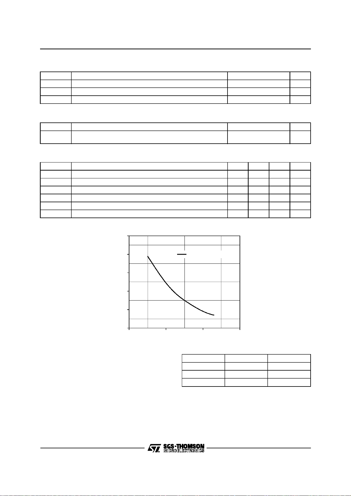
Figure 1 : FM RecordCurrentAmplifier; RecordCurrent Adjustment Curve
Power Supply Voltage 6 V
Junction Temperature 150
j
Operating Temperature 0, +70
Junction-ambient Thermal Resistance
Max. 75
(IC solded on the PC board)
Power Supply 4.75 5 5.25 V
FM HIFI Power Supply 4.75 5 5.25 V
Record Current Adjustment Resistor 15 22 33 k
70
o
C/W
o
C
o
C
5728-01.TBL
5728-02.TBL
Ω
5728-03.TBL
60
)
PP
50
40
Current(mA
30
20
10 20 30 40
A certain ratio must be kept between R
to insure maximum performances with an
R
FMIN
ADJ
and
averag e FM recording input voltage around
170mV
. Some examplesare given in the follow-
PP
ingtables.If theaverageinput voltage is higher (or
lower), the R
value must be increased (de-
FMRIN
creased)proportionnaly.
R
ADJ
RecordingLevel
Value(kΩ)
SET-UP R
(1) 15k
(2) 22kΩ 1.5kΩ
(3) 33kΩ 2kΩ
ADJ
5728-03.EPS
R
FMRIN
Ω
1k
Ω
3/11
STV5728
ELECTRICALCHARACTERISTICS (T
=25oC, unless otherwisespecified)
amb
PlaybackMode
= 5V,no loadon YPBand CPBPins, R
V
CC
Symbol Parameter Test Conditions Min. Typ. Max. Unit
PLAYBACK AMPLIFIER
I
CC1
Supply Current 40 48 53 mA
GPB Playback Gain Sinewave 600kHz, 0.4mV
EN Equivalent Voltage Noise
IN Equivalent Input Current Input open @ 6MHz, BW = 10kHz 1.4 2 2.6
CRT1 Crosstalk Between SP Channels
(or LP Channels)
CRT2 Crosstalk Sinewave @ 600kHz, 0.4mV
CRT3
Crosstalk Between SP1and LP2
Channels (or SP2 to LP1 Channels)
RPBSW Playback Switch on Resistor @ 6MHz 0.8 2.5 18
BWLCF Attenuation @ 100kHz Reference level @ 600kHz -1 0 1 dB
BWHCF Attenuation @ 8MHz Reference level @ 4MHz -3 1 0 dB
C
R
Input Capacitance @ 6MHz 22 27 32 pF
IN
Input Resistance @ 6MHz 500 730 950 Ω
IN
ZCPB Output Resistance DC 5 14 50
VDCPB1 DC Levelon Pin CPB 1.35 1.75 2.15 V
DVDC Head Switch Offset -200 0 200 mV
SHPB1 2nd Harmonic Sinuswave @ 4MHz, 0.4mV
PLAYBACK AGC FUNCTION
ZYPB Output Impedance @ YPB 5 14 50 Ω
VDCPB2 DC Level@ YPB 1.15 1.45 1.85 V
BWLCF2 Attenuation @ 100kHz Reference @ 4MHz, PB AGC locked -1 0 1 dB
BWHCF2 Attenuation @ 8MHz Reference @ 4MHz, PB AGC locked -3 -1 1 dB
VLPB Output Amplitude Sinuswave @ 4MHz, 0.4mV
SHPB2 Second Harmonic Sinuswave @ 4MHz, 0.4mVPPon input -44 -40 dB
IPB+ CAGC Sink Current 50 100 150
IPB- CAGC Source Current -150 -100 -50
DVLP AGC Sensitivity
TRIV FUNCTION
VTRIV0 Output Level (1) SP mode, V
VTRIV4 Output Level (4) LP mode, V
VTRIV5 Output Level (5) SP mode, V
VTRIV6 Output Level (6) SP mode, V
VTRIV7 Output Level (7) LP mode, V
VTRIV8 Output Level (8) LP mode, V
VTRIV9 Output Level (9) SP mode, V
VTRIV10 Output Level (10) SP mode, V
FTRIV1
FTRIV2
Response Lower Frequency,
Attenuation @ 1MHz
Response Higher Frequency,
Attenuation @ 8MHz
=22kΩ, after 32 SWH (SWitching Head) cycles.
ADJ
on inputs 58 60 62 dB
PP
Input grounded via I
BW = 10kHz
Sinewave @ 4MHz, 0.4mV
Sinewave @ 6MHz, 0.4mV
Sinuswave @ 4MHz, 0.2mV
-5dB and +6dB
= 0mVPP@ 4MHz 0.05 0.28 0.7 V
cpb
= 600mVPP@ 4MHz 4.1 V
cpb
= 100mVPP@ 4MHz 1.33 V
cpb
= 200mVPP@ 4MHz 2.27 V
cpb
= 100mVPP@ 4MHz 1.4 1.8 2.2 V
cpb
= 200mVPP@ 4MHz 3.11 V
cpb
= 300mVPP@ 4MHz 2.95 V
cpb
= 600mVPP@ 4MHz 3.85 V
cpb
Reference : SP mode, V
@ 4MHz
Reference : SP mode, V
@ 4MHz
Pin @ 600kHz,
OUT
PP
PP
PP
PP
PP
= 100mV
cpb
= 100mV
cpb
0.5 0.6 0.7
PP
on input 160 200 250 mV
on input,
PP
PP
-1 0 1 dB
-41 -39 dB
-50 dB
-60 -50 dB
-43 -37 dB
-6 dB
-1 dB
nV
√Hz
pA
Hz
√
Ω
Ω
µ
µ
PP
A
A
5728-04.TBL
4/11

STV5728
ELECTRICAL CHARACTERISTICS (T
=25oC, unlessotherwise specified)(continued)
amb
Playback Mode (continued)
= 5V,no load on YPBand CPB Pins, R
V
CC
Symbol Parameter Test Conditions Min. Typ. Max. Unit
SP/LP ENVELOPE DETECTOR
R
OH
R
OL
Output Resistance @ ENVC Sinewave600µVPP@ 4 MHz on H2SP 0.65 1.6 2.8 kΩ
Output Resistance @ ENVC Sinewave600µVPP@ 4 MHz on H1LP 0.65 1.6 2.8 kΩ
VENVCH Output Level 4 5 V
VENVCL Output Level 0 1 V
SENS1 Sensibility 100µV
SENS2 Sensibility 100µV
PLAYBACKAMPLIFIER (HIFI)
I
CCFM1
Supply Current 24 28 32 mA
GPBFM Playback Gain Sinewave 1.6MHz, 0.2mV
ENFM Equivalent Voltage Noise
INFM Equivalent Input Current Input open@ 1.6MHz, BW = 10kHz 2.4 3.5 5
CRTFM1 Crosstalk Sinewave @ 1.6MHz, 0.2mV
RPBFMSW Playback Switch on Resistor @ 6MHz 1.1 2.4 5
BWFMLCF Attenuation @ 1MHz Reference level @ 1.6MHz -1 0 1 dB
BWFMHCF Attenuation @ 2MHz Reference level @ 1.6MHz -1 0 1 dB
C
R
INFM
INFM
Input Capacitance @ 1.6MHz 35 pF
Input Resistance @ 1.6MHz 100 550 1000 Ω
ZCPBFM Output Resistance DC 5 24 50 Ω
VDCPBFM DC Level on Pin YFMPB 1.4 1.8 2.5 V
DVDCFM Head Switch Offset -200 0 200 mV
SHPBFM1 2nd Harmonic Sinuswave @ 1.6MHz, 0.2mV
VMAXFM
Maximum Output Voltage
= 22kΩ
ADJ
to 600µVPP@ LP input pins 1 V
PP
to 600µVPP@ SP input pins 4 V
PP
on inputs 66 70 74 dB
PP
Input grounded via I
@ 600kHz, BW = 10kHz
OUT
Pin
PP
PP
Sinuswave @ 1.6MHz, 2nd harmonic
< -35dB
0.4 0.5 0.6
-45 -40 dB
-45 -40 dB
2V
nV
√Hz
pA
√Hz
Ω
PP
5728-05.TBL
5/11

STV5728
ELECTRICAL CHARACTERISTICS (T
=25oC, unlessotherwise specified)(continued)
amb
Record Mode
V
CC
=5V,V
CCFM
=5V,R
= 22kΩ, SWR = 5V,CCOM = 470nF,CCOM1 = 470nF,RRCY = 2.2kΩ,
ADJ
RRCC = 8.2kΩ, RFMIN= 1.5kΩ, SWFMH = 5V,SWM =0V (SP Mode).
Load 10µH//1kΩfor each simulated head.
Damping networkof 1nF/620Ω connectedbetween each recordoutput and Ground.
Symbol Parameter Test Conditions Min. Typ. Max. Unit
RECORD AMPLIFIER (Video)
I
CC2
IHA0
IHA2 2nd Harmonic VRCY = 300mV
IMAX Maximum Current @ 4MHz, 2nd harmonic <35dB 35 mA
BWRECL Attenuation at 100kHz Reference level @ 600kHz -1 0 1 dB
BWRECH Attenuation at 8MHz Reference level @ 4MHz -2 0 1 dB
TRSP Transconductance SP V
TRLP Transconductance LP V
RSAT OutputStage Resistance @ 4MHz 5 11 20 Ω
TRR Transconductance Ratio TRSP / TRLP 0.8 1 1.2 dB
RIOUT Impedance on I
VTRIVR Voltage on TRIV Pin 2 2.4 2.8 V
RECORD AMPLIFIER (FM HIFI)
I
CCFM2
IHFM0 DC Currentthrough I
IHFM1 Fundamental VFMREC = 170mV
IHFM2 2nd Harmonic VRCY = 170mVPP@ 1.6MHz -52 -46 -40 dB
BWRECL Attenuation at 1MHz Reference level @ 1.6MHz, AGC locked -1 0 1 dB
BWFMRH Attenuation at 2MHz Reference level @ 1.6MHz, AGC locked -1 0 1 dB
DVLRFM record AGC Sensibility V
RSATFM Output Stage Resistance I = 10mA 7 15 50 Ω
ATT1 mute V
RIOUTFM Impedance on I
IREC+ CAGC SinkCurrent 50 100 150 µA
IREC- CAGC SourceCurrent -150 -100 -50 µA
Current Supply 60 74 86 mA
DC Current through I
I
OUTLP
OUTSP(IOUTLP
or
OUTSP
@ 4MHz -49 -40 dB
PP
= 300mVPP@ 4MHz 66 70 74 mA/V
IN
= 300mVPP@ 4MHz, SWM = 5V 60 64 68 mA/V
IN
27 42 54 mA
) ∆V = 1V 40 100 300 kΩ
Current Supply 48 76 104 mA
26 49 72 mA
OUTFM
OUT
@ 1.6MHz 32 37 42 mA
PP
= 170mV
IN
= 300mVPP@ F = 4MHz 40 60 dB
IN
V=1V 6 36 72 k
∆
3dB @ 1.6MHz -1 0 1 dB
±
PP
PP
PP
Ω
5728-06.TBL
6/11

STV5728
ELECTRICAL CHARACTERISTICS (T
=25oC, unlessotherwise specified)(continued)
amb
Record Mode (continued)
V
CC
=5V,V
CCFM
=5V,R
= 22kΩ, SWR = 5V,CCOM = 470nF,CCOM1 = 470nF,RRCY = 2.2kΩ,
ADJ
RRCC = 8.2kΩ, RFMIN= 1.5kΩ, SWFMH = 5V,SWM =0V (SP Mode).
Load 10µH//1kΩfor each simulated head.
Damping networkof 1nF/620Ω connectedbetween each recordoutput and Ground.
Symbol Parameter Test Conditions Min. Typ. Max. Unit
SWITCHING LEVELS (Video)
VSWIN1 SWIN Input Threshold Selects head H2SP 0 0.4 V
VSWIN2 SWIN Input Threshold Selects head H1SP 1 2.2 V
VSWIN3 SWIN Input Threshold Selects head H1LP 2.8 4 V
VSWIN4 SWIN Input Threshold Selects head H2LP 4.6 5 V
ISWIN1 VSWIN = 0V Input current -1 -0.5 -0.1
ISWIN2 VSWIN = 1.5V Input current 0.1 0.4 2 µA
ISWIN3 VSWIN = 3.5V Input current 0.1 0.4 2 µA
ISWIN4 VSWIN = 5V Input current 0.1 0.5 2
VSWRH SWR InputThreshold Selects record mode 3.5 5 V
VSWRL SWR InputThreshold Selects playback mode 0 1.5 V
ISWRH VSWR = 5V Input current 0 0.1 5
ISWRL VSWR = 0V Input current -10 -5 -0.5 µA
T
ON
T1
T2
T3
T4
SWITCHING LEVELS (Video)
VFMH SWFMH Input Threshold 3.5 5 V
VFML SWFMH Input Threshold 0 1.5 V
T
ONFM
T1FM
T2FM
T3FM
T4FM
ISWFMHH VSWFMR = 5V Inputcurrent 0 0.1 5
ISWFMHL VSWFMH = 0V Inputcurrent -10 -5 -0.5 µA
Switching Delay Signal appears on CPB 500 ns
Delay from Playback to Record :
Signal Disappears on PinCPB
Delay from Record to Playback :
Signal Appears on PinCPB
1
800 µs
DelayfromPlaybackto Record:
Signal Appears on PinI
I
OUTLP
OUTSP
or
20 µs
Delay from Record to Playback :
Signal Disappears onPin I
orI
OUTLP
OUTSP
1 µs
Switching Delay Signal appears on FMPB 500 ns
Delay from Playback to Record :
Signal Disappears on PinFMPB
Delay from Record to Playback :
Signal Appears on PinFMPB
DelayfromPlaybackto Record:
Signal Appears on PinI
OUTFM
Delay from Record to Playback :
Signal Disappears onPin I
OUTFM
05
400 µs
20 µs
1
A
µ
A
µ
A
µ
s
µ
s
µ
s
µ
A
µ
5728-07.TBL
7/11

STV5728
INPUTS/OUTPUTS EQUIVALENT INTERNAL DIAGRAMS
Figure1
pins 1/3/7/9/12/14
H1SP/H2SP/
H1LP/H2LP/
H1FM/H2FM
V
V
CC
CC
54kΩ
Figure 2
I
OUTSP/IOUTLP
CCOM/CCOM2
I
OUTFM
Pins 4/6/11
Pins 5/10
/
V
CC
13.5V
66
Ω
V
CC
Figure3
Figure5
FMPB/YPB/CPB
Pins 17/22/24
5728-05.EPS
5728-06.EPS
Figure 4
V
CCFM
15
V
CC
SWFMH/SWR
Pins16/28
5728-07.EPS
V
CC
Ω
4k
5728-08.EPS
Figure 6
V
CC
V
CC
V
CC
V
CC
FMRIN/RECIN
Pins 18/25
8/11
5728-09.EPS
5728-10.EPS

INPUTS/OUTPUTS EQUIVALENT INTERNAL DIAGRAMS(continued)
Figure7
CAGC
V
CC
V
CC
19
V
CC
Figure 8
ENV
STV5728
V
CC
V
CC
20
1500Ω
1500Ω
Figure9
TRIV
5728-11.EPS
5728-12.EPS
Figure 10
V
CC
V
27
CC
120
Ω
5728-14.EPS
V
CC
21
V
CC
2.4V
5728-13.EPS
SWIN
9/11

STV5728
TYPICALAPPLICATION
1nF
1nF
620
620Ω1nF
620
Ω
Ω
H1S P
H2S P
SP HEADS
470nF
CCOM
LP HEADS
H2LP
H1LP
470nF
CCOM2
HIFIHEADS
H1FM
H2FM
1
2
3
4
5
6
7
8
9
10 19
11
12
13
14
60dB
60dB
60dB
60dB
70dB
70dB
Detector
Re cord Refere nce
Re cord AGC
REC
PB
H2LP
H1LP
H1S P
H2S P
Record
Amplificator
Playback
AGC
Current (FM)
PB REC MUTE
H1FM OFF
H2FM ON
STV5728
22nF
22nF
F100nF
SWR
SWH
SWM
YREC
CREC
CPB
YPB
TRIV (ATR)
ENV
Envelope Comp
FMREC
FMPB
SWFMH
V
CC
5728-04.EPS
28
27
+5V
26
25
24
23
22
21
20
18
17
16
+5V
15
22k
8.2k
Rrcy : 2.2k
Rrcc : 8.2k
R
: 22kΩ
ADJ
22nF
Rfmin : 12k
Ω
Ω
CAGC
Ω
22
Ω
Ω
22nF
22µH
SWITCHTABLE(Video)
SWR SWM SWH Channel ENVC
L (PB)
H (REC)
SWITCHTABLE (FMHIFI)
SWR SWFMH Channel Record Mute
L
H
10/11
L
H
L
H
L H2SP
H H1SP
L H1LP
H H2LP
L
H
L
H
SP
LP
HIGH if LP < SP
LOW if LP > SP
5728-08.TBL
L H2FM
H H1FM
LON
H OFF
5728-09.TBL

PACKAGE MECHANICALDATA
28 PINS - PLASTICMICROPACKAGE(SO)
STV5728
Dimensions
Min. Typ. Max. Min. Typ. Max.
Millimeters Inches
A 2.65 0.104
a1 0.1 0.2 0.004 0.0078
b 0.35 0.49 0.014 0.019
b1 0.23 0.32 0.009 0.013
C 0.5 0.020
c1 45
o
(Typ.)
D 17.7 18.1 0.697 0.713
E 10 10.65 0.394 0.419
e 1.27 0.050
e3 16.51 0.65
F 7.4 7.6 0.291 0.299
L 0.4 1.27 0.016 0.050
S8
Informationfurnished is believed to be accurateand reliable.However, SGS-THOMSONMicr oelectronics assumes no responsibility
for the consequences of use of such information nor for any infringement of patents or other rights of third parties whichmay result
from itsuse. No licenceis grantedby implication or otherwise underany patent or patent rights of SGS-THOMSON Microelectronics.
Specifications mentioned in this publication are subject to change without notice. This publication supersedes and replaces all
informationpreviouslysupplied. SGS-THOMSON Microelectronicsproducts arenot authorized for useas critical components inlife
support devices or systems without express written approval of SGS-THOMSON Microelectronics.
1997SGS-THOMSON Microelectronics - All Rights Reserved
2
Purchase of I
2
I
C Patent. Rights to use these components in a I2C system,is grantedprovided that the system conforms to
Australia - Brazil - Canada - China - France - Germany - Hong Kong - Italy - Japan - Korea - Malaysia - Malta - Morocco
The Netherlands - Singapore- Spain - Sweden - Switzerland - Taiwan - Thailand - UnitedKingdom - U.S.A.
C Components of SGS-THOMSON Microelectronics, conveys a license under the Philips
2
the I
C Standard Specifications as defined by Philips.
SGS-THOMSON Microelectronics GROUP OF COMPANIES
o
(Max.)
PM-SO28.EPS
SO28C.TBL
11/11
 Loading...