

®
STKM2000 SERIES
2 µ/2 POLY/2 METAL BiCMOS
MIXED ANALO G-DIGITAL STAN DAR D C EL LS
■
ADVANCED BICMOS 2 µ/2 POLY/ 2 METAL
PROCESS
■
TWIN TUB P RO CES S
■
HIGH LATCH-UP IMMUNITY
■
POWER SUPPLY :
MAXIMUM RATING : -0.5V TO 12V
OPERATING CONDITIONS : 3V TO 10V
■
MIXED ANALOG - DIGITAL LIBRARY :
ANALOG BIPOLAR LIBRARY
ANALOG CMOS LIBRARY
ANALOG BICMOS LIBRARY
DIGITAL CMOS LIBRARY
■
HIGH PROCE S S PE RF ORMA NCE S:
TRANSITION FREQUENCY, NPN = 6 GHz
VERTICAL PNP = 2, 5 GHz
DIGITAL CMOS OPERATING FREQUENCY :
UP TO 30 MHz
■
CAD SOFTWARE SUPPOR T:
FULLY INTEGRATED A.D.S. (ANALOG DESIGN SYSTEM) WITH ANALOG BLOCK GENERATORS, SWITCHED CAPACITOR FILTER
COMPILER; DIGITAL FUNCTIONS GENERATOR, RAM, ROM, PLA GENERATORS
■
AVAILABILITY OF EEPROM DEVICES, ZENER
DIODE, SCHOTTKY DIODE
■
OPERATING TEMPERATURE RANGE:
COMMERCIAL: 0 TO 70
INDUSTRIAL: -40 TO 85
MILITARY : -55 TO 125
■
PACKAGE OPTIONS:
o
C
o
C
o
C
DIL: PLASTIC OR CERAMIC
SMD: SO, PLCC, QFP
WAFER OR DIE
ASIC PRODUCTS DESCRIPTION
With the STKM2000 series, SGS-THOMSON
Microelectronics introduces the “state of the art”
product for analog signal processing, chain from
sensor to actuator.
The introduction of new concepts (cells librar y and
CAD) opens the design of analog functions and
mixed analog and digital circuits with a safe and
powerful approach. This new A SIC approach is t he
combination of innovative :
● BICMOS process
● Mixed libraries (ANA LOG + DIG ITAL)
● Generators and compilers
● “User friendly” CAD system
● Customer int erf ace
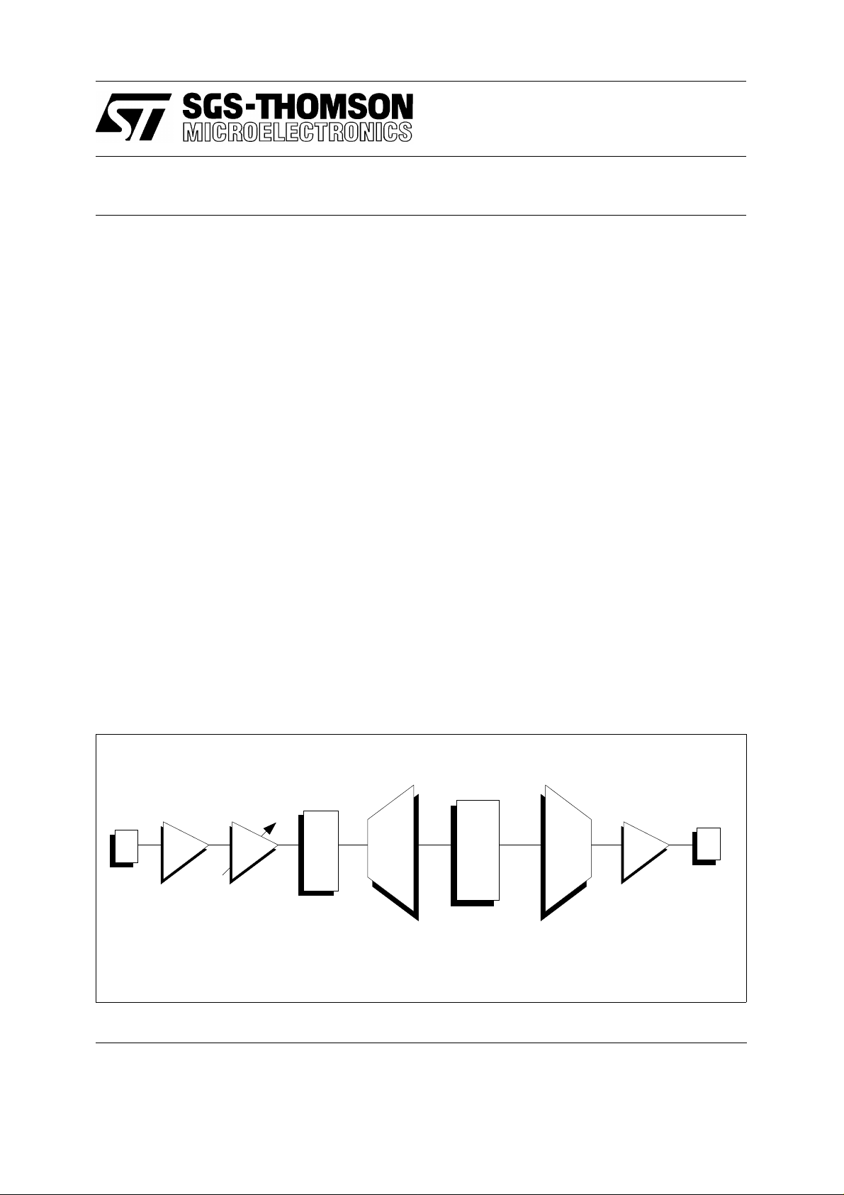
Figure 1 : The STKM2000 Series, a complete system solution
SENSOR
A
A
~
A / D
~
CONVERTER
D S P
~
BIP : GB = 100MHz
MOS : GB = 10MHz
November 1989
f = 150kHz
C(MAX)
12 Bits 1/2 Bit
+
-
µ
15 s
f
MAX
= 30MHz
D / A
CONVERTER
12 Bits 1/2 Bit
+
-
15 s
µ
ACTUATOR
A
500 mA max.
1/10

STKM2000 SERIES
STKM2000 ARCHIT ECTURE
Tech no logy
The STKM2000 Series developed by
SGS-THOMSON Microelectronics uses an
advanced BICMOS silicon gate process with dual
polysilicon layers and dual metal layers. This
process is optimized to achieve high performance
in digital CMOS applications. Depending on the
operating supply voltage (10V, or 5V), the CMOS
process behaves as an N-WELL technology
(respectively with 2 µ gate length or 1.8 µ gate
length) with operating speeds up to 30MHz.
Thanks to the two metal layers, the digital part of
the circuit can reach high gate density with low
parasitic capacitances .
For analog functions, the STKM2000 series takes
advantage of the bipolar structure:
Peripheral cells surround the internal active chip
area to interface with its external environment.
Despite the row based architecture, “hard blocks”
can be implemented with efficient floor planning
organization.
STKM2000 Cell lib rari es
SGS-THOMSON Microelectronics introduces the
“programmable” library; instead of working with a
finite number of cells of the library , the designer has
now access to an infinite number of functions.
Defining only some properties, the designer is able
to create himself the cells needed for his
application. For example, the following electrical
parameters are accessible and adjustable:
● very high speed NPN transistor : f
● very high speed vertical PNP : f
= 6 GHz
T
= 2.5 GHz
T
This allows high gain - bandwith operational
amplifier (50 MHz), low noise input amplif ier, short
propagation delay comparator, ...
With the same BICMOS process, the analog
CMOS performance come from the high density
CMOS structure with a double poly layer for
accurate capacitors, low consumption CMOS
amplifier (30 µA), CMOS switches, high accuracy
switched capacitor filter s (up t o 100 kH z f or cent er
frequency).
STKM2000 cell concepts
SGS-THOMSON Microelectronics has
predesigned and precharacterized c ells which are
selected, placed and interconnect ed on the chip to
implement digital and analog cells having different
height and supply voltages. In addition some
macrocells are designed as fixed bloc ks , s o called
“hard blocks” : filters, A/D and D/A conv erters; some
hard blocks are automatically generated and
parametrized from a compiler: S.C. filters, PLA,
RAM, ROM. ..
● gain-bandwith product
● phase margins, frequency compensation
● output buffer cur rent
● biasing currents
● resistor, capacitor fields
● current, source or sink
● adjustable Ron switch resistor
● supply voltage assignment
The analog library is operating in a large voltage
range: 3V to 10V.
The basic analog library contains:
● 60 analog CMOS functions
● 25 analog BIPOLAR functions
From single transitor to 12 bits A to D converter
(with autocalibration), each setup becomes
possible.
The digital CMOS library uses the same flexibility
with a complete set of basic digital functions
(NAND, NOR, Flip-Flop, ...) and some cell
generators:
STKM2000 chip topology
The chip is optimized versus the cell com plexity , in
a row based structure with different heights.
2/10
®
● register, counter, logic comparator, ...
More than 60 digital cells are available.
Figure 2: The STKM2000 Series, a complete system solution
ANALOG LI BRARY
NPN transistor P input CMOS Op-Amp
Lateral PNP Crystal oscillator
Substrate PNP RC oscillator
Isolated PNP Transconductance
NPN input comparator Power-on reset
PNP input comparator (with adjustable threshold and hysteresis)
N input comparator Analog multiplexer
P input comparator Voltage to current converter
N-MOS transistor Voltage reference
P-MOS tr ansis tor 8 bits, A/D and D/A converters
NPN high-speed amplifier 12 bits A/D and D/A converters
N input CMOS Op-Amp
STKM2000 SERIES
DIGITAL LIBRARY
AND, NAND, OR , NO R, invert er Shift register
Exclusive OR, NO R Binary counter
D latch Decimal counter
Input buffer (TTL/CMOS) Magnitude comparator
Output buffer (TTL/CMOS)
3/10
®

STKM2000 SERIES
CAD SUPPORT: A.D. S. (Analog Design Sys tem )
SGS-THOMSON Microelectronics has introduced
a sophisticated CAD approach to reduce the
development leadtime and to increase design
flexibility and safety.
Programm able cells in the library are defined as:
● alternative cell or,
● adjustable cell or ,
● telescopic cell or,
● parametrisable cell
Some specific parts of the des ign are automatic ally
handled by an analog design manager, in order to:
● reduce capture errors
● make unexperienced designer’s task easier
● improve schematics lisibility
● check electrical design rules (Analog or Digital)
The Analog Design manager takes into account :
● transconduct ance block generat ion
● automatic cell biasing
● unconnected pins and power down processing
● multipower supplies processing
A major step has been made with the introduction
of function generator and compiler approaches to
improve design automation and design efficiency.
Operation al amp li fier g enerat or
From a generic symbol and some properties,
several parameters of the amplifier will be adjusted:
● Biasing current which c ontrols major parameters
of amplifier (gain-bandwidth, slew rate, power
consumption).
● Frequency compensat ion which allows to adjust
and optimize the dynamic parameters vers us the
capacitive and resistive load.
● Power down capabilities.
● Supply voltage of the cell.
A specific software manages all these properties
and automatically updates all libraries included in
the design flow: macro models and transistor level
models, footprint, GDS2 layout , LVS netlist.
Figure 3: Analog Design System (A. D.S .) flow
DIGITAL
D
Generator
Top Level
Simulation
SABER
Digital
HILO 3
D
Analog
Simulation
ST SPICE
Digital
Models
Simulation
Schematic
Capture
Data Base
Netlist
Extractor
Behavioral
Models
Transistor
Models
Back Annotation
Digital Analog
Symbols
Filter Compiler
Analog Generator
Programmable Cells
G
Generation
G
Place & Route
GDSII File
DRC/LVS
G
G
Cells Boxes
Cells
Layout
G
G
4/10
PG Tape
®

STKM2000 SERIES
Filter compiler
From the template defined at the beginning up to
the complete layout, the software handles
automatically the filter synthesis and the layout
compilation:
● evaluation/mathematical analysis
● switched capacitor synthesis
● simulation
● Monte-Carlo analysis
● layout generation
Any kind of filters is available from 2nd up to 12th
order.
Digital cell gen erato r
For a set of basic digital cells , the us er has acces s
to generators which handle the netlists and
interface with the layout tools.
Schematic capture
(SILVAR LISCO
Logic simulation
(GENRAD
Analog simulation
Top level simulation
Layout
DRC - LVS
ST-SPICE ST-SPICE
(SGS-THOMSON) (SGS-THOMSON)
(ANALOGY
(SILVAR LISCOTM) EDGE (CADENCETM)
DRACULA EDGE
(CADENCE
The schematic capture uses a block which is
programmable according to the required
complexity.
The generator creates a “ so-called” sof t macr ocell
taking into account the complete netlist:
● counters
● shift registers
● magnitude comparators , .. .
A part from the software automation, the A.D.S.
CAD tool works around standard softwares .
The CAD approach is compatible with both
approaches:
● VA X
● SUN
VAX
TM
CASS EDGE
HILO 3 MOZART
TM
SABER SABER
TM
CALMP
TM
/VMS operating syst em
TM
/UNIX operating system
TM
SUN
TM
) (CADENCETM)
TM
) (SGS-THOMSON)
) (ANALOGYTM)
) (CADENCETM)
5/10
®

STKM2000 SERIES
Customer design interface
SGS-THOMSON Micorelectronics has developed
several interfaces for customers giving them easy
and flexible design approac hes f or STKM2000.
Users can access Analog Design Syst em (A.D.S .):
● via SGS-THOMSON design centers
● via SGS-THOMSON associated design centers
● via CAE workstations
CAE worstation capabilities are under
development on:
Figure 4: SGS-THOMSON - CUSTOMER interfaces
Interface 2 Interface 3 Interface 4
Responsibility level
Circuit definition
Schematics
Breadboard schematics Simulated schematics Layout tape
Ctm
● Dazix Syst em
● Mentor Graphics
● Sun
In that case,direct interfaces w ill be offer ed in order
to make design im plementation wit h A.D .S. (layout
and test generations).
According to these design possibilities,
SGS- THO M SO N defines 3 main interfaces .
Figure 4 outlines these interfaces. Each interface
details the responsibilities of custom er and
SGS-THOMSON during circuit development flow.
Ctm
Ctm
Simulations
Layout
Final control
Prototyping phase
ST
ST + Ctm
ST
ST
ST + Ctm
ST
ST + Ctm
ST
6/10
®

STKM2000 SERIES
MAXIMUM RATINGS
Symbol Parameter Min Max Unit
V
DD
V
, V
I
O
I
, I
I
O
T
stg
Supply voltage
I/O voltage
I/O current
storage temp. (ceramic)
storage temp. (plastic)
Note 1: Stresses above those under “maximum
ratings” may cause permanent damage to the
device. This is a stress rating only and functional
operation for the device at these or any other
- 0.5 12.0 V
- 0.5 V
+ 0.5 V
DD
- 40 + 40 nA
- 65 + 150
- 40 + 125
conditions above indicated in the operational
sections of this specification is not implied.
Exposure to absolute maximum rating conditions
for extended periods may affect device reliability.
RECOMMENDED DC OPERATING CONDITIONS
Voltage referred to V
Symbol Parameter Min Max Unit
V
DD
T
amb
SS
Operating supply voltage
Operating ambient temperature
Military
Industrial
Commercial
2.7 11 V
- 55 + 125
- 40 + 85
0 + 70
o
C
o
C
o
C
o
C
o
C
DIGITAL LIBRAR Y AC EL ECTRICAL CHARACTERI STICS ABSTRACT
Standard condition = 2 loads + 1 mm of metal interconnect
= 10V ± 10%, T = 25oC
V
Cell code Description
IV1
ND2
NR2
FD1
Standard inverter
2 - input NAND
2 - input NOR
D Flip - Flop
From C to QN
TSU
TH
TWH
TWL
OB11
CMOS inverting output buffer
capacitance load = 100 pF
DD
TPHL TPLH OTHER
2.26 2.01 ns
1.74 2.44 ns
2.55 2.02 ns
6.44 8.26
12.4 12.3 ns
Unit
5.00
1.75 ns
8.25
5.00
7/10
®

STKM2000 SERIES
DC GENERAL ELECTRICAL CHARACTERISTICS
= 5V ± 10% or VDD = 10V ± 10% (unless otherwise specified)
V
DD
Symbol Parameter Condition Min Typ Max Unit
V
V
V
V
I
OZH
I
OZL
I
I
I
IH
IL
IH
IL
IH
IL
CC
High level TTL input voltage VDD = 5V ± 10%
o
= 0oC / + 70oC
T
o
T
= - 40oC / + 85oC
o
T
= - 55oC / + 125oC
Low level TTL input voltage VDD = 5V ± 10%
all temp. ranges
High level CMOS input voltage
Low level CMOS input voltage
Tristate output leakage current VO = V
DD
To = 0oC / + 70oC
o
T
= - 40oC / + 85oC
o
T
= - 55oC / + 125oC
VO = V
SS µA
o
T
= 0oC / + 70oC
o
T
= - 40oC / + 85oC
o
T
= - 55oC / + 125oC
High level input leakage current VO = V
DD
To = 0oC / + 70oC
o
T
= - 40oC / + 85oC
o
T
= - 55oC / + 125oC
Low level input leakage current VI = V
SS
To = 0oC / + 70oC
o
T
= - 40oC / + 85oC
o
T
= - 55oC / + 125oC
Max admissible current per pin:
- analog
- digital
2.0 V
2.25 V
2.25 V
0.8 V
70%VDD V
30%VDD V
2.5 µA
5 µA
10 µA
- 2.5 µA
- 5.0 µA
- 10.0 µA
1.0 µA
3.0 µA
5.0 µA
- 1.0 µA
- 3.0 µA
- 5.0 µA
± 20 mA
± 40 mA
V
8/10
®

STKM2000 SERIES
ANALOG LI BRARY AC ELECTRICAL CHARACTERISTICS ABSTRACT
Cell code Description Parameters Min Typ Max Unit
Test conditions
CMP11
CMP31
CPX11
CPP11
RPM/PPM
SWI1
MN11
OPA31
OPA41
OPA71
OTA11
POR11
VRF11
Static CMOS Propagation delay
comparator (overdrive = 5 mV)
Offset
Static BICMOS Propagation delay
comparator (overdrive = 5 mV)
Offset
Capacitor fields Unit capacitance
Capacitor value range
Absolute accuracy
Matching (capacitor ratio)
Monolithic Capacitor Capacitor range
Absolute accuracy
Resistor/Potentiometer Resistor value range
P-Base Absolute accuracy
Matching
Temperature coefficient
Voltage coefficient
Analog switch Elementary switch RON value
Number of switches in parallel
Telescopic NMOS RON value
transistor
General purpose Unity gain bandwidth
MOS Operational Current consumption
amplifier Phase margin
(C1 = 100 pF, R2 = 10 kΩ)
Offset
Internal bipolar Unity gain-bandwidth
Operational Amplifier current consumption
Phase margin
(CL = 15 pF, RL = 100kΩ)
Offset
Rail to rail external Unity gain bandwidth
MOS operational current consumption
Amplifier Phase margin
(CL = 100 pF, RL = 100KΩ)
Offset
MOS Unity gain - bandwidth
transconductance (CL = 2 pF)
amplifier
Programmable Power
on Reset
Active Level Accuracy
Hysteresis Accuracy
Voltage bandgap Output voltage accuracy
reference Temperature coefficient
Current consumption
1 1.4 ms
± 3 ± 10 mV
90 110 ns
± 2 ± 7mV
0.1 pF
0.1 50 pF
± 15 %
0.5 1.0 %
1 100 pF
± 15 %
6.5 3000 KΩ
± 20 %
± 1%
0.2 %
0.05 %
525KΩ
13
100 Ω
3.3 4.6 MHz
700 µA
60
± 3 ± 10 mV
9 30 MHz
240 µA
62
± 1 ± 5mV
2.3 MHz
360 uA
80
± 3 ± 10 mV
24 MHz
± 5
± 5
± 2%
100 ppm
15 µA
o
o
o
%
%
9/10
®

STKM2000 SERIES
ANALOG LI BRARY AC ELECTRICAL CHARACTERISTICS ABSTRACT
Cell code Description Parameters Min Typ Max Unit
Test conditions
OSC11
OSC41P
OSC31P
ADC81
DAC81
Programmable crystal Frequency
oscillator
RC oscillator Frequency
Stability versus temperature
Stability versus voltage
One pad I.C oscillator Frequency
Stability versus temperature
Stability versus voltage
Filters Order
Center frequency
8 bit analog to Conversion time
digital converter Integral non linearity
Differential non linearity
8 bit analog to Conversion time
digital converter (CL = 2 pF)
Integral non linearity
0.1 20 MHz
1 100 800 KHz
0.01 % /
0.5 % / V
2 200 KHz
0.01 % /
0.5 % / V
212
100 KHz
5 µs
± 0.5 LSB
± 0.5 LSB
1 µs
± 0.5 LSB
o
C
o
C
Information furnished is believed to be accurate and reliable. However, SGS-THOMSON Microelectronics assumes no
responsability for the consequences of use of such information nor for any infringement of patents or other rights of third
parties which may result from its use. No license is granted by implication or otherwise under any patent or patent rights
of SGS-THOMSON Microelectronics. Specifications mentioned in this publication are subject to change without notice.
This publication supersedes and replaces all information previously supplied.
SGS-THOMSON Microelectronics products are not authorized for use as critical components in life support devices or
systems without the express written approval of SGS-THOMSON Microelectronics.
Purchase of I
ponents in an I
Australia - Brazil - France - Germany - Hong Kong - Italy - Japan - Korea - Malaysia - Malta - Morocco - The Netherlands
2
C Components by SGS-THOMSON Microelectronics conveys a license under the Philips I2C Patent. Rights to use these com-
2
C system is granted provided that the system conforms to the I2C Standard Specification as defined by Philips.
Singapore - Spain - Sweden - Switzerland - Taiwan - Thailand - United Kingdom - U.S.A.
© 1994 SGS-THOMSON Microelectronics - All rights reserved.
SGS-THOMSON Microelectronics Group of Companies
10/10
®
 Loading...