

SGS Thomson Microelectronics ST92T163R4T1V, ST92T163R4T1L, ST92T163R4T1E, ST92T163R4T1, ST92T163N4B1E Datasheet
...
January 2000 1/224
This ispreliminary information on a newproductin developmentorundergoing evaluation. Details are subject tochangewithout notice.
ST92163
8/16-BIT FULL SPEED USB MCU FOR COMPOSITE DEVICES
WITH 16 ENDPOINTS, 20K ROM, 2K RAM, I2C, SCI, & MFT
PRELIMINARY DATA
■ Internal Memories: 20 Kbytes ROM/EPROM/
OTP, 2 Kbytes RAM
■ Register oriented 8/16 bit core
■ 224 general purpose registers available as
RAM, accumulators or index pointers
■ Minimum instruction cycle time: 167 ns (@24
MHz CPU frequency)
■ Low power modes: WFI, SLOW, HALT and
STOP
■ DMA controller for reduced processor overhead
■ Full speed USB interface with DMA, compliant
with USB specifications version 1.1 (in normal
voltage mode)
■ USB Embedded Functions with 16 fully
configurable endpoints (buffer size
programmable), supporting all USB data
transfer types (Isochronous included)
■ On-chip USB transceiver and 3.3 voltage
regulator
■ Multimaster I
2
C-bus serial interface up to
400KHz. with DMA capability
■ Serial Communications Interface (SCI) with
DMA capability:
– Asynchronous mode up to 315 Kb/s
– Synchronous mode up to 3 MHz
■ External memory interface (8-bit data/16-bit
address) with DMA capability from the USB
■ 16-bit Multi-Function Timer (12 operating
modes) with DMA capability
■ 16-bit Timer with 8-bit prescaler and Watchdog
■ 6-channel, 8-bit A/D Converter (ADC)
■ 15 interrupt pins on 8 interrupt channels
■ 14 pins programmable as wake-up oradditional
external interrupts
■ 42 (DIP56) or 44 (QFP64) fully programmable
I/Os with 6 or 8 high sink pads (10 mA @ 1 V)
■ Programmable PLL clock generator (RCCU)
using a low frequency external quartz (8 MHz)
■ On-chip RC oscillator for low power operation
■ Low Voltage Detector Reset on some devices
1
■ Rich instructionset with 14 addressing modes
■ Several operating voltage modes available on
some devices1:
– Normal Voltage Mode
– 8-MHz Low Voltage Mode
– 16-MHz Low Voltage Mode
■ 0 -24 MHzCPU clockoperation @4.0-5.5 V(all
devices)
■ 0 - 8 MHz CPU clock operation @ 3.0-4.0 V (8-
MHz and 16-MHz Low Voltage devices)
■ 0 - 16 MHz CPU clock operation @ 3.0-4.0 V
(16-MHz Low Voltage devices only)
■ Division-by-zero trap generation
■ 0
o
Cto70oC temperature range
■ Low EMI design supporting single sided PCB
■ Complete development tools, including
assembler, linker, C-compiler, archiver, source
level debugger and hardware emulators, and
Real Time Operating System
Note 1: Refer to “DeviceSummary” onpage 6
1
TQFP64
PSDIP56
Rev. 1.9

2/224
Table of Contents
ST92163 ............................................1
1 GENERAL DESCRIPTION . . . . . . ................................................ 6
1.1 INTRODUCTION . . . . . . . . . . . . ............................................. 6
1.1.1 Core Architecture . . . . . . . . . . . . . . . . . .................................. 9
1.1.2 Instruction Set . . . . . . . . . .. . . . . . . . . . .................................. 9
1.1.3 External MEMORY INTERFACE . . . . . . . . . . . . . . . . . . . . . . . . . . ............. 9
1.1.4 OPERATING MODES . . . . . . . . . . . . . . . . . . . . . . . . . . . . . . . . . . . . . . . . . . . . . . . 9
1.1.5 On-chip Peripherals . . . . . . . . . . . . . . . . . . . . . . . . . . . . .................... 10
1.2 PIN DESCRIPTION . . .................................................... 11
1.3 I/O PORT PINS . . . . . . . . . . . . . . . . . ........................................13
1.4 MEMORY MAP . . . . . . . . . . ...............................................19
1.5 ST92163 REGISTER MAP ................................................ 20
2 DEVICE ARCHITECTURE . . . . . . . . . . ........................................... 27
2.1 CORE ARCHITECTURE . . . . . . . . . . . . . . . . . . ................................27
2.2 MEMORY SPACES . . . . . . . . . . . . . . ........................................ 27
2.2.1 Register File . . . . . . . . . . . . . . . . .. . . . . . . .............................. 27
2.2.2 Register Addressing . . . . . ...........................................29
2.3 SYSTEM REGISTERS . . . . . . . .. . . . . . . . . . . . . . .............................. 30
2.3.1 Central Interrupt Control Register . . . . . . . . . . . ........................... 30
2.3.2 Flag Register . . . . . . ............................................... 31
2.3.3 Register Pointing Techniques . ........................................ 32
2.3.4 Paged Registers . . . . . . . . . . . . . . . . . . . . . . . . . . . . . . . .. . . . . . . . . . . . . . . . . . . 35
2.3.5 Mode Register . . . . . ............................................... 35
2.3.6 Stack Pointers . . . . . . . . . . . . . . . . . . . . . ................................36
2.4 MEMORY ORGANIZATION . . . . . . . . . . . . . . . ................................. 38
2.5 MEMORY MANAGEMENT UNIT . . . . . . . . . . .................................. 39
2.6 ADDRESS SPACE EXTENSION . . . . . . . . . . . . . . . . . . . . . . . . .. . . . . . . . . . . . . . . . . . . 40
2.6.1 Addressing 16-Kbyte Pages . . . . . . . . . .................................40
2.6.2 Addressing 64-Kbyte Segments . . . . . .................................. 41
2.7 MMU REGISTERS . ...................................................... 41
2.7.1 DPR[3:0]: Data Page Registers . . . . . . .. . . . . . . . . . . . . . . . . . . . . ...........41
2.7.2 CSR: Code Segment Register ........................................ 43
2.7.3 ISR: Interrupt Segment Register . . . . . . . . . .............................. 43
2.7.4 DMASR: DMA Segment Register . . . . . . . . .............................. 43
2.8 MMU USAGE . . . . . . . . . . . . . . . . . . . . . . . . . . ................................. 45
2.8.1 Normal Program Execution . . . . . . . . . . . . . . . . . . . . . . . . . . . . ............... 45
2.8.2 Interrupts . . . . . . . . . . . . . . . . . . . .. . . . . . . .............................. 45
2.8.3 DMA . . . . . . . . . . . . . . . . . . . . . . . . . . . . . . . . . ........................... 45
3 INTERRUPTS . . ............................................................. 46
3.1 INTRODUCTION . . . . . . . . . . . . ............................................46
3.2 INTERRUPT VECTORING ................................................ 47
3.2.1 Divide by Zero trap . . . . . . . . . . . . . . . . ................................. 47
3.2.2 Segment Paging During Interrupt Routines . ............................. 48
3.3 INTERRUPT PRIORITY LEVELS . . . . . . .. . . . . . . . . . . . . . . . . . . . . . . . . . . . . . . . . . . . 48

3/224
Table of Contents
224
3.4 PRIORITY LEVEL ARBITRATION . . . ........................................48
3.4.1 Priority level 7 (Lowest) . . . . . . . . . . . . . . . . . . . . . . . . . . . . . . . . . . . . . . . . . . . . . 48
3.4.2 Maximum depth of nesting . . . ........................................48
3.4.3 Simultaneous Interrupts . . . . . . . . . . . . ................................. 48
3.4.4 Dynamic Priority Level Modification . . . . . . . . . . . . . . . . . . . . . . . . . . . . . . . . . . . . 49
3.5 ARBITRATION MODES . . . . . . . . . . . . . . . . . .................................. 49
3.5.1 Concurrent Mode . . . . . . . . . . . . . . . . . . . . . . . . . . . . . . . . . . . . . . . . . . .. . . . . . . 49
3.5.2 Nested Mode . . . . . . ............................................... 52
3.6 EXTERNAL INTERRUPTS . . . . . . . . . . .. . . . . . . .............................. 54
3.7 MANAGEMENT OF WAKE-UP LINES AND EXTERNAL INTERRUPT LINES . ........ 56
3.8 TOP LEVEL INTERRUPT . . . . . . . . . . . . . . . . . ................................57
3.9 ON-CHIP PERIPHERAL INTERRUPTS . . . . . . . . . . . . . . . . . . . .. . . . . . . ...........57
3.10INTERRUPT RESPONSE TIME . ...........................................58
3.11INTERRUPT REGISTERS . . ...............................................59
3.12WAKE-UP / INTERRUPT LINES MANAGEMENT UNIT (WUIMU) . . . . . . . . . . . . . . . . . . 63
3.12.1 Introduction . . . . . . . . . . . . . . . ........................................ 63
3.12.2 Main Features . . . . . . . . . . . . . . . . . . . . . . . . . . . . . . . . . . . . . . . . . . . . . ........ 63
3.12.3 FunctionalDescription . . . . . . . . . . . . . . . . . . . . . . . . . . . . . . . . . . . . . . . . . . . . . . 64
3.12.4 ProgrammingConsiderations . . . . . . . . . . . . . . . . . . . . . . . . . . ............... 66
3.12.5 Register Description . ............................................... 67
4 ON-CHIP DIRECT MEMORY ACCESS (DMA) . . . . .................................. 70
4.1 INTRODUCTION . . . . . . . . . . . . . ...........................................70
4.2 DMA PRIORITY LEVELS . . . ...............................................70
4.3 DMA TRANSACTIONS . . . . . . . . . . . ........................................71
4.4 DMA CYCLE TIME . . . . . . . . . . . . . . . ........................................ 73
4.5 SWAP MODE . . . . . . . . . . . . ...............................................73
4.6 DMA REGISTERS . . . . . . . . . . . . ........................................... 74
5 RESET AND CLOCK CONTROL UNIT (RCCU) . . . .................................75
5.1 INTRODUCTION . . . . . . . . . . . . . ...........................................75
5.2 CLOCK CONTROL UNIT . . . . . . ............................................75
5.2.1 Clock Control Unit Overview . . ........................................75
5.3 CLOCK MANAGEMENT . . . . . . . . . . ........................................77
5.3.1 PLL Clock Multiplier Programming . . . . .................................78
5.3.2 CPU Clock Prescaling . . . . . . . . . . . . . . . . . . . . . . . . . . . . . . . . . . . . . . . . . . . . . . 78
5.3.3 Peripheral Clock . . . . . . . . . . . . . . . . . . . . . . . . . . . . . . . . . . . . . . . . . . . . . .. . . . . 78
5.3.4 Low Power Modes . . . . . . . . . . . . . . . . . . . . . . . . . . . . . . . . . . . . . . . . . ........ 79
5.3.5 Interrupt Generation . . . . . . . . . . . . . . . . . . . . . . . . . . . . .................... 79
5.4 CLOCK CONTROL REGISTERS . . . . . . . . . . . . . . .............................. 81
5.5 OSCILLATOR CHARACTERISTICS . . . . . . . . . . . .............................. 85
5.6 RESET/STOP MANAGER . . . . . . ...........................................86
5.6.1 Reset Pin Timing . . . ............................................... 87
5.7 STOP MODE . . . . . . . . .. . . . . . . . . . ........................................ 87
5.8 LOW VOLTAGE DETECTOR (LVD) RESET . . ................................. 88

4/224
Table of Contents
6 EXTERNAL MEMORY INTERFACE (EXTMI) . . . . . . . . . . . . . . . . . . . . . . . . . . . . . . . . . . . . . . 89
6.1 INTRODUCTION . . . . . . . . . . . . . ...........................................89
6.2 EXTERNAL MEMORY SIGNALS .. . . . . . . . . . . . . . . . ........................... 90
6.2.1 AS: Address Strobe . . . . . . . . . . . . . . . . . . . . . ........................... 90
6.2.2 DS: Data Strobe . . . . ...............................................90
6.2.3 DS2: Data Strobe 2 . . . . . . . . . . . . . . . . . . . . . . . . . . . . . . . . . . . . . . . . . . . . . . . . . 90
6.2.4 RW: Read/Write . . . . ............................................... 93
6.2.5 BREQ, BACK: Bus Request, Bus Acknowledge . . . . . . . . . . . . . . . . . . . ........ 93
6.2.6 PORT 0 . . . . . . .................................................... 94
6.2.7 PORT 1 . . . . . . .................................................... 94
6.2.8 WAIT: External Memory Wait . . . . .. . . . . . . . . . . . . . . . . . . . . ............... 94
6.3 REGISTER DESCRIPTION . ............................................... 95
7 I/O PORTS . . . . . . . . .. . . . . . . . . . . . . . . . . ........................................ 98
7.1 INTRODUCTION . . . . . . . . . . . . . ...........................................98
7.2 SPECIFIC PORT CONFIGURATIONS . . . . . . . . . . . . . . . . . . . . .. . . . . . . . . . ........ 98
7.3 PORT CONTROL REGISTERS . . . . . . . . . . . . . . . . . . ........................... 98
7.4 INPUT/OUTPUT BIT CONFIGURATION . . . . . . . . . . . . . . . . . . . . . . . . . .. . . . . . . . . . . . 99
7.5 ALTERNATE FUNCTION ARCHITECTURE . . . . . . . . . . . . . . . . . . . . . . . . ..........103
7.5.1 Pin Declared as I/O . . .............................................. 103
7.5.2 Pin Declared as an Alternate Input . . . . . . . . . . . . . . . . . . . . . . . . . . . . . . . . . . . . 103
7.5.3 Pin Declared as an Alternate Function Output . . . . . . . . . . . . . . . . . . . . . . . . . . . 103
7.6 I/O STATUS AFTER WFI, HALT AND RESET . . . . . . . . . . . . . . .. . . . . . . ..........103
8 ON-CHIP PERIPHERALS . . . . . . . . . . . ..........................................104
8.1 TIMER/WATCHDOG (WDT) . . . . . . . . . . . . . ................................. 104
8.1.1 Introduction . . . . . . . . . . . . .......................................... 104
8.1.2 Functional Description . . . . . . ....................................... 105
8.1.3 Watchdog Timer Operation . . . . . . . ................................... 106
8.1.4 WDT Interrupts ................................................... 108
8.1.5 Register Description . . . . . ..........................................109
8.2 MULTIFUNCTION TIMER (MFT) . . . . . . . . . . . . . . . . . . . . . . . . ................... 111
8.2.1 Introduction . . . . . . . . . . . . .......................................... 111
8.2.2 Functional Description . . . . . . ....................................... 113
8.2.3 Input Pin Assignment . . . . . . . . . . . . . ................................. 116
8.2.4 Output Pin Assignment . . . . . .. . . . . . . . . . . . . . . . . . . . . . . . . . . . . . . . . . . . . . . 120
8.2.5 Interrupt and DMA . . . . . . . . . . . . . . . . ................................ 122
8.2.6 Register Description . . . . . ..........................................124
8.3 USB PERIPHERAL (USB) . . ..............................................135
8.3.1 Introduction . . . . . . . . . . . . .......................................... 135
8.3.2 Main Features . . . . . . . . . ...........................................135
8.3.3 Functional Description . . . . . . ....................................... 135
8.3.4 Register Description . . . . . ..........................................138
8.3.5 Register pages summary . . . . . . . . . . . ................................ 148
8.4 SERIAL COMMUNICATIONS INTERFACE (SCI) . . . . . . . . . . . . . . . . . . . . . . . . . . . . . . 150
8.4.1 Introduction . . . . . . . . . . . . .......................................... 150
8.4.2 Functional Description . . . . . . ....................................... 151
8.4.3 SCI Operating Modes . . . . . . . . . . . . . . . . . . . . . . . . . . . . . . . . . . . . . . . . . . . . . . 152

5/224
Table of Contents
224
8.4.4 Serial Frame Format . . . . . . . . . . . . . . . . . . . . . . . . . . . . . . . . . . . . . . . . . . . . . . . 155
8.4.5 Clocks And Serial Transmission Rates . ................................ 158
8.4.6 SCI Initialization Procedure . . . . . . . . . . . . ............................. 158
8.4.7 Input Signals . . . . . . . . . . . . . . ....................................... 160
8.4.8 Output Signals . . . . . . . . . . . . . . . . . . . . . . . . . . . . . . . . . . . . . . . . . . . . ....... 160
8.4.9 Interrupts and DMA . . . . . . . . . .......................................161
8.4.10 Register Description . ..............................................164
8.5 I2C BUS INTERFACE . . . . . . . . . . . . . . .. . . . . . . ............................. 175
8.5.1 Introduction . . . . . . . . . . . . .......................................... 175
8.5.2 Main Features . . . . . . . . . ...........................................175
8.5.3 Functional Description . . . . . . ....................................... 176
8.5.4 I2C State Machine . . .............................................. 178
8.5.5 Interrupt Features . . . . . . . . . . .......................................183
8.5.6 DMA Features . . . . . . .............................................. 184
8.5.7 Register Description . . . . . ..........................................186
8.6 A/D CONVERTER (A/D) . . . . . . . . . . . . . . . . . ................................ 197
8.6.1 Introduction . . . . . . . . . . . . .......................................... 197
8.6.2 Main Features . . . . . . . . . ...........................................197
8.6.3 General Description . . . . . . . . . . . . . . . . . . ............................. 197
8.6.4 Register Description . . . . . ..........................................199
9 ELECTRICAL CHARACTERISTICS . . . . . . . . . . . . . . . . .............................201
10 GENERAL INFORMATION ................................................... 218
10.1EPROM/OTP PROGRAMMING . . . . . . . . . . . . . . . . . . . . . . . . . ................... 218
10.2PACKAGE DESCRIPTION . . . . . . . . . . . . . . . . . . . . . . . . . . . . . . . . . . . . . . . . . . .. . . . 219
10.3ORDERING INFORMATION . . . . . . . . . . . . . ................................. 221
10.4TRANSFER OF CUSTOMER CODE . .......................................221
6/224
ST92163 - GENERAL DESCRIPTION
1 GENERAL DESCRIPTION
1.1 INTRODUCTION
The ST9216x family brings the enhanced ST9 register-based architecture to a new range of highperformance microcontrollers specifically designed for USB (Universal Serial Bus) applications. Their performance derives from the use of a
flexible 256-register programming model for ultrafast context switching and real-time event response. The intelligent on-chip peripherals offload
the ST9 core from I/O and data management
processing tasks allowing critical application tasks
to get the maximum use of core resources. The
ST9 MCUdevices support low powerconsumption
and low voltage operation for power-efficient and
low-cost embeddedsystems. In the ST92163family, four different types of device are available:
Normal Voltage Devices with LVD function
They operate in Normal Voltage Mode only (4.0-
5.5V @ 24MHz) and include the Low Voltage Detector (LVD) function.
Normal Voltage Devices without LVD function
They operate in Normal Voltage Mode only (4.0-
5.5V @ 24MHz) and do not include the Low Voltage Detector (LVD) function.
8-MHz Low Voltage Devices
They do not include the Low Voltage Detector
(LVD) function and they support two operating
voltage modes:
– Normal Voltagemode (4.0-5.5V @ 24MHz) with
full functionality including USB.
– 8-MHz Low Voltage mode (3.0-4.0V @ 8MHz)
without the USB interface.
16-MHz Low Voltage Devices
They do not include the Low Voltage Detector
(LVD) function and they support three operating
voltage modes:
– Normal Voltagemode (4.0-5.5V @ 24MHz) with
full functionality including USB.
– 8-MHz Low Voltage mode (3.0-4.0V @ 8MHz)
without the USB interface.
– 16-MHzLow Voltagemode (3.0-4.0V @ 16MHz)
without the USB interface.
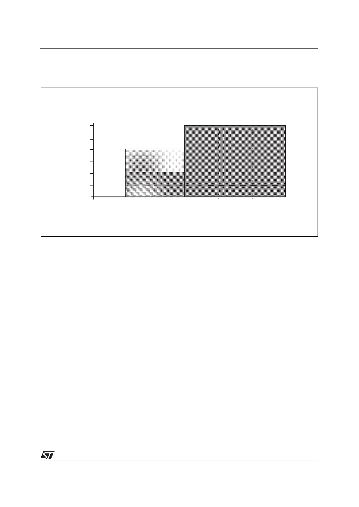
Figure 1, on page 7 shows the operating range of
the ST92163 devices.
Device Summary
1
Contact sales office for availability
Device Package Program Memory RAM
16-MHz
Low Voltage
Mode
8-MHz
Low Voltage
Mode
LVD USB
ST92163
1
PSDIP56/
TQFP64
20K ROM
2K
No
No
Yes
Yes
ST92T163 20K OTP
ST92E163
CSDIP56/
CQFP64
20K EPROM
ST92163E
1
PSDIP56/
TQFP64
20K ROM
No
ST92T163E 20K OTP
ST92E163E
CSDIP56/
CQFP64
20K EPROM
ST92163L
1
TQFP64
20K ROM
Yes
In Normal
Mode only
ST92T163L 20K OTP
ST92E163L CQFP64 20K EPROM
ST92163V
1
TQFP64
20K ROM
YesST92T163V
1
20K OTP
ST92E163V
1
CQFP64 20K EPROM
7/224
ST92163 - GENERAL DESCRIPTION
INTRODUCTION (Cont’d)
Figure 1. Maximum Operating Frequency (f
MAX
) versus Supply Voltage (VDD)
Notes:
1) This mode is supported by 16-MHz Low Voltage devices only
2) This mode is supported by 8-MHz Low Voltage devices and 16-MHz Low Voltage devices
3) This mode is supported by all devices
0
2.5
4 4.5 5 5.5
24
20
16
12
8
4
MAX FREQUENCY (MHz)
SUPPLY VOLTAGE (V)
3.0
16-MHz LOW VOLTAGE
MODE
1)
FUNCTIONALITY IS NOT
GUARANTEED
IN THIS AREA
NORMAL VOLTAGE MODE
3)
8-MHz LOW VOLTAGE
MODE
2)
8/224
ST92163 - GENERAL DESCRIPTION
INTRODUCTION (Cont’d)
Figure 2. ST92163 Architectural Block Diagram
*64-pin devices only
**on some devices only (refer to “Device Summary” on page 6)
WATCHDOG
TIMER
256 bytes
Register File
2K RAM
ST9+ CORE
8/16-bit
CPU
Interrupt
Management
MEMORY BUS
RCCU
External
Memory
Interface
REGISTER BUS
A/D Converter
AS
BACK
BREQ
DS
WAIT
RW
P0[7:0]
SCI
20K ROM/
EPROM/OTP
AIN[5:0]
EXTRG
TXCLK
RXCLK
SIN
DCD
SOUT
CLKOUT
RTS
SDS
WDIN
WDOUT
All alternate functions (
Italic characters
) are mapped on Ports 0,1, 3, 4, 5 and 6
P3[7:0]
P1[7:0]
SDA
SCL
MF TIMER
USBGND
USBVCC
USBDM0
USBDP0
OSCIN
OSCOUT
RESET
INTCLK
I2C BUS
P5[7:0]
Fully Prog.
I/Os
TINA
TINB
TOUTA
TOUTB
INT[7:0]
NMI
P4[3:0]
P6[5:0]
USB
with 16 end-
points
Wakeup
and Interrupt
Management
WKUP[14:0]
P6[7:6]*
A[15:0]
D[7:0]
USBOE
DMA
DMA
9V/3.3V
Voltage
Regulator
Low Voltage
Detector
LVD**
USBSOF
MIRROR
REGISTER

9/224
ST92163 - GENERAL DESCRIPTION
INTRODUCTION (Cont’d)
1.1.1 Core Architecture
The nucleus of the ST92163 is the enhanced ST9
Core that includes the Central Processing Unit
(CPU), theregister file, theinterrupt and DMA controller, and the Memory Management Unit (MMU).
Three independent buses are controlled by the
Core: a 22-bit memory bus, an 8-bit register addressing bus and a 6-bit interrupt/DMA bus which
connects the interrupt and DMA controllers in the
on-chip peripherals with the core.
This multiple bus architecture makes the ST9 family devices highly efficient foraccessing on and
off-chip memory and fast exchange of data with
the on-chip peripherals.
The general-purpose registers can be used as accumulators, index registers, or address pointers.
Adjacent registerpairs make up 16-bit registersfor
addressing or 16-bit processing. Although the ST9
has an 8-bit ALU, the chip handles 16-bit operations, including arithmetic, loads/stores, and memory/register and memory/memory exchanges.
Many opcodes specify byte or word operations,
the hardware automatically handles 16-bit operations and accesses.
For interrupts or subroutine calls, the CPU uses a
system stack in conjunction with the stack pointer
(SP). A separate user stack has its own SP. The
separate stacks, without size limitations, can be in
on-chip RAM (or in Register File) or off-chip memory.
1.1.2 Instruction Set
The ST9 instruction set consists of 94 instruction
types, including instructions for bit handling, byte
(8-bit) and word (16-bit) data, as well as BCD and
Boolean formats. Instructions have been added to
facilitate large program and data handling through
the MMU, as well as to improve the performance
and code density of C Function calls. 14 addressing modes are available, including powerful indirect addressing capabilities.
The bit-manipulation instructions of the ST9 are
set, clear,complement, testand set, load,and various logic instructions (AND, OR, and XOR). Math
functions include add, subtract, increment, decrement, decimal adjust, multiply and divide.
1.1.3 External MEMORY INTERFACE
The ST92163device has a16-bit external address
bus allowingit toaddress up to 64K bytes of external memory.
1.1.4 OPERATING MODES
To optimize performance versus the power consumption of the device, ST9 devices now support
a range of operating modes that can be dynamically selected depending on the performance and
functionality requirements of the application at a
given moment.
Run Mode. This is the full speed execution mode
with CPUand peripherals running at the maximum
clock speed delivered by the Phase Locked Loop
(PLL) of the Clock Control Unit (CCU).
Slow Mode. Power consumption can be significantly reduced byrunning theCPU and theperipherals at reduced clock speed using the CPU Prescaler and CCU Clock Divider.
Wait For Interrupt Mode. The Wait For Interrupt
(WFI) instruction suspends program executionuntil an interrupt request is acknowledged. During
WFI, the CPU clock is halted while the peripheral
and interrupt controller keep running at a frequency programmable via the CCU. In this mode, the
power consumption of the device can be reduced
by more than 95% (LP WFI).
Halt Mode. When executing the HALT instruction,
and if the Watchdog is not enabled, the CPU and
its peripherals stop operating and the status of the
machine remains frozen (the clock is also
stopped). A reset is necessary to exit from Halt
mode.
Stop Mode. Under user program control, (see
Wake-up and Interrupt Management Unit), the
CPU and its peripherals stop operating and the
status of the machine remains frozen (the clock is
also stopped) until program execution is woken up
by an event on an external Wake-up pin.

10/224
ST92163 - GENERAL DESCRIPTION
INTRODUCTION (Cont’d)
1.1.5 On-chip Peripherals
USB Interface
The USB interface provides a full speed USB 1.1
compliant port with embedded transceiver and
voltage regulator. Upto 16 endpoints are available
supporting upto 8 USB devices.Separate transmit
and receive DMA channels are available for each
device for fast data transfers with internal RAM.
Parallel I/O Ports
The ST9 is providedwith dedicated lines for input/
output. These lines, grouped into 8-bit ports, can
be independently programmed to provide parallel
input/output or to carry input/output signals to or
from the on-chip peripherals and core. All ports
have active pull-ups and pull-down resistors compatible with TTL loads. In addition pull-ups can be
turned off for open drain operation and weak pullups can be turned on to save chip resistive pullups. Input buffers can be either TTL or CMOS
compatible.
High Current (10 mA) outputs are available for
driving external devices such as LEDs.
Multifunction Timer
The Multifunction Timer has a 16-bit Up/Down
counter supported by two 16-bit compare registers, two 16-bit input capture registers and two
DMA channels. Timing resolution can be programmed using an 8-bit prescaler. 12 operating
modes allow a range of different timing functions
to be easily performed suchas complex waveform
generatation, measurement or PWM output.
16-bit Timer/Watchdog
The Timer/Watchdog peripheral can be used as a
watchdog or for a wide range of other timing functions such asgenerating periodic interrupts,measuring input signal pulse widths, requesting an interrupt after a set number of events. It can also
generate a square wave or PWM output signal.
Serial Communications Controller
The SCIprovides a synchronous or asynchronous
serial I/O port using two DMA channels. Baud
rates and data formats are programmable. Controller applications can further benefit from the self
test and address wake-up facility offered by the
character search mode.
I2C Bus Interface
The I2C bus is a synchronous serial bus for connecting multiple devices using a data line and a
clock line. Multimaster and slave modes are supported. Data transfer between the bus and memory is performed by DMA. The I2C interface supports 7 and 10-bit addressing. It operates in multimaster or slave mode and supports speeds of up
to 400 KHz. Bus events (Bus busy, slave address
recognized) and error conditions are automatically
flagged in peripheral registers and interrupts are
optionally generated.
Analog/Digital Converter
The ADC provides up to 6 analog inputs with onchip sample and hold, fast conversion time and 8bit resolution. Conversion can be triggered by a
signal from the Multifunction Timer (MFT).
11/224
ST92163 - GENERAL DESCRIPTION
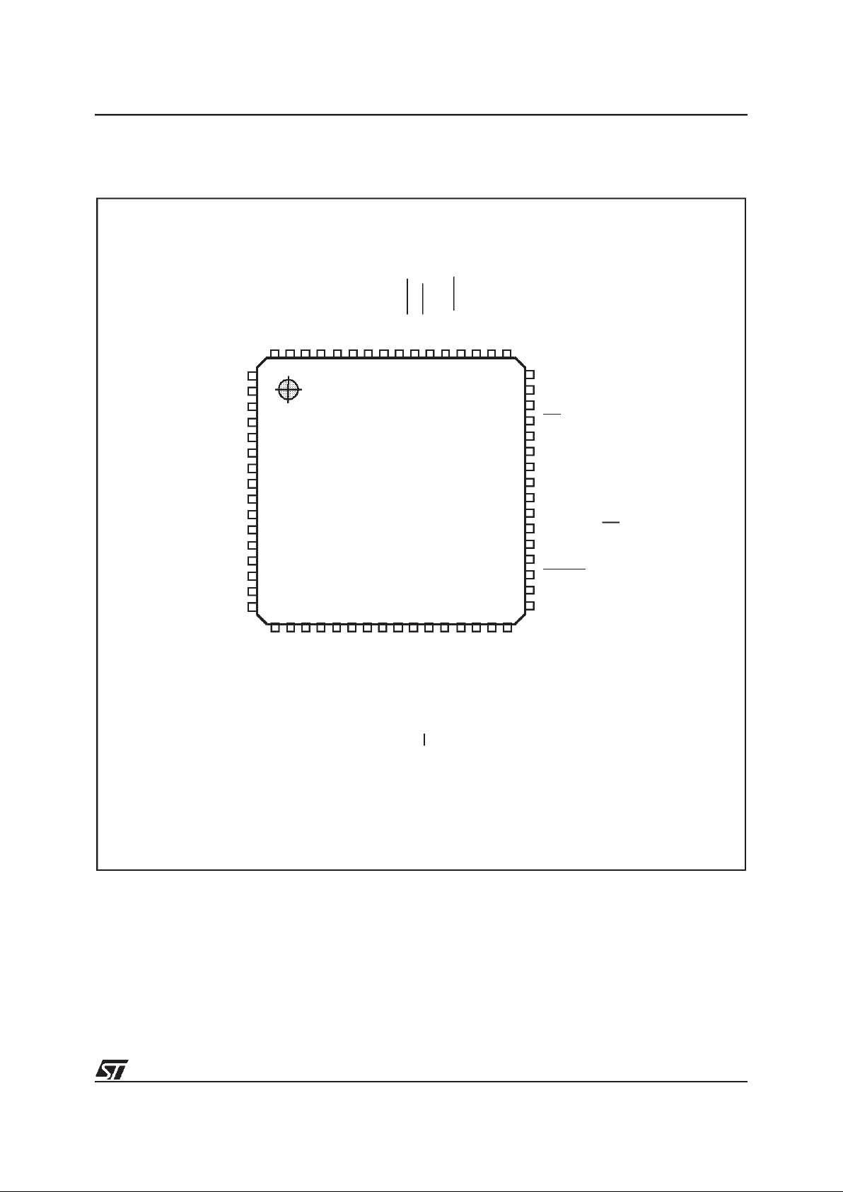
1.2 PIN DESCRIPTION
Figure 3. 64-Pin Package Pin-Out
N.C. = Not connected
WKUP14/A10/P1.2
WKUP14/A9/P1.1
WKUP14/A8/P1.0
D7/A7/P0.7
D6/A6/P0.6
D5/A5/P0.5
D4/A4/P0.4
D3/A3/P0.3
D2/A2/P0.2
D1/A1/P0.1
D0/A0/P0.0
AIN5/P6.7
AIN4/P6.6
USBSOF/AIN3/P6.5
USBSOF/AIN2/P6.4
WKUP13/AIN1/P6.3
P1.3/A11/WKUP14
P1.4/A12/WKUP14
P1.5/A13/WKUP14
P1.6/A14/WKUP14
P1.7/A15/WKUP14
N.C.
N.C.
VSSVDDP4.0/BREQ
P4.1/WAIT
P4.2
P4.3//BACK
USBDM0
USBDP0
N.C.
N.C.
USBVCC
USBGND
DS
P3.0/INT7/SOUT
P3.1/INT7/RTS
P3.2/INT7/TXCLK/CLKOUT
P3.3/INT7/RXCLK
P3.4/INT7/DCD
P3.5/INT7/SIN
P3.6/INT7/AS
P3.7/INT7/SDS
V
PP
RESET
P5.0/INT1/TINA
N.C.
AV
DD
WKUP12/AIN0/INTCLK/P6.2
WKUP11/SCL/EXTRG/INT6/P6.1
WKUP10/SDA/INT5/P6.0
V
DD
OSCIN
V
SS
OSCOUT
WDOUT/NMI/P5.7
WKUP9/TOUTB/P5.6
RW/WDIN/INT0/P5.5
USBOE/WKUP8/P5.4
TOUTA/INT2/P5.3
INT3/P5.2
TINB/INT4/P5.1
N.C.
1
64
16
32
48
16
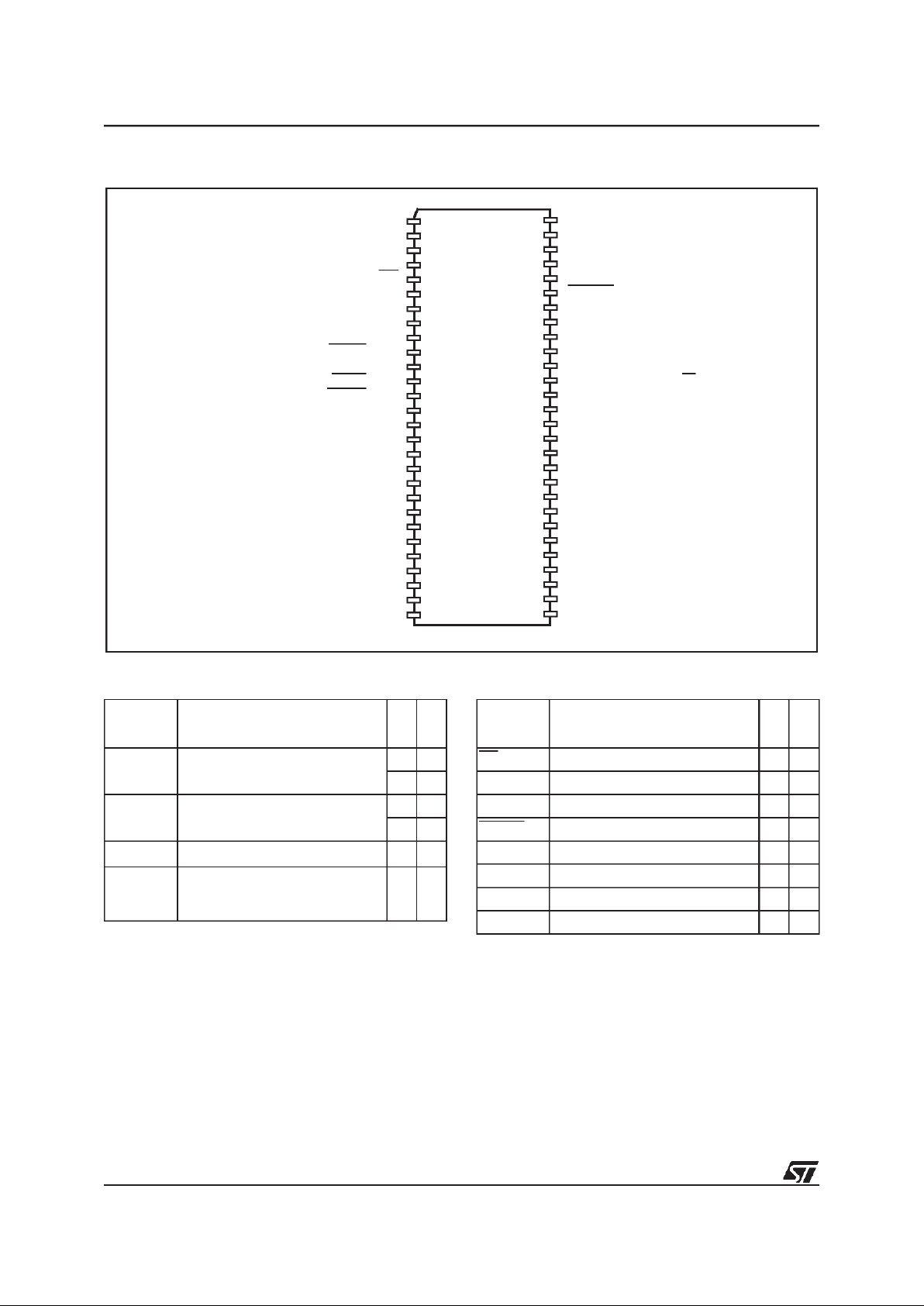
12/224
ST92163 - GENERAL DESCRIPTION
Figure 4. 56-Pin Package Pin-Out
Table 1. Power Supply Pins Table 2. Primary Function pins
156
2928
P3.4/INT7/DCD/WKUP4
P3.5/INT7/SIN/WKUP5
P3.6/INT7/ASN/WKUP6
P3.7/INT7/SDS/WKUP7
V
PP
RESET
P5.0/INT1/TINA
P5.1/INT4/TINB
P5.2/INT3
P5.3/INT2/TOUTA
P5.4/WKUP8/USBOE
P5.5/INT0/WDIN/RW
P5.6/TOUTB/WKUP9
P5.7/NMI/WDOUT
OSCOUT
V
SS
OSCIN
V
DD
P6.0/INT5/SDA/WKUP10
P6.1/INT6/EXTRG/SCL/WKUP11
P6.2/INTCLK/AIN0/WKUP12
AV
DD
P6.3/AIN1/WKUP13
P6.4/AIN2/USBSOF
P6.5/AIN3/USBSOF
P0.0/A0/D0
P0.1/A1/D1
P0.2/A2/D2
WKUP3/RXCLK/INT7/P3.3
WKUP2/CLKOUT/TXCLK/INT7/P3.2
WKUP1/RTS/INT7/P3.1
WKUP0/SOUT/INT7/P3.0
DS
USBGND
USBVCC
USBDP0
USBDM0
BACK/P4.3
P4.2
WAIT/P4.1
BREQ/P4.0
V
DD
V
SS
WKUP14/A15/P1.7
WKUP14/A14/P1.6
WKUP14/A13/P1.5
WKUP14/A12/P1.4
WKUP14/A11/P1.3
WKUP14/A10/P1.2
WKUP14/A9/P1.1
WKUP14/A8/P1.0
D7/A7/P0.7
D6/A6/P0.6
D5/A5/P0.5
D4/A4/P0.4
D3/A3/P0.3
Name Function
DIP56
QFP64
V
DD
Main Power Supply Voltage
(2 pins internally connected)
14 21
39 56
V
SS
Digital Circuit Ground
(2 pins internally connected)
15 23
41 57
AV
DD
Analog Circuit Supply Voltage 35 17
V
PP
EPROM Programming Voltage.
Must be connected to ground in
normal operating mode.
52 36
Name Function
DIP56
QFP64
DS Data Strobe 5 45
OSCIN Oscillator Input 40 22
OSCOUT Oscillator Output 42 24
RESET Reset to initialize the ST9 51 35
USBGND USB bus ground level 6 46
USBVCC USB voltage regulator output 7 47
USBDM0 USB Upstream port Data- line 9 51
USBDP0 USB Upstream port Data+ line 8 50
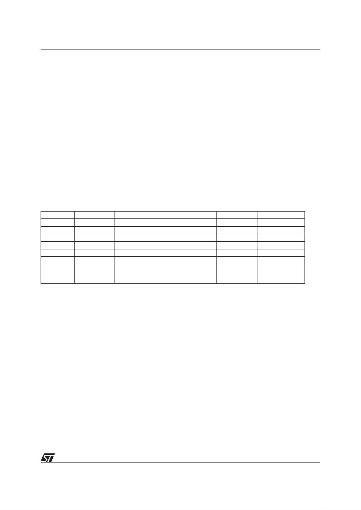
13/224
ST92163 - GENERAL DESCRIPTION
1.3 I/O Port Pins
All the ports of the device can be programmed as
Input/Output or in Input mode, compatible with
TTL or CMOS levels (except where Schmitt Trigger is present). Each bit can be programmed individually (Refer to the I/O ports chapter).
TTL/CMOS Input
For all those port bits where no input schmitt trigger is implemented, it is always possible to program the input level as TTL or CMOS compatible
by programming the relevant PxC2.n control bit.
Refer I/O Ports Chapter to the section titled “Input/
Output Bit Configuration”.
Push-Pull/OD Output
The output buffer can be programmed as pushpull or open-drain: attention must be paid to the
fact thatthe open-drain option correspondsonly to
a disabling of P-channel MOS transistor of the
buffer itself: it is still present and physically connected to thepin. Consequentlyit isnot possible to
increase the output voltage on the pin over
VDD+0.3 Volt, to avoid direct junction biasing.
Pure Open-drain Output
The user can increase the voltage on an I/O pin
over VDD+0.3 Volt where theP-channel MOStransistor is physically absent: this is allowed on all
“Pure Open Drain” pins. Of course, in this case the
push-pull option is not available and any weak
pull-up must implemented externally.
Table 3. I/O Port Characteristics
Legend: WPU = Weak Pull-Up, OD = Open Drain
Input Output Weak Pull-Up Reset State
Port 0[7:0] TTL/CMOS Push-Pull/OD Yes Bidirectional WPU
Port 1[7:0] TTL/CMOS Push-Pull/OD Yes Bidirectional WPU
Port 3[7:0] Schmitt trigger Push-Pull/OD Yes Bidirectional WPU
Port 4[3:0] Schmitt trigger Push-Pull/OD Yes Bidirectional WPU
Port 5[7:0] Schmitt trigger Push-Pull/OD Yes Bidirectional WPU
Port 6[1:0]
Port 6[5:2]
Port 6.6
Port 6.7
Schmitt trigger
TTL/CMOS
Schmitt trigger
TTL/CMOS
Pure Open Drain with high sink capability
Push-Pull/OD with high sink capability
Push-Pull/OD with high sink capability
Push-Pull/OD with high sink capability
No
Yes
No
No
Bidirectional
Bidirectional WPU
Bidirectional
Bidirectional

14/224
ST92163 - GENERAL DESCRIPTION
Table 4. ST92163 Alternate Functions
Port
Name
General
Purpose I/O
Pin
No.
Alternate Functions
DIP56
QFP64
P0.0
All ports useable
for general purpose I/O (input,
output or bidirectional)
31 11 A0/D0 I/O Ext. Mem. Address/Data bit 0
P0.1 30 10 A1/D1 I/O Ext. Mem. Address/Data bit 1
P0.2 29 9 A2/D2 I/O Ext. Mem. Address/Data bit 2
P0.3 28 8 A3/D3 I/O Ext. Mem. Address/Data bit 3
P0.4 27 7 A4/D4 I/O Ext. Mem. Address/Data bit 4
P0.5 26 6 A5/D5 I/O Ext. Mem. Address/Data bit 5
P0.6 25 5 A6/D6 I/O Ext. Mem. Address/Data bit 6
P0.7 24 4 A7/D7 I/O Ext. Mem. Address/Data bit 7
P1.0 23 3
A8 I/O Ext. Mem. Address bit 8
WKUP14 I Wakeup Line 14 (***)
P1.1 22 2
A9 I/O Ext. Mem. Address bit 9
WKUP14 I Wakeup Line 14 (***)
P1.2 21 1
A10 I/O Ext. Mem. Address bit 10
WKUP14 I Wakeup Line 14 (***)
P1.3 20 64
A11 I/O Ext. Mem. Address bit 11
WKUP14 I Wakeup Line 14 (***)
P1.4 19 63
A12 I/O Ext. Mem. Address bit 12
WKUP14 I Wakeup Line 14 (***)
P1.5 18 62
A13 I/O Ext. Mem. Address bit 13
WKUP14 I Wakeup Line 14 (***)
P1.6 17 61
A14 I/O Ext. Mem. Address bit 14
WKUP14 I Wakeup Line 14 (***)
P1.7 16 60
A15 I/O Ext. Mem. Address bit 15
WKUP14 I Wakeup Line 14 (***)
P3.0 4 44
WKUP0 I Wakeup Line 0
INT7 I External Interrupt 7 (*)
SOUT O SCI Data Output
P3.1 3 43
WKUP1 O Wakeup Line 1
INT7 I External Interrupt 7 (*)
RTS O SCI Request to Send

15/224
ST92163 - GENERAL DESCRIPTION
P3.2
All ports useable
for general purpose I/O (input,
output or bidirec-
tional)
242
WKUP2 I Wakeup Line 2
INT7 I External Interrupt 7 (*)
TXCLK I SCI Transmit CK Input
CLKOUT O SCI Clock Output
P3.3 1 41
WKUP3 I Wakeup Line 3
INT7 I External Interrupt 7 (*)
RXCLK I SCI Receive CK Input
O
P3.4 56 40
WKUP4 I Wakeup Line 4
INT7 I External Interrupt 7 (*)
DCD I SCI Data Carrier Detect
O
P3.5 55 39
WKUP5 I Wakeup Line 5
INT7 I External Interrupt 7 (*)
SIN I SCI Data Input
O
P3.6 54 38
WKUP6 I Wakeup Line 6
INT7 I External Interrupt 7 (*)
AS (**) O Ext. Mem. Address Strobe
P3.7 53 37
WKUP7 I Wakeup Line 7
INT7 I External Interrupt 7 (*)
SDS O SCI Synchronous Data Send
P4.0 13 55 BREQ I Ext. Mem. Bus Request
P4.1 12 54
WAIT I Ext. Mem. Wait Input
RW O Ext. Mem. Read/Write Mode Select
P4.2 11 53
I
AS (**) O Ext. Mem. Address Strobe
P4.3 10 52
I
BACK O Ext. Mem. bus acknow
Port
Name
General
Purpose I/O
Pin
No.
Alternate Functions
DIP56
QFP64
16/224
ST92163 - GENERAL DESCRIPTION
P5.0
All ports useable
for general purpose I/O (input,
output or bidirectional)
50 34
INT1 I External Interrupt 1
TINA I MF Timer Input A
O
P5.1 49 31
INT4 I External Interrupt 4
TINB I MF Timer Input B
O
P5.2 48 30 INT3 I External Interrupt 3
P5.3 47 29
INT2 I External Interrupt 2
TOUTA O MF Timer Output A
P5.4 46 28
WKUP8 I Wakeup Line 8
USBOE O USB Outputenable
P5.5 45 27
WDIN I Watchdog TimerInput
INT0 I External Interrupt 0
RW O Ext. Mem. Read/Write Mode Select
P5.6 44 26
WKUP9 I Wakeup Line 9
TOUTB O MF Timer Output B
P5.7 43 25
NMI I Non Maskable Interrupt
WDOUT O Watchdog Timer Output
P6.0 38 20
WKUP10 I Wakeup Line 10
INT5 I External Interrupt 5
SDAI I I
2
C Bus Data In
SDAO O I
2
C Bus Data Out
P6.1 37 19
WKUP11 I Wakeup Line 11
INT6 I External Interrupt 6
SCLI I I
2
C Bus Clock In
EXTRG I A/D External Trigger
SCLO O I
2
C Bus Clock Out
P6.2 36 18
AIN0 I A/D Analog Input 0
WKUP12 I Wakeup Line 12
INTCLK O Internal Clock
P6.3 34 16
WKUP13 I Wakeup Line 13
AIN1 I A/D Analog Input 1
O
Port
Name
General
Purpose I/O
Pin
No.
Alternate Functions
DIP56
QFP64
17/224
ST92163 - GENERAL DESCRIPTION
*Eight interrupt lines internally connected to INT7
through a boolean AND function.
** AS cannot be disabled by software if the ASAF
bit is set (Page Register 245) once the corresponding P3.6 bit is configured as an Alternate
Function output.
***Eight wakeup lines internally connected to
WKUP14 through a boolean AND function.
Note: The reset state of Port 0 and Port 1 is Input,
Weak Pull-Up. To interface external memory, the
ports must be configured by software as alternate
function output.
P6.4
All ports useable
for general purpose I/O (input,
output or bidirectional)
33 15
AIN2 I A/D Analog Input 2
USBSOF O USB SOFSynchro
P6.5 32 14 AIN3 I A/D Analog Input 3
USBSOF O USB SOFSynchro
P6.6 - 13
AIN4 I A/D Analog Input 4
O
P6.7 - 12
AIN5 I A/D Analog Input 5
O
Port
Name
General
Purpose I/O
Pin
No.
Alternate Functions
DIP56
QFP64

18/224
ST92163 - GENERAL DESCRIPTION
How to configure the I/O ports
To configure the I/O ports, use the information in
Table 3 and Table 4 and the Port Bit Configuration
Table in the I/O Ports Chapter on page 100.
I/O Note = the hardware characteristics fixed for
each port line.
Inputs:
– If I/O note= TTL/CMOS, either TTL or CMOS in-
put level can be selected by software.
– If I/O note = Schmitt trigger, selecting CMOS or
TTL inputby software hasno effect, the inputwill
always be Schmitt Trigger.
Outputs:
– If I/O note= Push-Pull, either Push Pull or Open
Drain can be selectedby software.
– If I/O note = Open Drain, selecting Push-Pull by
software has no effect, the input will always be
Open Drain.
Alternate Functions (AF) = More than one AF
cannot be assigned to an external pin at the same
time: it can be selected as follows, but simultaneous availability of several functions of one pin is
obviously impossible.
AF Inputs:
– AF is selected implicitly by enablingthe corre-
sponding peripheral. Exceptions tothis areADC
inputs which are selected explicitly as AF bysoft-
ware.
AF Outputs or Bidirectional Lines:
– In the case of Outputs or I/Os, AF is selected
explicitly by software.
Example 1: Timer/Watchdog input
AF: WDIN, Port: P5.5, I/O note: InputSchmitt Trigger.
Write the port configuration bits:
P5C2.5=1
P5C1.5=0
P5C0.5=1
Enable the WDT peripheral by software as de-
scribed in the WDT chapter.
Example 2: Timer/Watchdog output
AF: WDOUT, Port: P5.7, I/O note: None
Write the port configuration bits:
P5C2.7=0
P5C1.7=1
P5C0.7=1
Example 3: ADC input
AF: AIN0, Port: P6.2, I/O note: Does not apply to
ADC
Write the port configuration bits:
P6C2.2=1
P6C1.2=1
P6C0.2=1
19/224
ST92163 - GENERAL DESCRIPTION
1.4 MEMORY MAP
Figure 5. ST92163 Memory Map
SEGMENT 20h
64 Kbytes
200000h
21FFFFh
20C000h
20BFFFh
208000h
207FFFh
204000h
203FFFh
PAGE 80 - 16 Kbytes
PAGE 81 - 16 Kbytes
PAGE 82 - 16 Kbytes
PAGE 83 - 16 Kbytes
20F800h
20FFFFh
Note: Internal RAM addresses are
RAM
2 Kbytes
Reserved
Internal
External
Memory
Reserved
External
Memory
SEGMENT 21h
64 Kbytes
Internal ROM/EPROM
20FFFFh
220000h
3FFFFFh
repeated each 2 Kbytes inside segment 20h.
Lower Memory
(usually external ROM/EPROM
Upper Memory
(usually external RAM mapped
210000h
Note: The total amount of external memory is 64 Kbytes.
mapped in Segment 1)
in Segment 23h)
1FFFFFh
010000h
00FFFFh
00C000h
00BFFFh
008000h
007FFFh
004000h
000000h
003FFFh
PAGE 0 - 16 Kbytes
PAGE 1 - 16 Kbytes
PAGE 2 - 16 Kbytes
PAGE 3 - 16 Kbytes
64 Kbytes
SEGMENT 0
000000h
004FFFh
ROM/EPROM
20 Kbytes
Internal

20/224
ST92163 - GENERAL DESCRIPTION
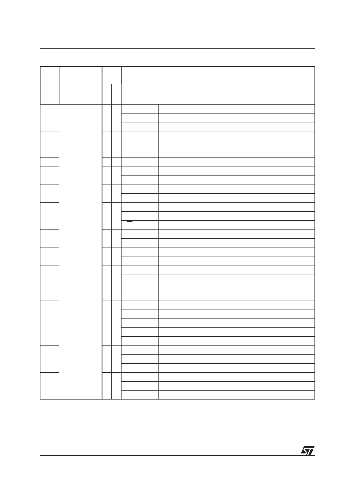
1.5 ST92163 REGISTER MAP
Table 6 contains themap of thegroup Fperipheral
pages.
The common registers used by each peripheral
are listed in Table 5.
Be very careful to correctly program both:
– The set of registersdedicated to a particular
function or peripheral.
– Registers common to other functions.
– In particular, double-check that any registers
with “undefined” resetvalues have been correct-
ly initialized.
Warning: Notethat in the EIVR and each IVR reg-
ister, all bits are significant. Take care when defining base vector addresses that entriesin theInterrupt Vector table do not overlap.
Table 5. Common Registers
Figure 6. ST92163 Register Groups
Function or Peripheral Common Registers
SCI, MFT CICR + NICR + DMA REGISTERS+ I/O PORT REGISTERS
ADC CICR + NICR + I/O PORT REGISTERS
WDT
CICR + NICR + EXTERNAL INTERRUPT REGISTERS +
I/O PORT REGISTERS
I/O PORTS I/O PORT REGISTERS + MODER
EXTERNAL INTERRUPT INTERRUPT REGISTERS + I/O PORT REGISTERS
RCCU INTERRUPT REGISTERS + MODER
REGISTER FILE
SYSTEM REGISTERS
255
240
239
224
223
F
E
D
C
B
A
9
8
7
6
5
4
3
2
1
0
15
00
PAGED REGISTERS
These register groups (16 registers per group)
The amount of reserved registers depends on
the number of endpoints used in the program.
(8 registers are used per endpoint).
for USB DMA.are potentially reserved

21/224
ST92163 - GENERAL DESCRIPTION
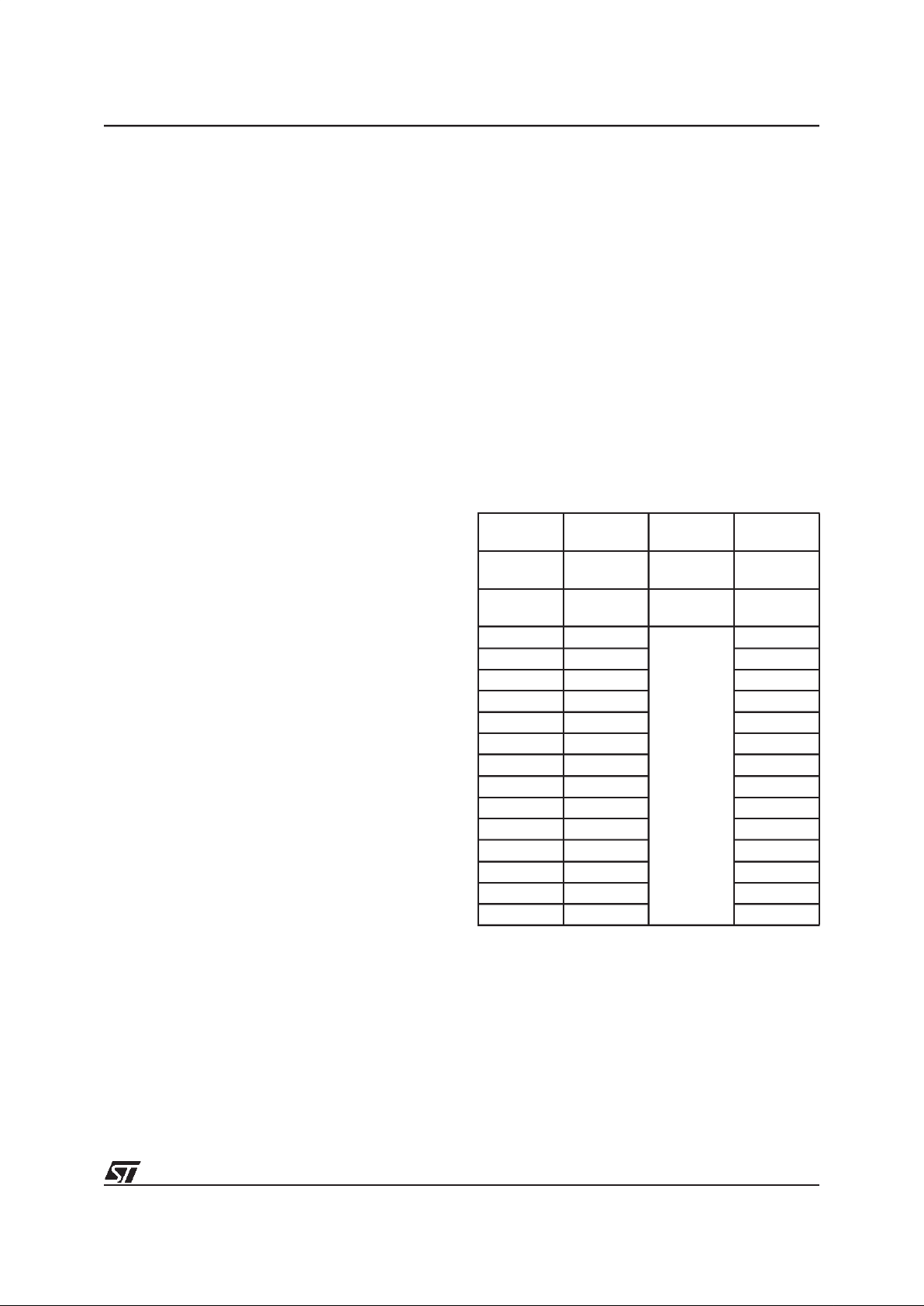
Table 6. Group F Pages Register Map
Resources available on the ST92163 device:
Register
Page
0 2 3 4 5 9 101520212443555762
R255
Res.
Res.
Res.
USB
Endpoints
Res.
MFT
USB
Com-
mon
I2C MMU SCI
Port
9
Res.
WUI
MU
ADC
R254
Port
3
R253
R252 WCR
R251
WDT
Res.
Port
6
Port
8
R250
R249
R248
Res.
R247
EXT
INT
Res.
Res.
R246
Port
5
RCCU
R245
R244
R243 Res.
MFT
R242
Port
4
R241
Res.
R240
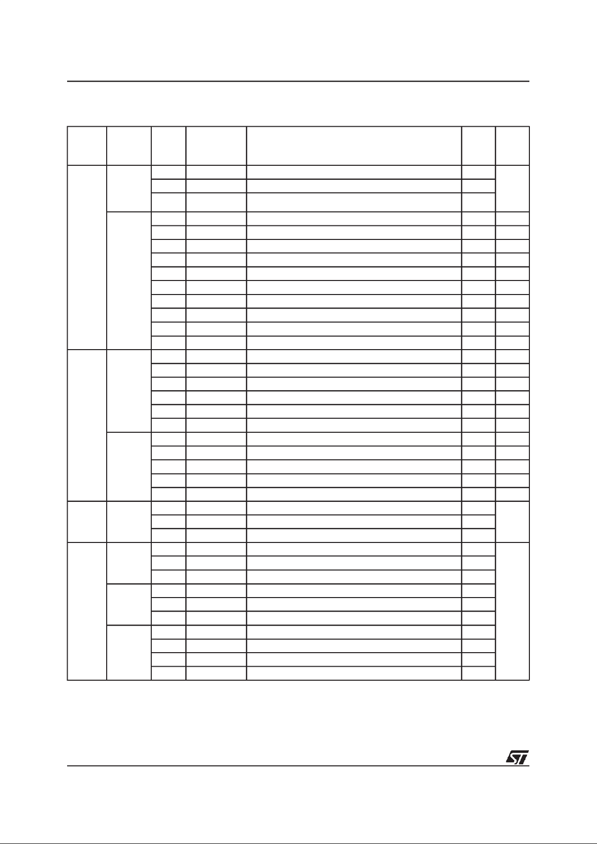
22/224
ST92163 - GENERAL DESCRIPTION
Table 7. Detailed Register Map
Page
No.
Block
Reg.
No.
Register
Name
Description
Reset
Value
Hex.
Doc.
Page
System
I/O
Port
3:5
R227 P3DR Port 3 Data Register FF
98
R228 P4DR Port 4 Data Register FF
R229 P5DR Port 5 Data Register FF
Core
R230 CICR Central Interrupt Control Register 87 30
R231 FLAGR Flag Register 00 31
R232 RP0 Pointer 0 Register 00 33
R233 RP1 Pointer 1 Register 00 33
R234 PPR Page Pointer Register 54 35
R235 MODER Mode Register E0 35
R236 USPHR User Stack Pointer High Register xx 37
R237 USPLR User Stack Pointer Low Register xx 37
R238 SSPHR System Stack Pointer High Reg. xx 37
R239 SSPLR System Stack Pointer Low Reg. xx 37
0
INT
R242 EITR External Interrupt Trigger Register 00 59
R243 EIPR External Interrupt Pending Reg. 00 60
R244 EIMR External Interrupt Mask-bit Reg. 00 60
R245 EIPLR External Interrupt Priority Level Reg. FF 60
R246 EIVR External Interrupt Vector Register x6 61
R247 NICR Nested Interrupt Control 00 61
WDT
R248 WDTHR Watchdog Timer High Register FF 109
R249 WDTLR Watchdog Timer Low Register FF 109
R250 WDTPR Watchdog Timer Prescaler Reg. FF 109
R251 WDTCR Watchdog Timer Control Register 12 109
R252 WCR Wait Control Register 7F 110
2
I/O
Port
3
R252 P3C0 Port 3 Configuration Register 0 00
98R253 P3C1 Port 3 Configuration Register 1 00
R254 P3C2 Port 3 Configuration Register 2 00
3
I/O
Port
4
R240 P4C0 Port 4 Configuration Register 0 00
98
R241 P4C1 Port 4 Configuration Register 1 00
R242 P4C2 Port 4 Configuration Register 2 00
I/O
Port
5
R244 P5C0 Port 5 Configuration Register 0 00
R245 P5C1 Port 5 Configuration Register 1 00
R246 P5C2 Port 5 Configuration Register 2 00
I/O
Port
6
R248 P6C0 Port 6 Configuration Register 0 00
R249 P6C1 Port 6 Configuration Register 1 00
R250 P6C2 Port 6 Configuration Register 2 00
R251 P6DR Port 6 Data Register FF
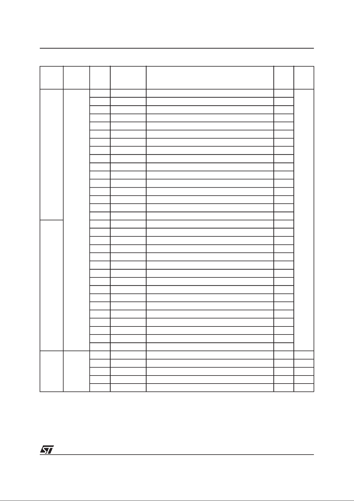
23/224
ST92163 - GENERAL DESCRIPTION
4
USB
End
Points
R240 EP0RA Endpoint 0 Register A (Transmission) 00
143
R241 EP0RB Endpoint 0 Register B (Reception) 00
R242 EP1RA Endpoint 1 Register A (Transmission) 00
R243 EP1RB Endpoint 1 Register B (Reception) 00
R244 EP2RA Endpoint 2 Register A (Transmission) 00
R245 EP2RB Endpoint 2 Register B (Reception) 00
R246 EP3RA Endpoint 3 Register A (Transmission) 00
R247 EP3RB Endpoint 3 Register B (Reception) 00
R248 EP4RA Endpoint 4 Register A (Transmission) 00
R249 EP4RB Endpoint 4 Register B (Reception) 00
R250 EP5RA Endpoint 5 Register A (Transmission) 00
R251 EP5RB Endpoint 5 Register B (Reception) 00
R252 EP6RA Endpoint 6 Register A (Transmission) 00
R253 EP6RB Endpoint 6 Register B (Reception) 00
R254 EP7RA Endpoint 7 Register A (Transmission) 00
R255 EP7RB Endpoint 7 Register B (Reception) 00
5
R240 EP8RA Endpoint 8 Register A (Transmission) 00
R241 EP8RB Endpoint 8 Register B (Reception) 00
R242 EP9RA Endpoint 9 Register A (Transmission) 00
R243 EP9RB Endpoint 9 Register B (Reception) 00
R244 EP10RA Endpoint 10 Register A (Transmission) 00
R245 EP10RB Endpoint 10 Register B (Reception) 00
R246 EP11RA Endpoint 11 Register A (Transmission) 00
R247 EP11RB Endpoint 11 Register B (Reception) 00
R248 EP12RA Endpoint 12 Register A (Transmission) 00
R249 EP12RB Endpoint 12 Register B (Reception) 00
R250 EP13RA Endpoint 13 Register A (Transmission) 00
R251 EP13RB Endpoint 13 Register B (Reception) 00
R252 EP14RA Endpoint 14 Register A (Transmission) 00
R253 EP14RB Endpoint 14 Register B (Reception) 00
R254 EP15RA Endpoint 15 Register A (Transmission) 00
R255 EP15RB Endpoint 15 Register B (Reception) 00
9 MFT
R240 DCPR DMA Counter Pointer Register xx 132
R241 DAPR DMA Address Pointer Register xx 133
R242 T_IVR Interrupt Vector Register xx 133
R243 IDCR Interrupt/DMA Control Register C7 134
R248 IOCR I/O Connection Register FC 134
Page
No.
Block
Reg.
No.
Register
Name
Description
Reset
Value
Hex.
Doc.
Page
24/224
ST92163 - GENERAL DESCRIPTION
10 MFT
R240 REG0HR Capture Load Register 0 High xx 125
R241 REG0LR Capture Load Register 0 Low xx 125
R242 REG1HR Capture Load Register 1 High xx 125
R243 REG1LR Capture Load Register 1 Low xx 125
R244 CMP0HR Compare 0 Register High 00 125
R245 CMP0LR Compare 0 Register Low 00 125
R246 CMP1HR Compare 1 Register High 00 125
R247 CMP1LR Compare 1 Register Low 00 125
R248 TCR Timer Control Register 0x 126
R249 TMR Timer Mode Register 00 127
R250 T_ICR External Input Control Register 0x 128
R251 PRSR Prescaler Register 00 128
R252 OACR Output A Control Register xx 129
R253 OBCR Output B Control Register xx 130
R254 T_FLAGR Flags Register 00 31
R255 IDMR Interrupt/DMA MaskRegister 00 132
15
USB
Common
R240 DADDR0 Device Address Register 0 00
143
R241 DADDR1 Device Address Register 1 00
R242 DADDR2 Device Address Register 2 00
R243 DADDR3 Device Address Register 3 00
R244 DADDR4 Device Address Register 4 00
R245 DADDR5 Device Address Register 5 00
R246 DADDR6 Device Address Register 6 00
R247 DADDR7 Device Address Register 7 00
R248 USBIVR USB Interrupt Vector Register xx 139
R249 USBISTR USB Interrupt Status Register 00 139
R250 USBIMR USB Interrupt Mask Register 00 140
R251 USBIPR USB Interrupt Priority Register xx 140
R252 USBCTLR USB Control Register 17 141
R253 CTRINF CTR Interrrupt Flags xx 142
R254 FNRH Frame Number Register High 0x 142
R255 FNRL Frame Number Register Low xx 142
Page
No.
Block
Reg.
No.
Register
Name
Description
Reset
Value
Hex.
Doc.
Page
25/224
ST92163 - GENERAL DESCRIPTION
20 I2C
R240 I2CCR I
2
C Control Register 00 186
R241 I2CSR1 I
2
C Status Register 1 00 187
R242 I2CSR2 I
2
C Status Register 2 00 189
R243 I2CCCR I
2
C Clock Control Register 00 190
R244 I2COAR1 I
2
C Own Address Register 1 00 190
R245 I2COAR2 I
2
C Own Address Register 2 00 191
R246 I2CDR I
2
C Data Register 00 191
R247 I2CADR I
2
C General Call Address A0 191
R248 I2CISR I
2
C Interrupt Status Register xx 192
R249 I2CIVR I
2
C Interrupt Vector Register xx 193
R250 I2CRDAP Receiver DMA Source Addr. Pointer xx 193
R251 I2CRDC Receiver DMA Transaction Counter xx 193
R252 I2CTDAP Transmitter DMA Source Addr. Pointer xx 194
R253 I2CTDC Transmitter DMA Transaction Counter xx 194
R254 I2CECCR I
2
C Extended Clock Control Register 00 194
R255 I2CIMR I
2
C Interrupt Mask Register x0 195
21
MMU
R240 DPR0 Data Page Register 0 00 42
R241 DPR1 Data Page Register 1 01 42
R242 DPR2 Data Page Register 2 02 42
R243 DPR3 Data Page Register 3 83 42
R244 CSR Code Segment Register 00 43
R248 ISR Interrupt Segment Register x0 43
R249 DMASR DMA Segment Register x0 43
EXTMI
R245 EMR1 External Memory Register 1 80 95
R246 EMR2 External Memory Register 2 0F 96
24 SCI
R240 RDCPR Receiver DMA Transaction Counter Pointer xx 165
R241 RDAPR Receiver DMA Source Address Pointer xx 165
R242 TDCPR Transmitter DMA Transaction Counter Pointer xx 165
R243 TDAPR Transmitter DMADestination Address Pointer xx 165
R244 S_IVR Interrupt Vector Register xx 166
R245 ACR Address/Data Compare Register xx 166
R246 IMR Interrupt Mask Register x0 167
R247 S_ISR Interrupt Status Register xx 43
R248 RXBR Receive Buffer Register xx 169
R248 TXBR Transmitter Buffer Register xx 169
R249 IDPR Interrupt/DMA Priority Register xx 170
R250 CHCR Character Configuration Register xx 171
R251 CCR Clock Configuration Register 00 172
R252 BRGHR Baud Rate Generator High Reg. xx 173
R253 BRGLR Baud Rate Generator Low Register xx 173
R254 SICR Synchronous Input Control 03 173
R255 SOCR Synchronous Output Control 01 174
Page
No.
Block
Reg.
No.
Register
Name
Description
Reset
Value
Hex.
Doc.
Page
26/224
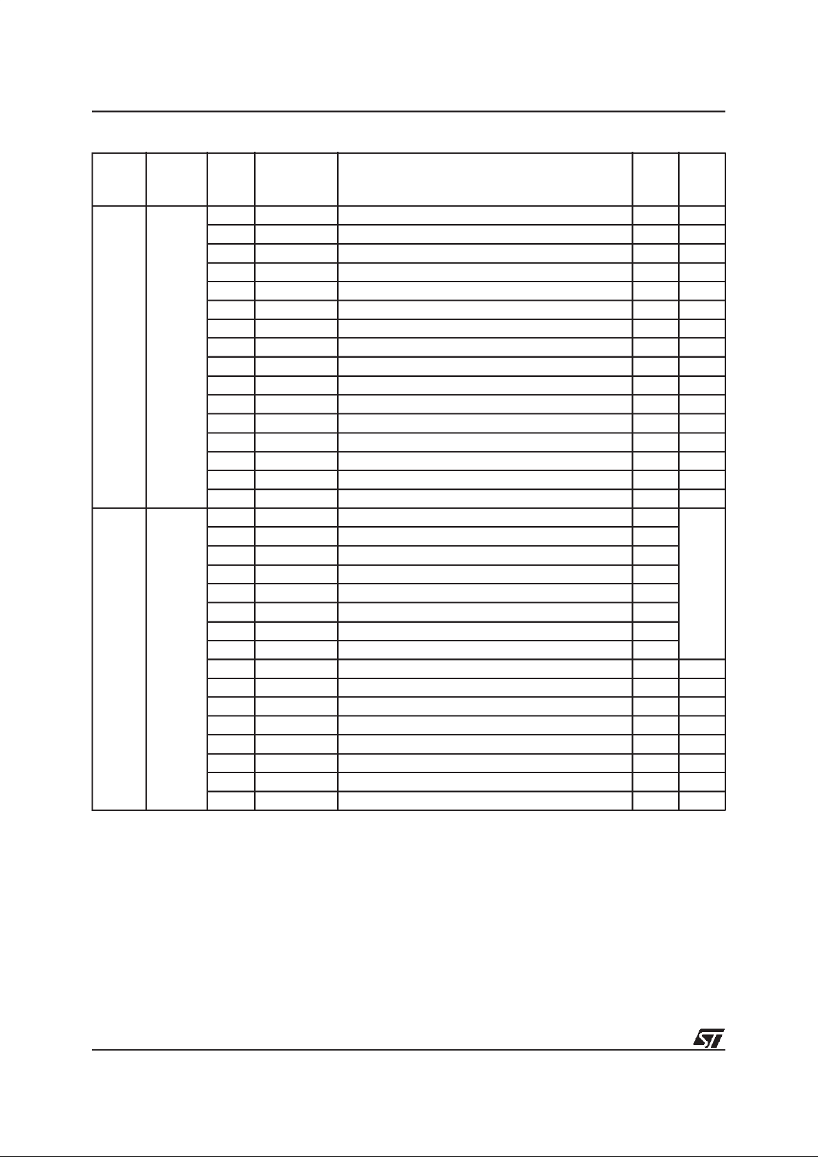
ST92163 - GENERAL DESCRIPTION
Note: xx denotes a byte with an undefined value, but some bits may have defined values. See register description for de-
tails.
43
I/O
Port
8
R248 P8C0 Port 8 Configuration Register 0 00
98
R249 P8C1 Port 8 Configuration Register 1 00
R250 P8C2 Port 8 Configuration Register 2 00
R251 P8DR Port 8 Data Register FF
I/O
Port
9
R252 P9C0 Port 9 Configuration Register 0 00
R253 P9C1 Port 9 Configuration Register 1 00
R254 P9C2 Port 9 Configuration Register 2 00
R255 P9DR Port 9 Data Register FF
55 RCCU
R240 CLKCTL Clock Control Register 00 81
R242 CLK_FLAG Clock Flag Register
48, 28
or 08
82
R246 PLLCONF PLL Configuration Register xx 83
59 WUIMU
R249 WUCTRL Wake-Up Control Register 00 67
R250 WUMRH Wake-Up Mask Register High 00 68
R251 WUMRL Wake-Up Mask Register Low 00 68
R252 WUTRH Wake-Up Trigger Register High 00 69
R253 WUTRL Wake-Up Trigger Register Low 00 69
R254 WUPRH Wake-Up Pending Register High 00 69
R255 WUPRL Wake-Up Pending Register Low 00 69
60 USB
R244 DEVCONF1 USB device configuration 1 0F 146
R245 DEVCONF2 USB device configuration 2 00 146
R246 MIRRA Mirror Register A xx 147
R247 MIRRB Mirror Register B xx 147
62 ADC
R240 ADDTR Channel i Data Register xx 199
R241 ADCLR Control Logic Register 00 199
R242 ADINT AD Interrupt Register 01 200
Page
No.
Block
Reg.
No.
Register
Name
Description
Reset
Value
Hex.
Doc.
Page
27/224
ST92163 - DEVICE ARCHITECTURE
2 DEVICE ARCHITECTURE
2.1 CORE ARCHITECTURE
The ST9+ Core or Central Processing Unit (CPU)
features ahighly optimised instructionset, capable
of handling bit, byte (8-bit) and word (16-bit) data,
as well as BCDand Boolean formats; 14 addressing modes are available.
Four independent buses are controlled by the
Core: a 16-bit Memory bus, an 8-bit Register data
bus, an 8-bit Register address bus and a 6-bit Interrupt/DMA bus which connects the interrupt and
DMA controllersin theon-chip peripherals with the
Core.
This multiple bus architecture affords a high degree ofpipeliningand parallel operation, thus making the ST9+ family devices highly efficient, both
for numerical calculation, data handling and with
regard to communication with on-chip peripheral
resources.
2.2 MEMORY SPACES
There are two separate memory spaces:
– The Register File, which comprises 240 8-bit
registers, arranged as 15 groups (Group 0 to E),
each containing sixteen 8-bit registers plus up to
64 pages of 16 registers mapped in Group F,
which hold data and control bits for the on-chip
peripherals and I/Os.
– A single linear memory space accommodating
both program anddata. Allof the physically separate memoryareas, including the internal ROM,
internal RAM and external memory are mapped
in this common address space. The total addressable memory space of 4 Mbytes(limited by
the size of on-chip memory and the number of
external address pins) is arranged as 64 segments of 64 Kbytes. Each segment is further
subdivided into four pages of 16 Kbytes, as illustrated in Figure 1. A Memory Management Unit
uses aset of pointer registers to address a 22-bit
memory field using 16-bit address-based instructions.
2.2.1 Register File
The Register File consists of (see Figure 2):
– 224 general purpose registers (Group 0 to D,
registers R0 to R223)
– 6 system registers in the System Group (Group
E, registers R224 to R239)
– Up to 64 pages, depending on device configura-
tion, each containing up to 16 registers, mapped
to Group F (R240 to R255), see Figure 3.
Figure 7. Single Program and Data Memory Address Space
3FFFFFh
3F0000h
3EFFFFh
3E0000h
20FFFFh
02FFFFh
020000h
01FFFFh
010000h
00FFFFh
000000h
8
7
6
5
4
3
2
1
0
63
62
2
1
0
Address 16K Pages 64K Segments
up to 4 Mbytes
Data
Code
255
254
253
252
251
250
249
248
247
9
10
11
21FFFFh
210000h
133
134
135
33
Reserved
132
28/224
ST92163 - DEVICE ARCHITECTURE
MEMORY SPACES (Cont’d)
Figure 8. Register Groups Figure 9. Page Pointer for Group F mapping
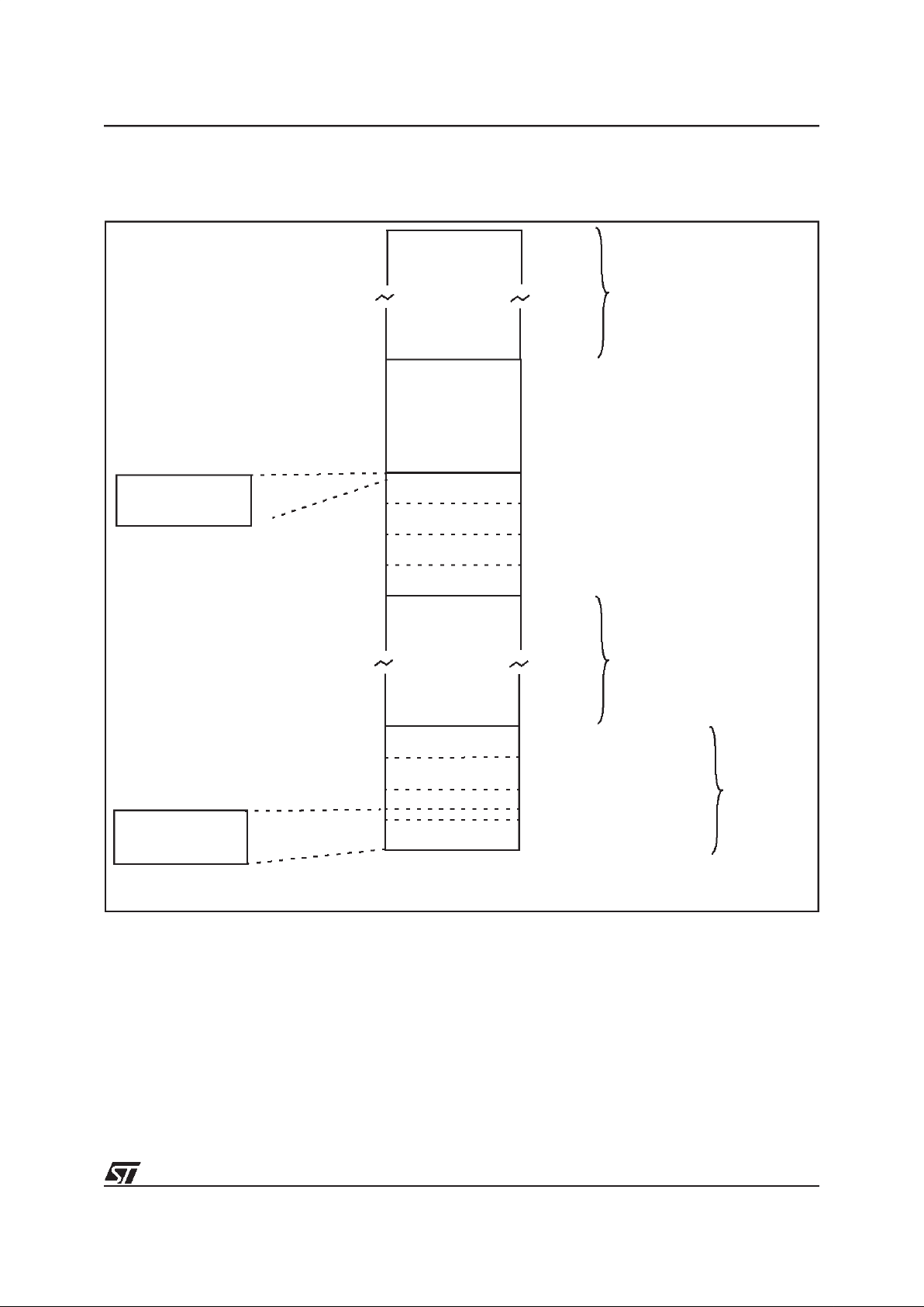
Figure 10. Addressing the Register File
F
E
D
C
B
A
9
8
7
6
5
4
3
PAGED REGISTERS
SYSTEM REGISTERS
2
1
0
00
15
255
240
239
224
223
VA00432
UP TO
64 PAGES
GENERAL
REGISTERS
PURPOSE
224
PAGE 63
PAGE 5
PAGE 0
PAGE POINTER
R255
R240
R224
R0 VA00433
R234
REGISTERFILE
SYSTEM REGISTERS
GROUP D
GROUP B
GROUP C
(1100)
(0011)
R192
R207
255
240
239
224
223
F
E
D
C
B
A
9
8
7
6
5
4
3
2
1
0
15
VR000118
00
R195
R195
(R0C3h)
PAGED REGISTERS
29/224
ST92163 - DEVICE ARCHITECTURE
MEMORY SPACES (Cont’d)
2.2.2 Register Addressing
Register File registers, including Group F paged
registers (but excluding Group D), may be addressed explicitly by means of a decimal, hexadecimal or binary address; thus R231, RE7h and
R11100111b represent the same register (see
Figure 4). Group D registers can only be addressed in Working Register mode.
Note that an upper case “R” is used to denote this
direct addressing mode.
Working Registers
Certain types of instruction require that registers
be specified in the form “rx”, where x is in the
range 0 to 15:these are known as Working Registers.
Note thata lower case “r” isused to denotethisindirect addressing mode.
Two addressing schemes are available: a single
group of 16 working registers, or two separately
mapped groups, each consisting of 8 working registers. These groups may be mapped starting at
any 8 or 16 byte boundary in the register file by
means of dedicated pointer registers. This technique is described in more detail in Section 1.3.3,
and illustrated in Figure 5 and in Figure 6.
System Registers
The 16 registers in Group E (R224 to R239) are
System registersand maybe addressed usingany
of the register addressing modes. These registers
are described in greater detail in Section 1.3.
Paged Registers
Up to 64 pages, each containing 16 registers, may
be mapped to Group F. These are addressed using any register addressing mode, in conjunction
with the Page Pointer register, R234, which is one
of the System registers. This register selects the
page to be mapped to Group F and, once set,
does not need to be changedif two or more registers on the same pageare to be addressed in succession.
Therefore ifthe PagePointer, R234, is set to5, the
instructions:
spp #5
ld R242, r4
will loadthe contents of working registerr4 into the
third register of page 5 (R242).
These paged registers hold dataand control information relating to the on-chip peripherals, each
peripheral always being associated with the same
pages and registers to ensure code compatibility
between ST9+ devices. The number of these registers therefore depends on the peripherals which
are present in the specific ST9+ family device. In
other words, pages only exist if the relevant peripheral is present.
Table 8. Register File Organization
Hex.
Address
Decimal
Address
Function
Register
File Group
F0-FF 240-255
Paged
Registers
Group F
E0-EF 224-239
System
Registers
Group E
D0-DF 208-223
General
Purpose
Registers
Group D
C0-CF 192-207 Group C
B0-BF 176-191 Group B
A0-AF 160-175 Group A
90-9F 144-159 Group 9
80-8F 128-143 Group 8
70-7F 112-127 Group 7
60-6F 96-111 Group 6
50-5F 80-95 Group 5
40-4F 64-79 Group 4
30-3F 48-63 Group 3
20-2F 32-47 Group 2
10-1F 16-31 Group 1
00-0F 00-15 Group 0
30/224
ST92163 - DEVICE ARCHITECTURE
2.3 SYSTEM REGISTERS
The System registers are listed in Table 2 System
Registers (Group E). They are used to perform all
the importantsystem settings. Their purpose is described inthe following pages. Referto the chapter
dealing with I/O for a description of the PORT[5:0]
Data registers.
Table 9. System Registers (Group E)
2.3.1 Central Interrupt Control Register
Please referto the ”INTERRUPT”chapter for adetailed description of the ST9 interruptphilosophy.
CENTRAL INTERRUPT CONTROL REGISTER
(CICR)
R230 - Read/Write
Register Group: E (System)
Reset Value: 1000 0111 (87h)
Bit 7 = GCEN:
Global Counter Enable
.
This bit is the Global Counter Enable of the Multifunction Timers. The GCEN bit is ANDed with the
CE bit in theTCR Register (only in devices featuring theMFT Multifunction Timer)in order to enable
the Timerswhen both bitsare set.This bit is set after the Reset cycle.
Note: If an MFT is not included in the ST9 device,
then this bit has no effect.
Bit 6 =TLIP:
Top Level Interrupt Pending
.
This bit is set by hardware when a Top Level Interrupt Request is recognized. This bit can also be
set by software to simulate a Top Level Interrupt
Request.
0: No Top Level Interrupt pending
1: Top Level Interrupt pending
Bit 5 =TLI:
Top Level Interrupt bit
.
0: Top Level Interrupt isacknowledged depending
on the TLNM bit in the NICR Register.
1: Top Level Interrupt isacknowledged depending
on the IEN andTLNM bits in theNICR Register
(described in the Interrupt chapter).
Bit 4 =IEN:
Interrupt Enable .
This bit is cleared by interrupt acknowledgement,
and set by interrupt return (iret). IEN is modified
implicitly byiret, ei and di instructions or by an
interrupt acknowledge cycle. It can also be explicitly written by the user, but only when no interrupt
is pending. Therefore, the user should execute a
di instruction (or guarantee by other means that
no interrupt request can arrive) before any write
operation to the CICR register.
0: Disable all interruptsexceptTopLevel Interrupt.
1: Enable Interrupts
Bit 3 =IAM:
Interrupt Arbitration Mode
.
This bit is set and clearedby software to select the
arbitration mode.
0: Concurrent Mode
1: Nested Mode.
Bit 2:0 = CPL[2:0]:
Current Priority Level
.
These three bits record the priority level of the routine currently running (i.e. the Current PriorityLevel, CPL). The highest priority level is represented
by 000, and the lowest by 111. The CPL bits can
be set by hardware or software and provide the
reference according to which subsequent interrupts are either left pending or are allowed to interrupt the current interrupt service routine.When the
current interrupt is replaced by oneof a higher priority, the current priority value is automatically
stored until required in the NICR register.
R239 (EFh) SSPLR
R238 (EEh) SSPHR
R237 (EDh) USPLR
R236 (ECh) USPHR
R235 (EBh) MODE REGISTER
R234 (EAh) PAGE POINTER REGISTER
R233 (E9h) REGISTER POINTER 1
R232 (E8h) REGISTER POINTER 0
R231 (E7h) FLAG REGISTER
R230 (E6h) CENTRAL INT. CNTL REG
R229 (E5h) PORT5 DATA REG.
R228 (E4h) PORT4 DATA REG.
R227 (E3h) PORT3 DATA REG.
R226 (E2h) PORT2 DATA REG.
R225 (E1h) PORT1 DATA REG.
R224 (E0h) PORT0 DATA REG.
70
GCEN TLIP TLI IEN IAM CPL2 CPL1 CPL0
 Loading...