

SGS Thomson Microelectronics ST75C176CN, ST75C176CD, ST75C176CDR, ST75C176BN, ST75C176BDR Datasheet
...
■ LOW QUIESCENT CURRE NT: 300µA
■ DESIGNED FOR RS-485 INTERFACE
APPLICATIONS
■ -7V TO 12V COMMON MODE INPUT
VOLTAGE RANGE
■ DRIVER MAINTAINS HIGH IMPEDANCE IN
3-STATEORWITHTHEPOWEROFF
■ 70mV TYPICAL INPUTHYSTERESIS
■ 30ns PROPAGATION DELAYS, 5ns SKEW
■ OPERATE FROM A SINGLE 5V SUPPLY
■ CURRENT LIMITING AND T HER MAL
SHUTDOWN FOR DRIVER OVERLOAD
PROTECTION
■ ALLOWS UP TO 32 TRANSCEIVERS ON
THE BUS
■ BIC MOS TECHNOLOG Y
DESCRIPTION
The ST75C176 is al low power transceiver for
RS-485 and RS-422 communication. Each part
contains one driver and one rec eiver.
This transceiver draw 300µA (typ.) of supply
current when unlo aded or fully loaded with
disabled drivers.
ST75C176
LOW POWER
RS-485/RS-422 TRANSCEIVER
DIP SOP
It operates from a single 5V s upply.
Driver is short-circuit current limited and is
protected against excessive power diss ipation by
thermal shutdown circuitry that placed the driver
outputs into a high-impedance state. The receiver
input has a fail safe feature that guarantees a
logic-high output if the input is open circuit.
The ST75C176 is designed for bi-directional data
communications on multipoint bus transmission
line (half-duplex applciations).
ORDERING CODES
Type
ST75C176CN 0 to 70 °C DIP-8 50parts per tube /40tube per box
ST75C176BN -40 to 85 °C DIP-8 50parts per tube / 40tube per box
ST75C176CD 0 to 70 °C SO-8 (Tube) 100parts per tube / 20tube per box
ST75C176BD -40 to 85 °C SO-8 (Tube) 100parts per tube / 20tube per box
ST75C176CDR 0 to 70 °C SO-8 (Tape & Reel) 2500 parts per reel
ST75C176BDR -40 to 85 °C SO-8 (Tape & Reel) 2500 parts per reel
Temperature
Range
Package Comments
1/13June 2003
ST75C176
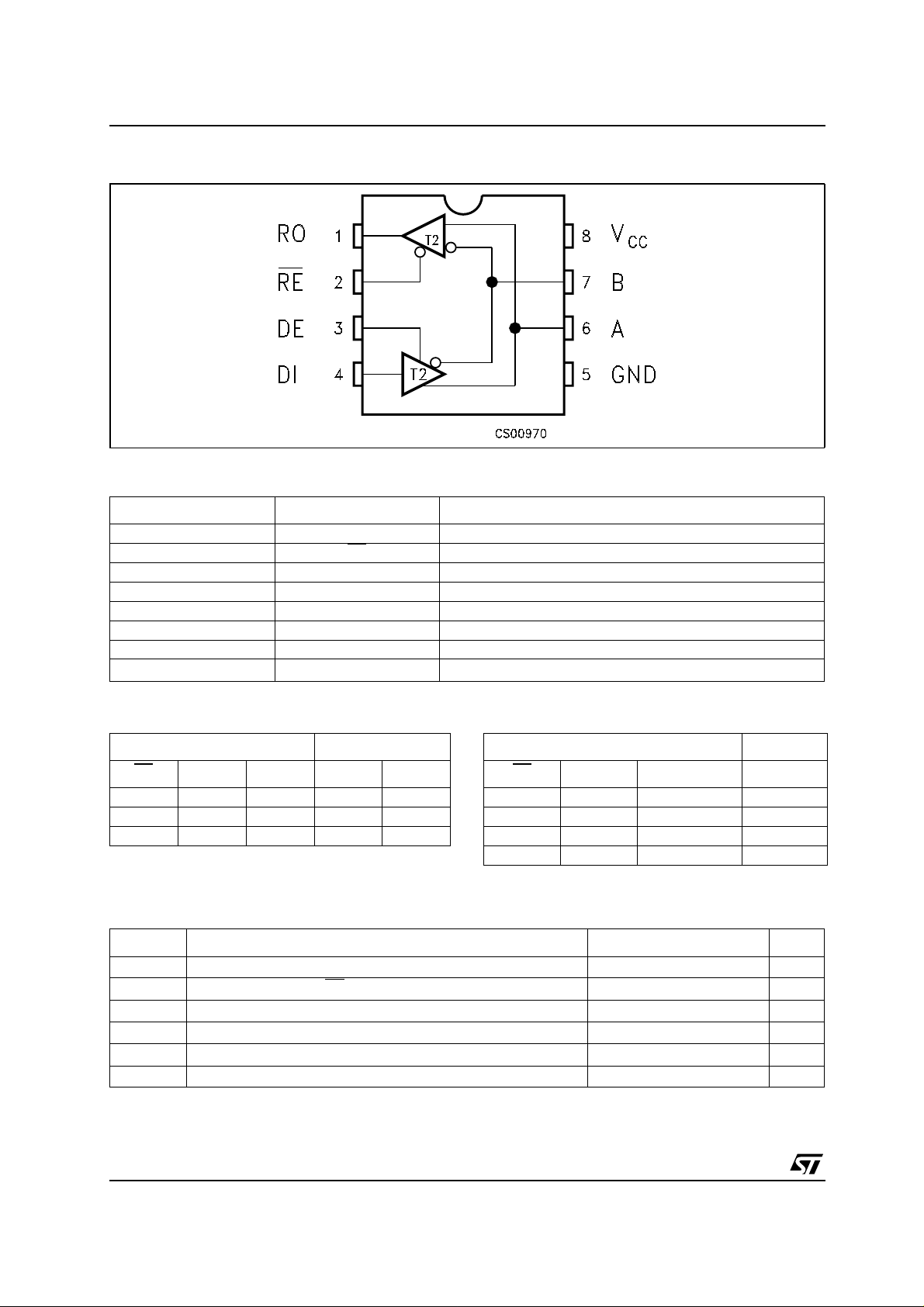
PIN CONFIGURATION
PIN DESCRIPTION
PlN N° SYMBOL NAME AND FUNCTION
1 RO Receiver Output
2RE
3 DE Driver Output Enable
4 DI Driver Input
5 GND Ground
6 A Non-inverting Receiver Input and Non-inverting Driver Output
7 B Inverting Receiver Input and Inverting Driver Output
8
Receiver Output Enable
V
CC
Supply Voltage
TRUTH TABLE (DRIVER)
INPUTS OUTPUTS
RE
XHHLH
XHLHL
XLXZZ
X= Don’t Care; Z=High Impedance
DE DI B A
TRUTH TABLE (RECEIVER)
INPUTS OUTPUT
RE
LL≥ +0.2V H
LL≤ -0.2V L
L L INPUTS OPEN H
HL X Z
X= Don’t Care; Z=High Impedance
DE A-B RO
ABSOLUTE MAXIMUM RATINGS
Symbol Parameter Value Unit
V
V
V
V
V
V
Absolute Maximum Ratings are those values beyond which damage to the device may occur. Functional operation under these condition is
not implied.
Supply Voltage
CC
Control Input Voltage (RE, DE) -0.5 to (VCC+ 0.5)
I
Driver Input Voltage (DI) -0.5 to (VCC+ 0.5)
DI
Driver Output Voltage (A, B)
DO
Receiver Input Voltage (A, B)
RI
Receiver Output Voltage (RO) -0.5 to (VCC+ 0.5)
RO
7V
V
V
± 14 V
± 14 V
V
2/13
ST75C176
DC ELECTRICAL CHARACTERISTICS
(V
=5V± 5%,TA=T
CC
(See Note 1)
Symbol Parameter Test Conditions Min. Typ. Max. Unit
V
V
∆V
V
∆V
V
∆V
V
V
I
I
OSD1
I
OSD2
I
Note 1: All currents into device pins are positive; all cuttents out of device pins are negative; all voltages are referenced to device ground
unless specified.
Note 2: Supply current specification is valid for loaded transmitters when V
Note 3: Applies to peak current. See typical Operating Characteristics.
Differential Driver Output
OD1
(No Load)
Differential Driver Output
OD2
(With Load)
Change in Magnitude of
OD
Driver Differential Output
Voltage for Complementary
Output States
Driver Common-Mode
OC
Output Voltage
Change in Magnitude of
OC
Driver Common-Mode
Output Voltage for
Complementary Output
States
V
Input High Voltage RE, DE, DI 2.0 V
IH
Input Low Voltage RE, DE, DI 0.8 V
V
IL
Input Current RE, DE, DI ± 2 µA
I
IN1
Input Current (A, B) VCM= 0V or 5.25V VDE=0V
I
IN2
Receiver Differential
TH
Threshold Voltage
Receiver Input Hysteresis VCM=0V 70 mV
TH
Receiver Output High
OH
Voltage
Receiver Output Low
OL
Voltage
3-State (High Impedance)
OZR
Output Current at Receiver
Receiver Input Resistance VCM= -7 to 12V 12 KΩ
R
IN
No Load Supply Current
I
CC
(Note 2)
Driver Short-Circuit Current,
=High
V
O
Driver Short-Circuit Current,
=Low
V
O
Receiver Short-Circuit
OSR
Current
MIN
to T
, unles s otherwise s pec ified. Typical v alues are referred to TA= 25°C)
MAX
5V
RL=27Ω (RS-485) (See Fig. 1)
R
=50Ω (RS-422) (See Fig. 1)
L
=27Ω or 50Ω (See Fig. 1) 0.2 V
R
L
1.5 5
5
RL=27Ω or 50Ω (See Fig. 1) 3 V
=27Ω or 50Ω (See Fig. 1) 0.2 V
R
L
V
V
IN
IN
= 12V
= -7V
1
-0.8
VCM= -7 to 12V -0.2 0.2 V
IO= -4mA VID= 200mV 3.5 V
IO=4mA VID= -200mV 0.4 V
VO= 0.4 to 2.4V ± 1 µA
VRE=0VorV
VDE=V
VDE=0V
V
= -7 to 12V (Note 3) 35 250 mA
O
V
= -7 to 12V (Note 3) 35 250 mA
O
VO=0VtoV
CC
CC
CC
DE
=0V
400
300
900
500
795mA
V
V
mA
mA
µA
µA
3/13
ST75C176
DRIVER SWITCHING CHARACTERISTICS
(V
=5V± 5%,TA=T
CC
(See Note 1)
Symbol Parameter Test Conditions Min. Typ. Max. Unit
t
t
t
t
t
t
t
Note 1: All currents into device pins are positive; all cuttents out of device pins are negative; all voltages are referenced to device ground
unless specified.
Propagation Delay Input to
PLH
Output
t
PHL
t
Output Skew to Output R
SK
Rise or Fall Time R
TLH
THL
Output Enable Time CL= 100pF S2 = Closed
PZH
Output Enable Time CL= 100pF S1 = Closed
PZL
Output Disable Time CL= 15pF S1 = Closed
PLZ
Output Disable Time CL= 15pF S2 = Closed
PHZ
MIN
toT
,unless otherwise specified. Typical values arereferred to TA=25°C)
MAX
R
=54Ω CL1=CL2= 100pF
DIFF
10 30 60 ns
(See Fig. 3 and 5)
=54Ω CL1=CL2= 100pF
DIFF
510ns
(See Fig. 3 and 5)
=54Ω CL1=CL2= 100pF
DIFF
31540ns
(See Fig. 3 and 5)
40 70 ns
(See Fig. 4 and 6)
40 70 ns
(See Fig. 4 and 6)
40 70 ns
(See Fig. 4 and 6)
40 70 ns
(See Fig. 4 and 6)
RECEIVER SWITCHING CHARACTERISTICS
(V
=5V± 5%,TA=T
CC
MIN
to T
, unles s otherwise s pec ified. Typical v alues are referred to TA= 25°C)
MAX
(See Note 1)
Symbol Parameter Test Conditions Min. Typ. Max. Unit
t
t
t
t
t
t
f
Note 1: All currents into device pins are positive; all cuttents out of device pins are negative; all voltages are referenced to device ground
unless specified.
Propagation Delay Input to
PLH
Output
t
PHL
Differential Receiver Skew R
SKD
Output Enable Time CRL= 15pF S1 = Closed
PZH
Output Enable Time CRL= 15pF S2 = Closed
PZL
Output Disable Time CRL= 15pF S1 = Closed
PLZ
Output Disable Time CRL= 15pF S2 = Closed
PHZ
Maximum Data Rate 2.5 Mbps
MAX
R
=54Ω CL1=CL2= 100pF
DIFF
(See Fig. 3 and 7)
=54Ω CL1=CL2= 100pF
DIFF
(See Fig. 3 and 7)
(See Fig. 2 and 8)
(See Fig. 2 and 8)
(See Fig. 2 and 8)
(See Fig. 2 and 8)
20 130 210 ns
13 ns
20 50 ns
20 50 ns
20 50 ns
20 50 ns
4/13
 Loading...