

.
HALFDUPLEX SYNCHRONOUS FSK MODEM
- TWO PROGRAMMABLE CHANNELS FOR
600BPS DATARATE
- TWO PROGRAMMABLE CHANNELS FOR
1200BPSDATARATE
.
AUTOMATICALL YTUNEDRxANDTxFILTER S
.
TX CARRIER FREQUENCIESSYNTHESIZED
FROMEXTERNALCRYSTAL
.
LOW DISTORTION Tx SIGNAL(S/H2≥ 50dB)
.
AUTOMATICLEVELCONTROLONTxSIGNAL
.
Rx SENSITIVITY: 2mV
3mV
.
Rx CLOCK RECOVERY
.
POWER-DOWN MODE
.
SUITABLETO APPLICATIONIN ACCORDANCE
WITH DH028/29 ENEL, EN50065- 1 CEN ELEC
ANDFCCSPECIFIC AT ION S
RMS
RMS
(600bps)
(1200bps)
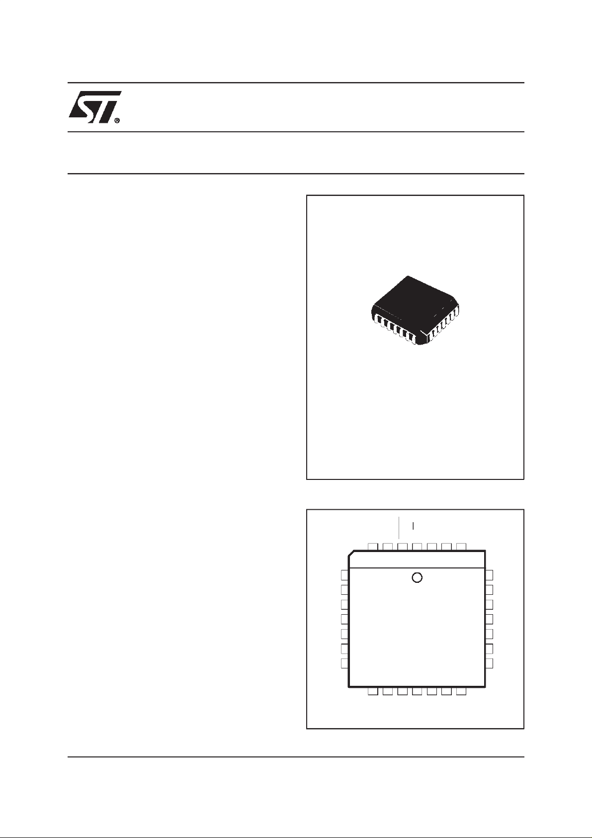
ST7536
POWER LINE MODEM
PLCC28
(Plastic Leaded Chip Carrier Package)
ORDER CODE : ST7536CFN
DESCRIPTION
The ST7536 is a half duplex synchronous FSK
MODEM designed for power line communication
networkapplications.
It operatesfrom a dual powersupply +5V and -5V,
and requires an external interface for the coupling
to the power line. It offerstwo programmable data
ratewith two programmablechannels each.
November 1998
PIN CONNECTIONS
TEST3
4
RxD
CLR/T
RxDEM
DGND
DV
TEST1
TEST2
5
6
7
8
9
DD
10
11
13
12
TxD
TEST4
3
XTAL2
RESET
2
15
14
CHS
XTAL1
Rx/Tx
1
ATO
28
16
BRS
ALCI
27
17
AFCF
TxFI
26
18
SS
DV
25
24
23
22
21
20
19
RxFO
RAI
V
A
DD
AGND
AV
SS
DEMI
IFO
7536-01.EPS
1/9

ST7536
PIN DESCRIPTION
Pin
Number
Name Type Description
1 Rx/Tx Digital Rx or Tx modeselection input
2 RESET Digital Logic reset and power-down mode input. Active when low.
3 TEST4 Digital Testinput whichselects the Tx band-pass filter input (TxFI)when high.
4 TEST3 Digital Testinputwhich gives an access to theclockrecovery inputstage. This input isselected
when TEST1 ishigh.
5 RxD Digital Synchronous receive data output
6 CLR/T Digital Rx or Tx clock according to the functional mode
7 RxDEM Digital Demodulated data output
8 DGND Supply Digital ground
9DV
Supply Digitalpositive supply voltage: 5V ± 5%
DD
10 TEST1 Digital Testinput which cancels the Tx to Rx mode automatic switching and validates TEST3
input. Active when high.
11 TEST2 Digital Testinputwhich reduces the Tx to Rxmode automaticswitching time. Active when high.
12 TxD Digital Transmitdata input
13 XTAL2 Digital Crystal oscillator output
14 XTAL1 Digital Crystal oscillator input
15 CHS Digital Channel selection input
16 BRS Digital Baud rate selection input
17 AFCF Analog Automatic frequency control output for connecting compensation network.
18 DV
Supply Digitalnegative supply voltage : -5V ± 5%
SS
19 IFO Analog Intermediate frequency filter output
20 DEMI Analog FSK demodulator input
21 AV
Supply Analog negative supply voltage : -5V±5%
SS
22 AGND Supply Analog ground : 0V
23 AV
Supply Analog positive supply voltage : 5V± 5%
DD
24 RAI Analog Receive analog input
25 RxFO Analog Receive filter output
26 TxFI Analog Transmitfilter input (selected when TEST4 ishigh)
27 ALCI Analog Automatic level control input
28 ATO Analog Analogtransmit output
7536-01.TBL
2/9
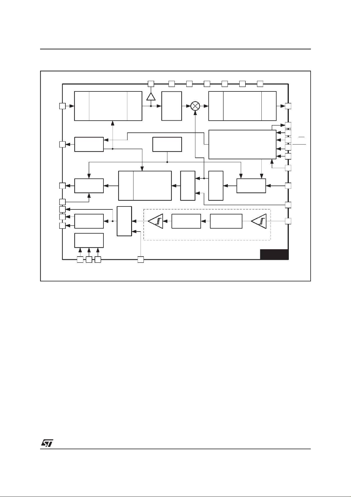
BLOCKDIAGRAM
ST7536
RAI
AFCF
ATO
ALCI
RxDEM
RxD
CLR/T
24
17
28
27
7
5
6
RX BAND-PASS
S.C. FILTER
A.A. FILTER
AFC
ALC
CLOCK
RECOVERY
TEST
LOGIC
SMT. FILTER
TX BAND-PASS
S.C. FILTER
A.A. FILTER
MUX
RxFO DGND AGND
25
DV
SS
18 23
20dB
GAIN
REFERENCE
VOLTAGE
POST-DEMO
S.C. FILTER
MUX
DV
DD
98
CORRELATOR
AV
SS
22
21
I.F. BAND-PASS
S.C. FILTER
A.A. FILTER
TIME BASE AND
CONTROLLOGIC
MODULATOR
A.A. FILTER
FSK DEMODULATOR
FSK
AV
DD
SMT. FILTER
19
13
14
1
2
16
15
12
26
20
IFO
XTAL2
XTAL1
Rx/Tx
RESET
BRS
CHS
TxD
TxFI
DEMI
10
11
TEST1
3
TEST2
TEST4
4
TEST3
ST7536
7536-02.EPS
3/9
 Loading...