

MULTIPLE RS-232 DRIVERS AND RECEIVERS
■ MEETS AND EXCEEDS THE
REQUIREMENTS OF EIA/TIA-232-E AND
ITUV.28 STANDARD
■ SINGLE CHIP WITH EASY INTERFACE
BETWEEN UART AND SERIAL PORT
CONNECTOR OF IBM PC/AT
COMPATIBLES
■ DESIGNED TO SUPPORT DATA RATESUP
TO 120 Kbps
DESCRIPTION
The ST75285 contains si x drivers and ten
receivers. The pinout matches the DB9S
connector design in order to decreas e the part
count, reduce the board space required and allow
easy interconnection of the UART and serial port
connector of IBM PC/AT
TM
bipolar circuits and processing of the ST75285
provides a rugged low-cost solution for this
function at the expense of quiescent power and
external passive component s relative to t he
ST75C185.
The S T75285 complies with the requirements of
the EIA/TIA 232-E and ITU (formally CCITT) v.28
standards. These standards are for data
interchange between a host comput er and
TM
AND
and compatibles. The
ST75285
TSSOP
peripheral at signalling rates up to 20k-bits/s. The
switching speeds of the ST75285 are fast enough
to support rates up to 120K-bits/s with lower
capacitive l oads (shorter cables). Interoperability
at the higher signalling rates cannot be assured
unless the designer has design control of the
cable and the inte rface circuits at the both ends.
For interoperability a t signalling rates to 120
K-bits/s, use of EIA/ITA-423-B (ITU v.10) and EIA/
ITA-422-B (ITU v.11) standards are
recommended. It allows space sav ing in
applications where two ST75185 are needed.
ORDERING CODES
Type
ST75285CTR 0 to 70 °C TSSOP38 (Tape & Reel) 2500 parts per reel
Temperature
Range
Package Comments
1/13December 2002
ST75285
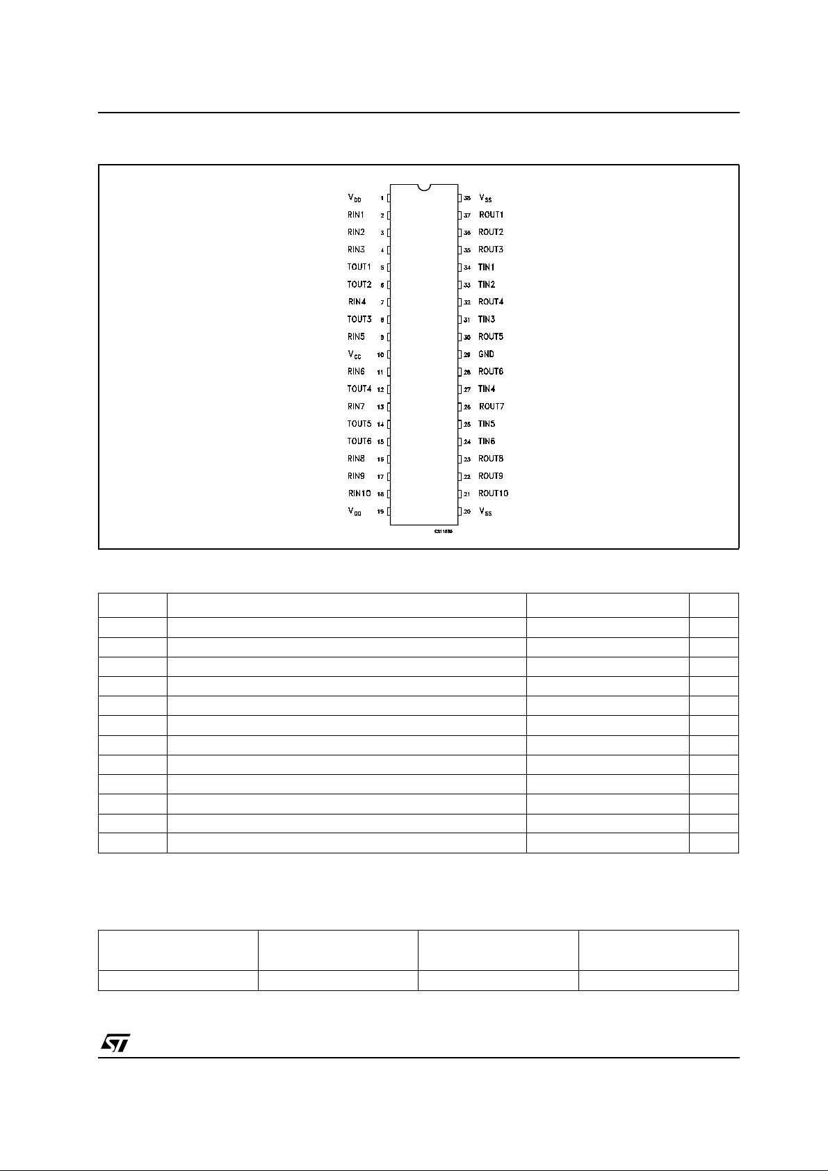
PIN DESCRIPTION
PlN N° SYMBOL NAME AND FUNCTION
1V
2 RIN1 First Receiver Input
3 RIN2 Second Receiver Input
4 RIN3 Third Receiver Input
5 TOUT1 First Driver Output
6 TOUT2 Second Driver Output
7 RIN4 Fourth Receiver Input
8 TOUT3 Third Driver Output
9 RIN5 Fifth Receiver Input
10
11 RIN6 Sixth Receiver Input
12 TOUT4 Fourth Driver Output
13 RIN7 Seventh Receiver Input
14 TOUT5 Fifth Driver Output
15 TOUT6 Sixth Driver Output
16 RIN8 Eighth Receiver Input
17 RIN9 Nineth Receiver Input
18 RIN10 Tenth Receiver Input
19
20 V
21 ROUT10 Tenth Receiver Ouput
22 ROUT9 Nineth Receiver Ouput
23 ROUT8 Eighth Receiver Ouput
24 TIN6 Sixth Driver Input
25 TIN5 Fifth Driver Input
26 ROUT7 Seventh Receiver Ouput
27 TIN4 Fourth Driver Input
28 ROUT6 Sixth Receiver Output
29 GND Ground
30 ROUT5 Fifth Receiver Output
31 TIN3 Third Driver Input
32 ROUT4 Fourth Receiver Output
33 TIN2 Second Driver Input
34 TIN1 First Driver Input
35 ROUT3 Third Receiver Ouput
36 ROUT2 Second Receiver Ouput
37 ROUT1 First Receiver Ouput
38 V
DD
V
CC
V
DD
SS
SS
Supply Voltage (+12V)
Supply Voltage (-12V)
Supply Voltage (-12V)
Supply Voltage (+5V)
Supply Voltage (+5V)
2/13
PIN CO NNECTION IEC LOGIC SYMBOL AND LOGIC DIAGRAM
ST75285
ABSOLUTE MAXIMUM RATINGS OVER OPERATING FREE-AIR TEMPERATURE RANGE
Symbol Parameter Value Unit
V
V
V
V
V
V
I
P
T
T
ESD Human Body Model
T
Absolute Maximum Ratings are those values beyond which damage to the device may occur. Functional operation under these condition is
not implied.
NOTE 1: All voltage are with respect to the network ground terminal.
Supply Voltage (Note 1)
DD
Supply Voltage (Note 1)
SS
Supply Voltage (Note 1)
CC
Input Voltage Range (DRIVER)
I
Input Voltage Range (RECEIVER)
I
Output Voltage Range (DRIVER)
O
Receiver Low Level Output Current
O
Continuous Total Power Dissipation
D
Operating Free-Air Tempereature Range
A
Storage Temperature Range
stg
Lead Temperature 1.6mm from case for 10 sec
L
-0.3 to 15 V
0.3 to -15 V
-0.3 to 10 V
-15 to 7 V
-30 to 30 V
-15 to 15 V
20 mA
See dissipation Rating Table
0to70 °C
-65 to + 150 °C
>2 kV
260 °C
DISSIPATION RATING TABLE
Package
TSSOP (T)
(*) This is the reverse of the traditional junction-case thermal resistance R
Power Rating
at T
≤ 25°C
A
1277 mW 10.2 mW/°C 644 mW
Derating Factor
above TA= 25°C (*)
tJ-C
Power Rating
at TA≤ 85°C
3/13
ST75285
RECOMMENDED OPERATING CONDITIONS
Symbol Parameter Min Max Unit
V
V
V
V
I
OH
I
T
SUPPLY CURRENTS
Supply Voltage
DD
Supply Voltage
SS
Supply Voltage
CC
Driver Input Voltage
I
High Level Output Current DRIVER -6
RECEIVER -0.5
Low Level Output Current DRIVER 6
OL
Operating Free-Air Tempereature
A
RECEIVER 16
7.5 15 V
-7.5 -15 V
4.5 5.5 V
0
V
CC
070°C
V
mA
mA
Symbol Parameter
I
I
I
Supply Current from V
DD
Supply Current from V
SS
Supply Current from V
CC
DD
SS
CC
V
DD
V
SS
Min. Typ. Max.
9 -9 No load.
12 -12 28
15 -15 32
All inputs at
1.9V
9 -9 No load.
12 -12 11
15 -15 12
All inputs at
0.8V
9 -9 No load.
12 -12 -28
15 -15 -32
9 -9 No load.
12 -12 -6.4
15 -15 -6.4
All inputs at
1.9V
-6.4 mA
All inputs at
0.8V
No load. All inputs at 5V
=5V
V
CC
22 mA
9mA
-22 mA
60 mA
Unit
DRIVER EL ECTRICAL CHARACTERISTICS OVER OPERATING FREE-AIR TEMPERATURE
Test Conditions Value
RANGE (V
Symbol Parameter Test Conditions
V
OH
V
OL
I
IH
I
IL
I
OS(H)
I
OS(L)
R
O
NOTE 3: The algebraic convention, where the more positive (less negative) limits designated as maximum, is used in this datasheetforlogic
levels only (e.g. if - 10V is a maximum, the typical value is a more negative voltage).
NOTE 4: Output short circuit conditions must maintain the total power dissipation below absolute maximum ratings.
NOTE 5: Test conditions are those specified by EIA-232-E and as listed above.
=9V,VSS=-9V,VCC= 5V, unless oth erwise specified)
DD
Value
Unit
Min. Typ. Max.
High Level Output Voltage VIL=0.8V RL=3KΩ(See Figure 1) 6 7.5 V
Low Level Output Voltage
VIH=1.9V RL=3KΩ(See Figure 1) -7.5 -6 V
(Note 3)
High Level Input Current VI= 5 V (See Figure 2) 10 µA
Low Level Input Current VI= 0 V (See Figure 2) −1.6 mA
High Level Short Circuit
VIL=0.8V VO= 0 V (See Figure 1) -4.5 −12 −19.5 mA
Output Current (Note 4)
Low Level Short Circuit
VIH=2V VO= 0 V (See Figure 1) 4.5 12 19.5 mA
Output Current
Output Resistance VDD=VSS=VCC=0V
V
= -2 to 2 V (Note 5)
O
300 Ω
4/13

DRIVER SWITC HING CHARACTERISTICS (VDD= 12V, VSS= -12V, VCC=5V,TA=25°C)
ST75285
Symbol Parameter Test Conditions
Value
Min. Typ. Max.
t
t
t
Propagation Delay Time, Low to High
PLH
Level Output
Propagation Delay Time, High to Low
PHL
Level Output
Transition Time Low to High Level
TLH
Output
RL=3to7KΩ CL=15pF
(See Figure 3, 4)
RL=3to7KΩ CL=15pF
(See Figure 3, 4)
RL=3to7KΩ CL=15pF
(See Figure 3, 4)
=3to7KΩ CL= 2500 pF
R
L
200 400 ns
50 100 ns
60 100 ns
1.7 2.5 µs
(Note 6, See Figure 3, 4)
t
Transition Time High to Low Level
THL
Output
RL=3to7KΩ CL=15pF
(See Figure 3, 4)
=3to7KΩ CL= 2500 pF
R
L
50 100 ns
1.5 2.5 µs
(Note 6, See Figure 3, 4)
NOTE 6: Measured between -3V and 3V points of output waveform (EIA-232-E conditions), all unused inputs are tied.
RECEIVER ELECTRICAL CHARACTERISTICS OVER OPERATING CONDITIONS
Symbol Parameter Test Conditions
Positive Going Threshold Voltage (See Figure 6) 2.2 2.4 V
V
T+
Negative Going Threshold Voltage TA= 25 °C (See Figure 6) 0.75 0.97 V
V
T-
V
V
Input Hysteresis (VT+-VT-) 0.5 V
hys
High Level Output Voltage IOH= -0.5mA VIH= 0.75 V 2.6 4 5 V
OH
Inputs Open 2.6
V
Low Level Output Voltage VI=3V IOL= 10 mA 0.2 0.45 V
OL
High Level Input Current VI= 25 V (See Figure 6) 3.6 8.3 mA
I
IH
= 3 V (See Figure 6) 0.43
V
I
Low Level Input Current VI= -25 V (See Figure 6) -3.6 -8.3 mA
I
IL
= -3 V (See Figure 6) -0.43
V
I
Short-Circuit Output Current VI=0V VO=0V
I
OS
(See Figure 5)
All typical values are at TA = 25°C, VCC = 5V, VDD = 9V and VSS=-9V
Min. Typ. Max.
Value
-3.4 -12 mA
Unit
Unit
RECEIVER SWITCHING CHARACTERISTICS (VDD=12V,VSS=-12V,VCC=5V TA= 25°C)
Symbol Parameter Test Conditions
t
PLH
t
PHL
t
TLH
t
THL
Propagation Delay Time Low to High
Level Output
Propagation Delay Time High to Low
Level Output
Transition Time Low to High Level
Output
Transition Time High to Low Level
Output
RL=5KΩ CL=50pF
(See Figure 6)
RL=5KΩ CL=50pF
(See Figure 6)
RL=5KΩ CL=50pF
(See Figure 6)
RL=5KΩ CL=50pF
(See Figure 6)
Min. Typ. Max.
Value
200 500 ns
60 120 ns
200 525 ns
20 60 ns
Unit
5/13

ST75285
Figure 1 : Driver Test Circuit for VOH,I
SO(H)
Figure 2 : Driver Test Circuit for IIHand I
and I
SO(L)
IL
Figure 3 : Driver Test Circuit
6/13

Figure4 : Driver Voltage Wavef orm s
ST75285
Figure5 : Receiver T es t Circuit for I
OS
Figure6 :Receiver Test Circuit for VT,VOH,V
OL
7/13

ST75285
Figure7 : Receiver Test Circuit
Figure8 : Receiver Voltage Waveforms
NOTE A: The pulse generator has the following characteristics: tW= 25µs, PRR = 20KHz, ZO=50Ω,tr=tf< 50ns
NOTE B: C
includes probe and jig capacitance.
L
8/13

ST75285
Figure9 : Driver Voltage Transfer Characteristics
Figure10 : Driver Short Circuit Output Current vs
Free-Air Temperature
Figure12 : Driver Output Current v s Output
Voltage
Figure13 : Driver Output Slew Rate vs Load
Capacitance
Figure11 : Rec eiver Threshold vs S upply
Voltage
Figure14 : Receiver Threshold vs Temperature
9/13

ST75285
APPLICATION INFORM ATION: DIODES ON POWER SUPPLY
Diodes placed in series with the VDD and VS S leads protect the ST75 185 in the fault condition in which
the devices output are shorted to ±15V and th e power supplies are at low state and provide
low-impedance path to ground (see Figure below).
10/13

ST75285
TSSOP38 MECHANICAL DATA
mm. inch
DIM.
MIN. TYP MAX. MIN. TYP. MAX.
A 1.2 0.047
A1 0.05 0.15 0.002 0.006
A2 0.8 1 1.05 0.031 0.039 0.041
b 0.17 0.27 0.0067 0.011
c 0.09 0.20 0.0035 0.0079
D 9.6 9.7 9.8 0.378 0.381 0.385
E 6.2 6.4 6.6 0.244 0.252 0.260
E1 4.3 4.4 4.5 0.169 0.173 0.177
e 0.5 0.0197
K0˚ 8˚0˚ 8˚
L 0.50 0.6 0.75 0.020 0.023 0.030
A2
A
A1
b
e
D
K
c
E1
L
E
PIN 1 IDENTIFICATION
1
0117861/B
11/13

ST75285
Tape & Reel TSSOP38 MECHANICAL DATA
mm. inch
DIM.
MIN. TYP MAX. MIN. TYP. MAX.
A 330 12.992
C 12.8 13.2 0.504 0.519
D 20.2 0.795
N 60 2.362
T 22.4 0.882
Ao 6.8 7 0.268 0.276
Bo 10.1 10.3 0.398 0.406
Ko 1.7 1.9 0.067 0.075
Po 3.9 4.1 0.153 0.161
P 11.9 12.1 0.468 0.476
12/13

ST75285
Information furnished is believed to be accurate and reliable. However, STMicroelectronics assumes no responsibi lity f or the
consequences of use of such informatio n nor for any infringement of paten ts or o ther rig hts of t hird part ies which ma y result from
its use. No license is granted by implication or otherwise under any patent or patent rights of STMicroelectronics. Specifications
mentioned in this publication are subject to change without notice. This publication supersedes and replaces all information
previousl y suppl ied. STM icroel ectronics produc ts are not auth orized for use as c ritica l compone nts in l ife s upport dev ices or
systems without express written approval of STMicroelectronics.
Australia - Brazil - Canada - China - Finland - France - Germany - Hong Kong - India - Israel - Italy - Japan - Malaysia - Malta - Morocco
© The ST logo is a registered trademark of STMicroelectronics
© 2002 STMicroelectronics - Printed in Italy - All Rights Reserved
STMicroelectronics GROUP OF COMPANIES
Singapore - Spain - Sweden - Switzerland - United Kingdom - United States.
© http://www.st.com
13/13
 Loading...