

SGS Thomson Microelectronics ST63T73J5B1, ST6373, ST63E73J5D1, ST6373J5B1, ST6373J3B1 Datasheet
...
R
ST6373
8-BIT ROM/OTP/EPROM MCUs FOR DIGITALLY
CONTROLLED MULTISYNC/MULTISTANDARD MONITORS
■ 4.5V to 6V Operating Supply Voltage Range
■ Low Current Consumption
■
0to+70°C Operating Temperature Range
■
8 MHzclock Oscillator
■ 16K bytes ROM/OTP/EPROM
(8K and 12K ROM versions also available)
■
192 bytes RAM
■ 384 bytes general purpose EEPROM
■ 128 bytes dedicated EEPROM for DDC SPI
■ 22 fully programmable I/O pins, offering direct
LED drive capability, as well as interrupt
generation for keyboard inputs
■ Digital WATCHDOG timer
■ Three Timers, each comprising an 8-bit counter
and a 7- bit Prescaler
■ SYNC Processor:
– 12-bits HSYNC Event Counter
– 12-bits VSYNC Period Counter
– HSYNC and VSYNC Polarity Detection
– HSYNC and VSYNC Outputs
– HFLYBACK and VFLYBACK Inputs
– CLAMP and BLANK Outputs
■ 14-bit (PWM + BRM) D/A Converter
■ Nine 7-bit PWM D/A Converter Outputs
■
8-bit A/D Converter with 8 multiplexed inputs
■ DDC SPI with interrupt and 4 operating modes
■ A further SPI with interrupt and 2 operating
modes
■
Remote Control Signal Input (Non Maskable
Interrupt)
■ VSYNC Interrupt Input
■ Five Interrupt Vectors
■
XOR Register (Instruction Set expansion)
■ MIRROR Register (Instruction Set expansion)
(Refer to end of Document for Ordering Information)
PSDIP42
CSDIP42
February 1998 1/64
ThisisadvanceinformationfromSGS-THOMSON.Detailsaresubject tochangewithoutnotice.
1

Table of Contents
ST6373 . . . . . . . . . . . . . . . . . . . . . . . . . . . . . . . . . . . . . . . . . . . . .1
1 GENERAL DESCRIPTION . . ....................................................4
1.1 INTRODUCTION . . . . . . . ..................................................4
1.2 PIN DESCRIPTION . . . . . . . ................................................6
1.3 MEMORY SPACES .......................................................8
1.3.1 Stack Space . . . . . . . . . . ..............................................8
1.3.2 Program Space . .. . . ................................................8
1.3.3 Data Space .......................................................10
1.3.4 Data RAM/EEPROM ................................................12
1.3.5 EEPROM Description . . . . . . . . . . . . . ..................................12
1.4 MEMORYPROGRAMMING ...............................................15
1.4.1 Program Memory . . . . . . . . . ..........................................15
1.4.2 Option Byte .......................................................15
1.4.3 Eprom Erasure . . . . . . . ..............................................15
2 CENTRAL PROCESSING UNIT . . . ..............................................16
2.1 INTRODUCTION . . . . . . . .................................................16
2.2 CPU REGISTERS .......................................................16
3 CLOCKS, RESET, INTERRUPTS AND POWER SAVING MODES .....................18
3.1 ON-CHIP CLOCK OSCILLATOR. . . . . . . . . . . . . . . . . . . . . . . . . . . . ................18
3.2 RESETS...............................................................19
3.2.1 RESET Input . . . . . . . ...............................................19
3.2.2 Power-on Reset . . . . . . . . . . . . . . . .....................................19
3.2.3 Watchdog Reset . ..................................................20
3.2.4 Application Note . . . . . . . . . . . . . . . .....................................20
3.2.5 MCU Initialization Sequence ..........................................20
3.3 HARDWARE ACTIVATED DIGITAL WATCHDOG FUNCTION . .. . . ...............21
3.4 INTERRUPT . . . . . . . . . . .. . . . .. . . .........................................23
3.4.1 Interrupt Vectors/Sources . ...........................................23
3.4.2 Interrupt Priority . . . . . . . . . . . . . . . .....................................24
3.4.3 Interrupt Option Register . . . . . . . . . . . . . . . . . . . . . ........................24
3.4.4 Interrupt Procedure .................................................25
3.4.5 ST6373 Interrupt Details . . . . . . . . . . . . . . . . . . . . . ........................25
3.5 POWER SAVING MODES. . . ..............................................28
3.5.1 WAIT Mode .......................................................28
3.5.2 STOP Mode . . . . . . . . . . . ............................................28
3.5.3 Exit from WAIT Mode . . . . . . . .........................................28
4 ON-CHIP PERIPHERALS ......................................................29
4.1 I/OPORTS.............................................................29
4.1.1 Details of I/O Ports A and B . . . . . . . . . . . . . . . . . . .........................30
4.1.2 Details of I/O Port C . . . ..............................................31
4.1.3 I/O Port Registers ..................................................34
4.2 TIMERS ...............................................................35
4.2.1 Timer Operating Modes . . . . ..........................................36
4.2.2 Timer StatusControl Registers (TSCR). . . ...............................37
4.2.3 Timer Counter Registers (TCR) . . . . . . . . . . . . . . .. . . . .....................37
64
2/64

Table of Contents
4.2.4 Timer Prescaler Registers (PSC). . .....................................37
4.3 A/D CONVERTER (ADC) . . . . . . . . ..........................................38
4.3.1 Application Notes . . . . . . . . . ..........................................38
4.4 SYNC PROCESSOR . . . . . . . ..............................................40
4.4.1 Event Counter . . ...................................................40
4.4.2 Period Counter . . . . . . . ..............................................40
4.4.3 Polarity Detector . ..................................................40
4.4.4 Output Polarity Control ...............................................40
4.4.5 Video Blanking Generator . ...........................................41
4.5 14-BIT PWM D/A CONVERTER ............................................44
4.5.1 Output Details . . ...................................................44
4.5.2 HDA Tuning Cell Registers ...........................................44
4.6 7-BIT PWM D/A CONVERTERS ............................................45
4.6.1 Digital Outputs . . . . . . . ..............................................45
4.7 SERIAL PERIPHERAL INTERFACES. . . . . . . . . . . . . . . . . . . .....................46
4.7.1 SPI Modes ........................................................47
4.8 MIRROR REGISTER . . . . . . . ..............................................51
4.9 XOR REGISTER . . . . . . . .................................................51
5 SOFTWARE . . . . . . . . . .......................................................52
5.1 ST6 ARCHITECTURE . . . . . . . . . . . . . . . .....................................52
5.2 ADDRESSING MODES . . . . . . . . ...........................................52
5.3 INSTRUCTION SET ......................................................53
6 ELECTRICAL CHARACTERISTICS. . . . ..........................................58
6.1 ABSOLUTE MAXIMUM RATINGS. . . . . . . . . . . . . . . . . . .........................58
6.2 RECOMMENDED OPERATING CONDITIONS. . . . .............................58
6.3 DC ELECTRICAL CHARACTERISTICS . . ....................................59
6.4 AC ELECTRICAL CHARACTERISTICS . .....................................60
7 GENERAL INFORMATION . . . . . . . ..............................................61
7.1 PACKAGE MECHANICAL DATA. . . . . . . . .. . . . . . . . . . . . . . . . . . . ................61
7.2 ORDERING INFORMATION . . . . . . . . .. . . . ..................................62
3/64
1

ST6373
1 GENERAL DESCRIPTION
1.1 INTRODUCTION
ST6373 Microcontrollers are members of the 8-bit
HCMOS ST637x family, a series of devices specially intended for Digitally Controlled Multi Frequency Monitor applications. All ST637x devices
are based on a building block approach: a common core is surrounded by a combination of onchip peripherals (macrocells) available from a
standard library.
ST6373 devices are available in functionally identical ROM, OTP (ST63T73) and EPROM
(ST63E73) versions, all with the same pinout.
ROM devices are available with 8, 12 or 16K Program memory, whereas OTP and EPROM versions are both available in 16K versions only. For
details relating to sales types, refer to Section 7.2.
Since ROM, OTP and EPROM versions are
functionally identical, the present Datasheet
will refer to the generic ST6373 device, except
where specific versions differ in detail.
The ST6373 devices feature:
– Nine PWM outputs, which can be used as Digital
to Analog converter outputs (withexternal RC filters). These are suitable for tuning and other
functions.
– A PWM output with Bit Rate Multiplier, to which
the above comments apply.
– An Event Counter especially designed to calcu-
late the HSYNC (or HDRIV) Frequency, using
one of the on-chip timers.
– A Period Counter especially designed to calcu-
late the VSYNC Period.
– A Polarity Detector for HSYNC (or HDRIV) and
VSYNC.
– HSYNC and VSYNC outputs with controlled po-
larity.
– Video Blanking and Clamping Outputs.
– Two I/O ports A & B usable for a keyboard wake-
up feature since an interrupt input ored on each
of their pins.
– An Analog to Digital converter connected to port
B which can be used to decode an analog key-
board or for AFC.
– A VSYNC input pin connected to an interrupt
vector and to the DDC SPI for DDC1 protocol.
– An NMI inputwhich canbe used, forexample, as
a Remote Control input for a TV application.
– A hardware DDC SPI able to manage DDC1
(VSYNC as clock), DDC2B and DDC2AB (I2C
BUS Multimaster and Slave). A 128-byte
dedicated EEPROM memory is available for
DDC1 and DDC2B.
– Hardware I2C SPI for internal monitor bus and to
manage, for example, an OSD.
– A Mirror Register and a XOR Register are includ-
ed to complement the basic ST6 instruction set.
Table 1. ST6373 Device Summary
DEVICE
CONFIGURATION
ST6373
ST63T73 16K OTP 192 512 8 1 9 ST63E73 16K EPROM 192 512 8 1 9 -
Note: See
4/64
Ordering Information in Table 23 at the end of the Datasheet.
Program
Memory
(Bytes)
8K ROM
12K ROM
16K ROM
RAM
(Bytes)
192 512 8 1 9 ST63E73,ST63T73
EEPROM
(Bytes)
A/D
Inputs
14-bit
D/ (PWM)
Output
7-bit
D/A (PWM)
Output
EMULATING
DEVICES
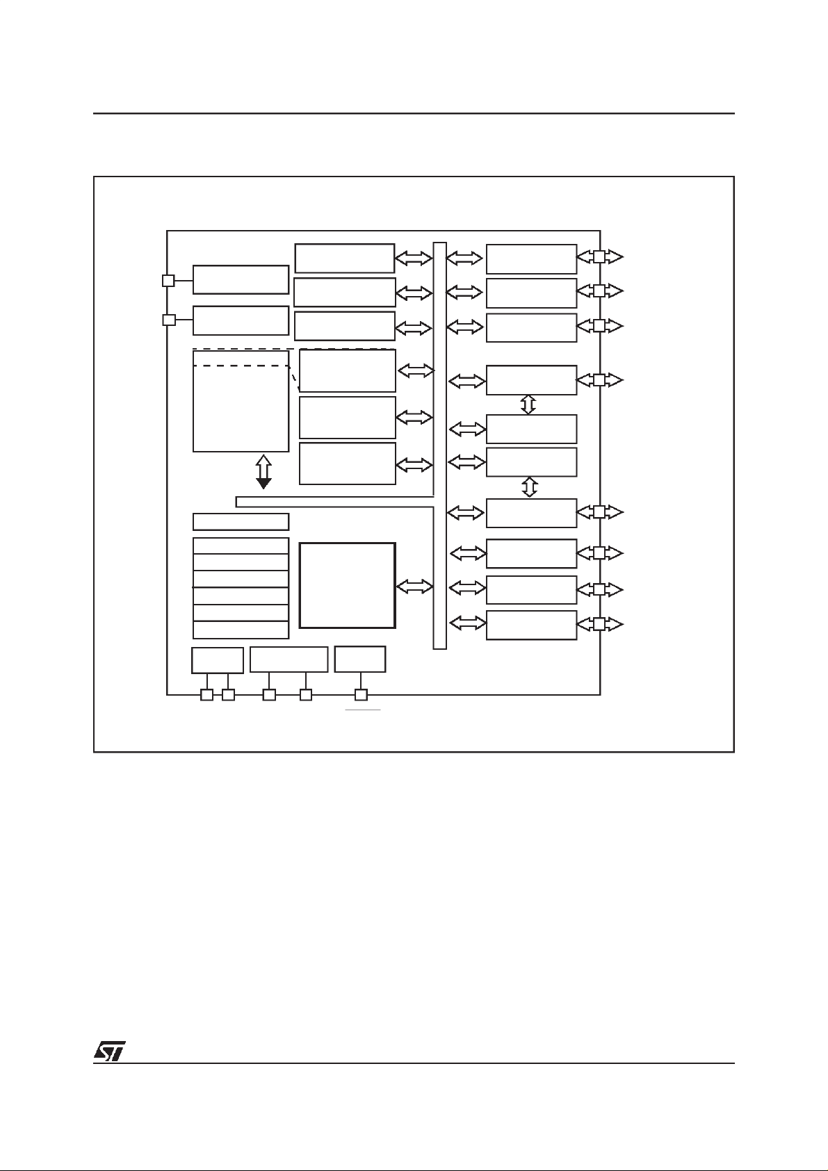
Figure 1. ST6373 Block Diagram
ST6373
TEST/V
(**)
PP
NMI
VSYNC
PWRIN
TEST
INTERRUPT
Inputs
USER PROGRAM
MEMORY
16 KBytes
PC
STACK LEVEL1
STACK LEVEL2
STACK LEVEL3
STACK LEVEL4
STACK LEVEL5
STACK LEVEL6
POWER
SUPPLY
OSCILLATOR
TIMER 1
TIMER 2
DIGITAL
WATCHDOG/TIMER
DATA ROM
USER
SELECTABLE
DATARAM
192 Bytes
DATA EEPROM
384 Bytes
8 BIT CORE
RESET
PORT A
PORT B
PORT C
DDC SPI (1)
EEPROM
128 Bytes (1)
TIMER 3
SYNC
PROCESSOR
I C SPI
D/A Outputs
A/D Inputs
PA0 -> PA7*
PB0 -> PB7*
PC0 -> PC7*
SCLD, SDAD
VSY NC, EXTCLK
HSYNC O, VSYNCO
HSYNC I, VSYNCI
HDRIV
HFLY, VFL Y
CLMPO, BLK O
SCLI, SDAI
HDA, DA0 -> DA8
AD0 -> AD7
V
DDVSS
OSCin OSCout RESET
(*)Refer to Pin Description for Add itional Information
(**)VPPinput for OTP/EPROM deviceprogramming
5/64
ST6373
1.2 PIN DESCRIPTION
VDDand V
these two pins. VDDis power and VSSis the
Power is supplied to the MCU using
SS.
ground connection.
OSCin, OSCout.
These pins are internally connected to the on-chip oscillator circuit. A quartz
crystal or a ceramic resonator can be connected
between these two pins in order to allow the correct operation of the MCU with various stability/cost trade-offs. The OSCin pin is the input pin,
the OSCout pin is the output pin.
RESET. The active lowRESETpin is used to start
the microcontroller to the beginning of its program.
Additionally the quartz crystal oscillator will be disabled when theRESET pin is low toreduce power
consumption during reset phase.
TEST
. The TEST pin mustbe held at VSS for nor-
mal operation.
PA0, PA1, PA2/HSYNCO, PA3/VSYNCO,
PA4/CLMPO, PA5/BLKO, PA6/SCLI, PA7/SDAI
Port A.
–
Software configurable as push-pull output, open-drain output, Schmitt trigger input with
or without pull-up. Port A inputs can be also
ORed into the INT1 interrupt. Port A outputs
have a LED drive capability (10 mA). Pins PA2
and PA3 can be configured respectively as
HSYNC and VSYNC outputs.Pins PA4 and PA5
can be configured respectively as CLAMP and
BLANK Outputs.Pins PA6 and PA7 can be configurated as the I2C SPI pins SCLI and SDAI.The
push-pull output and the input pull-up options do
not exist for these two pins. After reset the PA0
to PA5 pins are configured as inputs with pull-up.
PB0/AD0, PB1/AD1, PB2/AD2, PB3/AD3,
PB4/AD4, PB5/AD5/HFLY, PB6/AD6/VFLY,
PB7/AD7
Port B
–
. Each pin can be software configured as
push-pull output, open-drain output, Schmitt trigger inputwith or without pull-up.Port B inputs can
be also ored into the INT1 interrupt. Pins PB5
and PB6 can be configured as HFLY and VFLY
inputs. In addition, any pin of port B can be software selected as the Analog-to-Digital converter
input. Only one pin should be selected at a time,
otherwise a conflict would result. After reset the
port B pins are configured as inputs with pull-up.
PC0/SCLD, PC1/SDAD, PC2, PC3/EXTCLK,
PC4/PWRIN, PC5, PC6/HSYNC, PC7/HDRIV
– Port C. Software configurable as open-drain out-
puts or Schmitt trigger inputs with or without pullups. When configured as outputs, pins PC0 to
PC3 are configured as 5V open-drain. Pins PC4
to PC7 are configured as open-drain 12V; the input pull-up option does not exist for these four
pins. Pins PC0, PC1 and PC3 can be configured
as the DDCSPI pins SCLD, SDADand EXTCLK.
The input pull-up option does not exist for PC0
and PC1. Pins PC6 and PC7 can be configured
as HSYNC and HDRIV inputs.After reset: PC3 is
configured as input with pull-up. PC0, PC1 &
PC4 to PC7 are configured in input without pullup. PC2 is in output mode with the value 1 (high
impedance).
DA0-DA8. These pins are the nine PWM D/A outputs of the on-chip D/A converters. These lines
have push-pull outputs with 5V drive. The output
repetition rate is 31.25KHz (with 8MHz clock).
VSYNC. This is the Vertical Synchronization pin.
This pin is connected to an internal interrupt and is
configured as input with pull-up and Schmitt trigger.
HDA. This is the output pin of the on-chip 14-bit
PWM D/A Converter. This line is a push-pull output with standard drive.
NMI
. This pin is the Non-Maskable interrupt input
and is configured as input withpull-up and Schmitt
trigger.
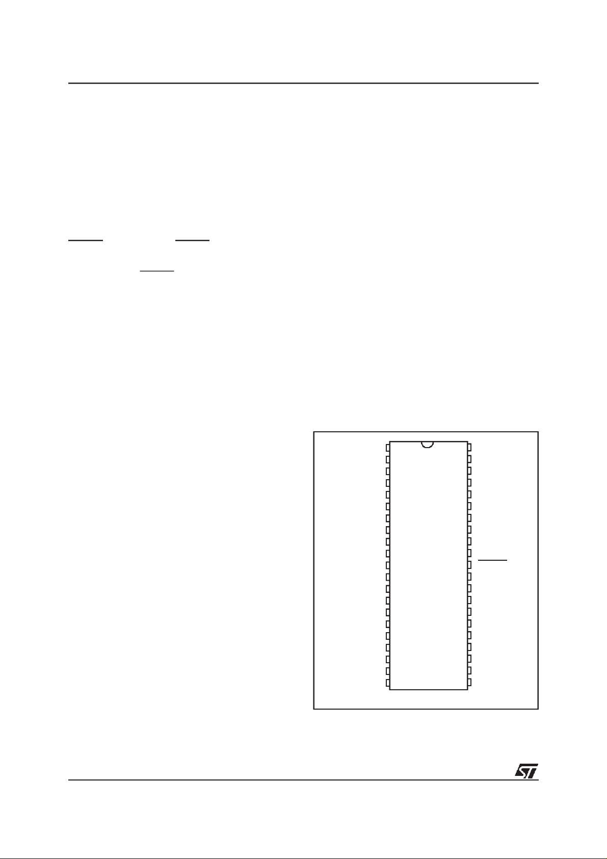
Figure 2. ST6373 Pin configuration
V
DD
O0/DA0
O1/DA1
O2/DA2
O3/DA3
AD0/PB0
AD1/PB1
AD2/PB2
AD3/PB3
AD4/PB4
HFLY/AD5/PB5
VFLY/AD6/PB6
AD7/PB7
PA0
PA1
HSYNCO/PA2
VSYNCO/PA3
CLMPO/PA4
BLKO/PA5
SCLI/PA6
SDAI/PA7
(1) This pin is also the VPPinput for OTP/EPROM devices
1
2
3
4
5
6
7
8
9
10
11
12
13
14
15
16
17
18
19
20
V
SS
21
42
PC0/SCLD
41
PC1/SDAD
40
PC2
39
PC3/EXTCLK
38
PC4/PWRIN
37
PC5
36
PC6/HSYNC
35
PC7/HDRIV
34
HDA
33
RESET
32
OSCout
31
OSCin
30
TEST/V
29
28
VSYNC
27
NMI
26
DA4/O4
25
DAR/O5
24
DA6/O6
23
DA7/O7
22
DA8/O8
PP
(1)
6/64

Table 2. Pin Summary
Pin Function Description
DA0 to DA8 Output, Push-Pull
HDA Output, Push-Pull
NMI Input, Pull-up, Schmitt Trigger Input
VSYNC Input, Pull-up, Schmitt Trigger
TEST Input, Pull-Down
OSCin Input, Resistive Bias, SchmittTrigger to Reset Logic Only
OSCout Output, Push-Pull
RESET Input, Pull-up, Schmitt Trigger Input
PA0-PA5 I/O, Push-Pull/Open Drain, Software Input Pull-up, Schmitt Trigger Input
PA6-PA7 I/O, Open-Drain, No Input Pull-up, Schmitt Trigger Input
PB0-PB7 I/O, Push-Pull/Open Drain, Software Input Pull-up, Schmitt Trigger Input, Analog Input
PC0-PC1 I/O, Open-Drain, No Input Pull-up, Schmitt Trigger Input
PC2-PC3 I/O, Open-Drain, 5V, Software Input Pull-up, Schmitt Trigger Input
PC4-PC7 I/O, Open-Drain, 12V, No Input Pull-up, Schmitt Trigger Input
V
DD,VSS
Power Supply Pins
ST6373
7/64
ST6373
1.3 MEMORY SPACES
The MCU operates in three different memory
spaces: Stack Space, Program Space and Data
Space.
1.3.1 Stack Space
The stackspace consists of six 12bit registers that
are used for stacking subroutine and interrupt return addresses plus the current program counter
register.
1.3.2 Program Space
The program space is physically implemented in
the ROM and includes all the instructions that are
to be executed, as well as the data required for the
immediate addressing mode instructions, the reserved test area and user vectors. It is addressed
thanks to the 12-bit Program Counter register (PC
register) and theST6 Corecan directly address up
to 4K bytes of Program Space. Nevertheless, the
Program Space can be extended by the addition
of 2-Kbyte memory banks as it is shown inFigure
2, in which the 16K bytes memory is described.
These banks are addressed by pointing to the
000h-7FFh locations of the Program Space thanks
to the Program Counter, and by writing the appropriate code in the Program ROM Page Register
(PRPR) located at address CAh in the Data
Space. Because interrupts and common subrouroutines should be available all the time only the
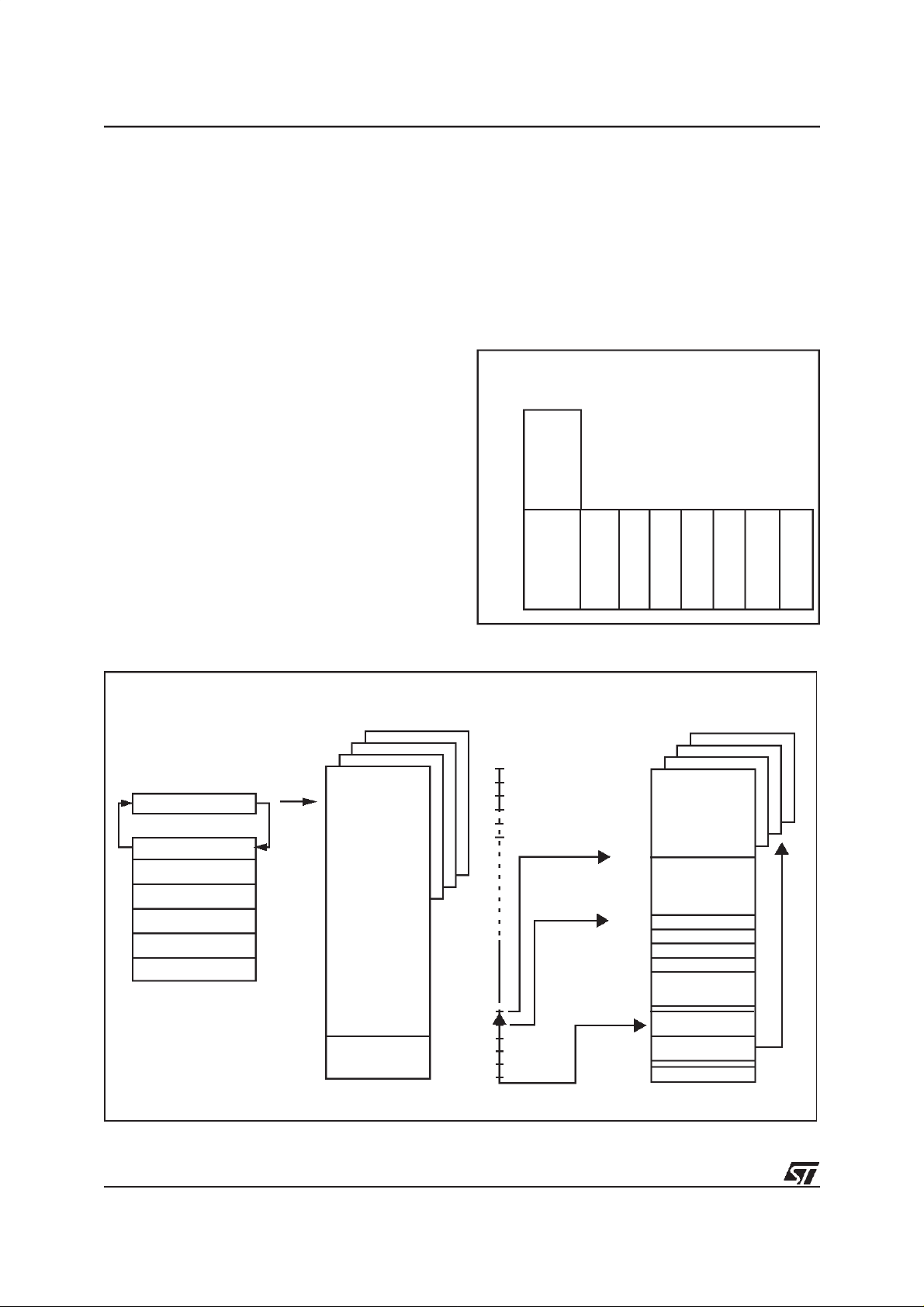
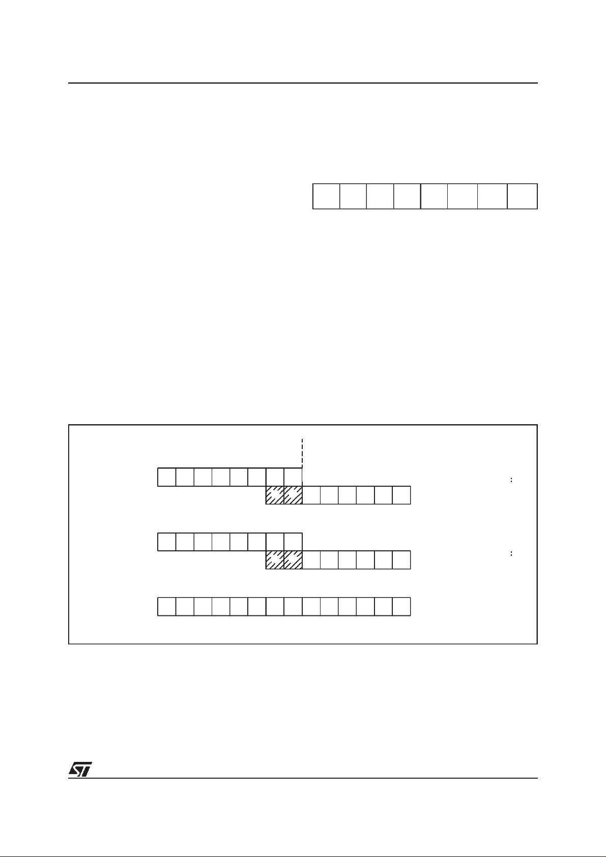
Figure 4. Memory Addressing Diagram
lower 2K byte of the 4K program space are bank
switched while the upper 2K byte can be seen as
static space. Table 3 gives the different codesthat
allows the selection of the corresponding banks.
Note that,from thememory point ofview, the Page
1 and the Static Page represent the same physical
memory: it is only a different way ofaddressing the
same location.
Figure 3.16K-Byte Program Space Addressing
Program
counter
space
0FFFh
0800h
07FFh
0000h
0000h
Static
Page
Page 1
Page 0
Page1
Static
Page
Page
Page Page Page Page Page
2345 67
1FFFh
PROGRAM COUNTER
STACK LEVEL 1
STACK LEVEL 2
STACK LEVEL 3
STACK LEVEL 4
STACK LEVEL 5
STACK LEVEL 6
0000h
0FF0h
RESET VECTORS
0FFFh
PROGRAM SPACE
ROM
INTERRUPT&
0-63
000h
03Fh
040h
07Fh
080h
081h
082h
083h
084h
0C0h
0FFh
DATA SPACE
RAM / EEPROM
BANKING AREA
DATA ROM
WINDOW
X REGISTER
Y REGISTER
V REGISTER
W REGISTER
RAM
DATA ROM
WINDOW SELECT
DATA RAM
BANK SELECT
ACCUMULATOR
8/64
MEMORY SPACES (Cont’d)
Program ROM Page Register (PRPR)
Address: CAh - Write only
Reset Value: XXh
70
- - - - - PRPR2 PRPR1 PRPR0
Care is required when handling the PRPR as it is
write only. For this reason, it is not allowed to
change the PRPR contents while executing interrupts drivers, asthe driver cannotsaveand thanrestore its previous content. Anyway, this operation
may be necessary if the sum of common routines
and interrupt drivers will take more than 2K bytes;
in this case could be necessary to divide theinterrupt driver in a (minor) partin the static page (start
D7-D3. These bits are not used but have to be
written to “0”.
PRPR2-PRPR0.
These are the program ROM
banking bits and the value loaded selects the corresponding page to be addressed in the lower part
of 4Kprogram address space as specified inTable
3.This register is undefined on reset.
Note:
Only the lower part of address space has been
bankswitched because interrupt vectors and common subroutines should be available all the time.
The reason of this structure is due to the fact that it
is not possible to jump from a dynamic page to another, unless jumping back to the static page,
changing contents of PRPR, and, then, jumping to
a different dynamic page.
and end), and in thesecond (major) part in one dynamic page.Ifitis impossible to avoid the writingof
this register in interrupts drivers, an image of this
register mustbesavedina RAM location, andeach
time the program writes the PRPR bit writes also
the image register. The image register must be
written first, so if an interrupt occurs between the
two instructions the PRPR is not affected.
Table 3.ProgramMemoryPageRegisterCoding
PRPR2 PRPR1 PRPR0 PC11 Memory Page
X X X 1 Static Page (Page 1)
0000Page0
0 0 1 0 Page 1 (Static Page)
0100Page2
0110Page3
1000Page4
1010Page5
1100Page6
1110Page7
ST6373
Table 4. ST6373 Program Memory Map
Program Memory Page Device Address Description
PAGE 0
PAGE 1
“STATIC”
PAGE 2
PAGE 3
PAGE 4
PAGE 5
PAGE 6
PAGE 7
0000h-007Fh
0080h-07FFh
0800h-0F9Fh
0FA0h-0FEFh
0FF0h-0FF7h
0FF8h-0FFBh
0FFCh-0FFDh
0FFEh-0FFFh
0000h-000Fh
0010h-07FFh
0000h-000Fh
0010h-07FFh
0000h-000Fh
0010h-07FFh
0000h-000Fh
0010h-07FFh
0000h-000Fh
0010h-07FFh
0000h-000Fh
0010h-07FFh
User ROM (End of 12K)
User ROM (End of 16K)
Note*): all reserved areas must be set to FFh in the ROM code.
*)
Reserved
User ROM
User ROM
Reserved
Interrupt Vectors
Reserved
NMI Vector
Reset Vector
Reserved
User ROM
Reserved
User ROM (End of 8K)
Reserved
User ROM
Reserved
Reserved
User ROM
Reserved
9/64

ST6373
MEMORY SPACES (Cont’d)
1.3.3 Data Space
The ST6 Coreinstruction set operates on a specific space, referred to as the Data Space, which
contains all the data necessary for the program.
Figure 5. Data Space
DATA RAM/EEPROM
BANK AREA
DATA ROM
WINDOWAREA
X REGISTER 080h
Y REGISTER 081h
V REGISTER 082h
W REGISTER 083h
DATA RAM
PORT A DATA REGISTER 0C0h
PORT B DATA REGISTER 0C1h
PORT C DATA REGISTER 0C2h
RESERVED 0C3h
PORT A DIRECTIONREGISTER 0C4h
PORT B DIRECTIONREGISTER 0C5h
PORT C DIRECTION REGISTER 0C6h
RESERVED 0C7h
INTERRUPT OPTIONREGISTER 0C8h
DATA ROM WINDOW REGISTER 0C9h
PROGRAM ROM PAGEREGISTER 0CAh
I C SPI DATA REGISTER 0CBh
DDC SPI DATA REGISTE R 0CCh
PORT A OPTION REGISTER 0CDh
PORT B OPTION REGISTER 0CEh
RESERVED 0CFh
ADC RE SULT REGISTER 0D0h
ADC CONTROL REGISTER 0D1h
TIMER 1 PRESCALERR EGISTER 0D2h
TIMER 1 COUNTER REGISTER 0D3h
TIMER 1 STATUS/CONTROL REGISTER 0D4h
TIMER 2 PRESCALERR EGISTER 0D5h
TIMER 2 COUNTER REGISTER 0D7h
WATCHDOG REGISTER 0D8h
000h
03Fh
040h
07Fh
084h
0BFh
*)
*)
The Data Space allows the addressing of RAM
(192 bytes), EEPROM (384 bytes plus 128 bytes
for the DDC SPI), ST6 Core and peripheral registers, as well as read-only data such as constants
and look-up tables.
MIRROR REGISTER 0D9h
TIMER 3 PRESCALERREGISTER 0DAh
TIMER 3 COUNTER REGISTER 0DBh
TIMER 3 STATUS/CONTROL REGISTER 0DCh
EVE NT COUNTER DATA REGISTER 1 0DDh
EVE NT COUNTER DATA REGISTER 2 0DEh
SYNC PROCESSOR CONTROL REGISTE R 0DFh
D/A 0/4 DATA CONTROL REGISTER 0E0h
D/A 1/5 DATA CONTROL REGISTER 0E1h
D/A 2/6 DATA CONTROL REGISTER 0E2h
D/A 3/7 DATA CONTROL REGISTER 0E3h
D/A 8 DATA CONTROL REGISTER 0E4h
I C SPI CONTROL REGISTE R 1 0E5h
I C SPI CONTROL REGISTE R 2 0E6h
D/A BA NK REGISTER 0E7h
DATA RAM BANK REGISTER 0E8h
DDC EEPROM CONTROL REGISTER 0E9h
EEPROM CO NTROL R EGISTER 0EAh
DDC SPI CONTROL REGISTER 1 0EBh
DDC SPI CONTROL REGISTER 2 0ECh
NMI/PWRIN/VSYNC INTERRU PT REGISTER 0EDh
HDA DATA REGISTER 1 0EEh
HDA DATA REGISTER 2 0EFh
PERIOD COUNTER DATA REGISTER 0F0h
PERIOD COUNTER 1 AND BLANK CTRLREG. 0F1h
AUTO-COU NTER REGISTER 0F2h
SCL LATCHAND DDC2B ADDRESSCTRL REG. 0F3h
XOR REGISTER 0F4h
RESERVED
ACCUMULATOR 0FFh
*)
*)
*)
*)
*)
*)
*)
*)
*)
*)
*)
*)
*)
0F5h
0FEh
*) These registers contain write only bits, in which
case the bit operation instructions are not possible.
10/64
MEMORY SPACES (Cont’d)
Data ROM Addressing.All the read-only data are
physically implemented in the ROM in which the
Program Space is also implemented. The ROM
therefore contains theprogram tobe executedand
also the constants and the look-up tables needed
for the program. The locations of Data Space in
which the different constants and look-up tables
are addressed by the ST6 Core can be considered
as being a 64-byte window through which it is possible to access to the read-only data stored in the
ROM. This window is located from the 40h address to the 7Fh address in the Dataspace and allows the direct reading of the bytes from the 000h
address to the 03Fh address in the ROM. All the
bytes of the ROM can be used to store either instructions or read-only data. Indeed, the window
can be moved by step of 64 bytes along the ROM
in writing the appropriate code in the Write-only
Data ROM Window register (DRWR, location
C9h). The effective address of the byte to be read
as a data in the ROM is obtained by the concatenation ofthe 6 less significant bits of the address in
the Data Space (as less significant bits) and the
content of the DRWR (as most significant bits). So
when addressing location 40h of data space, and
0 is loaded in the DRWR, the physical addressed
location in ROM is 00h.
Figure 6. Data ROM Window Memory Addressing
ST6373
Data ROM Window Register (DWR)
Address: C9h - Write only
Reset Value: XXh
70
DWR7 DWR6 DWR5 DWR4 DWR3 DWR2 DWR1 DWR0
DWR7-DWR0. These are the Data Rom Window
bits that correspond to the upper bits of data ROM
program space. Thisregister is undefined after reset.
Note:
Care is required when handling the DRWR as it is
write only. For this reason, it is not allowed to
change the DRWR contents while executing interrupts drivers, as the driver cannot save and than
restore its previous content. If it is impossible to
avoid the writing of this register in interrupts drivers, an image of this register must be saved in a
RAM location, and each time the program writes
the DRWR it writes also the image register. The
image register must be written first, so if an interrupt occurs between the two instructions the
DRWR register is not affected.
DATA ROM
WINDOW REGISTER
CONTENTS
(DWR)
Example:
DWR=28h
ROM
ADDRESS:A19h
13
12
7
65432 0
0
0
00000000
11
11
1
01
0
01
543210
67891011
543210
0000
1
1
0
11
00
1
PROGRAM SPACE ADDRESS
READ
DATA SPACE ADDRESS
40h-7Fh
IN INSTRUCTION
DATA SPACE ADDRESS
1
59h
VR01573B
11/64
ST6373
MEMORY SPACES (Cont’d)
1.3.4 Data RAM/EEPROM
In the ST6373, 64 bytes of data RAM are directly
addressable in the data space from 80h to BFh addresses. The additional 128 bytes of RAM, and the
384 + 128 bytes of EEPROM can be addressed
using the 64-byte banks located between addresses 00H and 3Fh. Bank selection is carried out by
programming the Data RAM Bank Register (DRBR) located at address E8h of the Data Space. In
this way each bank of RAM or EEPROM can select 64 bytes at a time. No more than one bank
should be set at a time.
Data RAM Bank Register (DRBR)
Address: E8h - Write only
Reset Value: XXh
70
DRBR7DRBR6DRBR5DRBR4DRBR3DRBR2DRBR1DRBR
DRBR6
. This bit is reserved and must be held at
0
“0”.
DRBR5, DRBR4
. Each of these bits,when set,will
select one page of the EEPROM dedicated to the
DDC SPI.
DRBR3, DRBR2
. Each of these bits,when set,will
select oneRAM page.
DRBR7, DRBR1, DRBR0. These bits select the
EEPROM pages.
This register isundefined after reset.
Table 5 summarizes how to set the Data RAM
Bank Register in order to select the various banks
or pages.
Note:
Care is required when handling the DRBR as it is
write only. For this reason, it is not allowed to
change the DRBR contents while executing interrupts drivers, as the driver cannot save and than
restore its previous content. If it is impossible to
avoid the writing of this register in interrupts drivers, an image of this register must be saved in a
RAM location, and each time the program writes
the DRBRit writes also the image register. The image register must be written first, so if an interrupt
occurs between the two instructions the DRBR is
not affected.
1.3.5 EEPROM Description
The data space of ST6373 devices, from 00h to
3Fh, is paged as described in Table 5. The 512
bytes of EEPROM are located in eight pages of 64
bytes (see Table 3 below).
Table 5. Data RAM Bank Register Set-up
DRBR Value
Hex. Binary
01h 0000 0001 EEPROM Page 0
02h 0000 0010 EEPROM Page 1
03h 0000 0011 EEPROM Page 2
04h 0000 0100 RAM Page 2
08h 0000 1000 RAM Page 3
10h 0001 0000 DDC EEPROM Page 0
20h 0010 0000 DDC EEPROM Page 1
81h 1000 0001 EEPROM Page 3
82h 1000 0010 EEPROM Page 4
83h 1000 0011 EEPROM Page 5
Selection
12/64

MEMORY SPACES (Cont’d)
By programming the Data RAM Bank Register,
DRBR, the user can select the bank or page leaving unaffected the means of addressing the static
registers. The way to address the “dynamic” page
is to set the DRBR as described in Table 5 (e.g. to
select EEPROM page 0,the DRBR has tobe loaded with content 01h, see Data RAM/EEPROM addressing for additional information). Bits 0,1 and
4,5,7 of the DRBR are dedicated to the standard
EEPROM and DDC EEPROM respectively.
The EEPROM pages do not require dedicated instructions to be accessed in reading or writing.
The standard EEPROM is controlled by the EEPROM Control Register, EECR, the DDC EEPROM
is controlled by the DDC EPROM Control Register
DEECR, in the same way. Any EEPROM location
can be read just like any other data location, also
in terms of access time.
To write an EEPROM location takes an average
time of 5ms and during this time the EEPROM is
not accessible by the Core. A busy flag can be
read by the Core to know the EEPROM status before trying any access. In writing the EEPROM can
work in two modes: Byte Mode (BMODE) and Parallel Mode (PMODE). TheBMODE is the normal
way to use the EEPROM and consists in accessing one byteat a time. The PMODE consists in accessing 8 bytes per time.
SB. WRITE ONLY. If this bit is setthe EEPROM is
disabled (any access will be meaningless) and the
power consumption of theEEPROM is reduced to
the leakage values.
D5, D4. Reserved for testing purposes, they must
be set to zero.
PS
. SET ONLY. Once in Parallel Mode, as soon
as the user software sets the PS bit the parallel
writing of the 8 adjacent registers will start. PS is
internally reset at the end of the programming procedure. Note that less than 8 bytes can be written;
after parallel programming the remaining undefined bytes will have no particular content.
PE. WRITEONLY. This bit must be setbythe user
program in order to perform parallel programming
(more bytes per time). IfPE is setand the “parallel
start bit” (PS) is low, up to 8 adjacent bytes can be
written at the maximum speed, the content being
stored in volatile registers. These 8 adjacent bytes
can be considered as row, whose A7, A6, A5, A4,
A3 are fixed while A2, A1 and A0 are the changing
bytes. PE is automatically reset at the end of any
parallel programming procedure. PE can be reset
by the user software before starting the programming procedure, leaving unchanged the EEPROM
registers.
BS. READ ONLY.This bit willbe automatically set
by the CORE when the user program modifies an
EEPROM register. The user program has to test it
EEPROM Control Register (EECR)
Address: EAh - Read/Write
Reset Value: 00h
70
Re-
-SB
served
Re-
served
PS PE BS EN
DDC EEPROM Control Register (DDCEECR)
Address: E9h - Read/Write
Reset Value: 00h
70
Re-
-SB
D7
. Not used
served
Re-
served
PS PE BS EN
before any read or write EEPROM operation; any
attempt to access the EEPROM while “busy bit” is
set will be aborted and the writing procedure in
progress completed.
EN
. WRITE ONLY. This bit MUST be set to one in
order to write any EEPROM register. If the user
program will attempt to write the EEPROM when
EN= “0” the involved registers will be unaffected
and the “busy bit” will not be set.
Notes
:
When the EEPROM is busy (BS = “1”) the EECR
cannot be accessed in write mode, it is only possible to read BS status.This implies that, as long as
the EEPROM is busy, it is not possible to change
the status of the EEPROM control register. EECR
bits 4 and 5 are reserved for test purposes, and
must never be set.
ST6373
13/64

ST6373
MEMORY SPACES (Cont’d)
Additional Notes on Parallel Mode. If the user
wants to perform a parallel programming the first
action should be the setting of the PE bit; from this
moment, the first time the EEPROM will be addressed in writing, the ROW address will be
latched and it will be possible to change it only at
the end of the programming procedure or by resetsetting PE without programming the EEPROM.
After the ROW address latching the Core can
“see” just one EEPROM row (the selected one)
and any attempt to write or read other rows will
produce errors. Do not read the EEPROM while
PE is set.
As soon as PE bit is set, the 8 volatile ROW latches are cleared. From this moment the user can
load data in the wholeROW or just in a subset. PS
setting will modify the EEPROM registers corresponding to the ROW latches accessed after PE.
For example, ifthe software sets PE and accesses
EEPROM in writing at addresses 18h,1Ah,1Bh
and then sets PS, these three registers will be
modified at thesame time;the remaining bytes will
have no particular content. Note that PE is internally reset at the end of the programming procedure. This implies that the user must set PE bit between two parallel programming procedures. Anyway the user can set and then reset PE without
performing any EEPROM programming. PS is a
set only bit and is internally resetat the end of the
programming procedure. Note that if the user tries
to set PS while PE is not set there will not be any
programming procedure and the PS bit will be unaffected. Consequently PS bit can not be set if EN
is low. PS can be affected by the user set if, and
only if, EN and PE bits are also set to one.
14/64

1.4 MEMORY PROGRAMMING
ST6373
1.4.1 Program Memory
The ST6373 OTP and EPROM MCUs can be programmed with a range of EPROM programming
tools available from SGS-THOMSON.
EPROM/OTP programming mode is set by a
+12.5V voltage applied to the TEST/VPPpin. The
programming flow is described in the User Manual
of the EPROM Programming Tool.
1.4.2 Option Byte
The Option Byte allows OTP and EPROM versions to be configured to offer the same features
available as mask options in ROM devices. The
Option Byte’s content is automatically read, and
the selected options enabled on Reset.
The Option Byte can onlybe accessed during programming mode. Access is either automatic (copy
from a master device) or by selecting the OPTION
BYTE PROGRAMMING mode ofthe programmer.
The option byte is located in a non-user map. No
address needs to be specified.
Option Byte
0 = 100KHz (default)
1 = 400KHz
All other bits must be programmed asshown in the
register table above.
The Option byte is written during programming ei-
ther by using the PC menu (PC driven Mode) or
automatically (stand-alone mode).
1.4.3 Eprom Erasure
Thanks to the transparent window present in the
EPROM package, its memory contents may be
erased by exposure to UV light.
Erasure begins when thedevice is exposed to light
with a wavelength shorter than 4000Å. It should be
noted that sunlight, as well as some types of artificial light, includes wavelengths in the 3000-4000Å
range which, on prolonged exposure, can cause
erasure of memory contents. It is thus recommended that EPROM devices be fitted with an
opaque label over the window area in order to prevent unintentional erasure.
The recommended erasure procedure forEPROM
devices consists of exposure to short wave UV
light having a wavelength of 2537Å. The minimum
70
recommended integrated dose (intensity x exposure time) for complete erasure is 15Wsec/cm2.
0000X 010
This is equivalent to an erasure time of 15-20 minutes using a UV source having an intensity of
12mW/cm2at a distance of 25mm (1 inch) from
bit 3 =
I2C Clock Speed
:
the device window.
15/64
ST6373
2 CENTRAL PROCESSING UNIT
2.1 INTRODUCTION
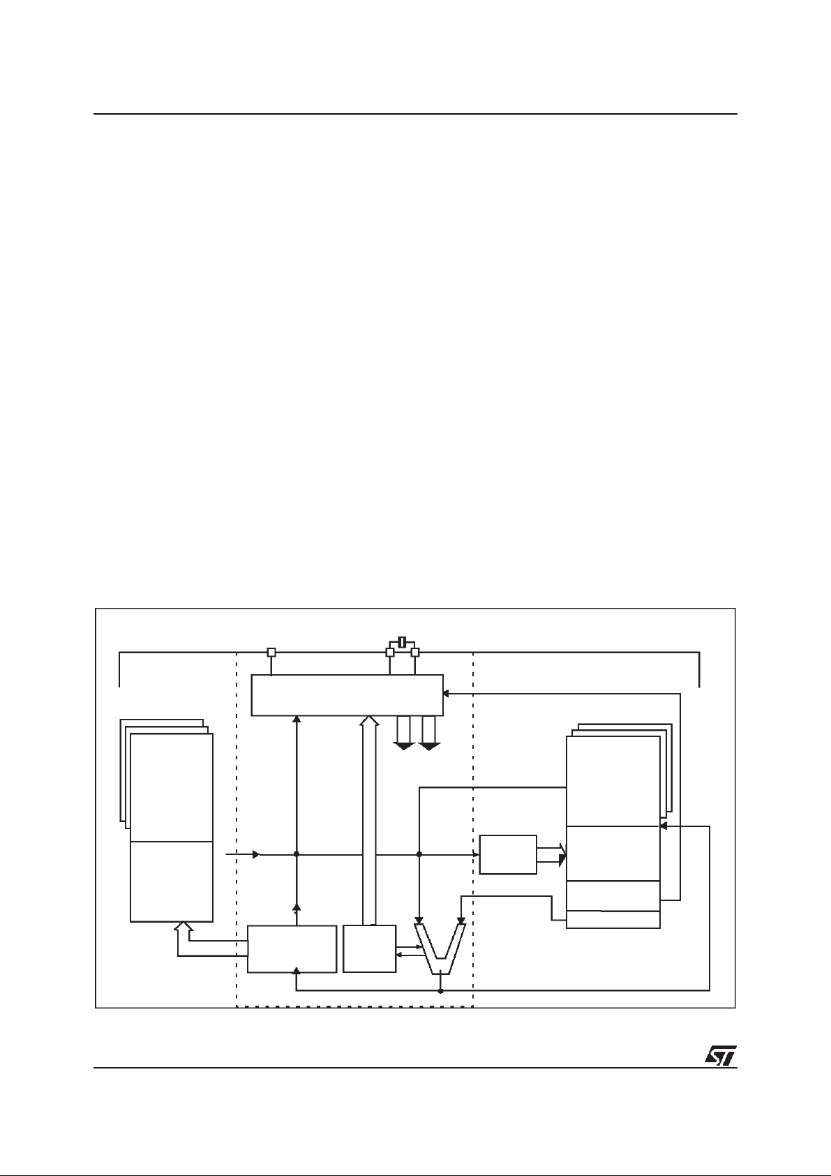
The CPU Core ofST6devicesisindependent ofthe
I/O or Memory configuration. As such, it may be
thought of as an independent central processor
communicating with on-chip I/O, Memory and Peripherals via internal address, data, and control
buses. In-core communication is arranged as
shown in Figure 1; the controller being externally
linked to both the Reset and Oscillator circuits,
while thecore islinked to the dedicatedon-chip peripherals via the serial data bus and indirectly, for
interrupt purposes, through the control registers.
2.2 CPU REGISTERS
The ST6 Family CPU core features six registers
and three pairs of flags available to the programmer. These are described in the following paragraphs.
Accumulator (A)
. The accumulator is an 8-bit
general purpose register used in all arithmetic calculations, logical operations, and data manipulations. The accumulator can be addressed in Data
space as a RAMlocation at address FFh. Thus the
ST6 can manipulate the accumulator just like any
other register in Data space.
Figure 7. ST6 Core Block Diagram
0,01 TO 8MHz
RESET
OSCin
Indirect Registers (X, Y).
These two indirect registers are used as pointers to memory locations in
Data space. They are used in the register-indirect
addressing mode. These registers can be addressed in thedata space as RAM locations at addresses 80h (X) and 81h (Y). They can also be accessed with the direct, short direct, or bit direct addressing modes. Accordingly, the ST6 instruction
set can use theindirect registers as any other register of the data space.
Short Direct Registers (V, W).
These two registers are used to save a byte in short direct addressing mode. They can be addressed in Data
space as RAM locations at addresses 82h (V) and
83h (W). They can also be accessed using the direct and bit direct addressing modes. Thus, the
ST6 instruction set can use the short direct registers as any other register of the data space.
Program Counter (PC). The program counter is a
12-bit register which contains the address of the
next ROM location to be processed by the core.
This ROM location may be an opcode, an operand, or the address of an operand. The 12-bit
length allows the direct addressing of 4096 bytes
in Program space.
OSCout
16/64
PROGRAM
ROM/EPROM
12
CONTROLLER
OPCODE
Program Counter
and
6 LAYER STACK
FLAG
VALUES
2
FLAGS
CONTROL
SIGNALS
A-DATA
ADDRESS/READ LINE
ADDRESS
DECODER
B-DATA
ALU
RESULTS TO DATA SPACE(WRITE LINE)
INTERRUPTS
256
DATA SPACE
DATA
RAM/EEPROM
DATA
ROM/EPROM
DEDICATIONS
ACCUMULATOR
VR01811
CPU REGISTERS (Cont’d)
However, if the program space contains more than
4096 bytes, the additional memory in program
space can be addressed by using the Program
Bank Switch register.
The PC value is incremented after reading theaddress ofthe current instruction. To executerelative
jumps, the PC and the offset are shifted through
the ALU, where they are added; the result is then
shifted back into the PC. The program counter can
be changed in the following ways:
- JP (Jump) instruction. . . . . PC=Jump address
- CALL instruction . . . . . ....PC=Calladdress
- Relative Branch Instruction. PC= PC +/- offset
- Interrupt . . . . . . . . . . . . . .PC=Interrupt vector
- Reset . ................PC=Reset vector
- RET & RETI instructions . .. . PC= Pop (stack)
- Normal instruction . . . . . . .......PC=PC+1
Flags (C, Z). The ST6 CPU includes three pairs of
flags (Carry and Zero), each pair being associated
with one of the three normal modes of operation:
Normal mode, Interrupt mode and Non Maskable
Interrupt mode. Each pair consists of a CARRY
flag and a ZERO flag. One pair (CN, ZN) is used
during Normal operation, another pair is used during Interrupt mode (CI, ZI),and a third pair is used
in the Non Maskable Interrupt mode (CNMI, ZNMI).
The ST6 CPU uses the pair of flags associated
with the current mode: as soon as an interrupt (or
a Non Maskable Interrupt) is generated, the ST6
CPU uses the Interrupt flags (resp. the NMI flags)
instead of the Normal flags. When the RETI instruction is executed, the previously used set of
flags is restored. It should be noted that each flag
set can only be addressed in its own context (Non
Maskable Interrupt, Normal Interrupt or Main routine). The flags are not cleared during context
switching andthus retain their status.
The Carry flag is set when a carry or a borrow occurs during arithmetic operations; otherwise it is
cleared. The Carry flag is also set to the value of
the bit tested in a bit test instruction; it also participates in the rotate left instruction.
The Zero flag is set if the result of the lastarithmetic or logical operation was equal to zero; otherwise it is cleared.
Switching between the three sets of flags is performed automatically when an NMI, an interrupt or
a RETI instructions occurs. As the NMI mode is
ST6373
automatically selected after the reset of the MCU,
the ST6 core uses at first the NMIflags.
Stack.
ware stack which eliminates the need for a stack
pointer. The stack consists of six separate 12-bit
RAM locations that do not belong to the data
space RAM area. When a subroutine call (or interrupt request) occurs,the contents ofeach level are
shifted into the next higher level, while the content
of the PC is shifted into the first level (the original
contents of the sixth stack level are lost). When a
subroutine or interrupt return occurs (RET or RETI
instructions), the first level register is shifted back
into the PC and the value of each level is popped
back into the previous level. Since the accumulator, in common with all other data space registers,
is not stored in this stack, management of these
registers should be performed within the subroutine. The stack will remain in its “deepest” position
if morethan 6 nested calls or interrupts areexecuted, and consequently the last return address will
be lost. It will also remain in its highest position if
the stack is empty and a RET or RETI is executed.
In this case the next instruction will be executed.
Figure 8. ST6 CPU Programming Mode
l
The ST6 CPU includes a true LIFO hard-
X REG. POINTER
INDEX
REGISTER
INTERRUPTFLAGS
NMI FLAGS
b7
b7
b7
b7
b7
PROGRAMCOUNTER
SIX LEVELS
STACKREGISTER
YREG.POINTER
VREGISTER
WREGISTER
ACCUM ULATOR
b0
b0
b0
b0
b0
b0b11
CZNORMAL FLAGS
CZ
CZ
SHORT
DIRECT
ADDRESSING
MODE
VA000 423
17/64
ST6373
3 CLOCKS, RESET, INTERRUPTS AND POWERSAVING MODES
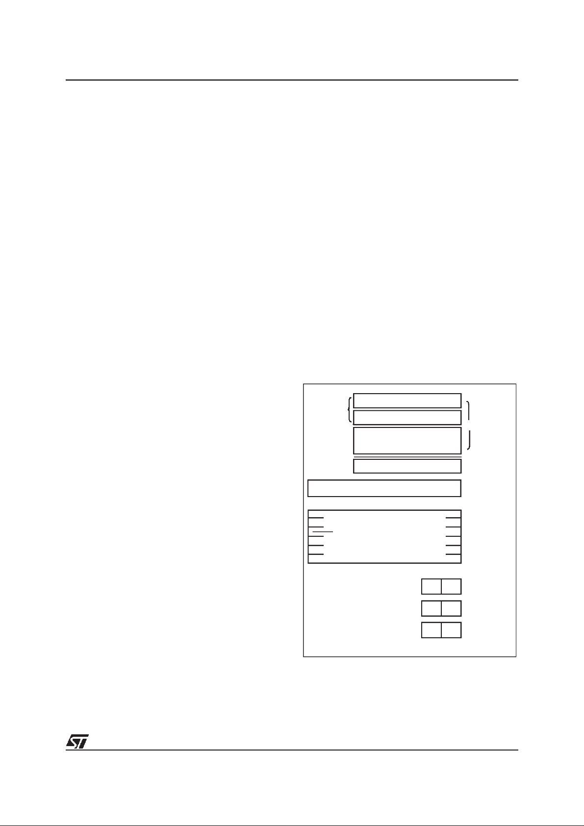
3.1 ON-CHIP CLOCK OSCILLATOR
The internal oscillator circuit is designed to require
a minimum of external components. A crystal
quartz, a ceramic resonator, or an external signal
(provided to the OSCin pin) may be used to generate a system clockwith various stability/cost tradeoffs. The typical clock frequency is 8MHz. Please
note that different frequencies will affect the operation of those peripherals (D/As, SPI) whose reference frequencies are derived from the system
clock.
The different clock generator connection schemes
are shown inFigure 1 and 2. One machine cycle
takes 13 oscillator pulses; 12 clock pulses are
needed to increment the PC while and additional
13th pulse is needed to stabilize the internal latches during memory addressing. This means that
with a clock frequency of 8MHz the machine cycle
is 1.625µSec.
The crystal oscillator start-up time is a function of
many variables: crystal parameters (especially
RS), oscillator load capacitance (CL), IC parameters, ambient temperature, and supply voltage.It
must be observed thatthe crystal or ceramic leads
and circuit connections must be as short as possible. Typical values for CL1 and CL2 are in the
range of 15pF to 22pF but these should be chosen
based on the crystal manufacturers specification.
Typical input capacitance for OSCin and OSCout
pins is 5pF.
The oscillatoroutput frequency is internally divided
by 13 to produce the machine cycle and by 12 to
produce the Timers and the Watchdog clock. A
byte cycle is the smallest unit needed to execute
any operation (i.e., increment the program counter). An instruction may need two, four, or five byte
cycles to be executed (SeeTable 1).
Table 6. Instruction Timing with 8MHz Clock
Figure 9. Clock Generator Option 1
CRYSTAL/RESONATOR CLOCK
ST6xxx
OSC
C
L1
OSC
in
out
C
L2
VA0016B
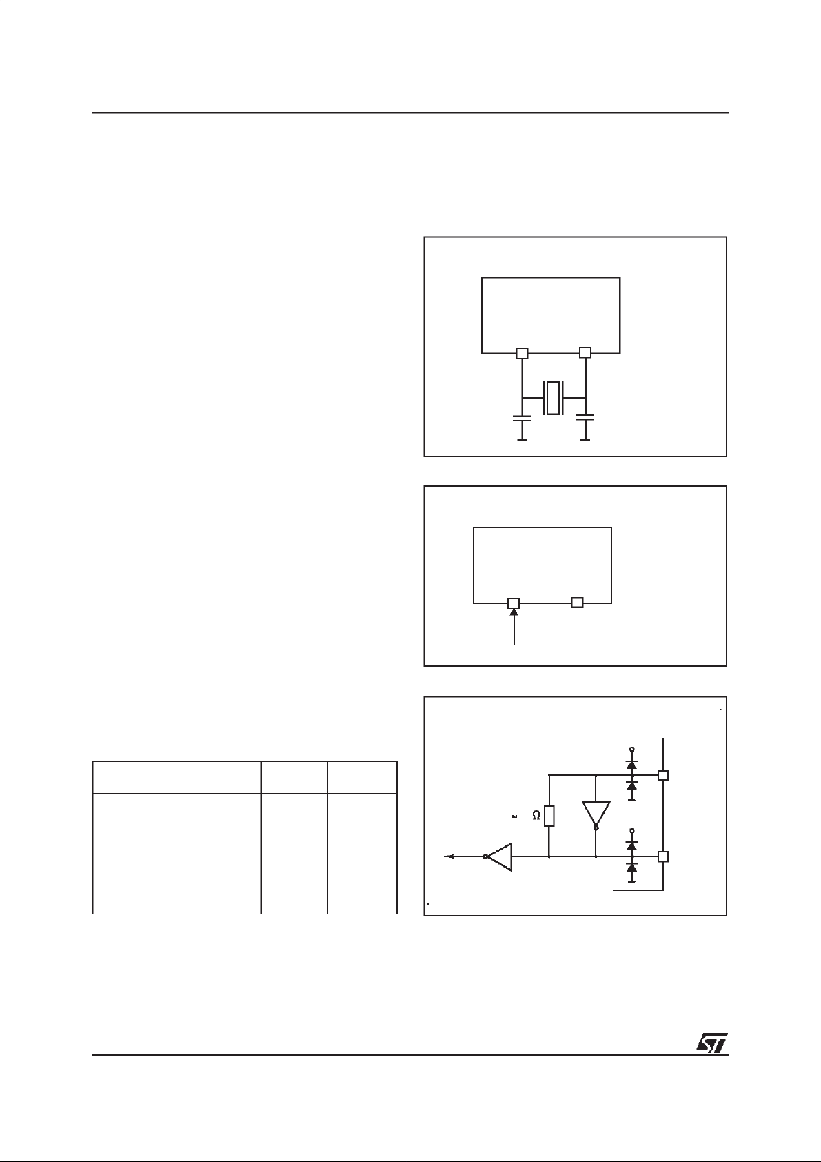
Figure 10. Clock Generator Option 2
EXTERNAL CLOCK
ST6xxx
OSC
OSC
in
out
NC
VA0015C
Figure 11. OSCin, OSCout Diagram
OSCin, OSCout (QUARTZ PINS)
V
DD
Instruction Type Cycles
Branch if set/reset 5 Cycles 8.125µs
Branch & Subroutine Branch 4 Cycles 6.50µs
Bit Manipulation 4 Cycles 6.50µs
Load Instruction 4 Cycles 6.50µs
Arithmetic & Logic 4 Cycles 6.50µs
Conditional Branch 2 Cycles 3.25µs
Program Control 2 Cycles 3.25µs
18/64
Execution
Time
OSCin
1M
In
V
DD
OSCout
VA00462
3.2 RESETS
ST6373
The MCU can be reset in three ways:
– by the external Reset input being pulled low;
– by Power-on Reset;
– by the digital Watchdog peripheral timing out.
3.2.1 RESET Input
The RESET pin may be connected to a device of
the application board in order to reset the MCU if
required. The RESET pin may be pulled low in
RUN, WAIT or STOP mode. This input can be
used to reset the MCU internal state and ensure a
correct start-up procedure. The pin is active low
and features a Schmitt trigger input. The internal
Reset signal is generated by adding a delay to the
external signal. Therefore even short pulses on
the RESET pin are acceptable, provided VDDhas
completed its rising phase and that the oscillatoris
running correctly (normal RUN or WAIT modes).
The MCU is kept in the Reset state as long as the
RESET pin is held low.
If RESET activation occurs in RUN or WAIT
modes, processing of the user program isstopped
(RUN mode only), theInputs and Outputs are configured as inputs with pull-up resistors if available.
When the level on the RESET pin then goes high,
the initialization sequence is executed following
expiry of the internal delay period.
If RESET pin activation occurs in the STOP mode,
the oscillator starts up and all Inputs and Outputs
are configured as inputs with pull-up resistors if
available. When the level of theRESET pin then
goes high, the initialization sequence is executed
following expiry of the internal delay period.
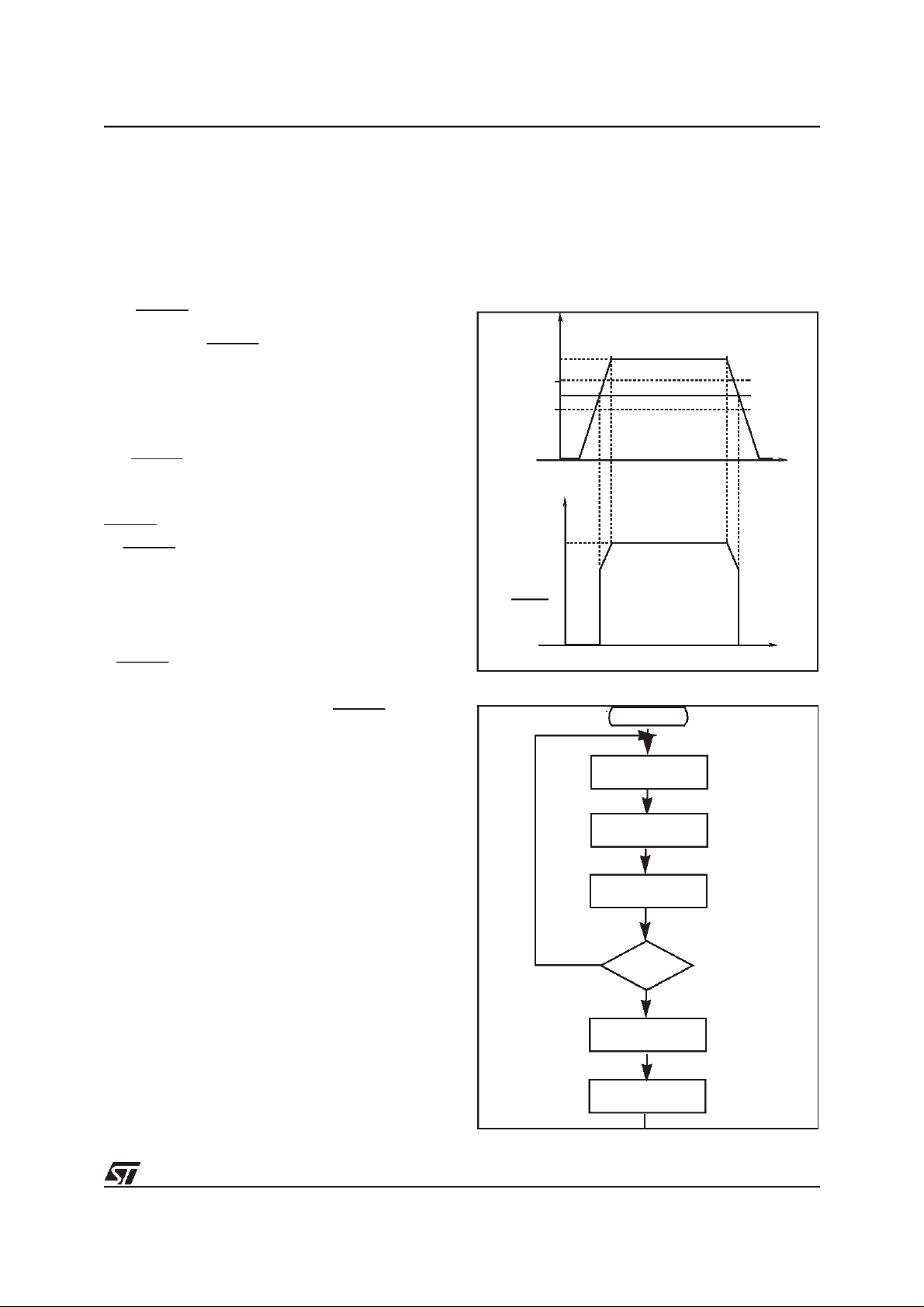
3.2.2 Power-on Reset
The function of the POR circuit consists in waking
up the MCU at an appropriate stage during the
power-on sequence. At the beginning of this sequence, the MCU is configured in the Reset state:
all I/O ports are configured as inputs with pull-up
resistors and noinstruction is executed. When the
power supply voltage rises to a sufficient level, the
oscillator starts to operate, whereupon an internal
delay is initiated, in order to allow the oscillator to
fully stabilize before executing the first instruction.
The initialization sequence is executed immediately following the internal delay.
The internal delay is generated by an on-chip
counter. Theinternal reset line is released 2048internal clock cycles after release of the external reset.
The internal POR device is a static mechanism
which forces the reset state when VDDis below a
threshold voltage in the range 3.4 to 4.2Volts (see
Figure 1).The circuit guarantees that the MCU will
exit or enter the reset state correctly, without spurious effects, ensuring, for example, that EEPROM
contents are not corrupted.
Note
: This featureisnot available on OTP/EPROM
Devices.
Figure 12. Power ON/OFF Reset operation
V
DD
4.2
Threshold
3.4
t
V
DD
POWER
ON/OFF
RESET
t
VR02037
Figure 13. Reset and Interrupt Processing
RESET
NMI MASK SET
INT LATCH CLEARED
( IF PRESENT )
SELECT
NMI MODE FLAGS
PUT FFEH
ON A DDRESSBUS
YES
IS RESET STILL
PRESENT?
NO
LOAD PC
FROM RESET LOCATION S
FFE/FFF
FETCH INSTRUCTION
VA000427
19/64
ST6373
RESETS (Cont’d)
3.2.3 Watchdog Reset
The MCU provides a Watchdog timer function in
order to ensure graceful recovery from software
upsets. If the Watchdog register is not refreshed
before an end-of-count condition is reached, the
internal reset will be activated. This, amongst other things, resets the watchdog counter.
The MCU restarts just as though the Reset had
been generated by theRESET pin, including the
built-in stabilisation delay period.
3.2.4 Application Note
No external resistor is required between VDDand
the Reset pin, thanks to the built-in pull-up device.
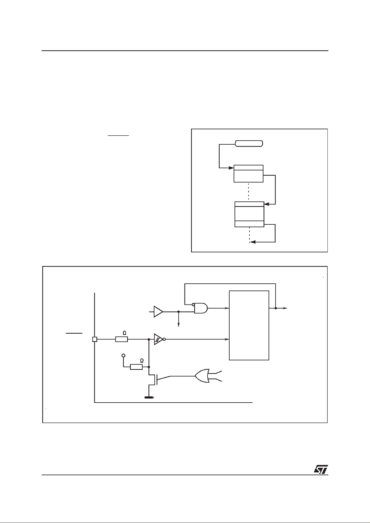
3.2.5 MCU Initialization Sequence
When a reset occurs the stack is reset, the PC is
loaded with the address of the Reset Vector (located in program ROMstarting at address 0FFEh). A
jump to the beginning of theuser program mustbe
coded at this address. Following a Reset, the Interrupt flag is automatically set, so that the CPU is
in Non Maskable Interrupt mode; this prevents the
initialisation routine from being interrupted. The initialisation routine should therefore be terminated
by a RETI instruction, in order to revert to normal
mode andenable interrupts. Ifno pending interrupt
is present at theend of the initialisation routine, the
MCU will continue by processing the instruction
immediately following the RETI instruction. If, however, a pending interrupt is present, it will be serviced.
Figure 14. Reset and Interrupt Processing
RESET
JP:2 BYTES/4CYCLES
RESET
VECTOR
INITIALIZATION
ROUTINE
JP
RETI: 1 BYTE/2 CYCLES
RETI
VA00181
Figure 15. Reset Circuit
RESET
(ACTIVE LOW)
OSCILLATOR
SIGNAL
1k
V
DD
300k
TO ST6
ST6
INTERNAL
RESET
COUNTER
RESET
WATCHDOG RESET
POWER ON/OFFRESET
VA0200E
20/64
 Loading...