

SGS Thomson Microelectronics ST63T69B1, ST6369B1, ST6369B, ST63E69D1 Datasheet

ST6369
DATA SHEET

USE INLIFE SUPPORTDEVICES OR SYSTEMS MUSTBE EXPRESSLYAUTHORIZED.
SGS-THOMSON PRODUCTS ARE NOT AUTHORIZED FOR USE AS CRITICAL COMPONENTS INLIFE SUPPORT DEVICES OR SYSTEMS WITHOUT THE EXPRESSWRITTEN APPROVAL OF SGS-THOMSON Microelectronics.
As used herein :
1. Life support devices or systems are those which (a) are
intended for surgical implant into the body, or (b) support
or sustain life, and whose failure to perform, when properly used in accordance with instructions for use provided with the product, can be reasonably expected to
result in significant injury to the user.
2. A criticalcomponent is any component of alife support
device or system whose failure to perform can reasonably be expected to cause the failure of the life support
device or system, or to affect its safety or effectiveness.

ST6369 DATASHEET INDEX
Pages
ST6369 ............................................. 1
GENERAL DESCRIPTION . . . . . . . . . . . . .......................... 2
PINDESCRIPTION ......................................... 4
ST6369 CORE . . . . . . . . . . . . . . . . . . . . . . . . . . . . . . . . . . . . . . . . . . . . 6
MEMORYSPACES . . . . . . . . . . . . . . . . . . ....................... 9
INTERRUPT . . . .......................................... 15
RESET . . . . . . . . . . . . . . . . . . . . . . . . . . . . . . . . . . . . . . . . . . . . . . . . 19
WAIT& STOPMODES . . . . . . . . . . . . . . . . ....................... 21
ON-CHIPCLOCK OSCILLATOR . . . . . . . . . . . . . . . . . . . . . . . . . . . . . . . . . . 22
INPUT/OUTPUT PORTS . . . . . . . . . . . . . . . . . . . . . . . . . . . . . . . . . . . . . . 23
TIMERS . . . . . . . . . . . . . . . . . . . . . . . . . . . . . . . . . . . . . . . . . . . . . . . 26
HARDWARE ACTIVATEDDIGITAL WATCHDOG FUNCTION . . . . . . ............. 29
SERIALPERIPHERALINTERFACE . . . . . . . . . . . . . . . . . . . . . . . . . . . . . . . . . 30
14-BITPWMD/A CONVERTER . . . . . . . . . . . . ....................... 39
6-BITPWMD/A CONVERTERS . . . . . . . . . . . . . . . . . . . . . . . . . . . . . . . . . . 40
A/D COMPARATOR . . . . . . . . . . . . . . . . . ........................ 40
DEDICATED LATCHES . . . . . . . . . . . . . . . . . . . . . . . . . . . . . . . . . ...... 42
SOFTWARE DESCRIPTION. . . . . ................................ 43
ABSOLUTEMAXIMUMRATINGS . . . . . . . . . . . . . . . . . . . . . . . . . . . . . . . . . . 48
PACKAGEMECHANICAL DATA . . . . . . . . . . . . . . . . . . . . . . . . . . . . . . . . . . 52
ORDERINGINFORMATION TABLE . . . . . . . . . . . . . . . . . . . . . ............ 53
ST63E69
ST63T69
............................................ 55
GENERAL DESCRIPTION . . . . . . . . . . . . .......................... 56
PINDESCRIPTION ......................................... 58
ST63E69,T69EPROM/OTPDESCRIPTION. . . . . . . . . . . . . . . . . . . . . . . . . . . . . 60
ABSOLUTEMAXIMUMRATINGS . . . . . . . . . . . . . . . . . . . . . . . . . . . . . . . . . . 61
ORDERINGINFORMATION . . . . . . . . . . . . . . . . . . . . . . . . . . . . . . . . . . . . 67

8-BIT HCMOS MCU FOR
D
IGITAL CONTROLLED MULTI FREQUENCYMONITOR
ST6369
4.5 to6V supply operatingrange
8MHzMaximum Clock Frequency
UserProgram ROM: 7948 bytes
Reserved Test ROM: 244 bytes
Data ROM: user selectable size
Data RAM: 256 bytes
Data EEPROM: 384 bytes
40-PinDual in Line Plastic Package
Up to 23 software programmable general pur-
pose Inputs/Outputs, including 2 direct LED
driving Outputs
Two Timerseach includingan 8-bit counter with
a 7-bitprogrammable prescaler
Digital WatchdogFunction
Serial Peripheral Interface(SPI)supporting
S-BUS/I
2
C BUSand standardserial protocols
One 14-BitPWM D/AConverter
Six 6-Bit PWM D/AConverters
One A/Dconverterwith 0.5V resolution
Five interrupt vectors(HSYNC/NMI,Timer1 &2,
VSYNC,PWR INT.)
On-chipclock oscillator
ST6369 is supported by pin-to-pin EPROMand
OTPversions.
The development tool of the ST6369 microcon-
troller consists of the ST6369-EMU emulation
and development system to be connectedvia a
standard RS232 serial line to an MS-DOSPersonal Computer.
This is Preliminary information from SGS-THOMSON. Details are subject tochange withoutnotice.
February 1993
(Ordering Information at the end of the datasheet)
1
PDIP40
PRELIMINARY DATA
DEVICE
ROM
(Bytes)
RAM
(Bytes)
EEPROM
(Bytes)
D/A
Conv.
ST6369 8K 256 384 7
DEVICE SUMMARY
1/67
V
DD
PC0 ( SCL )
PC1 ( SDA )
PC2
PC3 ( SEN )
PC4 ( PWRIN )
PC5
PC6 ( HSYNC )
PC7
RESET
OSCOUT
OSCIN
HDA
TEST
VSYNC
N.C.
N.C.
O0
O1
SS
V
DA1
DA0
DA2
DA3
DA4
DA5
PB1
PB2
AD
PB4
PB5
PB6
PA0
PA1
PA2
PA3
PA4
PA5
PA6 ( HD0 )
PA7 ( HD1 )
40
39
38
37
36
35
34
33
32
31
30
29
28
27
26
25
24
23
22
21
20
19
18
17
16
15
14
13
12
11
10
7
9
8
6
5
4
3
2
1
VR0G1375
ST6369
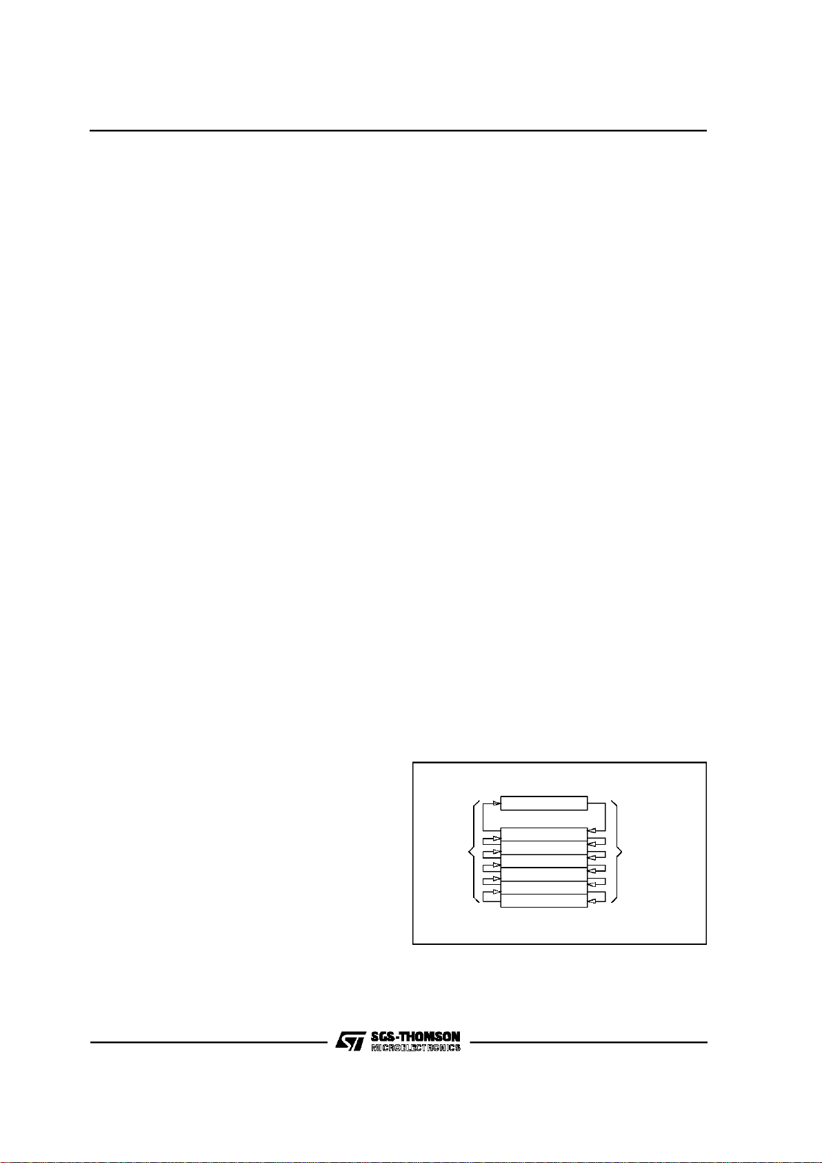
Figure1. ST6369 Pin Configuration GENERAL DESCRIPTION
The ST6369 microcontroller is member of the 8-bit
HCMOSST638xfamily,a seriesofdevicesspecially
orientedtoDigitalControlled MultiFrequencyMonitor applications. ST6369members are based on a
building block approach: a common core is surrounded by a combination of on-chip peripherals
(macrocells)availablefromastandardlibrary.These
peripheralsare designed with the same Core technology providing full compatibility and short design
time. Many of these macrocells are speciallydedicated to DCMF Monitor applications. The macrocellsof the ST6369 are: twoTimer peripheralseach
includingan 8-bitcounterwith a 7-bit software programmableprescaler(Timer), a digitalhardwareactivatedwatchdogfunction(DHWD), a 14-bitvoltage
synthesistuningperipheral,aSerialPeripheralInterface (SPI), six 6-bit PWM D/A converters, an A/D
converter with 0.5V resolution, a 14-bit PWM D/A
converter. In addition the following memory resources are available: program ROM (8K bytes),
dataRAM (256bytes),EEPROM (384bytes).
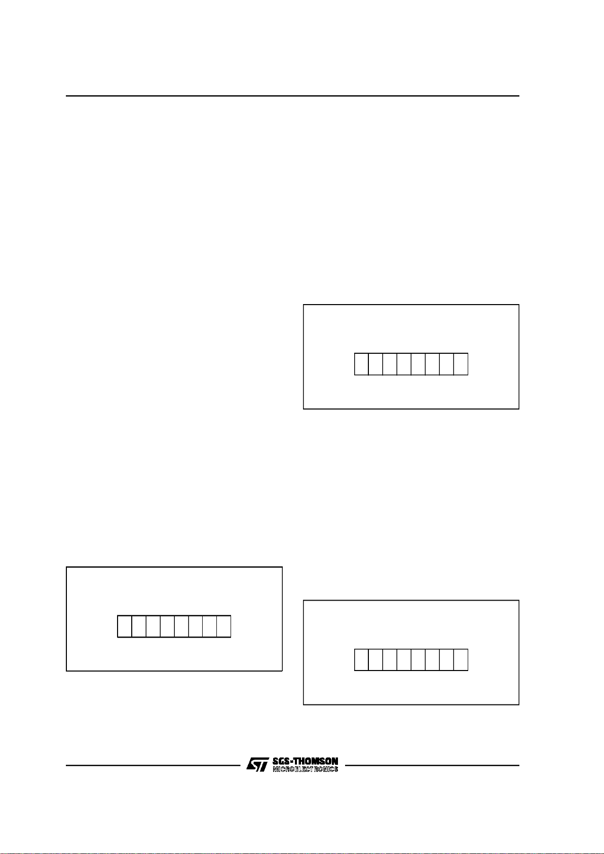
ST6369
2/67
STACK LEVEL 1
STACK LEVEL 2
STACK LEVEL 3
STACK LEVEL 4
STACK LEVEL 5
STACK LEVEL 6
PC
D/AOutputs
TIMER 2
INTERRUPT
Inputs
TEST
TIMER 1
PORT C
PORT B
PORT A
A/D Input
DIGITAL
WATCHDOG/TIMER
SERIAL PERIPHE RAL
INTERFACE
V
DD
V
SS
OSCin OSCout
RESET
VR0B1 753
PA0 PA7 *
HDA,DA0 DA5
HSYNC/PC6
VSYNC
TEST
AD
PB0 PB7 *
PC2,PC4 PC7 *
PC0 / SCL
PC1 / SDA
PC3 / SEN
POWER SUPPLY OSCILLATOR RESET
8-BIT CORE
USER PROGRAM
ROM
8 kBytes
DATA ROM
USER SELECTABLE
DATA EEPROM
384 Bytes
DATA RAM
256 Bytes
* Refer To Pin Configuration For Additional Information
Figure2. ST6369 Block Diagram
DEVICE
ROM
(Bytes)
RAM
(Bytes)
EEPROM
(Bytes)
A/D
14-bit
D/A
6-bit
D/A
EMULATING
DEVICES
ST6369 8K 256 384 1 1 6 ST63E69, ST63T69
Table 1. Device Summary
ST6369
3/67

PIN DESCRIPTION
V
DD
andVSS. Power issupplied to the MCU using
these twopins. V
DD
ispower and VSSistheground
connection.
OSCIN, OSCOUT. These pins are internally con-
nected to the on-chip oscillator circuit. A quartz
crystal or a ceramic resonator can be connected
between these two pins in order to allow the correct operation of the MCU with various stability/costtrade-offs. The OSCIN pin isthe input pin,
the OSCOUTpin is the output pin.
RESET. The activelow RESET pin is used to start
the microcontrollerto the beginning ofits program.
Additionally the quartz crystal oscillator will be disabled when theRESET pin islow to reduce power
consumption duringreset phase.
TEST. The TEST pin mustbe held at V
SS
for nor-
mal operation.
PA0-PA7. These 8 linesare organizedas oneI/O
port (A). Eachline may be configuredas either an
input withor withoutpull-upresistor or as an output
under softwarecontrol of the datadirectionregister. PinsPA4 toPA7 are configured as open-drain
outputs (12V drive). On PA4-PA7 pins the input
pull-up option is not available while PA6 and PA7
have additional current driving capability (25mA,
V
OL
:1V).PA0 to PA3pins areconfigured as push-
pull.
PB1-PB2, PB4-PB6. These 5 linesare organized
as one I/O port (B).Each line may be configuredas
either aninput withorwithoutinternalpull-up resistor or as an output under software control of the
data directionregister.
PC0-PC7. These 8 lines are organized as oneI/O
port (C). Each line may be configured as either an
input with or without internal pull-up resistoror as
an output under softwarecontrol of thedata direction register. Pins PC0 to PC3 are configured as
open-drain(5V drive)in output mode while PC4 to
PC7 are open-drain with 12V drive and the input
pull-up options does not exist on these four pins.
PC0, PC1 and PC3 lines when in output mode are
“ANDed” with the SPI control signals and are all
open-drain.PC0is connected to the SPI clock signal (SCL), PC1 with the SPI data signal (SDA)
while PC3 is connected with SPI enable signal
(SEN, used in S-BUSprotocol). Pin PC4 and PC6
can also be inputstosoftwareprogrammableedge
sensitive latches which can generate interrupts;
PC4 can be connected to Power Interrupt while
PC6 can be connected to the HSYNC/NMI interrupt line.
DA0-DA5. These pins are the six PWM D/A outputs of the 6-bit on-chip D/A converters. These
lines have open-drain outputs with 12V drive. The
output repetition rate is 31.25KHz (with 8MHz
clock).
AD. This is the input of the on-chip 10 levelscomparator that can be used to implement the Analog
Keyboard function. This pin is an highimpedance
input able to withstand signals with a peak amplitude upto 12V.
VSYNC. This is the Vertical Synchronization pin.
This pinis connected to an internal timer interrupt.
O0,O1. Thesetwo lines are outputopen-drain pins
with 12Vdrive.
HDA. This is the output pin of the on-chip 14-bit
PWMD/A Converter.This line isapush-pulloutput
with standarddrive.
ST6369
4/67

Pin Function Description
DA0 to DA5 Output, Open-Drain, 12V
AD Input,High Impedance, 12V
HDA Output, Push-Pull
VSYNC Input, Pull-up, Schmitt Trigger
TEST Input, Pull-Down
OSCIN Input, Resistive Bias,Schmitt Triggerto Reset Logic Only
OSCOUT Output,Push-Pull
RESET Input, Pull-up, Schmitt Trigger Input
PA0-PA3 I/O, Push-Pull, Software Input Pull-up, Schmitt Trigger Input
PA4-PA5 I/O, Open-Drain, 12V,No Input Pull-up, Schmitt Trigger Input
PA6-PA7 I/O, Open-Drain, 12V,No Input Pull-up, Schmitt Trigger Input, High Drive
PB1-PB2 I/O, Push-Pull, Software Input Pull-up, Schmitt Trigger Input
PB4-PB6 I/O, Push-Pull, Software Input Pull-up, Schmitt Trigger Input
PC0-PC3 I/O, Open-Drain,5V , SoftwareInput Pull-up,Schmitt Trigger Input
PC4-PC7 I/O, Open-Drain,12V, No Input Pull-up, Schmitt Trigger Input
O0, O1 Output, Open-Drain, 12V
V
DD,VSS
Power Supply Pins
Table 2. Pin Summary
ST6369
5/67
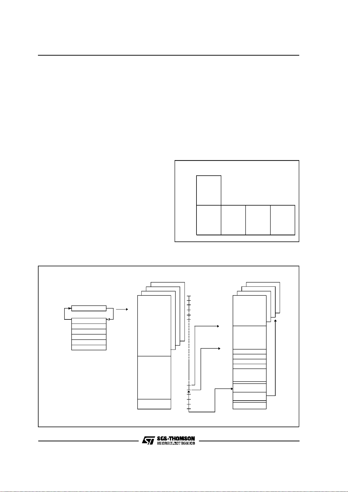
ST6369 CORE
The Core of the ST6369 is implemented independently from the I/O or memory configuration.
Consequently,it can betreatedas an independent
centralprocessorcommunicatingwithI/Oandmemoryvia internaladdresses,data,andcontrolbusses.
The in-core communication is arranged as shown
in the followingblock diagram figure; the controller
being externallylinkedto both thereset and the oscillator, while the core is linked to thededicatedonchip macrocells peripherals via the serial data bus
and indirectly for interrupt purposes through the
control registers.
Registers
The ST6369 Core has five registers and three
pairs of flags available to the programmer. They
are shown in Figure 4 and are explainedin the following paragraphstogether with the program and
data memorypage registers.
Accumulator (A). The accumulator is an 8-bit
general purpose register used in all arithmeticcalculations, logical operations, and data manipulations. The accumulator is addressed in the data
space asRAM locationat the FFH address.
Accordingly, the ST6369 instruction set can use
the accumulatoras anyother register of the data
space.
Figure3. Core Block Diagram
SHORT
DIRECT
ADDRESSING
MODE
V REGISTER
W REGISTER
PROGRAMCOUNTER
SIX LEVELS
STACKREGISTER
C
C
C
Z
Z
Z
NORMAL FLAGS
INTERRUPT FLAGS
NMI FLAGS
INDEX
REGISTER
VA000423
b7
b7
b7
b7
b7
b0
b0
b0
b0
b0
b0b11
ACCUMULATOR
Y REG. POINTER
X REG. POINTER
Figure4. Core ProgrammingModel
ST6369
6/67
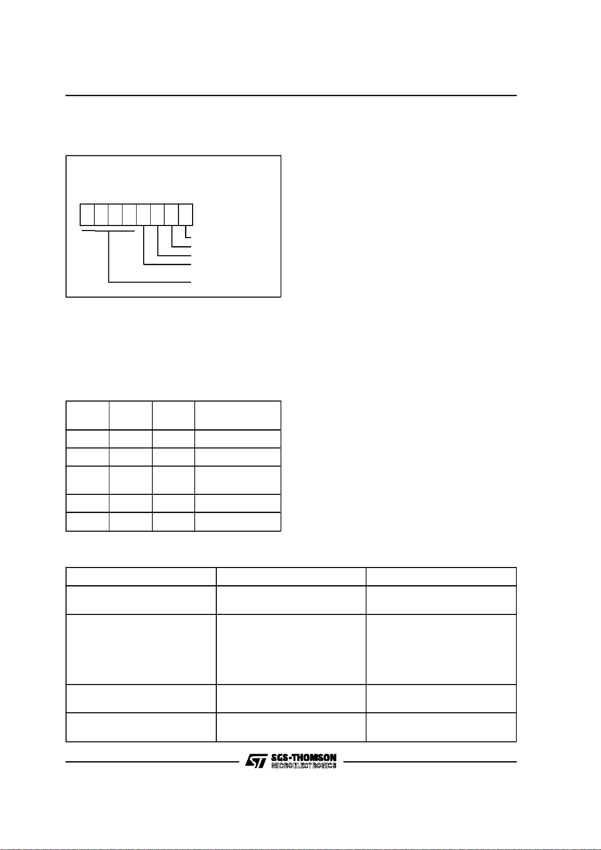
ST6369 CORE(Continued)
Indirect Registers (X, Y). These two indirect reg-
istersare usedas pointers tothe memorylocations
in the dataspace. They are usedin theregister-indirect addressing mode.These registers can be
addressed in the data space as RAM locations at
the 80H(X)and 81H (Y) addresses.They can also
be accessed with the direct, short direct, or bit direct addressing modes. Accordingly, the ST638x
instructionsetcan use the indirect registers as any
other registerof the data space.
Short Direct Registers (V, W). These two registers are used to save one byte in short direct addressing mode.These registerscan be addressed
in the data spaceas RAM locationsat the82H (V)
and 83H (W) addresses. They can also be accessed with the direct and bit direct addressing
modes. Accordingly, the ST638x instruction set
can use the shortdirect registers as any other register ofthe data space.
Program Counter (PC)
The program counter is a 12-bit registerthat contains the address of the next ROM location to be
processed by thecore.This ROM locationmay be
an opcode, an operand, or an address ofoperand.
The 12-bit length allows the direct addressing of
4096 bytes in the program space. Nevertheless, if
the program space contains more than 4096 locations, thefurtherprogram spacecan be addressed
by using theProgramROMPage Register.The PC
value isincremented,after it is read forthe address
of the current instruction,by sendingit through the
ALU, so giving the address of the nextbyte in the
program.Toexecuterelativejumpsthe PCand the
offset values are shifted through the ALU, where
they will be added, and the result is shifted back
into the PC. The program countercan be changed
in thefollowingways:
JP (Jump)instruction....PC=Jump address
CALL instruction...........PC=Call address
Relative Branch
instructions...................PC=PC+offset
Interrupt........................PC=Interruptvector
Reset............................PC=Resetvector
RET &RETI instructions............PC=Pop (stack)
Normal instruction........PC=PC+1
WHEN CALL
OR
INTERRUPT REQUEST
OCCURS
STACK LEVEL 1
STACK LEVEL 2
STACK LEVEL 3
STACK LEVEL 4
STACK LEVEL 5
STACK LEVEL 6
PROGRAM COUNTER
WHEN
RET OR RETI
OCCURS
VA000424
Figure5. Stack Operation
Flags (C, Z)
The ST6369 Core includesthree pairsof flagsthat
correspondto 3 different modes:normalmode,interrupt mode and Non-Maskable-Interrupt-Mode.
Each pair consistsof a CARRY flag and a ZERO
flag. One pair (CN, ZN) is used duringnormal operation, one pair is used during the interruptmode
(CI,ZI)andone is usedduring thenot-maskableinterruptmode (CNMI, ZNMI).
The ST6369 Core uses the pair of flags that correspondsto the actualmode: as soon as an interrupt
(resp. a Non-Maskable-Interrupt) is generated,the
ST6369Core uses the interruptflags(resp.the NMI
flags)insteadofthenormalflags.Whenthe RETIinstructionis executed,the normalflags(resp.the interrupt flags) are restored if the MCU was in the
normalmode (resp.inthe interruptmode)beforethe
interrupt.Shouldbe observedthateach flag setcan
onlybe addressedin itsownroutine(Not-maskable
interrupt,normalinterruptormainroutine).Theinterruptflags arenot clearedduring the contextswitchingand so,they remainin thestatethey were at the
exitof the lastroutineswitching.
The Carry flag is set when a carry or a borrow occurs during arithmetic operations, otherwise it is
cleared. The Carry flag is also set to the value of
the bit tested in a bit test instruction, and participates in the rotate left instruction.
TheZeroflagissetif theresultofthelastarithmetic
or logical operation wasequal to zero, otherwise it
is cleared.
The switching between these three sets is automaticallyperformedwhen anNMI,an interrupt and
a RETI instructions occur. As the NMI mode is
automatically selected after the reset ofthe MCU,
the ST6369Core uses at first the NMI flags.
ST6369
7/67
ST6369 CORE (Continued)
Stack
The ST6369 Core includes true LIFO hardware
stack that eliminates the need fora stack pointer.
The stackconsists ofsixseparate12-bit RAMlocations that do not belong to the data space RAM
area. When a subroutine call (or interruptrequest)
occurs,the contentsofeach levelis shiftedinto the
next levelwhile the contentofthe PC is shiftedinto
the first level (the value of the sixth level will be
lost). When subroutine or interrupt return occurs
(RET or RETI instructions), the first levelregisteris
shifted back into the PCand thevalue of eachlevel
is shifted back into the previous level. These two
operating modes are describedin Figure 5. Since
the accumulator,as all otherdata space registers,
is notstored inthisstack the handling of thisregisters shall be performed inside the subroutine. The
stack pointer will remain in its deepest position,if
more than 6 calls or interrupts are executed, so
that the last return address will be lost. It will also
remain in its highest position if the stack is empty
and a RET or RETI is executed. In this case the
next instructionwill be executed.
Memory Registers
The PRPR can be addressed like a RAM location
in the Data Spaceat the CAH address; nevertheless it is a write-only register that can not be accessed with single-bit operations.This register is
used to select the 2-Kbyte ROM bank of the Program Spacethat will be addressed.The number of
the pagehastobe loaded inthePRPR.ThePRPR
is not cleared during the MCU initialization and
should thereforebe defined before jumpingout of
the static page. Refer to the Program Space description for additional information concerning the
use of this register. The PRPR is not modified
when an interruptor a subroutine occurs.
PRPR
Program ROMPage Register
(CAH, Write Only)
D7 D6 D5 D4 D3 D2 D1 D0
Figure6. Program ROMPage Register
DRBR
Data RAM Bank Register
(E8H, Write Only)
D7 D6 D5 D4 D3 D2 D1 D0
Figure7. Data RAM Bank Register
DRWR
Data ROM Window Register
(C9H, Write Only)
D7 D6 D5 D4 D3 D2 D1 D0
Figure8. Data ROM WindowRegister
The DRBR can be addressedlike a RAMlocation
in the Data Space at the E8H address, nevertheless it is write-only register that can not be accessed with single-bit operations. This register is
used to select the desired 64-byteRAM/EEPROM
bank of the Data Space. The numberof the bank
has to be loaded inthe DRBR and the instruction
has to point to the selected location as itwas inthe
0 bank (from 00H address to 3FH address). This
register is undefined afterReset. Refer to the Data
Space description for additional information. The
DRBR register is not modified when a interrupt or
a subroutine occurs.
TheDRWR registercanbeaddressedlike a RAMlocationintheDataSpaceattheC9Haddress,nevertheless it is write-only register that can not be
accessed with single-bit operations.This registeris
used to move up and down the 64-byte read-only
datawindow(from the 40H address to 7FHaddress
of the Data Space)along the ROM of the MCU by
stepof 64 bytes.Theeffectiveaddressof thebyteto
bereadasadata inthe ROMisobtainedbythe concatenationofthe6lesssignificantbitsoftheaddress
given in the instruction(as less significant bits)and
the content of the DRWR (as most significant
bits). Refer to the Data Space descriptionfor additionalinformation.
ST6369
8/67
MEMORY SPACES
The MCUs operate in three different memory
spaces: Stack Space, Program Space and Data
Space. A descriptionof these spaces is shown in
Figure 9.
Stack Space
Thestack spaceconsistsof six 12 bit registers that
areusedfor stackingsubroutineandinterrupt return
addressesplusthecurrentprogramcounterregister.
Program Space
The program space is physically implemented in
the ROM and includes all the instructionsthat are
to be executed, as well as the data requiredforthe
immediate addressing mode instructions, the reserved test area and uservectors. It is addressed
thanks to the 12-bit Program Counter register (PC
register) and so, the ST6369 Core can directlyaddress up to 4Kbytesof ProgramSpace.Nevertheless, the Program Space can be extended by
the addition of 2-KbyteROM banks as it is shown
in Figure 11 in which a 8K bytes memory is described.Thesebanks areaddressed bypointing to
the 000H-7FFH locations of the Program Space
thanks to the Program Counter, andby writingthe
appropriatecode in theProgram ROM Page Register (PRPR) located at the CAH address of the
Data Space.Becauseinterruptsand common sub-
PROGRAM SPACE
VR001568
INTERRUPT &
RESET VECTORS
ACCUMULATOR
WREGISTER
RAM
DATA ROM
WINDOW
RAM / EEPROM
BANKING AREA
DATA SPACE
DATA RAM
BANK SELECT
DATA ROM
WINDOW SELECT
VREGISTER
YREGISTER
XREGISTER
0-63
0000h
07FFh
0800h
0FF0h
0FFFh
000h
03Fh
040h
070h
080h
081h
082h
083h
084h
0FFh
0C0h
ROM
ROM
STACK LEVE L 1
STACK LEVE L 2
STACK LEVE L 3
STACK LEVE L 4
STACK LEVE L 5
STACK LEVE L 6
PROGRAM COUNTER
STACK SPACE
Figure9. Memory Addressing Description Diagram
routines should be availableall the time only the
lower 2K byte of the 4K programspace are bank
switched while the upper 2K byte can be seen as
static space. Table 3 gives thedifferent codes that
allows the selection of the corresponding banks.
Note that,fromthe memory point of view,thePage
1 and the StaticPage represent the same physical
memory:it isonly adifferentway ofaddressingthe
same location.
Program
counter
space
0000H 1FFFH
0FFFH
Static Page
Page 1
0800H
07FFH
Page 0
Page 1
Static Page
Page 2 Page 3
0000H
Figure10. 8K Bytes Program Space Addressing Description
ST6369
9/67
D7-D2.Thesebitsare not used but haveto bewritten to “0”.
PRPR1-PRPR0. These are the program ROM
banking bits and thevalue loaded selects the corresponding page to be addressedin the lower part
of 4Kprogramaddress spaceas specifiedin Table
3. Thisregisteris undefined onreset.
MEMORY SPACES(Continued)
Note. Only the lower part of address space has
been bankswitchedbecause interrupt vectors and
common subroutines should be available all the
time. The reason of this structureis dueto the fact
that it isnot possible to jumpfrom a dynamicpage
to another,unlessjumping back to the staticpage,
changingcontents of PRPR,and, then, jumping to
a differentdynamicpage.
Care is required when handlingthe PRPR as it is
write only. For this reason, it is not allowed to
change the PRPR contents while executing interrupts drivers, as the driver cannot save and than
restore its previous content. Anyway, this operation may be necessary if thesum ofcommon routines and interrupt driverswill take more than 2K
bytes; in this case could benecessaryto divide the
interrupt driver in a (minor) part in the static page
(start and end), and in the second (major) part in
one dynamic page. If it is impossible to avoid the
writing of this register in interrupts drivers, an image of this register must be saved in a RAMlocation, and eachtime theprogramwrites the PRPRit
writes also the image register.The image register
must be written first, so if an interruptoccurs between the two instructions the PRPR is not affected.
PRPR
Program ROMPage Register
(CAH, Write Only)
D7 D6 D5 D4 D3 D2 D1 D0
PRPR0
PRPR1
UNUSED
UNUSED
UNUSED
Figure11. Program ROM Page Register
PRPR1 PRPR0 PC11
Memory
Page
X X 1 StaticPage (Page 1)
0 0 0 Page0
010
Page 1
(Static Page)
1 0 0 Page2
1 1 0 Page3
Table 3. Program ROM Page RegisterCoding
ROM Page Device Address Description
PAGE 0
0000H-007FH
0080H-07FFH
Reserved
User ROM
PAGE 1
“STATIC”
0800H-0F9FH
0FA0H-0FEFH
0FF0H-0FF7H
0FF8H-0FFBH
0FFCH-0FFDH
0FFEH-0FFFH
User ROM
Reserved
Interrupt Vectors
Reserved
NMI Vector
Reset Vector
PAGE 2
0000H-000FH
0010H-07FFH
Reserved
User ROM
PAGE 3
0000H-000FH
0010H-07FFH
Reserved
User ROM
Table 4. ST6369 Program ROM Map
ST6369
10/67
MEMORY SPACES(Continued)
b7 b0
000H
DATARAM/EEPROM
BANK AREA
03FH
040H
DATA ROM
WINDOW AREA
07FH
X REGISTER 080H
Y REGISTER 081H
V REGISTER 082H
W REGISTER 083H
084H
DATA RAM
0BFH
PORT A DATA REGISTER 0C0H
PORT B DATA REGISTER 0C1H
PORT C DATAREGISTER 0C2H
RESERVED 0C3H
PORT ADIRECTION REGISTER 0C4H
PORT BDIRECTION REGISTER 0C5H
PORT CDIRECTION REGISTER 0C6H
RESERVED 0C7H
INTERRUPT OPTION REGISTER 0C8H
DATA ROM WINDOW REGISTER 0C9H
PROGRAM ROM PAGE REGISTER 0CAH
RESERVED 0CBH
SPI DATAREGISTER 0CCH
0CDH
RESERVED
0D1H
TIMER 1PRESCALER REGISTER 0D2H
TIMER 1 COUNTER REGISTER 0D3H
TIMER1 STATUS/CONTROL REG. 0D4H
0D5H
RESERVED
0D7H
WATCHDOG REGISTER 0D8H
Figure12. Data Space
b7 b0
RESERVED 0D9H
TIMER 2 PRESCALER REGISTER 0DAH
TIMER2 COUNTER REGISTER 0DBH
TIMER 2STATUSCONTROL REG. 0DCH
0DDH
RESERVED
0DFH
DA0 DATA/CONTROL REGISTER 0E0H
DA1 DATA/CONTROL REGISTER 0E1H
DA2 DATA/CONTROL REGISTER 0E2H
DA3 DATA/CONTROL REGISTER 0E3H
AD, HSYNC RESULT REGISTER 0E4H
OUTPUTS CONTROL REGISTER 0E5H
DA4 DATA/CONTROL REGISTER 0E6H
DA5 DATA/CONTROL REGISTER 0E7H
DATA RAM BANK REGISTER 0E8H
DEDIC. LATCHES CONTROL REG. 0E9H
EEPROMCONTROL REGISTER 0EAH
SPICONTROL REGISTER 1 0EBH
SPICONTROL REGISTER 2 0ECH
RESERVED 0EDH
HDA DATA REGISTER 1 0EEH
HDA DATA REGISTER 2 0EFH
0F0H
RESERVED
0FEH
ACCUMULATOR 0FFH
Figure13. Data Space (Continued)
Data Space
The instruction set of the ST6369Core operates
on a specific space, named Data Space thatcontains all the data necessaryfor the processing of
the program. The Data Space allows the ad-
dressing of RAM (256 bytes), EEPROM (384
bytes), ST6369 Core/peripheral registers, and
read-only data such as constants and the look-up
tables.
ST6369
11/67

MEMORY SPACES(Continued)
Data ROMAddressing.All theread-onlydata are
physically implemented in the ROM in which the
Program Space is also implemented. The ROM
thereforecontains theprogram to be executedand
also the constants and thelook-up tablesneeded
for the program. The locations of Data Space in
which the different constants and look-up tables
are addressedby the ST6369 Core can beconsidered asbeing a 64-bytewindow through which it is
possible to access to the read-only data stored in
the ROM.This window is located from the 40Haddress to the 7FHaddress in theData spaceandallows the direct reading of the bytes from the 000H
address to the 03FH address in the ROM. All the
bytes of the ROMcan be used to store either instructions or read-only data. Indeed, the window
can be moved by step of 64bytes along the ROM
in writing the appropriate code in the Write-only
Data ROM Window register (DRWR, location
C9H). The effectiveaddress of the byte to be read
as a datainthe ROMisobtained bytheconcatenation of the 6 less significant bits of the address in
the Data Space (as less significant bits) and the
content ofthe DRWR(as mostsignificant bits). So
when addressing location 40H of data space, and
0 is loaded in the DRWR, the physicaladdressed
location in ROM is 00H.
DWR6-DWR0. These are the Data Rom Window
bits that correspond to the upper bits ofdata ROM
program space. This registeris undefinedafter reset.
Note.CareisrequiredwhenhandlingtheDRWR as
it is write only. For this reason, it is not allowed to
change the DRWR contents while executing interruptsdrivers, as thedrivercannotsaveand thanrestoreits previouscontent.If it is impossibleto avoid
thewriting ofthisregisterininterruptsdrivers, animageofthisregistermustbe savedinaRAMlocation,
and each time the program writes the DRWR it
writes also the image register. The image register
must be written first, so if an interrupt occurs betweenthe two instructionsthe DRWRregister is not
affected.
DWR
Data ROMWindow Register
(C9H, Write Only)
D7 D6 D5 D4 D3 D2 D1 D0
DWR0 = Data ROMWindow 0
DWR1 = Data ROMWindow 1
DWR2 = Data ROMWindow 2
DWR3 = Data ROMWindow 3
DWR4 = Data ROMWindow 4
DWR5 = Data ROMWindow 5
DWR6 = Data ROMWindow 6
UNUSED
Figure14. Data ROM Window Register
DATA ROM
WINDOW REGISTER
CONTENTS
DATA SPACE ADDRESS
40h-7Fh
IN INSTRUCTION
PROGRAM SPACE ADDRESS
65432 0
543210
543210
READ
1
67891011
0
1
VR01573B
12
1
0
DATA SPACE ADDRESS
59h
0000
0
1
00
1
11
Example:
(DWR)
DWR=28h
11000000001
ROM
ADDRESS:A19h
11
13
01
7
0
0
Figure15. Data ROM Window Memory Addressing
ST6369
12/67
DRBR
Data RAM
Bank Register
(E8H, Write Only)
D7 D6 D5 D4 D3 D2 D1 D0
DRBR0
DRBR1
DRBR2
DRBR3
DRBR4
DRBR5
DRBR6
DRBR7
Figure16. Data RAM Bank Register
MEMORY SPACES(Continued)
Data RAM/EEPROM
IntheST636964 bytesofdataRAM are directlyaddressable in the data space from 80H to BFH addresses.Theadditional192 bytesof RAM, the 384
bytes of EEPROM can be addressed using the
banks of64 byteslocated between addresses 00H
and 3FH. The selection of the bank is done by programming the Data RAM Bank Register (DRBR)
located at the E8H address of the Data Space. In
this way each bank of RAM, EEPROM can select
64 bytes at a time. No more than one bank should
be set at a time.
DRBR7,DRBR1,DRBR0. These bits select the
EEPROM pages.
DRBR4,DRBR3,DRBR2.Each of these bits,when
set,will select one RAM page.
This registeris undefined afterreset.
Table 5 summarizes how to set the Data RAM
Bank Register in order to select the various banks
or pages.
Note :
Care is required when handling the DRBR asit is
write only. For this reason, it is not allowed to
change the DRBR contentswhile executing interrupts drivers, as the driver cannot save and than
restore its previous content. If it is impossible to
avoid the writing of this register in interrupts drivers, an image of this register must be saved in a
RAM location, and each time the program writes
the DRBRit writes also the image register.
The image registermustbe written first,so if an interrupt occurs between the two instructions the
DRBR is not affected.
EEPROMDescription
The data space ofST6369 family from00H to3FH
is paged as described in Table 5. 384 bytes of
EEPROMlocated in six pages of 64 bytes(pages
0,1,2,3,4and 5, see Table 5).
DRBR Value
Selection
Hex. Binary
01H 0000 0001 EEPROM Page0
02H 0000 0010 EEPROM Page1
03H 0000 0011 EEPROM Page2
81H 1000 0001 EEPROM Page3
82H 1000 0010 EEPROM Page4
83H 1000 0011 EEPROM Page5
04H 0000 0100 RAM Page 2
08H 0000 1000 RAM Page 3
10H 0001 0000 RAM Page 4
Table 5. Data RAMBank Register Set-up
ST6369
13/67
Through the programmingof the Data RAM Bank
Register (DRBR=E8H) the user can select the
bank or page leaving unaffected the way to address the static registers. The way to address the
“dynamic”page is tosetthe DRBRas described in
Table 5(e.g.to selectEEPROMpage 0,the DRBR
has to be loaded with content 01H, see Data
RAM/EEPROMaddressing for additional information). Bits 0, 1 and 7 ofthe DRBR are dedicated to
the EEPROM.
The EEPROM pages do not require dedicated instructions to be accessedin readingor writing.The
EEPROM is controlled by the EEPROM Control
Register(EECR=EAH). AnyEEPROM location can
bereadjust likeanyotherdatalocation,alsointerms
ofaccesstime.
To write an EEPROM location takes an average
time of 5 ms (10ms max) and during this timethe
EEPROM is not accessible by the Core. A busy
flag canbe readby the Coretoknow the EEPROM
status before trying any access. In writing the
EEPROM can work in two modes: Byte Mode
(BMODE) and Parallel Mode (PMODE).
The BMODE is the normal way to use the
EEPROMand consistsin accessingone byte at a
time. The PMODE consists in accessing 8 bytes
per time.
D7. Not used
SB. WRITEONLY. If thisbit isset the EEPROMis
disabled (any access will be meaningless) and
the power consumption of the EEPROM is reduced tothe leakage values.
D5, D4. Reserved for testingpurposes,they must
be setto zero.
PS.SET ONLY. Oncein Parallel Mode,assoon as
the user softwaresets the PS bit the parallel writing ofthe 8adjacent registerswill start.PS isinternally reset at the end of the programming
procedure.Note thatless than8 bytescan be written; after parallel programming the remaining undefined byteswill have no particularcontent.
PE. WRITE ONLY. This bit must be set by the
userprogram in orderto performparallel programming (more bytes per time). If PE is set and the
“parallelstartbit”(PS)is low, up to 8adjacentbytes
can be writtenat the maximum speed, the content
being storedin volatileregisters.These 8 adjacent
bytes can be considered as row, whose A7, A6,
A5, A4, A3 are fixed while A2, A1 and A0 are the
changing bytes. PE is automatically reset at the
end of any parallel programming procedure. PE
can be reset by the user software before starting
the programming procedure, leaving unchanged
the EEPROMregisters.
BS.READ ONLY. This bitwill be automaticallyset
by the CORE when the user program modifies an
EEPROMregister. The user program hasto test it
before any read or write EEPROM operation; any
attemptto accessthe EEPROMwhile “busy bit” is
setwillbeabortedandthewriting procedureinprogress completed.
EN. WRITE ONLY.This bit MUSTbe set to one in
order to write any EEPROM register. If the user
program will attempt to write the EEPROM when
EN= “0” the involved registers will be unaffected
and the”busy bit”will notbe set.
AfterRESE TthecontentofEECRregisterwillbe00H.
Notes :
When the EEPROM is busy (BS=”1”) the EECR
can notbe accessed inwrite mode, it is only possible to read BSstatus.This implies that as long as
the EEPROM is busy it is not possible to change
the status of the EEPROM control register. EECR
bits 4 and 5 are reserved for test purposes, and
must never be set to “1”.
Additional Notes on Parallel Mode. If the user
wants to perform a parallel programming the first
action should betheset to one the PEbit; fromthis
moment the first time the EEPROM will be addressed in writing, the ROW address will be
latched and it will be possibleto changeit only at
the endofthe programming procedureor by reset-
MEMORY SPACES(Continued)
EECR
EEPROM Control Register
(EAH, Read/Write)
D7 D6 D5 D4 D3 D2 D1 D0
EN = EEPROMEnable Bit
BS = EEPROM Busy Bit
PE = Parallel Mode Enable Bit
PS = Parallel Start Bit
Reserved (Mustbe set Low)
Reserved (Mustbe set Low)
SB =Stand-by Enable Bit
Unused
Figure17. EEPROM Control Register
ST6369
14/67

ting PE without programming the EEPROM.After
the ROWaddress latching the Core can “see” just
one EEPROMrow (the selected one) and any attempt to write or read other rows will produceerrors. Donot read the EEPROMwhile PEis set.
As soon asPE bitis set,the 8volatile ROW latches
are cleared. From this moment the user can load
data in the whole ROW or just in a subset.PS setting willmodify theEEPROM registerscorresponding to the ROW latches accessed after PE. For
example, if the software sets PE and accesses
EEPROMinwritingataddresses18H,1AH,1BHand
thensetsPS,thesethreeregisterswill bemodifiedat
thesame time;the remainingbyteswill haveno particularcontent.NotethatPE isinternallyresetat the
endof theprogramming procedure.Thisimplies that
the user must set PE bit between two parallelprogrammingprocedures.Anywaytheusercansetand
thenresetPEwithoutperforminganyEEPROMprogramming.PS is a setonly bitand isinternallyreset
atthe end of the programmingprocedure.Notethat
if theusertriestosetPSwhilePEisnotsettherewill
not be any programming procedure and the PS bit
will be unaffected.ConsequentlyPS bitcan not be
setifENis low.PScanbeaffectedbythe usersetif,
andonlyif,ENand PE bits arealsosetto one.
MEMORY SPACES(Continued)
INTERRUPT
The ST6369 Core can manage 4 different maskable interrupt sources, plus one non-maskable interrupt source (top priority level interrupt). Each
sourceisassociated with aparticularinterruptvector that contains a Jump instruction to the related
interrupt serviceroutine. Each vector is located in
the Program Space at a particular address (see
Table 6). When a source provides an interruptrequest, and therequest processingis alsoenabled
by theST6369 Core,then thePC registerisloaded
with the address of the interrupt vector (i.e.of the
Jumpinstruction).Finally,the PC isloaded withthe
address of the Jump instruction and the interrupt
routine is processed.
The relationship between vector and source and
the associatedpriority ishardware fixed for the differentST638xdevices. Forsome interrupt sources
it is also possible to select by software the kind of
event that will generatethe interrupt.
All interruptscan be disabled by writingto theGEN
bit (global interruptenable) of the interrupt option
register (address C8H). After a reset, ST6369 is in
non maskable interruptmode, so no interrupts will
be accepted and NMI flags will be used, until a
RETI instruction is executed.If an interruptis executed, one special cycle is made by the core,during that the PC is set to the related interrupt vector
address. A jump instructionat thisaddress has to
redirect program execution to thebeginningof the
relatedinterruptroutine.Theinterruptdetectingcycle, also resets the relatedinterrupt flag(not available to the user), so that another interrupt can be
stored for this current vector, while its driver is under execution.
If additionalinterruptsarrivefromthe same source,
they will be lost. NMI can interrupt other interrupt
routines at any time,while other interrupts cannot
interrupt each other. If more than one interrupt is
waiting forservice, they are executed according to
their priority. The lower the number, the higher the
priority. Priority is, therefore, fixed. Interrupts are
checked during the last cycle of an instruction
(RETIincluded). Level sensitive interrupts have to
be validduring this period.
Table 6 details the different interrupt vectors/sourcesrelationships.
InterruptVectors/Sources
The ST6369 Core includes 5 different interrupt
vectors in order to branch to 5 different interrupt
routines. The interrupt vectors are located in the
fixed (or static)page ofthe ProgramSpace.
ST6369
15/67
The interruptvectorassociatedwith thenon-maskable interrupt source is named interrupt vector#0.
It is located at the (FFCH,FFDH) addressesin the
Program Space.This vector is associatedwith the
PC6/IRINpin.
The interrupt vectors located at addresses
(FF6H,FF7H), (FF4H,FF5H), (FF2H,FF3H),
(FF0H,FF1H) are named interrupt vectors #1, #2,
#3 and #4respectively.These vectorsare associated with TIMER 2 (#1), VSYNC (#2), TIMER 1
(#3) and PC4(PWRIN)(#4).
InterruptPriority
The non-maskable interrupt request has the highest priority and can interrupt any other interrupt
routines at any time, nevertheless the other interrupts cannot interrupteach other. Ifmore than one
interrupt requestis pending,they areprocessedby
the ST6369 Core according to their priority level:
vector#1 has the higherprioritywhile vector#4the
lower. Thepriority of each interrupt sourceis hardware fixed.
InterruptOption Register
The Interrupt Option Register (IOR register, location C8H) is used to enable/disablethe individual
interrupt sources and to select the operating mode
of theexternal interrupt inputs.Thisregistercanbe
addressed in the Data Space as RAM location at
the C8H address, nevertheless it is write-only register that can not be accessed with single-bit operations. The operating modes of the external
interrupt inputs associated to interrupt vectors #1
and #2are selectedthrough bits4 and5 of theIOR
register.
D7. Not used.
EL1. This is the Edge/Level selection bit of inter-
rupt#1.When set to one,the interruptisgenerated
on low level of the related signal; when cleared to
zero,the interruptisgenerated on falling edge.The
bit iscleared to zero after reset.
ES2. This is the edge selection bit on interrupt#2.
ThisbitisusedontheST6369deviceswithon-chip
OSDgenerator for VSYNC detection.
GEN.Thisis theglobalenablebit.Whensetto oneall
interruptsaregloball yenabled;whe nthisbitis cleared
tozero all interruptsaredisabl ed(excludingNMI).
D3 - D0. Thesebits are not used.
Interrupt Source
Associated
Vector
Vector Address
PC6/IRIN
Pin (1)
Interrupt
Vector # 0 (NMI)
0FFCH-0FFDH
Timer 2
Interrupt
Vector # 1
0FF6H-0FF7H
Vsync
Interrupt
Vector # 2
0FF4H-0FF5H
Timer 1
Interrupt
Vector # 3
0FF2H-0FF3H
PC4/PWRIN
Interrupt
Vector # 4
0FF0H-0FF1H
Note: 1. This pin isassociated with the NMIInterrupt Vector
Table 6. Interrupt Vectors/Sources
Relationships
INTERRUPT(Continued)
IOR
InterruptOption Register
(C8H, Write Only)
D7 D6 D5 D4 D3 D2 D1 D0
Unused
GEN = Global EnableBit
ES2 = Edge SelectionBit
EL1 = EdgeLevelSelection Bit
Unused
Unused
GEN = Global EnableBit
ES2 = Edge SelectionBit
EL1 = EdgeLevelSelection Bit
Unused
Figure18. InterruptOption Register
ST6369
16/67

InterruptProcedure
The interruptprocedure is verysimilar to a callprocedure; the user can consider the interruptas an
asynchronous call procedure. As this is an asynchronous event the user does notknow about the
context and thetime at which itoccurred. As a result the user should save all the data space registers whichwill be usedinsidetheinterruptroutines.
There are separatesets of processor flags for normal, interrupt and non-maskable interrupt modes
which are automaticallyswitched and so these do
not need to be saved.
The following list summarizes the interruptprocedure (refer also to Figure 19. InterruptProcessing
Flow Chart):
-
Interrupt detection
-
The flags C and Z of the main routine are exchanged with the flags C and Z of the interrupt
routine (resp.the NMIflags)
-
The valueof thePC is storedin the firstlevel of
the stack- The normalinterrupt lines are inhibited (NMI still active)
-
The edgeflip-flop is reset
-
The relatedinterrupt vectoris loaded inthe PC.
-
User selected registers are saved insidethe interrupt service routine (normally on a software
stack)
-
The source of the interrupt is found by polling
(if more than one source is associated to the
same vector)
-
Interrupt servicing
-
Return from interrupt (RETI)
-
Automatically the ST63xx core switches back
to the normal flags (resp the interrupt flags)
and pops the previous PC value from the stack
The interruptroutine begins usually by the identification of the device that has generated the interrupt request. The user should save the registers
which are used inside the interrupt routine (that
holds relevantdata) intoa software stack.
Afterthe RETIinstruction execution,the Core carries out theprevious actions and the main routine
can continue.
ST6369 Interrupt Details
IR Interrupt (#0). The IRIN/PC6 Interrupt is con-
nected to the firstinterrupt#0 (NMI, 0FFCH).If the
IRINT interrupt is disabled at the Latch circuitry,
then it will be high. The #0 interrupt input detectsa
high to low level. Note that once #0 has been
latched, then the only way to remove the
latched #0 signal is to service the interrupt. #0
can interrupt the other interrupts. A simple latch
is provided from the PC6(IRIN) pin in order to
generate the IRINT signal. This latch can be triggered by either the positive or negative edge of
IRIN signal. IRINT is inverted with respect to the
latch. The latch can be read by software and reset bysoftware.
INTERRUPT(Continued)
LOAD PC FROM
INTERRUPT VECTOR
( FF C / FFD )
SET
INTERRUPT MASK
PUSH THE
PC INTO THE STACK
SELECT
INTERNAL MODE FLAG
CHECK IF THERE IS
AN INTERRUPT REQUEST
AND INTERRUPT MASK
INSTRUCTION
WAS
THE INSTRUCTION
ARETI
IS THE CORE
ALREADY IN
NORMAL MODE ?
FETCH
INSTRUCTION
EXECUTE
INSTRUCTION
CLEAR
INTERRUPT MASK
SELECT
PROGRAM FLAGS
” POP ”
THE STACKED PC
NO
NO
YES
YES
?
?
NO
YES
VA000014
Figure19. InterruptProcessingFlow-Chart
ST6369
17/67

INTERRUPT(Continued)
TIMER 2 Interrupt (#1). The TIMER 2 Interrupt is
connectedto theinterrupt#1(0FF6H). TheTIMER2
interrupt generatesa low level (which is latchedin
thetimer). Onlythelowlevelselection for#1 can be
used.Bit6 of theinterrupt opti onregi ster C8 Hhasto
beset.
VSYNC Interrupt (#2). The VSYNC Interrupt is
connected to the interrupt #2. When disabled the
VSYNC INT signal is low. The VSYNC INT signal
is invertedwith respect to the signal appliedto the
VSYNC pin. Bit 5 of the interrupt option register
C8H is used to selectthe negative edge (ES2=0)
or the positive edge (ES2=1); the edge will depend on theapplication. Note thatonce an edge
has been latched, then the only way to remove
the latchedsignal is to service the interrupt.Care
must be taken not to generate spurious interrupts. This interruptmay be used for synchronize
to the VSYNCsignalin order to change characters
in the OSD only when the screen is on vertical
blanking (if desired). This method may also be
used toblink characters.
TIMER 1 Interrupt(#3). The TIMER 1 Interruptis
connected to the fourthinterrupt#3 (0FF2H)which
detectsa low level(latched in the timer).
PWR Interrupt (#4). The PWR Interrupt is connected to the fifth interrupt #4 (0FF0H). If the
PWRINT is disabled at the PWR circuitry, then it
will be high. The #4 interrupt input detects a low
level. A simple latch is provided from the PC4
(PWRIN)pinin order to generate the PWRINT signal. This latch can be triggered by either thepositive or negative edge of the PWRIN signal.
PWRINT is inverted with respectto the latch. The
latch can be resetby software.
Notes Global disable does not reset edge sensitive interruptflags. These edge sensitive interrupts
becomependingagainwhenglobaldisablingis released. Moreover, edge sensitive interrupts are
stored in therelated flags also when interrupts are
globallydisabled,unlesseachedge sensitiveinterrupt is also individually disabled before the interrupting event happens. Global disable is done by
clearing the GEN bit of Interrupt option register,
while any individual disable is done in the control
register of the peripheral. The on-chip Timer peripheralshavean interruptrequestflagbit(TMZ ), this
bit isset to one when thedevicewantstogeneratean
interruptrequestandama skbit(ETI)thatmustbeset
tooneto allowthe transferof the flagbit totheCore.
ST6369
18/67
 Loading...