

SGS Thomson Microelectronics ST63T87B1, ST63T85B1, ST63E87D1, ST6367B1, ST6367B Datasheet
...
December 1997 1/84
This is preliminary information on a new product in development or undergoing evaluation. Details are subject to change without noti ce.
R
Rev. 2.2
ST6365, ST6375, ST 6385
ST6367, ST6377, ST 6387
8-BIT MCUs WITH
ON-SCREEN-DISPLAY FOR TV TUNING
■
4.5 to 6V supply operating range
■
8MHz Maximum Clock Frequency
■
User Program ROM: up to 20140 bytes
■
Reserved Test ROM: up to 340 bytes
■
Data ROM: user selectable size
■
Data RAM: 256 bytes
■
Data EEPROM: 384 bytes
■
42-Pin Shrink Dual in Line Plastic Package
■
Up to 22 software programmable general
purpose Inputs/Outpu ts, including 2 direct LED
driving Outputs
■
Two Timers each including an 8-bit counter with
a 7-bit programmable prescaler
■
Digital Watchdog Function
■
Serial Peripheral Interface (SPI) supporting SBUS/ I 2 C BUS and standard serial protocols
■
SPI for external frequency synthesis tuning
■
14 bit counter for voltage synthesis tuning
■
Up to Six 6-Bit PWM D/A Conve r ters
■
AFC A/D converter with 0.5V resolution
■
Five interrupt vectors (IRIN/NMI, Timer 1 & 2,
VSYNC, PWR INT.)
■
On-chip clock oscillator
■
5 Lines by 15 Characters On-Screen Display
Generator with 128 Characters
■
All ROM types are supported by pin-to-pin
EPROM and OTP versions.
■
The development tool of the ST6365, ST 6375,
ST6385, ST6367, ST6377, ST6387 micr ocontrollers consists of the ST638X-EMU2 emulation and development system to be connected
via a standard RS232 serial line to an MS-DOS
Personal Computer.
DEVICE SUMMARY
DEVICE
ROM
(Bytes)
D/A Converter
ST6365 8K 4
ST6367 8K 6
ST6375 14K 4
ST6377 14K 6
ST6385 20K 4
ST6387 20K 6
PSDIP42
(Refer to end of Document for Ordering Information)
1

2/84
Table of Contents
84
1
ST6365, ST 6375, ST6385 , ST6367, ST6377, ST6387 . . . . . . . . 1
1 GENERAL DESCRIPTION . . . . . . . . . . . . . . . . . . . . . . . . . . . . . . . . . . . . . . . . . . . . . . . . . . . . . . 5
1.1 INTRODUCTION . . . . . . . . . . . . . . . . . . . . . . . . . . . . . . . . . . . . . . . . . . . . . . . . . . . . . . . . . 5
1.2 PIN DESCRIPTION . . . . . . . . . . . . . . . . . . . . . . . . . . . . . . . . . . . . . . . . . . . . . . . . . . . . . . . 7
1.3 MEMORY SPACES . . . . . . . . . . . . . . . . . . . . . . . . . . . . . . . . . . . . . . . . . . . . . . . . . . . . . . . 9
1.3.1 Stack Space . . . . . . . . . . . . . . . . . . . . . . . . . . . . . . . . . . . . . . . . . . . . . . . . . . . . . . . . 9
1.3.2 Program Space . . . . . . . . . . . . . . . . . . . . . . . . . . . . . . . . . . . . . . . . . . . . . . . . . . . . . 9
1.3.3 Data Space . . . . . . . . . . . . . . . . . . . . . . . . . . . . . . . . . . . . . . . . . . . . . . . . . . . . . . . 11
1.3.4 Data RAM/EEPROM/OSD RAM Addressing . . . . . . . . . . . . . . . . . . . . . . . . . . . . . . 13
2 CENTRAL PROCESSING UNIT . . . . . . . . . . . . . . . . . . . . . . . . . . . . . . . . . . . . . . . . . . . . . . . . . 16
2.1 INTRODUCTION . . . . . . . . . . . . . . . . . . . . . . . . . . . . . . . . . . . . . . . . . . . . . . . . . . . . . . . . 16
2.2 CPU REGISTERS . . . . . . . . . . . . . . . . . . . . . . . . . . . . . . . . . . . . . . . . . . . . . . . . . . . . . . . 16
3 CLOCKS, RESET, INTERRUPTS AND POWER SAVING MODES . . . . . . . . . . . . . . . . . . . . . 18
3.1 ON-CHIP CLOCK OSCILLATOR . . . . . . . . . . . . . . . . . . . . . . . . . . . . . . . . . . . . . . . . . . . . 18
3.2 RESETS . . . . . . . . . . . . . . . . . . . . . . . . . . . . . . . . . . . . . . . . . . . . . . . . . . . . . . . . . . . . . . . 19
3.2.1 RESET Input . . . . . . . . . . . . . . . . . . . . . . . . . . . . . . . . . . . . . . . . . . . . . . . . . . . . . . 19
3.2.2 Power-on Reset . . . . . . . . . . . . . . . . . . . . . . . . . . . . . . . . . . . . . . . . . . . . . . . . . . . . 19
3.2.3 Watchdog Reset . . . . . . . . . . . . . . . . . . . . . . . . . . . . . . . . . . . . . . . . . . . . . . . . . . . 20
3.2.4 Application Note . . . . . . . . . . . . . . . . . . . . . . . . . . . . . . . . . . . . . . . . . . . . . . . . . . . . 20
3.2.5 MCU Initialization Sequence . . . . . . . . . . . . . . . . . . . . . . . . . . . . . . . . . . . . . . . . . . 20
3.3 HARDWARE ACTIVATED DIGITAL WATCHDOG FUNCTION . . . . . . . . . . . . . . . . . . . . 21
3.4 INTERRUPT . . . . . . . . . . . . . . . . . . . . . . . . . . . . . . . . . . . . . . . . . . . . . . . . . . . . . . . . . . . . 23
3.4.1 Interrupt Vectors/Sources . . . . . . . . . . . . . . . . . . . . . . . . . . . . . . . . . . . . . . . . . . . . 23
3.4.2 Interrupt Priority . . . . . . . . . . . . . . . . . . . . . . . . . . . . . . . . . . . . . . . . . . . . . . . . . . . . 23
3.4.3 Interrupt Option Register . . . . . . . . . . . . . . . . . . . . . . . . . . . . . . . . . . . . . . . . . . . . . 24
3.4.4 Int errupt Procedure . . . . . . . . . . . . . . . . . . . . . . . . . . . . . . . . . . . . . . . . . . . . . . . . . 24
3.4.5 ST 638x Interrupt Details . . . . . . . . . . . . . . . . . . . . . . . . . . . . . . . . . . . . . . . . . . . . . 25
3.5 POWER SAVING MODES . . . . . . . . . . . . . . . . . . . . . . . . . . . . . . . . . . . . . . . . . . . . . . . . . 26
3.5.1 W AIT M ode . . . . . . . . . . . . . . . . . . . . . . . . . . . . . . . . . . . . . . . . . . . . . . . . . . . . . . . 26
3.5.2 ST OP Mode . . . . . . . . . . . . . . . . . . . . . . . . . . . . . . . . . . . . . . . . . . . . . . . . . . . . . . . 26
3.5.3 Ex it from WAIT M ode . . . . . . . . . . . . . . . . . . . . . . . . . . . . . . . . . . . . . . . . . . . . . . . . 26
4 ON-CHIP PERIPHERALS . . . . . . . . . . . . . . . . . . . . . . . . . . . . . . . . . . . . . . . . . . . . . . . . . . . . . . 27
4.1 I/O PORTS . . . . . . . . . . . . . . . . . . . . . . . . . . . . . . . . . . . . . . . . . . . . . . . . . . . . . . . . . . . . . 27
4.1.1 Details of I/O Ports . . . . . . . . . . . . . . . . . . . . . . . . . . . . . . . . . . . . . . . . . . . . . . . . . . 28
4.1.2 I/O Pin Programming . . . . . . . . . . . . . . . . . . . . . . . . . . . . . . . . . . . . . . . . . . . . . . . . 30
4.1.3 Input/Output Configurations . . . . . . . . . . . . . . . . . . . . . . . . . . . . . . . . . . . . . . . . . . . 30
4.1.4 I/O Port Registers . . . . . . . . . . . . . . . . . . . . . . . . . . . . . . . . . . . . . . . . . . . . . . . . . . 30
4.2 TIMERS . . . . . . . . . . . . . . . . . . . . . . . . . . . . . . . . . . . . . . . . . . . . . . . . . . . . . . . . . . . . . . . 31
4.2.1 Timer Operating Modes . . . . . . . . . . . . . . . . . . . . . . . . . . . . . . . . . . . . . . . . . . . . . . 32
4.2.2 Timer Status Control Registers (TSCR) . . . . . . . . . . . . . . . . . . . . . . . . . . . . . . . . . . 33
4.2.3 Timer Counter Registers (TCR) . . . . . . . . . . . . . . . . . . . . . . . . . . . . . . . . . . . . . . . . 33
4.2.4 Timer Prescaler Registers (PSCR) . . . . . . . . . . . . . . . . . . . . . . . . . . . . . . . . . . . . . 33

3/84
Table of Contents
1
4.3 SERIAL PERIPHERAL INTERFACE . . . . . . . . . . . . . . . . . . . . . . . . . . . . . . . . . . . . . . . . . 34
4.3.1 S-BUS /I
2
C BUS Protocol Information . . . . . . . . . . . . . . . . . . . . . . . . . . . . . . . . . . . 34
4.3.2 S-BUS /I
2
C BUS Timing Diagrams . . . . . . . . . . . . . . . . . . . . . . . . . . . . . . . . . . . . . . 37
4.3.3 Compatibility S-BUS/I
2
C BUS . . . . . . . . . . . . . . . . . . . . . . . . . . . . . . . . . . . . . . . . . 39
4.3.4 STD SPI Protocol (Shift Register) . . . . . . . . . . . . . . . . . . . . . . . . . . . . . . . . . . . . . . 40
4.3.5 SPI Data/Control Register . . . . . . . . . . . . . . . . . . . . . . . . . . . . . . . . . . . . . . . . . . . . 40
4.4 14-BIT VOLTAGE SYNTHESIS TUNING PERIPHERAL . . . . . . . . . . . . . . . . . . . . . . . . . . 43
4.4.1 Output Details . . . . . . . . . . . . . . . . . . . . . . . . . . . . . . . . . . . . . . . . . . . . . . . . . . . . . 43
4.4.2 VS Tuning Cell Registers . . . . . . . . . . . . . . . . . . . . . . . . . . . . . . . . . . . . . . . . . . . . . 43
4.5 6-BIT PWM D/A CONVERTERS . . . . . . . . . . . . . . . . . . . . . . . . . . . . . . . . . . . . . . . . . . . . 44
4.6 AFC A/D COMPARATOR . . . . . . . . . . . . . . . . . . . . . . . . . . . . . . . . . . . . . . . . . . . . . . . . . 45
4.6.1 A/D Comparator . . . . . . . . . . . . . . . . . . . . . . . . . . . . . . . . . . . . . . . . . . . . . . . . . . . . 45
4.7 DEDICATED LATCHES . . . . . . . . . . . . . . . . . . . . . . . . . . . . . . . . . . . . . . . . . . . . . . . . . . . 46
4.8 ON-SCREEN DISPLAY (OSD) . . . . . . . . . . . . . . . . . . . . . . . . . . . . . . . . . . . . . . . . . . . . . 47
4.8.1 Format Specification . . . . . . . . . . . . . . . . . . . . . . . . . . . . . . . . . . . . . . . . . . . . . . . . 47
5 SOFTWARE . . . . . . . . . . . . . . . . . . . . . . . . . . . . . . . . . . . . . . . . . . . . . . . . . . . . . . . . . . . . . . . . 57
5.1 ST6 ARCHITECTURE . . . . . . . . . . . . . . . . . . . . . . . . . . . . . . . . . . . . . . . . . . . . . . . . . . . . 57
5.2 ADDRESSING MODES . . . . . . . . . . . . . . . . . . . . . . . . . . . . . . . . . . . . . . . . . . . . . . . . . . . 57
5.3 INSTRUCTION SET . . . . . . . . . . . . . . . . . . . . . . . . . . . . . . . . . . . . . . . . . . . . . . . . . . . . . . 58
6 ELECTRICAL CHARACTERISTICS . . . . . . . . . . . . . . . . . . . . . . . . . . . . . . . . . . . . . . . . . . . . . . 63
6.1 ABSOLUTE MAXIMUM RATINGS . . . . . . . . . . . . . . . . . . . . . . . . . . . . . . . . . . . . . . . . . . . 63
6.2 RECOMMENDED OPERATING CONDITIONS . . . . . . . . . . . . . . . . . . . . . . . . . . . . . . . . . 63
6.3 DC ELECTRICAL CHARACTERISTICS . . . . . . . . . . . . . . . . . . . . . . . . . . . . . . . . . . . . . . 64
6.4 AC ELECTRICAL CHARACTERISTICS . . . . . . . . . . . . . . . . . . . . . . . . . . . . . . . . . . . . . . 66
7 GENERAL INFORMATION . . . . . . . . . . . . . . . . . . . . . . . . . . . . . . . . . . . . . . . . . . . . . . . . . . . . . 67
7.1 PACKAGE MECHANICAL DATA . . . . . . . . . . . . . . . . . . . . . . . . . . . . . . . . . . . . . . . . . . . . 67
7.2 ORDERING INFORMATION . . . . . . . . . . . . . . . . . . . . . . . . . . . . . . . . . . . . . . . . . . . . . . . 67
7.3 CUSTOMER EEPROM INITIAL CONTENTS: . . . . . . . . . . . . . . . . . . . . . . . . . . . . . . . . . . 68
7.4 OSD TEST CHARACTER . . . . . . . . . . . . . . . . . . . . . . . . . . . . . . . . . . . . . . . . . . . . . . . . . 68
7.5 ORDERING INFORMATION TABLE . . . . . . . . . . . . . . . . . . . . . . . . . . . . . . . . . . . . . . . . . 68

4/84
ST6365, ST6375, ST6385 ST6367, ST6377, ST6387
ST63E85, T85, ST63E87, T87 . . . . . . . . . . . . . . . . . . . . . . . . . . 71
1 GENERAL DESCRIPTION . . . . . . . . . . . . . . . . . . . . . . . . . . . . . . . . . . . . . . . . . . . . . . . . . . . . . 72
1.1 INTRODUCTION . . . . . . . . . . . . . . . . . . . . . . . . . . . . . . . . . . . . . . . . . . . . . . . . . . . . . . . . 72
1.2 PIN DESCRIPTION . . . . . . . . . . . . . . . . . . . . . . . . . . . . . . . . . . . . . . . . . . . . . . . . . . . . . . 74
1.3 EPROM/OTP DESCRIPTION . . . . . . . . . . . . . . . . . . . . . . . . . . . . . . . . . . . . . . . . . . . . . . 76
1.4 POWER ON RESET . . . . . . . . . . . . . . . . . . . . . . . . . . . . . . . . . . . . . . . . . . . . . . . . . . . . . 76
1.5 EPROM ERASING . . . . . . . . . . . . . . . . . . . . . . . . . . . . . . . . . . . . . . . . . . . . . . . . . . . . . . . 76
2 ELECTRICAL CHARACTERISTICS . . . . . . . . . . . . . . . . . . . . . . . . . . . . . . . . . . . . . . . . . . . . . . 77
2.1 ABSOLUTE MAXIMUM RATINGS . . . . . . . . . . . . . . . . . . . . . . . . . . . . . . . . . . . . . . . . . . . 77
2.2 RECOMMENDED OPERATING CONDITIONS . . . . . . . . . . . . . . . . . . . . . . . . . . . . . . . . . 77
2.3 DC ELECTRICAL CHARACTERISTICS . . . . . . . . . . . . . . . . . . . . . . . . . . . . . . . . . . . . . . 78
2.4 AC ELECTRICAL CHARACTERISTICS . . . . . . . . . . . . . . . . . . . . . . . . . . . . . . . . . . . . . . 80
3 GENERAL INFORMATION . . . . . . . . . . . . . . . . . . . . . . . . . . . . . . . . . . . . . . . . . . . . . . . . . . . . . 81
3.1 ORDERING INFORMATION . . . . . . . . . . . . . . . . . . . . . . . . . . . . . . . . . . . . . . . . . . . . . . . 81
3.2 CUSTOMER EEPROM INITIAL CONTENTS: FORMAT . . . . . . . . . . . . . . . . . . . . . . . . . . 81
3.3 OSD TEST CHARACTER . . . . . . . . . . . . . . . . . . . . . . . . . . . . . . . . . . . . . . . . . . . . . . . . . 81
3.4 PACKAGE MECHANICAL DATA . . . . . . . . . . . . . . . . . . . . . . . . . . . . . . . . . . . . . . . . . . . . 82
3.5 ORDERING INFORMATION TABLE . . . . . . . . . . . . . . . . . . . . . . . . . . . . . . . . . . . . . . . . . 84
5/84
ST6365, ST6375, ST6385 ST6367, ST6377, ST6387
1 GENERAL DESCRIPTION
1.1 INTRODUCTION
The ST6365,67,75,77,85,87 microcontrollers are
members of the 8-bit HCMOS ST638x family, a
series of devices specially oriented to TV applications. Different ROM size and peripheral configurations are available to give the maximum application and cost flexibility. All ST638 x members are
based on a building block approach: a common
core is surrounded by a combination of on-chip peripherals (macrocells) available from a standard library. These peripherals are designed with the
same Core technology providing full compatibility
and short design time. Many of these macrocells
are specially dedicated to TV applications. The
macrocells of the ST638x family are: two Timer
peripherals each including an 8-bit counter with a
7-bit software programmable prescaler (Timer), a
digital hardware activated watchdog function (DHWD), a 14-bit voltage synthesis tuning pe ripheral,
a Serial Peripheral Interface (SPI), up to six 6-bit
PWM D/A converters, an AFC A/D converter with
0.5V resolution, an on-screen display (OSD) with
15 characters per line and 128 characters (in two
banks each of 64 characters). In addition the f ollowing memory resources are available: program
ROM (up to 20K), data RAM (256 bytes), EEPROM (384 bytes). Refer to pin configurations figures and to ST638x device summary (Table 1) for
the definition of ST638x family members and a
summary of differences among the different types.
Table 1. Device Summary
Device
ROM
(Bytes)
RAM
(Bytes)
EEPROM
(Bytes)
AFC VS D/A
Colour
Pins
EPROM Devices
ST6365 8K 256 384 Yes Yes 4 3 ST63E85
ST6367 8K 256 384 Yes Yes 6 3 ST63E87
ST6375 14K 256 384 Yes Yes 4 3 ST63E85
ST6377 14K 256 384 Yes Yes 6 3 ST63E87
ST6385 20K 256 384 Yes Yes 4 3 ST63E85
ST6387 20K 256 384 Yes Yes 6 3 ST63E87
6/84
ST6365, ST6375, ST6385 ST6367, ST6377, ST6387
Figure 1. Bloc k D ia gram
TEST
IRIN/PC6
INTERRUPT
UP TO 20KBytes
PC
STACK LEVEL 1
STACK LEVEL 2
STACK LEVEL 3
STACK LEVEL 4
STACK LEVEL 5
STACK LEVEL 6
POWER
SUPPLY
OSCILLATOR
RESET
DATA RO M
USER
SELECTABLE
DATA RAM
256 Bytes
PORT A
PORT B
PORT C
8 BIT CORE
TEST
TIMER 1
PA0 - PA7*
VDDVSSOSCin OSCout RESET
USER PROGRAM
MEMORY
TIMER 2
Inputs
DATA EEPROM
384 Bytes
PC2, PC4 - PC7*
D/A Outputs
AFC & VS*
R, G, B, BLANK
VS Output &
On-Screen
Digital
Watchdog
DA0 - DA5
*Refer to Pin Description for Additional Information
Serial Pe ri pheral
PC0/SCL
PC1/SDA
PC3/SEN
Timer
AFC Outputs
Display
Interface
HSYNC, VSYNC
VR01753
OSDOSCout
OSDOSCin
PB0 - PB2, PB4 PB6*

7/84
ST6365, ST6375, ST6385 ST6367, ST6377, ST6387
1.2 PIN DESCRIPTION
V
DD
and VSS.
Power is supplied to the MCU using
these two pins. V
DD
is power and VSS is the
ground connection.
OSCin, OSCout.
These pins are internally connected to the on-chip oscillator circuit. A quartz
crystal or a ceramic resonator can be connected
between these two pins in order to allow the correct operation of the MCU with various stability/
cost trade-offs. The OSCin pin is the input pin, the
OSCout pin is the output pin.
RESET
. The act ive low RESET pi n i s used to s tart
the microcontroller to the beginning of its program.
Additionally the quartz crystal oscillator will be disabled w h en the RESET
pin is low to reduce power
consumption during reset phase.
TEST
. The TEST pin m ust be h eld at V
SS
for nor-
mal operation.
PA0-PA7
. These 8 lines are organized as one I /O
port (A). Each line may be configured as either an
input with or without pull-up resistor or as an output under software control of the data direction
register. Pins PA4 to PA7 are configured as opendrain outputs (12V drive). On PA4-PA7 pins the input pull-up option is not available while PA6 and
PA7 have additional current driving capability
(25m A, V
OL
:1V). PA0 to PA3 pins are configured
as push-pull.
PB0-PB2, PB4-PB6
. These 6 lines are organized
as one I/O port (B). Each line may be conf igured
as either an input with or without internal pull-up
resistor or as an output under software control of
the data direction register.
PC0-PC7
. These 8 lines are organized as one I /O
port (C). Each line may be configured as either an
input with or without internal pull-up resi stor or as
an output under software control of the data direction register. Pins PC0 to PC3 are configured as
open-drain (5V drive) in output mode while PC4 to
PC7 are open-drain with 12 V drive and the input
pull-up options d oes not exist o n these four pins.
PC0, PC1 and PC3 lines when in output mode are
“ANDed” with the SPI control signals and are all
open-drain. PC0 is connected to the SPI clock signal (SCL), PC1 with the SPI data signal (SDA)
while PC3 is connected with SPI enable signal
(SEN, used in S-BUS protocol). Pin PC4 and PC6
can also be inputs to software programmable edge
sensitive latches which can generate interrupts;
PC4 can be connected to Power Interrupt while
PC6 can be connected to the IRIN/NMI interrupt
line.
DA0-DA5
. These pins are the six PWM D /A outputs of the 6-bit on-chip D/A converters. These
lines have open-drain outputs with 12V drive. The
output repetition rate is 31.25KHz (with 8MHz
clock).
AFC
. This is the input of the on-chip 10 levels
comparator that can be used to implement the
AFC function. This pin is an high imped ance input
able to withstand signals with a peak amplitude up
to 12V.
OSDOSCin, OSDOSCout
. These are the On
Screen Display oscillator termin als. An oscillation
capacitor and coil network have to be connected to
provide the right signal to the OSD.
HSYNC, VSYNC
. These are the horizontal and
vertical synchronization pins. The active polarity of
these pins to the OSD macrocel l can be selected
by the user as ROM mask option. If the device is
specified to have negative logic inputs, then these
signals are low the OSD oscillator stops. If the device is specified to have positive logic inputs, then
when these signals are high the OSD oscillator
stops. VSYNC is also connected to the VSYNC interrupt .
R, G, B, BLANK
. Outputs from the OSD. R, G and
B are the co lor outputs while BLA NK i s t he blanking output. All outputs are push-pull. The active
polarity of these pins can be selected by the user
as ROM mask option.
VS
. This is the output pin of the on-chip 14-bit voltage synthesis tuning cell (VS). The tuning sign al
present at this pin gives an approximate resolution
of 40KHz per step over the UHF band. This line is
a push-pull output with standard drive.
8/84
ST6365, ST6375, ST6385 ST6367, ST6377, ST6387
Figure 2. ST6365, 75, 85 Pin configuration Figure 3. ST6367, 77, 87 Pin configuration
Table 2. Pin Summary
1
2
3
4
5
6
7
8
9
10
11
12
13
14
15
16
17
18
19
20
21
42
41
40
39
38
37
36
35
34
33
32
31
30
29
28
27
26
25
24
23
22
VS
DA1
DA2
DA3
DA4
PB0
PB1
PB2
AFC
PB4
PB5
PB6
PA0
PA1
PA2
PA3
PA4
PA5
PA6 (HD0)
PA7 (HD1)
V
SS
V
DD
PC0/SCL
PC1/SDA
PC2
PC3/SEN
PC4/PWRIN
PC5
PC7
OSCin
OSCout
TEST/V
PP
(1)
VSYNC
BLANK
B
G
R
PC6/IRIN
(1) This pi n is al s o the VPP input for OTP/EPROM devices
RESET
HSYNC
OSDOSCin
OSDOSCout
VR01375
1
2
3
4
5
6
7
8
9
10
11
12
13
14
15
16
17
18
19
20
21
42
41
40
39
38
37
36
35
34
33
32
31
30
29
28
27
26
25
24
23
22
DA0
DA1
DA2
DA3
DA4
DA5
PB1
PB2
AFC
PB4
PB5
PB6
PA0
PA1
PA2
PA3
PA4
PA5
PA6 (HD0)
PA7 (HD1)
V
SS
V
DD
PC0/SCL
PC1/SDA
PC2
PC3/SEN
PC4/PWRIN
PC5
VS
OSCin
OSCout
TEST/V
PP
(1)
VSYNC
BLANK
B
G
R
PC6/IRIN
(1) This pin is also the VPP input for OTP/EPROM devices
RESET
HSYNC
OSDOSCin
OSDOSCout
VR01375E
Pin Function Description
DA0 to DA5 Output, Open- Drain, 12V
AFC Input, High Impedance, 12V
VS Output, Push- Pull
R, G, B, BLANK Output, Push- Pull
HSYNC, VSYNC Input, Pull- up, Schmitt Trigger
OSDOSCin Input, High Impedance
OSDOSCout Output, Push- Pull
TEST Input, Pull- Down
OSCin Input, Resistive Bias, Schmitt Trigger to Reset Logic Only
OSCout Output, Push- Pull
RESET Input, Pull- up, Schmitt Trigger Input
PA0- PA3 I/ O, Push- Pull, Software Input Pull- up, Schmitt Trigger Input
PA4- PA5 I/ O, Open- Drain, 12V, No Input Pull- up, Schmitt Trigger Input
PA6- PA7 I/ O, Open- Drain, 12V, No Input Pull- up, Schmitt Trigger Input, High Drive
PB0- PB2 I/ O, Push- Pull, Software Input Pull- up, Schmitt Trigger Input
PB4- PB6 I/ O, Push- Pull, Software Input Pull- up, Schmitt Trigger Input
PC0- PC3 I/ O, Open- Drain, 5V, Software Input Pull- up, Schmitt Trigger Input
PC4- PC7 I/ O, Open- Drain, 12V, No Input Pull- up, Schmitt Trigger Input
V
DD
,
V
SS
Power Supply Pins
9/84
ST6365, ST6375, ST6385 ST6367, ST6377, ST6387
1.3 MEMORY SPACES
The MCU operates in three different memory
spaces: Stack Space, Program Space and Data
Space .
1.3.1 Stack Space
The stack space consists of six 12 bit registers that
are used for stacking subroutine and interrupt return addresses plus the current program counter
regi ster.
1.3.2 Program Space
The program space is physically implemented in
the ROM and includes all the instructions that are
to be executed, as well as the data required for the
immediate addressing mode instructions, the reserved test area and the user vectors. It is addressed thanks to the 12-bit Program Counter register (PC register) and the ST6 Core can directly
address up to 4K bytes of Program Space. Nevertheless, the Program Space can be extende d by
the addition of 2Kbyte memory banks as it is
shown in Figure 4, in which the 20K bytes memory
is described. These banks are addressed by pointing to the 000h-7FFh locations of the Program
Space thanks to the Program Counter, and by writing the appropriate code in the Program ROM
Page Register (PRPR) located at address CAh in
the Data Space. Because interrupts a nd common
subroutines should be available all the time only
the lower 2K byte of the 4K program space are
bank switched while the upper 2K byte can be
seen as static space. Table 3 gives the dif ferent
codes that allows the selection of the c orresponding banks. Note that, from the memory point of
view, the Page 1 and the Static Page represent
the same physical memory: it is only a different
way of addressing the same location. On the
ST6385 and ST6387, a total of 20480 bytes of
ROM have been implemented; 20140 bytes are
available as User ROM while 340 bytes are reserved for testing.
Figure 4. 20K-Byte Program Space Addressing
Figure 5. Me m ory A ddressin g D iag ram
Program
counter
space
0FFFh
0800h
07FFh
0000h
0000h
Static
Page
Page 1
Page 0
4FFFh
Page 1
Page 9
Static Page
...
PROGRAM SPACE
ROM
INTERR UPT &
RESET VECTORS
ACCUMULATOR
DATA RAM
BANK SELECT
DATA ROM
WINDOW SELECT
RAM
X REGISTER
Y REGISTER
V REGISTER
W REGISTER
DATA ROM
WINDOW
RAM / EEPROM
BANKING AREA
000h
03Fh
040h
07Fh
080h
081h
082h
083h
084h
0C0h
0FFh
0-63
DATA SPACE
0000h
0FF0h
0FFFh
PROGRA M COUNTER
STACK LEVEL 1
STACK LEVEL 2
STACK LEVEL 3
STACK LEVEL 4
STACK LEVEL 5
STACK LEVEL 6
vr01568
STACK SPACE
ROM
07FFh
0800h
10/84
ST6365, ST6375, ST6385 ST6367, ST6377, ST6387
MEMORY SPACES
(Cont’d)
Program ROM Page Register (PRPR)
Address: CAh - Write only
Reset Value: XXh
D7-D4
. These bits are not used but have to be
written to “0”.
PRPR3-PRPR0.
These are the program ROM
banking bits and the valu e load ed select s th e corresponding page to be addressed in the lower part
of 4K program address space as specified in Table
3. This register is undefined on reset.
Caution
:
This register contains at least one write
only bit. Single bit instructions (SET, RES, INC
and DEC) should not be used.
Note.
Only the lower pa rt of address space has
been bankswitched because int errupt v ectors and
common subroutines should be available all the
time. The reason of this structure is due to the fact
that it is not possible to jump from a dynamic page
to another, unless jumping back to the static page,
changing contents of PRPR and then jumping to a
different dynamic page.
Care is required when handling the PRPR as it is
write only. For this reason, it is not allowed to
change the PRPR contents while ex ecuting interrupts drivers, as the driver cannot save and than
restore its previous c ontent. Anyway, this operation may be necess ary i f the sum of com mon routines and interrupt drivers will take more than 2K
bytes; in this case it could be necessary to divide
the interrupt driver in a (minor) part in the static
page (start and end), and in the second (major)
part in one dynamic page. If it is impossible to
avoid the writing of this register in interrupts drivers, an image of this register must be saved in a
RAM location. Each time the program writes the
PRPR register, the image register s hould also be
written. The image register must be written first, so
if an interrupt occurs between the t wo i ns tructions
the PRPR is not affected.
Table 3. Prog ram Memor y Page Re gister coding
Table 4. Program Memory Map
70
- - - - PRPR3 PRPR2 PRPR1 PRPR0
PRPR3 PRPR2 PRPR1 PRPR0 PC11 Memory Page
XXXX1
Static Page
(Page 1)
0 0 0 0 0 Page 0
00010
Page 1 (Static
Page)
0 0 1 0 0 Page 2
0 0 1 1 0 Page 3
0 1 0 0 0 Page 4
0 1 0 1 0 Page 5
0 1 1 0 0 Page 6
0 1 1 1 0 Page 7
1 0 0 0 0 Page 8
1 0 0 1 0 Page 9
Program Memory Page Device Address Description
PAGE 0
0000h-007Fh
0080h-07FFh
Reserved
User ROM
PAGE 1
“STATIC”
0800h-0F9Fh
0FA0h-0FEFh
0FF0h-0FF7h
0FF8h-0FFBh
0FFCh-0FFDh
0FFEh-0FFFh
User ROM
Reserved
Interrupt Vectors
Reserved
NMI Vector
Reset Vector
PAGE 2
0000h-000Fh
0010h-07FFh
Reserved
User ROM
PAGE 3
0000h-000Fh
0010h-07FFh
Reserved
User ROM (End of 8K ST6365, 67)
PAGE 4
0000h-000Fh
0010h-07FFh
Reserved
User ROM
PAGE 5
0000h-000Fh
0010h-07FFh
Reserved
User ROM
PAGE 6
0000h-000Fh
0010h-07FFh
Reserved
User ROM (End of 14K ST6375, 77)
PAGE 7
0000h-000Fh
0010h-07FFh
Reserved
User ROM
PAGE 8
0000h-000Fh
0010h-07FFh
Reserved
User ROM
PAGE 9
0000h-000Fh
0010h-07FFh
Reserved
User ROM (End of 20K ST6385, 87)

11/84
ST6365, ST6375, ST6385 ST6367, ST6377, ST6387
MEMORY SPACES
(Cont’d)
1.3.3 Data Space
The ST6 Core instruction set operates on a specific space, referred to as the Data Space, which
contains all the data necessary for the program.
Figure 6. Dat a Sp a ce
The Data Space allows the addressing of RAM
(256 bytes), EEPROM (384 byt es) , ST6 Core and
peripheral registers, as well as read-only data
such as constants and look-up tables.
DATA RAM/EEPROM/OSD
BANK AREA
000h
03Fh
DATA ROM
WINDOW A REA
040h
07Fh
X REGISTER 080h
Y REGISTER 081h
V REGISTER 082h
W REGISTER 083h
DATA RAM
084h
0BFh
PORT A DA T A REGIS T ER 0C0h
PORT B DA T A REGIS T ER 0C1h
PORT C DATA REG I ST E R 0C2h
RESERVED 0C3h
PORT A DIRECTION REGISTER 0C4h
PORT B DIRECTION REGISTER 0C5h
PORT C DIRECTION REGISTER 0C6h
RESERVED 0C7h
INTERRUPT OPTION REGISTER 0C8h
DATA ROM WINDOW REGISTER 0C9h
PROGRAM ROM PAGE REGISTER 0CAh
RESERVED 0CBh
SPI DATA REGISTER 0CCh
RESERVED
0CDh
0D1h
TIMER 1 PRESCALER REGISTER 0D2h
TIMER 1 COUNTER RE G I ST E R 0D3h
TIMER 1 STATUS/CONTROL REGISTER 0D4h
RESERVED
0D5h
0D7h
WATCHDOG REGISTER 0D 8h
RESERVED 0D9h
TIMER 2 P RE SCALER REGISTE R 0DAh
TIMER 2 COUNTER REGISTER 0DB h
TIMER 2 STATUS/CONTROL REGISTER 0DCh
RESERVED
0DDh
0DFh
DA 0 DATA/CONTROL R E GISTER 0E0h
DA 1 DATA/CONTROL R E GISTER 0E1h
DA 2 DATA/CONTROL R E GISTER 0E2h
DA 3 DATA/CONTROL R E GISTER 0E3h
AFC, IR & OSD RESULT REGISTER 0 E5 h
OUTPUT CONTROL REGIS T ER 1 0E6h
DA 4 DATA/CONTROL R E GISTER 0E7h
DA 5 DATA/CONTROL R E GISTER 0E8h
DEDICA T E D LATCHES CONTR OL REGISTE R 0E9h
EEPROM CONTROL REGISTER 0EAh
SPI CONTROL REGISTER 1 0EBh
SPI CONTROL REGISTER 2 0ECh
OSD CHARACTER BANK SELECT REGISTER 0EDh
VS DATA REGISTER 1 0EEh
VS DATA REGISTER 2 0EFh
0F0h
RESERVED
0F5h
0FEh
ACCUMULATOR 0FFh
OSD CONTROL REGISTERS LOCATED IN
PAGE 6 OF BANKED DATA RAM
VERTICAL START ADDRESS REGISTER 010h
HORIZONTAL START ADDRESS REGISTER 011h
VERTICAL SPACE REGISTER 012h
HORIZONTAL SPACE REGISTER 013h
BACKGROUND COLOUR REGISTER 014h
GLOBAL ENABLE REGISTE R 017h
12/84
ST6365, ST6375, ST6385 ST6367, ST6377, ST6387
MEMORY SPACES
(Cont’d)
Data ROM Addressing.
All the read-only data are
physically implemented in the ROM in which the
Program Space is also implemented. The ROM
therefore contains the program to be executed and
also the constants and the look-up table s needed
for the program. The locations of Data Space in
which the different constants and look-up tables
are addressed by the ST6 Core can be considered
as being a 64-byte window through which it is possible to access to the read-only data stored in the
ROM. This window is located from the 40h address to the 7Fh address in the Data space and allows the direct reading of t he byt es fr om the 000h
address to the 03Fh address in the ROM. All the
bytes of the ROM can be used to store either instructions or read-only data. Indeed, the window
can be moved by step of 64 by tes along the R OM
in writing the appropriate code in the Write-only
Data ROM Window register (DRWR, location
C9h). The effective address of the byte to be read
as a data in the ROM i s obtained by the concat enation of the 6 less significant bits of the address in
the Data Space (as less significant bits) and the
content of the DRWR (as most significant bits). So
when addressing location 40h of data space, and
0 is loaded in the DRWR, the phy sical addressed
location in ROM is 00h.
Note:
The data ROM Window can not address
window above the 16K byte range.
Data ROM Window Register (DRWR)
Address: C9h - Write only
Reset Value: XXh
DRWR7-DRWR0
. These are the Data Rom Window bits that correspond to the upper bits of data
ROM program space. This register is undefined after reset.
Caution
:
This register contains at least o ne write
only bit. Single bit instructions (SET, RES, INC
and DEC) should not be used.
Note:
Care is required when handling the DRWR
as it is write only. For this reason, it is not allowed
to change the DRWR contents while exec uting interrupts drivers, as the driver cannot save and
than restore its previous content. If it is impossible
to avoid the writing of this register in interrupts
drivers, an image of this register must be saved in
a RAM location, and each time the program writes
the DRWR it writes also the image register. The
image register must be written first, so if an interrupt occurs between the two instructions the
DRWR register is not affected.
Figure 7. Data ROM Window Memory Addressing
70
DRWR7DRWR6DRWR5DRWR4DRWR3DRWR2DRWR1DRWR
0
DATA ROM
WINDOW REGISTER
CONTENTS
DATA SPACE ADDRESS
40h-7Fh
IN INSTRUCTION
PROGRAM SPACE ADDRESS
765432 0
543210
543210
READ
1
67891011
0
1
VR01573B
12
1
0
DATA SPACE ADDRESS
59h
0000
0
1
00
1
11
Example:
(DWR)
DWR=28h
11
0000
0 000
1
ROM
ADDRESS:A19h
11
13
0
1
0
0

13/84
ST6365, ST6375, ST6385 ST6367, ST6377, ST6387
MEMORY SPACES
(Cont’d)
1.3.4 Data RAM/EEPROM/OSD RAM
Addressing
In all members of the ST638x family 64 b ytes of
data RAM are directly addressable in the data
space from 80h to BFh addresses. The a dditional
192 bytes of RAM, the 384 bytes of EEPROM, an d
the OSD RAM can be addressed using the banks
of 64 bytes located between addresses 00h and
3Fh. The selection of the bank is done by programming the Data R AM Bank Register (DRBR)
located at the E8h address of the Data Space. In
this way each bank of RAM, EEPROM or OSD
RAM can select 64 bytes at a time. No more than
one bank should be set at a time.
Data RAM Bank Register (DRBR)
Address: E8h - Write only
Reset Value: XXh
DRBR7,DRBR1,DRBR0
. These bits select the
EEPROM pages.
DRBR6, DRBR5
. Each of these bits, when set, will
select one OSD RAM register page.
DRBR4,DRBR3,DRBR2
. Each of these bits, when
set, will select oneRAM page.
This register is undefined after reset.
Table 5 summarizes how to set the Data RAM
Bank Register in order to select the various banks
or pages.
Caution
:
This register contains at least o ne write
only bit. Single bit instructions (SET, RES, INC
and DEC) should not be used.
Note
: Care is required when handling the DRBR
as it is write only. For this reason, it is not allowed
to change the DRBR con tents while ex ecuting interrupts drivers, as the driver cannot save and
than restore its previous content. If it is impossible
to avoid the writing of this register in interrupts
drivers, an image of this register must be saved in
a RAM location, and each time the program writes
the DRBR it writes also the image register. The image register must be written first, so if an interrupt
occurs between the two instructions the DRBR is
not affected.
Table 5. Data RAM Bank Register Set-up
70
DRBR7DRBR6DRBR5DRBR4DRBR3DRBR2DRBR1DRBR
0
DRBR Value
Selection
Hex. Binary
01h 0000 0001 EEPROM Page 0
02h 0000 0010 EEPROM Page 1
03h 0000 0011 EEPROM Page 2
81h 1000 0001 EEPROM Page 3
82h 1000 0010 EEPROM Page 4
83h 1000 0011 EEPROM Page 5
04h 0000 0100 RAM Page 2
08h 0000 1000 RAM Page 3
10h 0001 0000 RAM Page 4
20h 0010 0000 OSD Page 5
40h 0100 0000 OSD Page 6

14/84
ST6365, ST6375, ST6385 ST6367, ST6377, ST6387
MEMORY SPACES
(Cont’d)
EEPROM Description
The data space of ST638x f am ily from 0 0h t o 3Fh
is paged as described in Table 5. 384 bytes of
EEPROM located in s ix p ages o f 64 by tes (pa ges
0,1,2,3,4 and 5, see Table 5).
Through the programming of the Data RAM Bank
Register (DRBR=E8h) the user can select the
bank or page leaving unaffected the way to address the static registers. The way to address the
“dynamic” page is to set the DRBR as described in
Table 5 (e.g. to select EEPROM page 0, the
DRBR has to be loaded with content 01h, see
Data RAM/EEPROM/OSD RAM addressing for
additional information). Bits 0, 1 and 7 of the
DRBR are dedicated to the EEPROM.
The EEPROM pages do not require dedicated instructions to be accessed in reading or writing.
The EEPROM is controlled by the EEPROM Control R e g ister (EEC R=EAh). Any EEPROM location
can be read just like any other data location, also
in terms of access time.
To write an EEPROM location takes an average
time of 5 ms (10ms max ) and during this time the
EEPROM is not accessibl e by the Core. A busy
flag can be read by the Core to know the EEPROM
status before trying any access. In writing the
EEPROM can work in two modes: Byte Mode
(BMODE) and Parallel Mode (PMODE). The
BMODE is the normal way t o use the EEPROM
and consists in accessing one byte at a time. The
PMODE consists in accessing 8 bytes per time.
EEPROM Control Register (EECR)
Address: EAh - Read only/Write only
Reset Value:
D7
. Not used
Caution
:
This register contains at least one write
only bit. Single bit instructions (SET, RES, INC
and DEC) should not be used.
SB
. WRITE ONLY. If this bit is set th e EEPROM is
disabled (any access will be meaningless) and the
power consumption of the EEPROM is reduced to
the leakage values.
D5, D4
. Reserved for testing purposes, they must
be set to zero.
PS
. WRITE ONLY. Once in Parallel Mode, as
soon as the user software sets the PS bit the parallel writing of the 8 adjacent registers will start. PS
is internally reset at the end of the programming
procedure. Note that less than 8 bytes can be written; after parallel programming the remaining undefined bytes will have no particular content.
PE
. WRITE ONLY. This bit must be set by the user
program in order to perform parallel programming
(more bytes per time). If PE is set and the “parallel
start bit” (PS) is low, up to 8 adjacent bytes can be
written at the maximum speed, the content being
stored in volatile registers. These 8 adjacent bytes
can be considered as row, who se A7 , A6, A 5, A4,
A3 are fixed while A2, A1 and A0 are the changing
bytes. PE is automatically reset at the end of any
parallel programming procedure. PE can be reset
by the user software before starting the programming procedure, leaving unchanged the EEPROM
registers.
BS
. READ ONLY. This bit will be automatically set
by the CORE when the user program modifies an
EEPROM register. The user program has to test it
before any read or w rite EEPROM o peration; any
attempt to access the EEPROM while “busy bit” is
set will be aborted and the writing procedure in
progress completed.
EN
. WRITE ONLY. This bit MUST be set to one in
order to write any EEPROM register. If the user
program will attempt to write the EEPROM when
EN= “0” the involved registers will be unaffected
and the “busy bit” will not be set.
After RESET the content of EECR register will be
00h.
Notes
: When the EEPROM is busy (BS=”1”) the
EECR can not be accessed in write mode, it is only
possible to read BS status. This implies that as
long as the EEP ROM is busy it i s not possible t o
change the status of the EEPROM control register.
EECR bits 4 and 5 are reserved for test purposes,
and must never be set to “1”.
70
- SB - - PSPEBSEN

15/84
ST6365, ST6375, ST6385 ST6367, ST6377, ST6387
MEMORY SPACES
(Cont’d)
Additiona l Notes on Parall el Mode
. If the user
wants to perform a parallel programming the first
action should be the setting of the PE bit; from this
moment, the first time the EEPROM will be addressed in writing, the ROW address will be
latched and it w ill be pos sible to change it only at
the end of the programming procedure or by resetting PE without prog r amming the EEPROM.
After the ROW address latching the Core can
“see” just one EEPROM row (the selected one)
and any attempt to write or read other rows will
produce errors. Do not read the EEPROM while
PE is set.
As soon as PE bit is set, the 8 volatile ROW latches are cleared. From this moment the user can
load data in the whole ROW or just in a subset. PS
setting will modify the EEPROM registers corresponding to the ROW latches access ed after PE.
For example, if the software sets PE and accesses
EEPROM in writing at addresses 18h,1Ah,1Bh
and then sets PS, these three registers will be
modified at the same time; the remaining bytes will
have no particular content. Note that PE is internally reset at the end of the programming procedure. This implies that the user must set PE bit between two parallel programming procedures. Anyway the user can set and then reset PE without
performing any EEPROM programming. PS is a
set only bit and is internally reset at the end of the
programming procedure. Note that if the user tries
to set PS while PE is not set there will not be any
programming procedure and th e PS bit will be unaffected. Consequently PS bit can not be set if EN
is low. PS can be affected by the user s et if, and
only if, EN and PE bits are also set to one.
16/84
ST6365, ST6375, ST6385 ST6367, ST6377, ST6387
2 CENTRAL PR OCESSING UNI T
2.1 INTRODUCTION
The CPU Core of ST6 devices is independent of the
I/O or Memory conf iguration. As such, it may be
thought of as an independent central processor
communicating with on-chip I/O, Memory and P eripherals via internal address, data, and control
buses. In-core communication is arranged as
shown in Figure 8; the controller being externally
linked to both the Reset and Oscillator circuits,
while the core is linked to the dedicated on-chip peripherals via the serial data bus and indirectly, for
interrupt purposes, through the control registers.
2.2 CPU REGISTERS
The ST6 Family CPU core features six registers
and three pairs of flags available to the programmer. These are described in the following paragraphs.
Accumulator (A)
. The accumulator is an 8-bit
general purpose register used in all arithmetic calculations, logical operations, and data manipulations. The accumulator can be ad dressed in Data
space as a RAM location at address FFh. Thus the
ST6 can manipulate the accumulator just like any
other register in Data space.
Indirect Registers (X, Y).
These two indirect registers are used as pointers to memory locations in
Data space. They are used in the register-indirect
addressing mode. These registers can be addressed in the data space as RAM locations at addresses 80h (X) and 81h (Y). They can also be accessed with the direct, short direct, or bit direct addressing modes. Accordingly, the ST6 in struction
set can use the indirect registers as any other register of the data space.
Short Direct Registers (V, W).
These two registers are used to save a byte in short direct addressing mode. They can be addressed in Data
space as RAM locations at addresses 82h (V) and
83h (W). They can also be acc ess ed using the direct and bit direct addressing modes. Thus, the
ST6 instruction set can use the short direct registers as any other register of the data space.
Program Counter (PC). The program counter is a
12-bit register which contains the address of the
next ROM location to be processed by the core.
This ROM location may be an opcode, an operand, or the address of an operand. The 12-bit
length allows the direct addressing of 4096 bytes
in Program space.
Figure 8. ST6 Core Block Diagram
PROGRAM
RESET
OPCODE
FLAG
VALUES
2
CONTROLLER
FLAGS
ALU
A-DATA
B-DATA
ADDRESS/READ LINE
DATA SPACE
INTERRUPTS
DATA
RAM/EEPROM
DATA
ROM/EPROM
RESULTS TO DATA SPACE (WRITE LINE)
ROM/EPROM
DEDICATIONS
ACCUMULATOR
CONTROL
SIGNALS
OSCin
OSCout
ADDRESS
DECODER
256
12
Program C ounter
and
6 LAYER STACK
0,01 TO 8MHz
VR01811

17/84
ST6365, ST6375, ST6385 ST6367, ST6377, ST6387
CPU REGISTERS
(Cont’d)
However, if the program space contains more than
4096 bytes, the additional memory in program
space can be addressed by using the Program
Bank Switch register.
The PC value is incremented after reading the address of the current instruction. To execute relative
jumps, the PC and the offset are shifted through
the ALU, where they are added; the resul t is then
shifted back into the PC. The program counter can
be changed in the following ways:
- JP (Jump) instruction. . . . . PC=Jump address
- CALL instruction . . . . . . . . . PC= Call address
- Relative Branch Instruction . PC= PC +/- offset
- Interrupt . . . . . . . . . . . . . .PC=Interrupt vector
- Reset . . . . . . . . . . . . . . . . . PC= Reset vector
- RET & RETI instructions . . . . PC= Pop (stack)
- Normal instruction . . . . . . . . . . . . .PC= PC + 1
Flags (C, Z)
. The ST6 CPU includes three pairs of
flags (Carry and Zero), each pair being associated
with one of the three normal modes of o peration:
Normal mode, Interrupt mod e and Non Maskable
Interrupt mode. Each pair consists of a CARRY
flag and a ZERO flag. One pa ir (CN, ZN) is used
during Normal operation, another pair is used during Interrupt mode (CI, ZI), and a third pair is used
in the Non Maskable Interrupt mode (CNM I, ZNMI).
The ST6 CPU uses the pair of flags associated
with the current mode: as soon as an interrupt (or
a Non Maskable I nterrupt) is generated, the ST6
CPU uses the Interrupt flags (resp. the NM I flags)
instead of the Normal flags. When the RETI instruction is executed, the previously used set of
flags is restored. It should be noted that each flag
set can only be addressed in its own context (Non
Maskable Interrupt, Normal Interrupt or Main routine). The flags are not cleared during context
switching and thus retain their status.
The Carry flag is set when a carry or a borrow occurs during arithmetic operations; otherwise it is
cleared. The Carry flag is also set to the valu e of
the bit tested in a bit test instruction; it also participates in the rotate left instruction.
The Zero flag is set if the result of the last arithmetic or logical operation was equal to zero; otherwise it is cleared.
Switching between the three sets of flags is performed automatically when an NMI, an interrupt or
a RETI instructions occurs. As the NMI mode is
automatically selected aft er the reset of the MCU,
the ST6 core uses at first the NMI flags.
Stack.
The ST6 CPU in cludes a true LIFO hardware stack which eliminates the need for a stack
pointer. The stack con sists of six sepa rate 12-bit
RAM locations that do not belong to the data
space RAM area. When a subroutine call (or interrupt request) occurs, the contents of each level are
shifted into the next higher level, while the content
of the PC is shifted into the first level (the original
contents of the sixth stack level are lost). When a
subroutine or interrupt return occurs (RET or RETI
instructions), the first level register is shifted back
into the PC and the value of each l evel is popped
back into the previous level. Since the acc umulator, in common with all other data space registers,
is not stored in this stack, management of these
registers should be performed within the subroutine. The stack will remain in its “deepest” position
if more than 6 nested calls or interrupts are executed, and consequent ly the last return address wi ll
be lost. It will al so remain in its highest position if
the stack is empty and a RET or RETI is executed.
In this case the next instruction will be executed.
Figure 9. ST6 CP U Pr ogrammin g M ode
l
SHORT
DIRECT
ADDRESSING
MODE
VREGISTER
WREGISTER
PROGRAMCOUNTER
SIX LEVELS
STACK REGISTER
CZNORMAL FLAGS
INTERRUPT FLAGS
NMI FLAGS
INDEX
REGISTER
VA 000 42 3
b7
b7
b7
b7
b7
b0
b0
b0
b0
b0
b0b11
ACCUMULATOR
YREG.POINTER
XREG.POINTER
CZ
CZ
18/84
ST6365, ST6375, ST6385 ST6367, ST6377, ST6387
3 CLOCKS, RESET, INTERRUPTS AND POWE R SAVING MODES
3. 1 ON- CHIP CLO CK OS CILL ATOR
The internal oscillator circuit is designed to require
a minimum of external components. A crystal
quartz, a ceramic reso nator, or an external s ignal
(provided to the OSCin pin) may be used to generate a system clock with various stability/cost tradeoffs. The typical clock f requency is 8 MHz. Ple ase
note that different frequen cies wil l affect t he operation of those peripherals (D/As, SPI) whose reference frequencies are derived from the system
clock.
The different clock generator connection schemes
are shown in Figure 10 and 11. One machine cycle
takes 13 oscillator pulses; 12 clock pulses are
needed to increment the PC while and a dditional
13th pulse is needed to stabilize the internal latches during memory addressing. This means that
with a clock frequency of 8MHz the machine cycle
is 1.625µSec.
The crystal o scilla tor start-u p time is a func tion of
many variables: crystal parameters (especially
RS), oscillator load capacitanc e (CL), IC parameters, ambient temperature, and supply voltage.It
must be observed that the crystal or ceramic leads
and circuit connections must be as short as possible. Typical values for CL1 and CL2 are in the
range of 15pF to 22pF but these should be chosen
based on the crystal manufacturers specificat ion.
Typical input capacitance for OSCin and OSCout
pins is 5pF.
The oscillator output frequency is internally divided
by 13 to produce the machine cycle and by 12 to
produce the Timers and the Watchdog clock. A
byte cycle is the smallest unit needed to execute
any operation (i.e., increment the prog ram counter). An instruction may need two, four, or five byte
cycles to be executed (See Table 6).
Table 6. Instru c ti on Ti m i ng with 8MHz Clock
Figure 10. Cloc k Gene r a tor Option 1
Figure 11. Cloc k Gene r a tor Option 2
Figure 12. OSCin, OSCout Diagram
Instruction Type Cycle s
Execution
Time
Branch if set/reset 5 Cycles 8.125µs
Branch & Subroutine Branch 4 Cycles 6.50µs
Bit Manipulation 4 Cycles 6.50µs
Load Instruction 4 Cycles 6.50µs
Arithmetic & Logic 4 Cycles 6.50µs
Conditional Branch 2 Cycles 3.25µs
Program Control 2 Cycles 3.25µs
OSC
in
OSC
out
C
L1
C
L2
ST6xxx
CRYSTAL/RESONATOR CLOCK
VA0016B
OSC
in
OSC
out
ST6xxx
EXTERNAL CLOCK
NC
VA0015C
VA00462
OSCout
In
OSCin, OSCout (QUART Z PINS)
OSCin
1M
V
DD
DD
V
19/84
ST6365, ST6375, ST6385 ST6367, ST6377, ST6387
3.2 RESETS
The MCU can be reset in three ways:
– by the external Reset input being pulled low;
– by Power-on Reset;
– by the digital Watchdog peripheral timing out.
3.2.1 RESET Input
The RESET
pin may be connected to a device of
the application board in order to reset the MCU if
required. The RESET
pin may be pulled low in
RUN, WAIT or STOP mode. This input can be
used to reset the MCU internal state and ensure a
correct start-up procedure. The pin is ac tive low
and features a Schmitt trigger input. The internal
Reset signal is generated by adding a delay to the
external signal. Therefore even short pulses on
the RESET
pin are acceptable, provide d VDD has
completed its rising phase and that the oscillator is
running correctly (normal RUN or WAIT modes).
The MCU is kept in the Reset state as long as the
RESET
pin is held low.
If RESET
activation occurs in RUN or WAIT
modes, processing of the user program is stopped
(RUN mode only), the Inputs and Outputs are configured as inputs with pull-up resistors if available.
When the level on the RESET pin then goes high,
the initialization sequence is executed following
expiry of the internal delay period.
If RESET
pin activation occurs in the STOP mode,
the oscillator starts up and all Inputs and Outputs
are configured as inputs with pull-up resistors if
available. When the le vel of the RESET
pin then
goes high, the initialization seq uence is executed
following expiry of the internal delay period.
3.2.2 Power-on Reset
The function of the POR circuit cons ists in waking
up the MCU at an appropriate stage during the
power-on sequence. At the beginning of this sequence, the MCU is configured in the Reset state:
all I/O ports are configured as inputs with pull-up
resistors and no instruction is executed. When the
power supply voltage rises to a sufficient level, the
oscillator starts to operate, whereupon an internal
delay is initiated, in order to allow the oscillator to
fully stabilize before executing the first instruction.
The initialization sequence is executed immediately following the internal delay.
The internal delay is generated by an on-chip
counter. The internal reset line is released 2048 internal clock cycles after release of the external reset.
The internal POR device is a static mechanism
which forces the reset s tate when V
DD
is be low a
threshold voltage in the range 3.4 to 4. 2 Volts (see
Figure 1 3). The circuit guarantees that the MCU
will exit or enter the reset s tate correctly, without
spurious effects, ensuring, for exampl e, that E EPROM contents are not corrupted.
Note
: This feature is not available on OTP/EPROM
Devices.
Figure 13. Power ON/OFF Reset operati on
Figure 14. Reset and Interrupt Processing
VR02037
V
DD
4.2
3.4
t
V
t
POWER
ON/OFF
Threshold
DD
RESET
INT LATCH CLEARED
NMI MASK SET
RESET
( IF PRESENT )
SELECT
NMI MODE FLAGS
IS RESET STILL
PRESENT?
YES
PUT FFEH
ON ADDRESS BUS
FROM RESET LOCATIONS
FFE/FFF
NO
FETCH INSTRUCTION
LOAD PC
VA000427
20/84
ST6365, ST6375, ST6385 ST6367, ST6377, ST6387
RESETS
(Cont’d)
3.2.3 Watchdog Reset
The MCU provides a Wat chdog timer function in
order to ensure graceful recovery from software
upsets. If the Watchdog regi ster is not refreshed
before an end-of-count condition is reached, the
internal reset will be activated. This, amongs t ot her things, resets the watchdog counter.
The MCU restarts just as though the Reset had
been generated by the RESET
pin, including the
built-in stabilisation de lay period .
3.2.4 Application Note
No external resistor is requi red betw een V
DD
and
the Reset pin, thanks to the built-in pull-up device.
3.2.5 MCU Initialization Sequence
When a reset occurs the stack is reset, the PC is
loaded with the address of the Reset Vector (located in program ROM starting at address 0FFEh). A
jump to the beginning of the user program must be
coded at this address. Following a Reset, the I nterrupt flag is automatically set, so that the CPU is
in Non Maskable Interrupt mode; this prevents the
initialisation routine from being interrupted. The initialisation routine should therefore be terminated
by a RETI instruction, in order to revert to normal
mode and enable interrupts. If no pending interrupt
is present at the end of the initialisation routine, the
MCU will continue by processing the instruction
immediately following the RETI instruction. If, however, a pending interrupt is present, it will be serviced.
Figure 15. Reset and Interrupt Processing
Figure 16. Reset Circuit
RESET
RESET
VECTOR
JP
JP:2 BYTES/4 CYCLES
RETI
RETI: 1 BYTE/2 CYCLES
INITIALIZATION
ROUTINE
VA00181
VA0200E
TO ST6
RESET
ST6
INTERNAL
RESET
OSCILLATOR
SIGNAL
WATCHDOG RE SE T
V
DD
300k
RESET
(ACTIV E LO W )
COUNTER
1k
POWER ON/OFF RESET

21/84
ST6365, ST6375, ST6385 ST6367, ST6377, ST6387
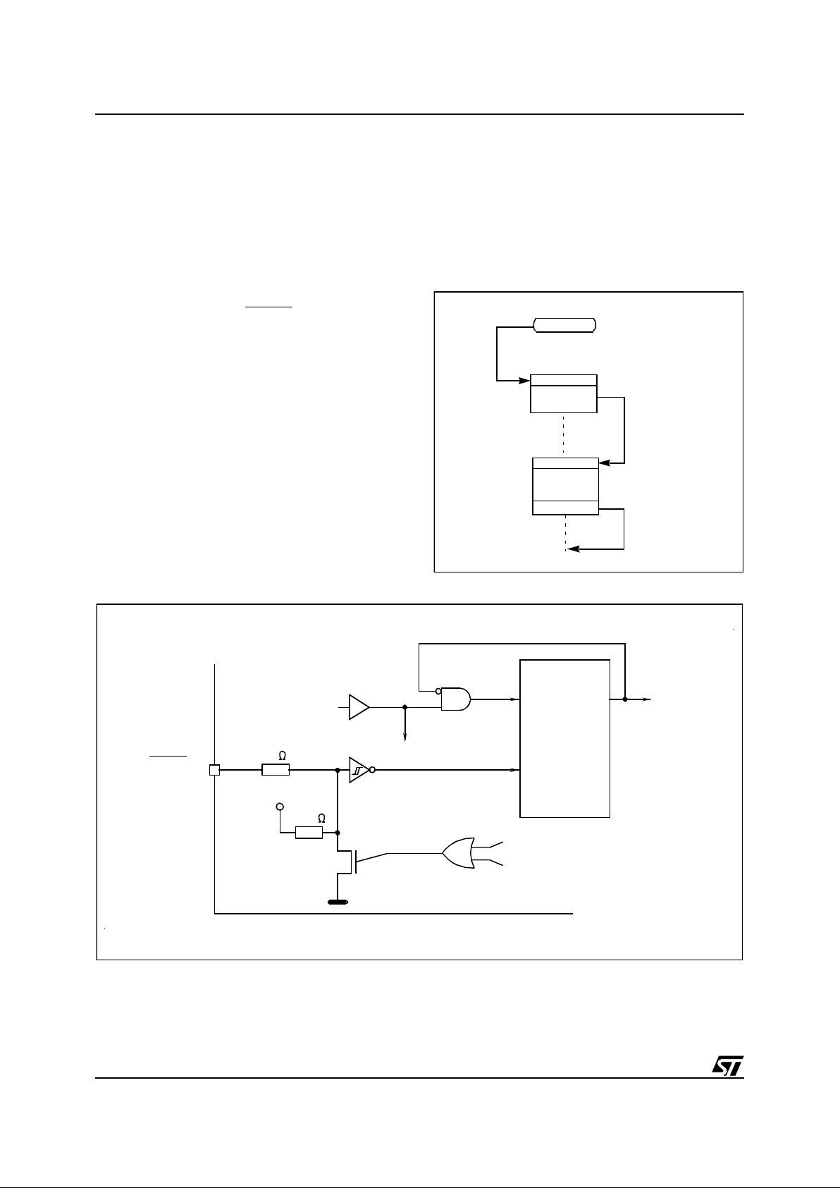
3.3 HARDWARE ACTIVATED DIGITAL WATCHDOG FUNCTION
The hardware activated digital watchdog func tion
consists of a down counter that is automatically initialized after reset so that this function does not
need to be activated by the user program. As the
watchdog function is always activated this down
counter can not be used as a timer. The watchdog
is using one data space register (HWDR location
D8h). The watchdog register is set to FEh on reset
and immediately starts to count down, requiring no
software start. Similarly the hardware activated
watchdog can not be stop ped or delayed by so ftware.
The watchdog time can be programmed us i ng the
6 MSBs in the watchdog register, this gives the
possibility to generate a reset in a time between
3072 to 196608 oscillator cycles in 64 possible
steps. (With a clock frequency of 8MHz this means
from 384ms to 24.576ms). The reset is prevented
if the register is reloaded with the desired value
before bits 2-7 decrement from all zeros to all
ones.
The presence of the hardware watchdog deactivates the STOP instruction and a WAIT instruction
is automatically executed instead of a STOP. Bit 1
of the watchdog register (set to one a t reset) can
be used to generate a soft ware reset if cleared t o
zero). Figure 17 shows the watchdog block dia-
gram while Figure 18 shows its working principle.
Figure 17. Hardware Activated Watchdog Block Diagram
RSFF
8
DATA BUS
VA00010
-2
-12
OSCILLATOR
RESET
WRITE
RESET
DB0
R
S
Q
DB1.7 SETLOAD
7
8
-2
SET
CLOCK
22/84
ST6365, ST6375, ST6385 ST6367, ST6377, ST6387
HARDWARE ACTIVATED DIGITAL WATCHDOG FUNCTION (Cont’d)
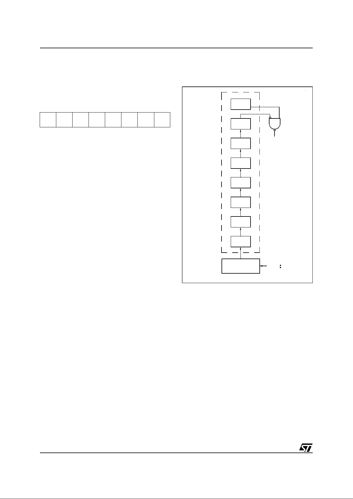
Hardware Activated Watchdog Register
(HWDR)
Address: D8h - Read/Write
Reset Value: 0FEh
T1-T6
. These are the watchdog counter bits. It
should be noted that D7 (T1) is the LSB of the
counter and D2 (T6) is the MSB of the counter,
these bits are in the opposite order to normal.
SR
. This bit is set to one during the reset phase
and will generate a software res et if clear ed to zero.
C
. This is the watchdog activation bit that is hardware set. The watchdog function is always activated independently of changes of value of this bit.
The register reset value is FEh (Bit 1-7 set to one,
Bit 0 cleared).
Figure 18. Har dw a re A ct iva te d Wa tc h dog
Working Princ iple
70
T1 T2 T3 T4 T5 T6 SR C
BIT0
VA00190
BIT1
BIT2
BIT3
BIT4
BIT5
BIT6
BIT7
8-BIT
DOWN COUNTER
OSC-12
WATCHDOG CONTROL REGISTER
RESET
D0
D1
D2
D3
D4
D5
D6
D7

23/84
ST6365, ST6375, ST6385 ST6367, ST6377, ST6387
3.4 INTERRUPT
The ST638x Core can m anag e 4 different maskable interrupt sources, pl us one non-maskable interrupt source (top priority level interrupt). Each
source is associated with a particular interrupt vector that contains a Jump instruction to the related
interrupt service routine. Each vector is located in
the Program Space at a particular address (see
Table 7). When a source provides an interrupt re-
quest, and the request processing is also enabled
by the ST638x Core, then the PC register is loaded with the address of the interrupt vector (i.e. of
the Jump instruction). Finally, the PC is loaded
with the address of the Jump instruction and the
interrupt routine is processed.
The relationship between vector and source and
the associated priority is hardware fixed for the different ST638x devices. For some interrupt sources it is also possible to select by software the kind
of event that will generate the interrupt.
All interrupts can be disabled by writing to the GEN
bit (global interrupt enable) of the interrupt op tion
register (address C8h). After a reset, ST638x is in
non maskable interrupt mode, so no interrupts will
be accepted and NMI flags will be used, until a
RETI instruction is executed. If an interrupt is executed, one special cycle is made by the core, during that the PC is set to the related interrupt vector
address. A jump instruction at this address has to
redirect program execution to the beginning of the
related interrupt routine. The interrupt detecting
cycle, also resets the related interrupt flag (not
available to the user), so that another interrupt c an
be stored for this current vector, while its driver is
under execution.
If additional interrupts arrive from the same
source, they will be lost. NMI can interrupt other interrupt routines at any time, while other interrupts
cannot interrupt each other. If more than one interrupt is waiting for service, they are executed according to their priority. The lower the number, the
higher the priority. Priority is, therefore, fixed. Interrupts are check ed dur i ng the last cycle of an instruction (RETI included). Level sensitive interrupts have to be valid during this period.
3.4.1 Interrupt Vectors/Sources
The ST638x Core includes 5 different interrupt
vectors in order to branch to 5 different interrupt
routines. The interrupt v ectors are located in the
fixed (or static) page of the Program Space.
The interrupt vector associated with the nonmaskab le interru p t so ur ce is named inter r up t v ec tor #0. It is located at the (FFCh,FFDh) addresses
in the Program Space. This vector is associated
with the PC6/IRIN pin.
The interrupt vectors located at addresses (F F6h,
FF7h), (FF4h, FF5h), (FF2h, FF3h), (FF0h, FF 1h)
are named interrupt vectors #1, #2, #3 and #4 respectively. These vectors are associated with TIMER 2 (#1), VSYNC (#2), TIMER 1 (#3) and
PC4(PWRIN) (#4).
Table 7. Interrupt Vectors/Sources
Relationships
Note 1
. This pin is associated with the NMI Inter-
rupt Vector
3.4.2 Interrupt Priority
The non-maskable interrupt request has the highest priority and can interrupt any other interrupt
routines at any time, nevertheless the other interrupts cannot interrupt each other. If more than one
interrupt request is pending, they are processed
by the ST638x Core according to their priority level: vector #1 has the higher priority while vector #4
the lower. The priority of each interrupt source is
hardware fixed.
Interrupt Source
Associated
Vector
Vector
Address
PC6/IRIN Pin
1
Interrupt
Vector # 0 (NMI)
0FFCh-0FFDh
Timer 2
Interrupt
Vector # 1
0FF6h-0FF7h
Vsync
Interrupt
Vector #2
0FF4h-0FF5h
Timer 1
Interrupt
Vector #3
0FF2h-0FF3h
PC4/PWRIN
Interrupt
Vector #4
0FF0h-0FF1h

24/84
ST6365, ST6375, ST6385 ST6367, ST6377, ST6387
INTERRUPTS
(Cont’d)
3.4.3 Interrupt Option Register
Interrupt Option Register (IOR)
Address: (C8h) - Write only
Reset Value: X000XXXXb
The Interrupt Option Register (IOR register, location C8h) is used to enable/disable the individual interrupt sources and to select the operating mode of
the external interrupt inputs. This register can be addressed in the Data Space as RAM location at the
C8h address, nevertheless it is a write-only register
that can not be accessed with single-bit operations.
The operating modes of the external interrupt inputs
associated to interrupt vectors #1 and #2 are selected through bits 5 and 6 of the IOR register.
Caution
:
This register contains at least one write
only bit. Single bit instructions (SET, RES, INC
and DEC) should not be used.
D7
. Not used.
EL1
. This is the Edge/Level selection bit of interrupt #1. When set to one, the interrupt is generated on low level of the related signal; when cleared
to zero, the interrupt is generated on falling e dge.
The bit is cleared to zero after reset.
ES2
. This is the edge selection bit on interrupt #2.
This bit is used on the ST638x devices with onchip OSD generator for VSYNC detection. When
this bit is se to one, the interrupt #2 is positive
edge sensitive, when cleared to zero t he ne gative
edge sensitive interrupt is selected.
GEN
. This is the global enable bit. When set to
one all interrupts are globally enabled; when this
bit is cleared to zero all interrupts are disabled (excluding NMI).
D3 - D0.
These bits are not used.
3.4.4 Interrupt Procedure
The interrupt procedure is very similar to a call procedure; the user can consider the interrupt as an
asynchronous call procedure. A s this is an asynchronous event the us er d oes not know about the
context and the time at which it occurred. As a result
the user should save all the data space registers
which will be used inside the interrupt routines.
There are separate sets of processor flags for normal, interrupt and non-maskable interrupt modes
which are automatically switc hed an d s o t hese do
not need to be saved.
The following list summarizes the interrupt procedure (refer also to Figure 19*)
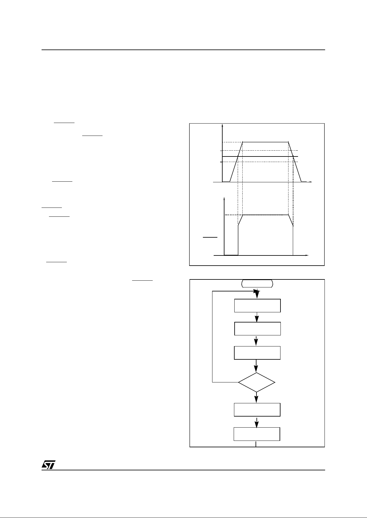
– Interrupt detection
– The flags C and Z of the main routine are ex-
changed with the flags C and Z of the interrupt
routine (resp. the NMI flags)
– The value of the PC is stored in the first level of
the stack - The normal interrupt lines are inhibit-
ed (NMI still active)
– The edge flip-flop is reset
– The related interrupt vector is loaded in the PC.
– User selected registers are saved inside the in-
terrupt service routine (normally on a software
stack)
– The source of the interrupt is found by polling (if
more than one source is associated to the same
vector)
– Interrupt servicing
– Return from interrupt (RETI)
– Automatically the ST638x core switches back to
the normal flags (resp the interrupt flags) and
pops the previous PC value from the stack
Figure 19. Interrupt Processing Flow-Cha rt
70
-
EL1 ES2 GEN
----
INSTRUCTION
FETCH
INSTRUCTION
EXECUTE
INSTRUCTION
WAS
THE INSTRUCTION
A RETI
?
?
CLEAR
INTERRUPT MASK
SELECT
PROGRAM FLAGS
“POP”
THE STACKED PC
?
CHECK IF THERE IS
AN INTERRUPT REQUEST
AND INTERRUPT MASK
SELECT
INTERNAL MODE FLAG
PUSH THE
PC INTO THE STACK
LOAD PC FROM
INTERRUPT VECTOR
(FFC/F FD )
SET
INTERRUPT MASK
NO
NO
YES
IS THE CORE
ALREADY IN
NORMAL MODE?
VA000014
YES
NO
YES

25/84
ST6365, ST6375, ST6385 ST6367, ST6377, ST6387
INTERRUPTS
(Cont’d)
The interrupt routine begins usually by the identification of the device that has generated the interrupt request. The user should save the registers
which are used inside the interrupt routine (that
holds relevant data) into a software stack. After the
RETI instruction execution, the Core carries out
the previous actions and the main routine can continue.
3.4.5 ST638x Interrupt Details
IR Interrupt (#0) .
The IRIN/PC6 Interrupt is connected to the first interrupt #0 (NMI, 0FFCh). If the
IRINT
interrupt is disabled at the Latch circuitry,
then it will be high. The #0 interrupt input detects a
high to low level. Note that once #0 has been
latched, then the only way to remove the latched
#0 signal is to service the interrupt. #0 can interrupt the other interrupts. A simple latch is provided
from the PC6(IRIN) pin in order to generate the IRINT signal. This latch can be triggered by e ither
the positive or negative edge of IRINT
signal. IRINT is inverted with respect to the latch. The latch
can be read by software and reset by software.
TIMER 2 Interrupt (#1).
The TIMER 2 Interrupt is
connected to the interrupt #1 (0FF6h). The TIMER
2 interrupt generates a low level (which is latched
in the timer). Only the low level selection for #1 can
be used. Bit 6 of the interrupt option register C8h
has to be set.
VSYNC Interrupt (#2).
The VSYNC Interrupt is
connected to the interrupt #2. When disabled the
VSYNC INT signal is low. The VSYNC INT signal
is inverted with respect to the signal applied to the
VSYNC pin. Bit 5 of the interrupt option register
C8h is used to select the negat ive edge (ES2= 0)
or the positive edge (ES2=1); the edge will depend
on the application. Note that once an edge has
been latched, then the only way to remove the
latched signal is to service the interrupt. Care must
be taken not to generat e spurious interrupt s. This
interrupt may be used to s ynchronize the VSYNC
signal in order to change characters in the OSD
only when the screen is on vertical blanking (if desired). This method may also be used to blink
characters.
TIMER 1 Interru pt (#3).
The TIMER 1 I nt errupt is
connected to the fourth interrupt #3 (0FF2h) which
detects a low level (latched in the timer).
PWR Interrupt (#4).
The PWR Interrupt is connected to the fifth interrupt #4 (0FF0h). If the
PWRINT is disabled at the PWR circuitry, then it
will be high. The #4 interrupt input detects a low
level. A simple latch is provided from the PC4
(PWRIN)pin in order to generate the PWRINT signal. This latch can be triggered by either the positive or negative edge of the PWRIN signal.
PWRINT is inverted with respect to the latch. The
latch can be reset by software.
Notes:
Global disable does not reset edg e sensitive interrupt flags. These edge sensitive interrupts
become pending again when global disabling is released. Moreover, edge sensitive interrupts are
stored in the related flags also when interrupts are
globally disabled, unless each edge sensitive interrupt is also individually disabled before the interrupting event happens. Global disabl e is done
by clearing the GEN bit of Interrupt option r egister,
while any individual disab le is done in the control
register of the peripheral. The on-chip Timer peripherals have an interrupt request flag bit (TMZ),
this bit is set to one when the device wants to generate an interrupt request and a mask bit (ETI) that
must be set to one to al low the trans fer of the flag
bit to the Core.

26/84
ST6365, ST6375, ST6385 ST6367, ST6377, ST6387
3.5 POWER SAVING MODES
STOP and WAIT m odes have be en implemented
in the ST638x in order to reduce the current consumption of the device d uring idle periods. These
two modes are described in the following paragraphs. Since the hardware activated digital
watchdog function is present, the STOP instruction is de-activated and any attempt to execute it
will cause th e automatic exe cution of a WAIT instruction.
3.5.1 WAIT Mode
The configuration of the MCU in the WAIT mode
occurs as soon as the WAIT instruction is executed. The microcontroller can also be considered as
being in a “software frozen” state where the Core
stops processing the instructions of the routine,
the contents of the RAM locations and peripheral
registers are saved as long as the power supply
voltage is higher than the RAM retention voltage
but where the peripherals are still working. The
WAIT mode is u sed when the us er wants to reduce the consumption of the MCU when it is in
idle, while not losing count of time or monitoring of
external events. The oscillator is not stopped in order to provide clock signal to the peripherals. The
timers counting may be enabled (writing the PSI
bit in TSCR1 regist er) and the timer i nte rrupt m ay
be also enabled bef ore entering th e WAIT m ode;
this allows the WAIT mode to be left when timer interrupt occurs. If the exit from the WAIT mode is
performed with a general RESET (either from the
activation of the external pin or by watchdog reset)
the MCU will enter a normal reset procedure as
described in the RESET chapter. If an interrupt is
generated during WAIT mode the M CU behavio ur
depends on the state of the MCU Core before the
initialization of the WAIT sequence, but also of the
kind of the interrupt request that is generated. This
case will be described in the following paragraphs.
In any case, the MCU Core does not generate any
delay after the occurrence of the interrupt because
the oscillator clock is still available.
3.5.2 STOP Mode
Since the hardware activated watchdog is present
on the ST638x, the STOP instruction has been deactivated. Any attempt to execute a STOP instruction will cause a WAIT i nstruction to be executed
instead.
3.5.3 Exit from WAIT Mode
The following paragraphs describe the output procedure of the MCU Core f rom WAIT mode when
an interrupt occurs. It must be noted that the restart sequence depends on the original state of the
MCU (normal, interrupt or non-maskable interrupt
mode) before the start of the WA IT s equence, but
also of the type of the interrupt request that is generated. In all cases the GEN bit of IOR has to be
set to 1 in order to restart from WAIT mode. Contrary to the operation of NM I in t he run m ode, the
NMI is masked in WAIT mode if GEN=0.
Normal Mode
. If the MCU Core was in the main
routine when the W AIT instruction has bee n executed, the Core exits from WAIT mode as soon as
an interrupt occurs; the corresponding interrupt
routine is executed, and at the end of the interrupt
service routine, the instruction that follows the
WAIT instruction is executed if no othe r interrupts
are pending.
Non-maskable Interrupt Mode
. If the WAIT instruction has been executed duri ng the execution
of the non-maskable interrupt routine, the MCU
Core outputs from WAIT mod e as soon as any interrupt occurs: the instruction that follows the
WAIT instruction is executed and the MCU Core is
still in the non-maskable interrupt mode even if another interrupt has been generated.
Normal Interrupt Mode
. If the MCU Core was in
the interrupt mode before the initialization of the
WAIT sequence, it outputs from the wait mode as
soon as any interrupt occurs. Nevertheless, two
cases have to be considered:
– If the interrupt is a normal interrupt, the interrupt
routine in which the WAIT was entered will be
completed with the execution of the instruction
that follows the WAIT and the MCU Core is still i n
the interrupt mode. At the end of this routine
pending interrupts will be serviced in accordance
to their priority.
– If t he interrupt is a non-maskable i nterrupt, the
non-maskable routine is processed at first. Then,
the routine in which the WAIT was entered will be
completed with the execution of the instruction
that follows the WAIT and the MCU Core is still i n
the normal interrupt mode.
Notes
:
If all the interrupt sources are disabled, the restart
of the MCU can only be done by a Reset activation. The Wait instru ction is not executed if an enabled interrupt request is pending. In ST638x devices, the hardware activated digital watchdog
function is present. As the watchdog is always activated, the STOP in struction is de-activated and
any attempt to exe cute the STOP instruction will
cause an execution of a WAIT instruction.
 Loading...