

SGS Thomson Microelectronics ST63T156B1, ST63T142B1, ST63T140B1, ST63T126B1, ST63142B1 Datasheet
...
ST63140, ST63146
ST63126, ST63156
DATA SHEET
1stEdition
OCTOBER 1993

USE INLIFE SUPPORTDEVICES OR SYSTEMS MUSTBE EXPRESSLYAUTHORIZED.
SGS-THOMSON PRODUCTS ARE NOT AUTHORIZED FOR USE AS CRITICAL COMPONENTS INLIFE SUPPORT DEVICES OR SYSTEMS WITHOUT THE EXPRESSWRITTEN APPROVAL OF SGS-THOMSON Microelectronics.
As used herein :
1. Life support devices or systems are those which (a) are
intended for surgical implant into the body, or (b) support
or sustain life, and whose failure to perform, when properly used in accordance with instructions for use provided with the product, can be reasonably expected to
result in significant injury to the user.
2. A criticalcomponent is any component of alife support
device or system whose failure to perform can reasonably be expected to cause the failure of the life support
device or system, or to affect its safety or effectiveness.

ST631xx DATASHEET INDEX
Pages
ST63140, ST63142
ST63126, ST63156
.................................... 1
GENERAL DESCRIPTION . . . . . . . . . . . . . . . . . . . . . . . . . . . . . . . . . . . . . . 3
PINDESCRIPTION ......................................... 5
ST631xxCORE . . . . . . . . . . . . . . . . . . . . . . . . . . . . . . ............. 7
MEMORYSPACES . . . . . . . . . . . . . . . . . . . . . . . . . . . . . . . . . . . ...... 10
STACKSPACE . . . . . . . . . . . . . . . . . . . . . . . . . . . . . . . . . . . . . . . . . . . 16
INTERRUPT . . . .......................................... 16
RESET . . . . . . . . . . . . . . . . . . . . . . . . . . . . . . . . . . . . . . . . . . . . . . . . 20
WAIT& STOPMODES . . . . . . . . . . . . . . . . . . . . . . . . . . . . . . . . . . . . . . . 22
ON-CHIPCLOCK OSCILLATOR . . . . . . . . . . . . . . . . . . . . . . . . . . . . . . . . . . 23
INPUT/OUTPUTPORTS . . . . . . . . . . . . . . . . . . . . . . . . . . . . . . . . . . . . . . 24
TIMERS . . . . . . . . . . . . . . . . . . . . . . . . . . . . . . . . . . . . . . . . . . . . . . . 27
HARDWARE ACTIVATEDDIGITALWATCHDOG FUNCTION . . . . . . ............. 30
SERIALPERIPHERALINTERFACE . . . . . . . . . . . . . . . . . . . . . . . . . . . . . . . . . 31
14-BITVOLTAGESYNTHESISTUNING
PERIPHERAL . . . . . . . . . . . . . . . . . . . . . . . . . . . . . . . . . . . . . . . . . . . . 40
6-BITPWMD/A CONVERTERAND 62.5kHz OUTPUT FUNCTION . . . . . . . . . . . . . . . . 41
AFC A/DINPUT,KEYBOARDINPUTS
AND BANDSWITHOUTPUTS . . . . . . . . . . . . . . . . . . . . . . . . . . . . . . . . . . . . 43
INFRAREDINPUT (IRIN) . . .................................... 44
ON-SCREENDISPLAY(OSD) . . . . . ............................... 45
SOFTWARE DESCRIPTION . . . . . ................................ 54
ABSOLUTEMAXIMUMRATINGS . . . . . . . . . . . . . . . . . . . . . ............. 59
EEPROMINFORMATION . . . . . . . . . . . . . . . . . . . . . . . . . . . . . . . . . . . . . . 60
PACKAGEMECHANICAL DATA . . . . . . . . . . . . . . . . . . . . . . . . . . . . . . . . . . 63
ORDERINGINFORMATIONTABLE . . . . . . . . . . . . . . . . . . . . . . . . . . . . . . . . . 65
ST63E140/T140, E142/T142
ST63E126/T126, E156/T156
............................. 67
GENERAL DESCRIPTION . . . . . . . . . . . . .......................... 69
PINDESCRIPTION ......................................... 71
EPROM/OTPDESCRIPTION. . . . . . . . . . . . . . . . . . ................... 74
ABSOLUTEMAXIMUMRATINGS . . . . . . . . . . . . . . . . . . . . . . . . . . . . . . . . . . 75
EEPROMINFORMATION . . . . . . . . . . . . . . . . . . . . . . . . . . . . . . . . . . . . . . 76
PACKAGEMECHANICAL DATA . . . . . . . . . . . . . . . . . . . . . . . . . . . . . . . . . . 79
ORDERINGINFORMATIONTABLE . . . . . . . . . . . . . . . . . . . . ............. 82

8-BIT HCMOS MCUs FOR
TV FREQUENCY & VOLTAGE SYNTHESIS WITHOSD
ST63140, ST63142
ST63126, ST63156
4.5 to6V operating Range
8MHzMaximum Clock Frequency
UserProgram ROM: 7948 bytes
Reserved Test ROM: 244 bytes
Data ROM: user selectablesize
Data RAM: 256 bytes
Data EEPROM: 128 bytes
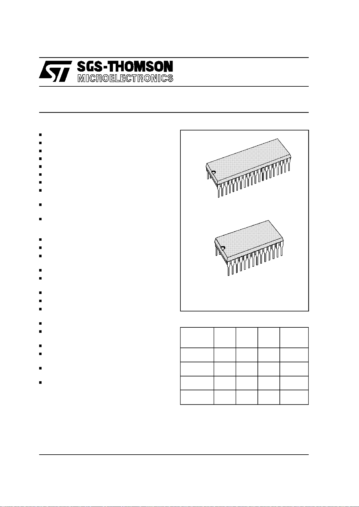
40-Pin Dual in Line Plastic Package for the
ST63126,156
28-Pin Dual in Line Plastic Package for the
ST63140,142
Up to 18 software programmable general pur-
pose Inputs/Outputs, including 8 direct LED
driving Outputs
3 Inputsfor keyboard scan (KBY0-2)
Up to 4 high voltage outputs(BSW0-3)
Two Timerseach includingan 8-bit counter with
a 7-bitprogrammable prescaler
Digital WatchdogFunction
Serial Peripheral Interface(SPI)supporting
S-BUS/I
2
C BUSand standardserial protocols
Up to Four 6-bit PWMD/A Converters
62.5kHz Output pin
14 bitcounter for voltagesynthesis tuning
(ST63156, ST63140)
AFCA/D converterwith 0.5V resolution
Four interrupt vectors (IRIN/NMI, Timer 1 & 2,
VSYNC.)
On-chipclock oscillator
5 Lines by 15 Characters On-ScreenDisplay
Generatorwith 128 Characters(2 banks)
All ROM types are supported by pin-to-pin
EPROMand OTP versions.
The development tool of the ST631xxmicrocon-
trollersconsistsof the ST63TVS-EMUemulation
and development system to be connectedvia a
standard RS232 serial line to an MS-DOSPersonal Computer.
This is Preliminary information from SGS-THOMSON. Details are subject tochange withoutnotice.
October 1993
PRELIMINARY DATA
DEVICE
ROM
(Bytes)
TUN. I/O Pins Package
ST63126 8K FS 12 PDIP40
ST63156 8K VS 11 PDIP40
ST63140 8K VS 6 PDIP28
ST63142 8K FS 6 PDIP28
DEVICE SUMMARY
1
PDIP28
1
PDIP40
(Ordering Information at the end of the datasheet)
1/82
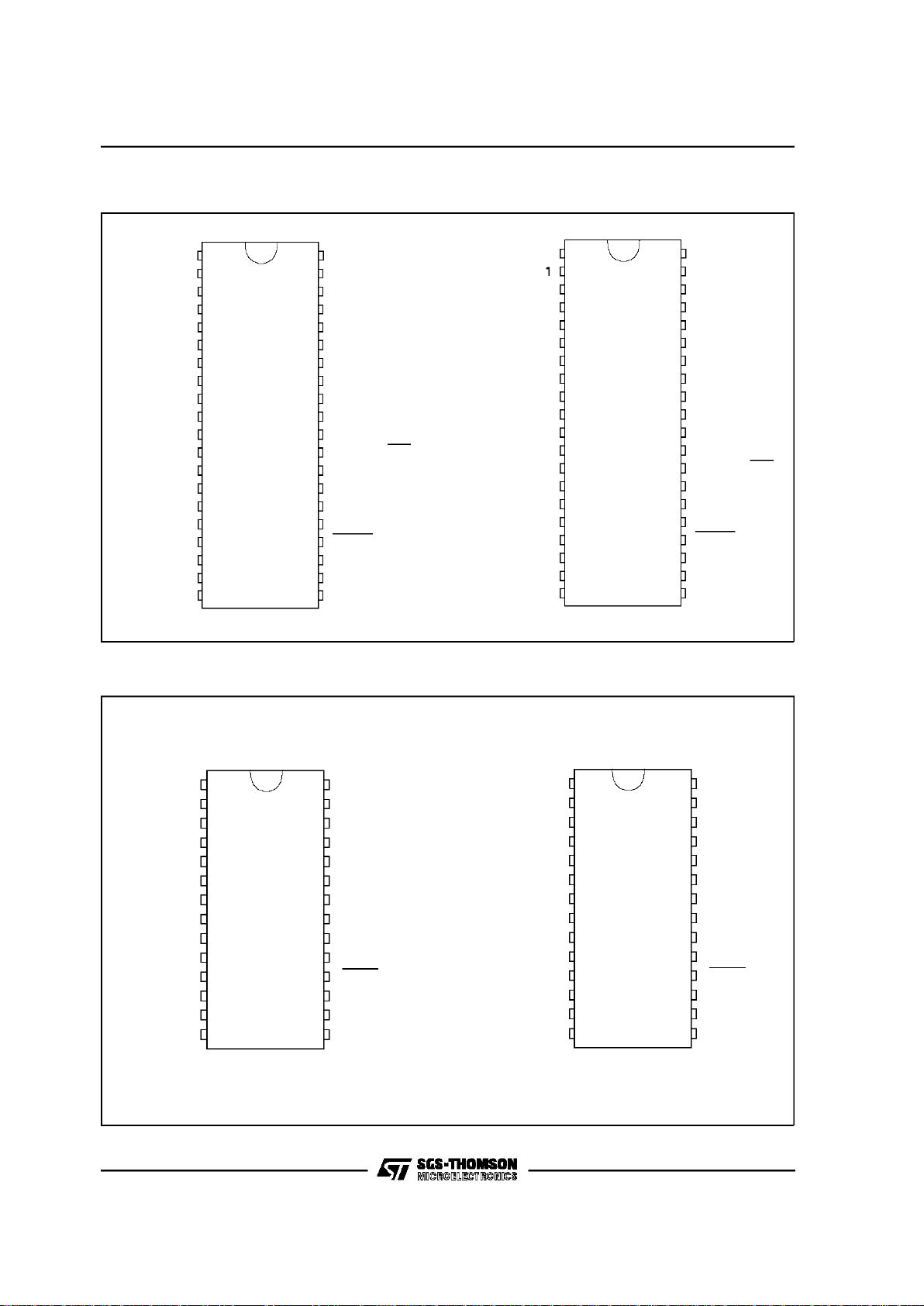
Figure1. ST63126, 156 Pin Configuration
Figure2. ST63140, 142 Pin Configuration
DA0
DA3
PC5 (R)
IRIN
OUT1
DA1
DA2
PA1
(SCL) PB5
(SDA) PB6
12
11
10
9
(SEN) PB7
KBY2
KBY
KBY0
8
7
6
5
BSW3
BSW2
BSW0
4
3
2
1
PA3
PA2
21
22
PA4
RESET
OSCin
OSCout
PC1
23
24
25
26
27
28
PA5
PA6
TEST
AFC
(VSYNC) PB2
(HSYNC) PB3
OSDOSCin
OSDOSCout
29
30
31
32
33
34
35
PC6 (G)
PC7 (B)
36
37
38
39
40
VA00282
V
DD
13
14
15
16
17
18
19
20
V
SS
1
BSW1
PC3 (BLANK)
PC2 (ON/OFF)
(1)
PC0
DA0
DA3
PC5 (R)
IRIN
OUT1
DA1
DA2
PA1
(SCL) PB5
(SDA) PB6
12
11
10
9
(SEN) PB7
KBY2
KBY
KBY0
8
7
6
5
BSW3
BSW2
BSW0
4
3
2
1
PA3
PA2
21
22
PA4
RESET
OSCin
OSCout
PC1
23
24
25
26
27
28
PA5
PA6
TEST
AFC
(VSYNC) PB2
(HSYNC) PB3
OSDOSCin
OSDOSCout
29
30
31
32
33
34
35
PC6 (G)
PC7 (B)
36
37
38
39
40
VA00288
V
DD
13
14
15
16
17
18
19
20
V
SS
1
BSW
PC3 (BLANK)
PC2 (ON/OFF)
VS
(1)
BSW0
BSW1
BSW2
KBY0
KBY1
KBY2
OSDOSCout
OSDOSCin
PB3 (HSYNC)
PB2 (VSYNC)
AFC
TEST
PA4
V
DA0
OUT1
VS
PC6 (G)
PC4
PC3 (BLANK)
PC2
OSCout
OSCin
RESET
PA0
PA1
PA2
1
2
3
4
5
6
7
8
9
10
11
12
13
14 15
16
17
18
19
20
21
22
23
24
25
26
27
28
VR001389
DD
V
SS
(1)
BSW0
BSW1
BSW2
KBY0
KBY1
KBY2
OSDOSCout
OSDOSCin
PB3 (HSYNC)
PB2 (VSYNC)
AFC
TEST
PA4
V
V
DA0
OUT1
IRIN
PC6 (G)
PC5 (R)
PC4
PC2
OSCout
OSCin
RESET
PA0
PA1
PA2
1
2
3
4
5
6
7
8
9
10
11
12
13
14 15
16
17
18
19
20
21
22
23
24
25
26
27
28
VR001390
DD
SS
(1)
Note 1. This pin isalso theVPPinputfor EPROM based devices
ST63126
ST63156
ST63140
ST63142
Note 1. This pin isalso theVPPinputfor EPROM based devices
ST63140,142,126,156
2/82

GENERAL DESCRIPTION
The ST63140, 142, 126, 156 microcontrollers are
members of the 8-bit HCMOS ST631xx family, a
series of devices specially oriented to TV applications.DifferentROMsizeand peripheralconfigurations areavailableto give themaximumapplication
and cost flexibility. All ST631xx members are
based on a building block approach: a common
core issurrounded by acombinationof on-chipperipherals(macrocells)available from a standard library. These peripherals are designed with the
same Core technology providing full compatibility
and short design time. Many of these macrocells
are specially dedicated to TV applications. The
macrocells of the ST631xx family are: two Timer
peripherals each includingan 8-bit counter with a
7-bit software programmable prescaler (Timer), a
digital hardware activated watchdog function
(DHWD), a 14-bitvoltage synthesis tuningperipheral, a Serial Peripheral Interface (SPI), up to four
6-bit PWM D/A converters,an AFCA/D converter
with 0.5V resolution, an on-screen display (OSD)
with 15 characters per line and 128 characters (in
two bankseach of 64 characters).In addition the
following memory resources are available: program ROM (7K),data RAM(256 bytes),EEPROM
(128 bytes).
Refer to pin configuration figures and to ST631xx
device summary (Table 1) for the definition of
ST631xx family members and asummaryof differences among the different types.
ST63140,142,126,156
3/82
STACK LEVEL 1
STACK LEVEL 2
STACK LEVEL 3
STACK LEVEL 4
STACK LEVEL 5
STACK LEVEL 6
PC
D/AOutputs
TIMER 2
IR INTERRUPT
Input
TEST
TIMER 1
PORT C
PORT B
PORT A
VS output &
AFC Input
ON-SCREEN
DISPLAY
DIGITAL
WATCHDOG/TIMER
SERIAL PERIPHERAL
INTERFACE
V
DD
V
SS
OSCin
OSDOSCin OSDOSCout
OSCout
RESET
R, G, B, BLANK
HSYNC (PB3)
VSYNC (PB2)
VR01753E
PA0 - PA7
*
DA0 - DA3
IRIN/NMI
TEST
AFC & VS
*
PB2 - PB7
*
PC0 - PC7
*
POWER SUPPLY OSCILLATOR RESET
8-BIT CORE
USER PROGRAM
ROM
8 KBytes
DATA ROM
USER SELECTABLE
DATA EEPROM
128 Bytes
DATA RAM
256 Bytes
* Refer To Pin Configuration For Additional Information
Figure3. ST631xx Block Diagram
DEVICE
ROM
(Bytes)
RAM
(Bytes)
EEPROM
(Bytes)
I/O
KBY
I/O
BSW
OUT
AFC VS D/A PACK.
EMUL.
DEVICES
ST63126 8K 256 128 12 3 4 YES NO 4 PDIP40 ST63E126
ST63156 8K 256 128 11 3 4 YES YES 4 PDIP40 ST63E156
ST63140 8K 256 128 6 3 3 YES YES 1 PDIP28 ST6E140
ST63142 8K 256 128 6 3 3 YES NO 1 PDIP28 ST63E142
Table 1. Device Summary
ST63140,142,126,156
4/82

PIN DESCRIPTION
V
DD
andVSS. Power issupplied to the MCU using
these twopins. V
DD
ispower and VSSistheground
connection.
OSCin, OSCout. These pins are internally con-
nected to the on-chip oscillator circuit. A quartz
crystal or a ceramic resonator can be connected
between these two pins in order to allow the correct operation of the MCU with various stability/cost trade-offs. The OSCin pin is the input pin,
the OSCoutpin is the output pin.
RESET. The activelow RESET pin is used to start
the microcontrollertothe beginningof its program.
TEST. The TEST pin mustbe held at V
SS
for nor-
mal operation.
PA0-PA7. These 8 linesare organizedas oneI/O
port (A). Eachline may be configuredas either an
input or as an output under softwarecontrol of the
data direction register. Port A has an open-drain
(12V drive) output configuration with direct LED
driving capability (30mA,1V).
PB2-PB3,PB5-PB7.These lines are organizedas
one I/O port (B). Each line may be configured as
either aninput withorwithoutinternalpull-up resistor or as an output under software control of the
data direction register. PB2-PB3 have a push-pull
configuration in output mode while PB5-PB7 are
open-drain (5Vdrive).
PB2 and PB3 lines are connected to the VSYNC
and HSYNCcontrol signals ofthe OSD cell;to provide the right signals to the OSD these I/O lines
should beprogrammedin input mode andthe user
can read “on the fly” the state of VSYNC and
HSYNC signals. PB2 is also connected with the
VSYNCInterrupt.The activepolarityofVSYNC Interrupt signalis softwarecontrolled. The activepolarity of these synchronization input pins to the
OSD macrocell can be selected by the user as
ROMmaskoption. Ifthe deviceis specified tohave
negative logic inputs, then when thesesignals are
low the OSD oscillatorstops. If the device is specified to have positivelogic inputs,then when these
signals are highthe OSDoscillatorstops.
PB5, PB6 and PB7 lines, when in output modes,
are “ANDed” with the SPI control signals. PB5 is
connected with the SPI clock signal (SCL), PB6
with the SPI data signal (SDA) while PB7 is connected with SPI enable signal (SEN).
PC0-PC7. These 8 lines are organized as oneI/O
port (C). Each line may be configured as either an
input with or without internal pull-up resistoror as
an output under softwarecontrol of the data direction register.PC0-PC2, PC4have apush-pull configuration in output mode while PC3, PC5-PC7
(OSDsignals)are open-drain(5V drive).PC3,PC5 ,
PC6 and PC7 lines when in output mode are
“ANDed” with the character and blank signals of
the OSD cell. PC3 is connected with the OSD
BLANKsignal,PC5,PC6 and PC7 withthe OSDR,
G and B signals. The active polarity of these signals canbe selected bythe userasROM maskoption. PC2 is also used as TV set ON-OFF switch
(5V drive).
DA0-DA3. These pins are the four PWM D/A outputs (with32kHzrepetition)ofthe6-bit on-chipD/A
converters.The PWM function can be disabledby
software and these lines can be used as general
purpose open-drain outputs (12V drive).
IRIN. This pin is the externalNMI of the MCU.
OUT1. This pin is the 62.5kHz output specially
suited to drivemulti-standard chroma processors.
This functioncan be disabled by software and the
pin can be used as general purpose open-drain
output (12V drive).
BSW0-BSW3. These output pins can be used to
selectupto 4tuningbands.These lines are configured asopen-drainoutputs (12Vdrive).
KBY0-KBY2.Thesepinsareinputonlyand can be
used forkeyboardscan. They have CMOS threshold levels with Schmitt Trigger and on-chip 100kΩ
pull-up resistors.
AFC. This is the input of theon-chip 10 level comparator that can be used to implement the AFC
function. This pin is an high impedance input able
to withstand signals with a peak amplitude up to
12V.
OSDOSCin, OSDOSCout. These are the On
Screen Display oscillator terminals. An oscillation
capacitorand coil network have tobeconnected to
provide theright signal to theOSD.
VS. This is the output pinof theon-chip 14-bitvoltage synthesis tuning cell (VS). The tuning signal
present at this pin gives anapproximate resolution
of 40kHz per stepover the UHFband.This lineis a
push-pull output with standard drive (ST63140,
ST63156 only).
ST63140,142,126,156
5/82

Pin Function Description
DA0 to DA3 Output, Open-Drain, 12V
BSW0 to BSW3 Output, Open-Drain, 12V
IRIN Input, Resistive Bias, Schmitt Trigger
AFC Input, High Impedance, 12V
OUT1 Output, Open-Drain, 12V
KBY0 to KBY2 Input, Pull-up, Schmitt Trigger
R,G,B, BLANK Output, Open-Drain, 5V
HSYNC, VSYNC Input, Pull-up, Schmitt Trigger
OSDOSCin Input, High Impedance
OSDOSCout Output, Push-Pull
TEST Input, Pull-Down
OSCin Input, Resistive Bias, Schmitt Trigger to Reset Logic Only
OSCout Output, Push-Pull
RESET Input, Pull-up, Schmitt Trigger Input
VS Output,Push-Pull
PA0-PA6 I/O, Open-Drain, 12V,No Input Pull-up, Schmitt Trigger, High Drive
PB2-PB3, PB5-PB7 I/O, Push-Pull, 5V, Input Pull-up, Schmitt Trigger
PB5-PB7 I/O, Open-Drain, 5V, Input Pull-up, Schmitt Trigger
PC0-PC2, PC4 I/O, Push-Pull, 5V, Input Pull-up, Schmitt Trigger
PC3, PC5-PC7 I/O, Open-Drain, 5V, Input Pull-up, Schmitt Trigger
V
DD,VSS
Power Supply Pins
Table 2. Pin Summary
ST63140,142,126,156
6/82
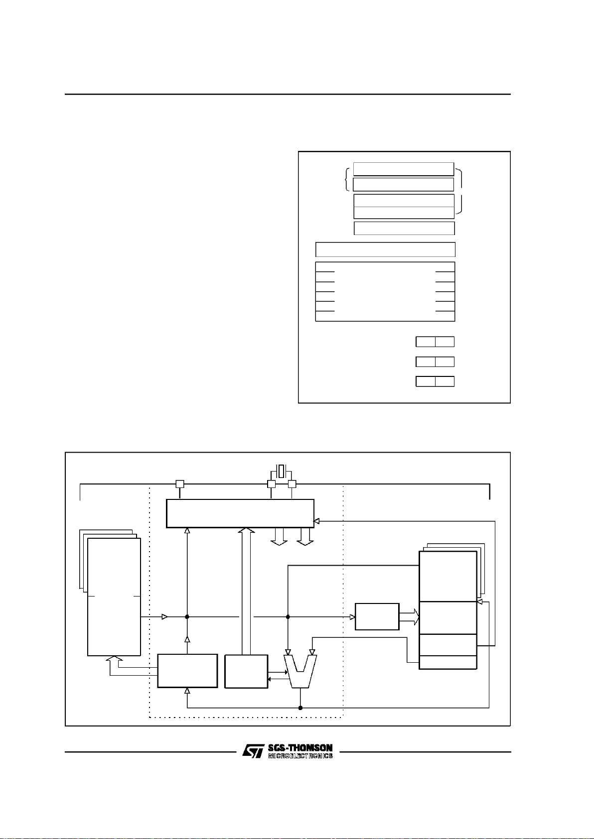
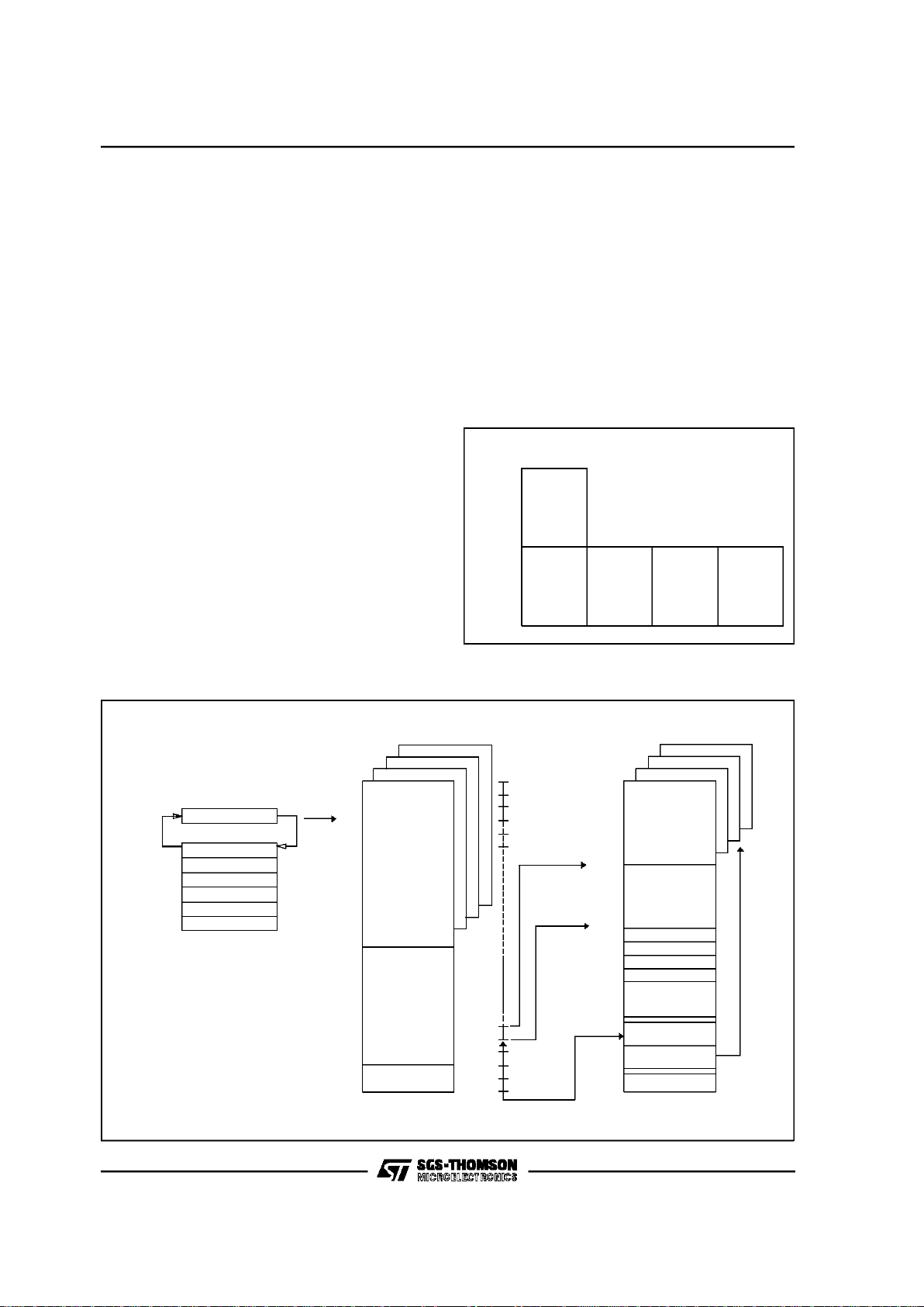
The Core of the ST631xx Family is implemented
independently from the I/O or memory configuration. Consequently,it can be treated as an independent centralprocessorcommunicatingwith I/O
and memoryvia internaladdresses,data,and control busses. The in-core communication is arranged as shown in the following block diagram
figure; thecontrollerbeing externallylinkedto both
the resetand theoscillator, whilethe core is linked
to thededicatedon-chip macrocellsperipheralsvia
the serial data bus and indirectly for interrupt purposes throughthe control registers.
Registers
The ST631xx Family Core has six registers and
three pairs of flags available to the programmer.
They are shown in Figure 5 and are explained in
the following paragraphs together with the program and data memorypage registers.
Accumulator (A). The accumulator is an 8-bit
general purpose register used in all arithmeticcalculations, logical operations, and data manipulations. The accumulator is addressed in the data
space asRAM locationat address FFh.
Accordingly, the ST631xx instruction set can use
the accumulatoras anyother register of the data
space.
VR001811
PROGRAM
ROM/EPROM
RESET
OPCODE
FLAG
VALUES
CONTROL
SIGNALS
12
FLAGS
ALU
A-DATA
B-DATA
2
256
DATA SPACE
DATA
RAM / EEPROM
DATA
ACCUMULATOR
INTERRUPTS
RESULTS TO DATA SPACE ( WRITE LINE )
0,01 TO 8MHz
ADDRESS / READ LINE
DEDICATIONS
CONTROLLER
ROM / EPROM
OSCin OSCout
ADDRESS
DECODER
Program Counter
and
6 LAYER STACK
Figure4. ST631xx Core Block Diagram
SHORT
DIRECT
ADDRESSING
MODE
V REGISTER
W REGISTER
PROGRAMCOUNTER
SIX LEVELS
STACKREGISTER
C
C
C
Z
Z
Z
NORMAL FLAGS
INTERRUPTFLAGS
NMI FLAGS
INDEX
REGISTER
VA000423
b7
b7
b7
b7
b7
b0
b0
b0
b0
b0
b0b11
ACCUMULATOR
Y REG. POINTER
X REG. POINTER
Figure5. ST631xx Core Programming Model
ST631xx CORE
ST63140,142,126,156
7/82

ST631xx CORE(Continued)
Indirect Registers (X, Y). These two indirect reg-
istersare usedas pointers tothe memorylocations
in the dataspace. They are usedin theregister-indirect addressing mode.These registers can be
addressed in the data space as RAM locations at
the 80h (X)and 81h (Y)addresses.They can also
be accessed with the direct, short direct, or bit direct addressing modes. Accordingly,the ST631xx
instructionsetcan use the indirect registers as any
other registerof the data space.
Short Direct Registers (V, W). These two registers are used to save one byte in short direct addressing mode.These registerscan be addressed
in the data space as RAM locations atthe 82h (V)
and 83H (W) addresses. They can also be accessed with the direct and bit direct addressing
modes. Accordingly, the ST631xx instruction set
can use the shortdirect registers as any other register ofthe data space.
Program Counter (PC)
The program counter is a 12-bit registerthat contains the address of the next ROM location to be
processed by the core. This ROM location may be
an opcode, an operand, or an address of operand.
The 12-bit length allows the direct addressing of
4096 bytes in the program space. Nevertheless, if
the program space contains more than 4096 locations, thefurtherprogram spacecan be addressed
by using theProgramROMPage Register.The PC
value isincremented,after it is read forthe address
of thecurrent instruction,by sendingit through the
ALU, so giving the addressof the next byte in the
program.Toexecuterelativejumpsthe PCand the
offset values are shifted through the ALU, where
they will be added, and the result is shifted back
into the PC. The program countercan be changed
in thefollowingways:
JP (Jump)instruction....PC= Jump address
CALL instruction...........PC=Call address
Relative Branch
instructions...................PC= PC+offset
Interrupt........................PC=Interrupt vector
Reset............................PC=Reset vector
RET &RETI instructions............PC=Pop (stack)
Normal instruction........PC= PC+1
Flags (C, Z)
The ST631xx Core includes three pairs of flags
that correspond to 3 different modes: normal
mode, interrupt mode and Non-Maskable-Interrupt-Mode. Each pair consists of a CARRY flag
and aZEROflag. One pair (CN,ZN) is used during
normal operation, one pair is used during the interrupt mode (CI,ZI) and one is used during the notmaskable interrupt mode (CNMI,ZNMI).
TheST631xxCoreuses the pairofflags that corresponds to the actualmode: as soonas aninterrupt
(resp.a Non-Maskable-Interrupt)isgenerated, the
ST631xx Core uses the interrupt flags (resp. the
NMI flags) instead of the normal flags. When the
RETI instruction is executed, the normal flags
(resp. the interrupt flags) are restoredif the MCU
was in the normal mode (resp. in the interrupt
mode) before the interrupt. Should be observed
that each flagset can only be addressedin its own
routine (Not-maskable interrupt, normal interrupt
or mainroutine).Theinterrupt flags arenot cleared
during thecontext switching and so, theyremain in
the state they were at the exit of the last routine
switching.
The Carry flag is set when a carry or a borrow occurs during arithmetic operations, otherwise it is
cleared. The Carry flag is also set to the value of
the bit tested in a bit test instruction, and participates in the rotate left instruction.
TheZeroflagissetif theresultofthelastarithmetic
or logical operation wasequal to zero, otherwise it
is cleared.
The switching between these three sets is automaticallyperformedwhen anNMI,an interrupt and
a RETI instructions occur. As the NMI mode is
automatically selected after the reset ofthe MCU,
the ST631xxCore uses at firstthe NMI flags.
ST63140,142,126,156
8/82

ST631xxx CORE(Continued)
Stack
The ST631xx Core includes true LIFO hardware
stack that eliminates the need fora stack pointer.
The stackconsists ofsixseparate12-bit RAMlocations that do not belong to the data space RAM
area. When a subroutine call (or interruptrequest)
occurs,the contentsofeach levelis shiftedinto the
next levelwhile the contentofthe PC is shiftedinto
the first level (the value of the sixth level will be
lost). When subroutine or interrupt return occurs
(RET or RETI instructions), the first levelregisteris
shifted back into the PCand thevalue ofeachlevel
is shifted back into the previous level. These two
operating modes are describedin Figure 6. Since
the accumulator,as all otherdata space registers,
is not stored inthis stack the handling ofthisregisters shall be performed inside the subroutine. The
stack pointer will remain in its deepest position,if
more than 6 calls or interrupts are executed, so
that the last return address will be lost. It will also
remain in its highest position if the stack is empty
and a RET or RETI is executed. In this case the
next instructionwill be executed.
WHEN CALL
OR
INTERRUPT REQUEST
OCCURS
STACK LEVEL 1
STACK LEVEL 1
STACK LEVEL 1
STACK LEVEL 1
STACK LEVEL 1
STACK LEVEL 1
PROGRAM COUNTER
RET OR RETI
WHEN
OCCURS
VA000424
Figure6. Stack Operation
ST63140,142,126,156
9/82
PROGRAM SPACE
VR001568
INTERRUPT &
RESET VECTORS
ACCUMULATOR
WREGISTER
RAM
DATA ROM
WINDOW
RAM / EEPROM
BANKING AREA
DATA SPACE
DATA RAM
BANK SELECT
DATA ROM
WINDOW SELECT
VREGISTER
YREGISTER
XREGISTER
0-63
0000h
07FFh
0800h
0FF0h
0FFFh
000h
03Fh
040h
070h
080h
081h
082h
083h
084h
0FFh
0C0h
ROM
ROM
STACKLEVEL 1
STACKLEVEL 2
STACKLEVEL 3
STACKLEVEL 4
STACKLEVEL 5
STACKLEVEL 6
PROGRAM COUNTER
STACK SPACE
Figure7. ST631xx Memory AddressingDescription Diagram
MEMORY SPACES
The MCUs operate in three different memory
spaces: Program Space, Data Space, and Stack
Space. A descriptionof these spaces is shown in
the followingFigures.
Program Space
The program space is physically implemented in
the ROM and includes all the instructionsthat are
to be executed, as well as the data requiredforthe
immediate addressing mode instructions, the reserved test area and uservectors. It is addressed
thanks to the 12-bit Program Counter register (PC
register)andso, the ST631xxCore can directlyaddress upto 4K bytesof Program Space.Nevertheless, the ProgramSpace can be extended by the
addition of 2-KbyteROM banks as it is shown in
Figure 8 in which the 8K bytes memory is described.
These banks are addressed by pointing to the
000h-7FFhlocations of the Program Spacethanks
to the Program Counter, and by writing the appropriate code in the Program ROM Page Register
(PRPR) located at address CAh of the Data
Space. Because interrupts and common subroutines should beavailableall the time onlythe lower
2K bytes of the 4K program space are bank
switched while the upper 2K bytescan be seen as
Program
counter
space
0000h 1FFFh
0FFFh
Static Page
Page 1
0800h
07FFh
Page 0
Page 1
Static Page
Page 2 Page 3
0000h
Figure8. ST631xx 8K Bytes ProgramSpace
AddressingDescription
staticspace. Table 3givesthecodesthat allow the
selection of the correspondingbanks.
Note that,fromthe memory point of view,thePage
1 and the StaticPage represent the same physical
memory:it isonly adifferentway ofaddressingthe
same location. On the ST631xx a total of 8192
bytes of ROM have been implemented; 7948 are
availableas user ROM while 244 are reserved for
testing.
ST63140,142,126,156
10/82
D7-D2. These bits are not used.
PRPR1-PRPR0. These are the program ROM
banking bits and thevalue loaded selects the corresponding page to be addressedin the lower part
of 4K programaddressspaceasspecifiedinTable3.
This registeris undefinedon reset.
Note:
Only the lower part of address space has been
bankswitched because interrupt vectors and common subroutines should be availableall the time.
The reasonof this structureis due tothe fact thatit
is notpossible tojump froma dynamic page to another, unless jumping back to the static page,
changingcontents of PRPR,and, then,jumping to
a differentdynamic page.
PRPR1 PRPR0 PC11 Memory Page
X X 1 Static Page (Page1)
0 0 0 Page 0
0 1 0 Page 1 (Static Page)
1 0 0 Page 2
1 1 0 Page 3
Table 3. Program ROM Page Register Coding
Care is required when handlingthe PRPR as it is
write only. For this reason, it is not allowed to
change the PRPR contents while executing interrupts drivers, as the driver cannot save and than
restore its previous content. Anyway, this operation may be necessary if thesum ofcommon routines and interrupt driverswill take more than 2K
bytes; in this case could benecessaryto divide the
interrupt driver in a (minor) part in the static page
(start and end), and in the second (major) part in
one dynamic page. If it is impossible to avoid the
writing of this register in interrupts drivers, an image of this register must be saved in a RAMlocation, and eachtime theprogramwrites the PRPRit
writes also the image register.The image register
must be written first, so if an interruptoccurs between the two instructions the PRPR is not affected.
MEMORY SPACES(Continued)
PRPR
Program ROMPage Register
(CAh, Write Only)
D7 D6 D5 D4 D3 D2 D1 D0
PRPR0 = PROG.ROMSelect0
PRPR1 = PROG.ROMSelect1
UNUSED
UNUSED
UNUSED
UNUSED
UNUSED
UNUSED
Figure11. Program ROM Page Register
ROM Page Device Address Device Address
(1)
Description
PAGE 0
0000h-007Fh
0080h-07FFh
0000h-007Fh
0080h-07FFh
Reserved
User ROM
PAGE 1
“STATIC”
0800h-0F9Fh
0FA0h-0FEFh
0FF0h-0FF7h
0FF8h-0FFBh
0FFCh-0FFDh
0FFEh-0FFFh
0800h-0F9Fh
0FA0h-0FEFh
0FF0h-0FF7h
0FF8h-0FFBh
0FFCh-0FFDh
0FFEh-0FFFh
User ROM
Reserved
Interrupt Vectors
Reserved
NMI Vector
Reset Vector
PAGE 2
0000h-000Fh
0010h-07FFh
1000h-100Fh
1010h-17FFh
Reserved
User ROM
PAGE 3
0000h-000Fh
0010h-07FFh
1800h-180Fh
1810h-1FFFh
Reserved
User ROM
Table 4. ST631xx Program ROM Map
Note 1. EPROM addresses relate to the use of ST63E1xx EPROMEmulation device.
This register is undefined on reset. Neither
read nor single bit instructions may be used to
address thisregister.
ST63140,142,126,156
11/82
b7 b0
000h
DATA RAM/EEPROM/OSD
BANK AREA
03Fh
040h
DATA ROM
WINDOW AREA
07Fh
X REGISTER 080h
Y REGISTER 081h
V REGISTER 082h
W REGISTER 083h
084h
DATA RAM
0BFh
PORT A DATA REGISTER 0C0h
PORT B DATA REGISTER 0C1h
PORT C DATA REGISTER 0C2h
RESERVED 0C3h
PORT ADIRECTION REGISTER 0C4h
PORT BDIRECTION REGISTER 0C5h
PORT C DIRECTION REGISTER 0C6h
RESERVED 0C7h
INTERRUPT OPTION REGISTER 0C8h
DATA ROMWINDOW REGISTER 0C9h
PROGRAM ROM PAGEREGISTER 0CAh
RESERVED 0CBh
SPIDATA REGISTER 0CCh
0CDh
RESERVED
0D1h
TIMER 1 PRESCALER REGISTER 0D2h
TIMER 1COUNTER REGISTER 0D3h
TIMER 1 STATUS/CONTROL REG. 0D4h
0D5h
RESERVED
0D7h
WATCHDOG REGISTER 0D8h
Figure12. ST631xx Data Space
b7 b0
RESERVED 0D9h
TIMER 2 PRESCALER REGISTER 0DAh
TIMER 2 COUNTER REGISTER 0DBh
TIMER 2 STATUS CONTROL REG. 0DCh
0DDh
RESERVED
0DFh
DA0 DATA/CONTROL REGISTER 0E0h
DA1 DATA/CONTROL REGISTER 0E1h
DA2 DATA/CONTROL REGISTER 0E2h
DA3 DATA/CONTROL REGISTER 0E3h
AFC RESULTREGISTER 0E4h
KEYBOARDINPUT REGISTER 0E5h
RESERVED 0E6h
RESERVED 0E7h
DATA RAM BANK REGISTER 0E8h
BSWCONTROL REGISTER 0E9h
EEPROM CONTROL REGISTER 0EAh
SPI CONTROL REGISTER 1 0EBh
SPI CONTROL REGISTER 2 0ECh
VS DATA REGISTER 1 0EDh
VS DATA REGISTER 2 0EEh
OSD CHARAC. BANK SELECTREG. 0EFh
0F0h
RESERVED
0FEh
ACCUMULATOR 0FFh
OSDCONTROLREGISTERSLOCATED
IN PAGE6 OFBANKED DATA RAM
VERTICAL STARTADDRESS REG. 010h
HORIZONTALSTARTADDRESSREG. 011h
VERTICAL SPACEREGISTER 012h
HORIZONTAL SPACEREGISTER 013h
BACKGROUND COLOUR REGISTER 014h
GLOBAL ENABLEREGISTER 017h
Figure13. ST631xx Data Space(Continued)
MEMORY SPACES(Continued)
Data Space
The instruction set of the ST631xx Core operates
on a specificspace, named DataSpace that contains all the data necessary for the processingof
the program. The Data Space allows the address-
ing of RAM (256 bytes for the ST631xx family),
EEPROM (128 bytes), ST631xx Core/peripheral
registers, and read-only data such as constants
and thelook-up tables.
ST63140,142,126,156
12/82

DWR
Data ROMWindow Register
(C9h, Write Only)
D7 D6 D5 D4 D3 D2 D1 D0
DWR0 = Data ROMWindow 0
DWR1 = Data ROMWindow 1
DWR2 = Data ROMWindow 2
DWR3 = Data ROMWindow 3
DWR4 = Data ROMWindow 4
DWR5 = Data ROMWindow 5
DWR6 = Data ROMWindow 6
UNUSED
Figure14. Data ROM Window Register
Data ROMAddressing.All theread-only data are
physically implemented in the ROM in which the
Program Space is also implemented. The ROM
thereforecontains theprogram tobe executedand
also the constants and the look-up tables needed
for the program. The locations of Data Space in
which the different constants and look-up tables
are addressed by the ST631xx Core can be considered as being a 64-byte window throughwhich
it ispossible toaccessto the read-only data stored
in the ROM. This window is located from address
40H toaddress 7Fh in the Dataspace and allows
the direct reading of the bytes from the address
000h to address03Fh in the ROM. All the bytesof
the ROMcan be usedto storeeither instructionsor
read-onlydata. Indeed,the window can be moved
by step of 64 bytes along the ROM in writing the
appropriatecodein the Write-only Data ROMWindow register(DRWR, location C9h).The effective
address ofthebyteto beread as adata in theROM
is obtained by the concatenation of the 6 lesssignificant bits of the addressin the Data Space (as
less significant bits)and the contentof theDRWR
(as most significant bits). So when addressing location 40h of data space, and 0 isloaded in the
DRWR, the physicaladdressed location in ROMis
00h.
D7. This bit is not used.
DWR6-DWR0.ThesearetheDataRomW in dowbits
thatcorrespondtotheupperbitsofdataROMprogram
space.Thisregisterisundefinedafterreset.
This register is undefined on reset. Neither
read nor single bit instructions may be usedto
address thisregister.
Note. Care is required when handlingthe DRWR
as it is write only. For this reason, it is not allowed
to change the DRWRcontents while executinginterruptsdrivers,as the drivercannot saveand than
restore its previous content. If it is impossible to
avoid the writing of this register in interrupts drivers, an image of this register must be saved in a
RAM location, and each time the program writes
the DRWRitwritesalsothe image register.The image register must be writtenfirst,so if an interrupt
occurs between the two instructions the DRWR
register is not affected.
MEMORY SPACES(Continued)
DATA ROM
WINDOW REGISTER
CONTENTS
DATA SPACE ADDRESS
40h-7Fh
IN INSTRUCTION
PROGRAM SPACE ADDRESS
65432 0
543210
543210
READ
1
67891011
0
1
VR01573B
12
1
0
DATA SPACE ADDRESS
59h
0000
0
1
00
1
11
Example:
(DWR)
DWR=28h
11000000001
ROM
ADDRESS:A19h
11
13
01
7
0
0
Figure15. Data ROM Window Memory Addressing
ST63140,142,126,156
13/82

DRBR
Data RAM
Bank Register
(E8h, Write Only)
D7 D6 D5 D4 D3 D2 D1 D0
DRBR0 = Data RAM Bank0
DRBR1= Data RAM Bank 0
DRBR2= Data RAM Bank 0
DRBR3= Data RAM Bank 0
DRBR4= Data RAM Bank 0
DRBR5= Data RAM Bank 0
DRBR6= Data RAM Bank 0
UNUSED
Figure16. Data RAM Bank Register
MEMORY SPACES(Continued)
Data RAM/EEPROM/OSDRAM Addressing
In all members of the ST631xx family 64 bytes of
data RAM are directly addressable in the data
space from 80h toBFh addresses.The additional
192 bytesof RAM, the 128 bytesof EEPROM,and
the OSD RAM can be addressedusing the banks
of 64 bytes located between addresses 00h and
3Fh.Theselection of the bankisdone byprogramming theDataRAM BankRegister(DRBR)located
at the E8h address of the Data Space. In thisway
each bankofRAM,EEPROMorOSDRAMcan select 64 bytes at a time. No more than one bank
should beset at a time.
D7. This bit is not used.
DRBR6, DRBR5.Each of these bits, when set,will
selectone OSDRAM register page.
DRBR4,DRBR3,DRBR2.Each of these bits,when
set,will select one RAM page.
DRBR1,DRBR0. These bits select the EEPROM
pages.
This register is undefined after reset. Neither
read nor single bit instructions may be used to
address thisregister.
Table 5 summarizes how to set the Data RAM
Bank Register in order to select the various banks
or pages.
Note :
Care is required when handling the DRBR asit is
write only. For this reason, it is not allowed to
change the DRBR contentswhile executing interrupts drivers, as the driver cannot save and than
restore its previous content. If it is impossible to
avoid the writing of this register in interrupts drivers, an image of this register must be saved in a
RAM location, and each time the program writes
the DRBRit writes also the image register.
The image registermustbe written first,so if an interrupt occurs between the two instructions the
DRBR is not affected.
DRBR Value
Selection
Hex. Binary
01h 0000 0001 EEPROM Page 0
02h 0000 0010 EEPROM Page 1
04h 0000 0100 RAM Page 2
08h 000 1000 RAM Page 3
10h 0001 0000 RAM Page 4
20h 0010 0000 OSD Page 5
40h 0100 0000 OSD Page 6
Table 5. Data RAMBank Register Set-up
ST63140,142,126,156
14/82

EEPROMDescription
The dataspace of ST631xxfamily from 00hto 3Fh
is paged as described in Table 5. 128 bytes of
EEPROMlocated in 2 pagesof 64 bytes (pages0,
and 1, see Table 5).
Through the programming of the Data RAM Bank
Register (DRBR=E8h) the user can select the
bank or page leaving unaffected the way to address the static registers. The way to address the
“dynamic”page is tosetthe DRBRas described in
Table 5(e.g.to selectEEPROMpage 0,the DRBR
has to be loaded with content 01h, see Data
RAM/EEPROM/OSD RAM addressing for additional information). Bits 0 and 1 of the DRBR are
dedicated tothe EEPROM.
The EEPROM pages do not require dedicated instructionstobeaccessed in reading or writing.The
EEPROM is controlled by the EEPROM Control
Register (EECR=EAh).AnyEEPROMlocation can
be read just like any other data location, also in
terms ofaccesstime.
To write an EEPROM location takes an average
time of 5 ms (10ms max) and during this timethe
EEPROM is not accessible by the Core. A busy
flag canbe readby the Coretoknow the EEPROM
status before trying any access. In writing the
EEPROM can work in two modes: Byte Mode
(BMODE) and Parallel Mode (PMODE). The
BMODE is the normal way to use the EEPROM
and consists in accessing one byte at a time. The
PMODE consists inaccessing 8 bytesper time.
D7. Not used
SB.WRITEONLY. Ifthis bit isset theEEPROMis
disabled (any accesswill be meaningless)and the
power consumption of the EEPROMis reducedto
the leakage values.
D5, D4.Reserved,they must be setto zero.
PS.SET ONLY. Oncein Parallel Mode,assoon as
the usersoftwaresets the PSbitthe parallelwriting
of the 8 adjacentregisters will start.PSis internally
reset at the end of the programming procedure.
Note that less than 8 bytes can be written; after
parallel programming the remaining undefined
bytes will haveno particular content.
PE.WRITE ONLY. This bit must be setby theuser
program in order to performparallel programming
(more bytes per time). IfPE is set and the “parallel
start bit” (PS) is low, up to8 adjacentbytes can be
written at the maximum speed, the content being
stored in volatile registers.These 8 adjacent bytes
can be considered as row, whose A7, A6, A5, A4,
A3 arefixed while A2, A1 and A0 are thechanging
bytes. PE is automatically reset at the end of any
parallelprogramming procedure.PE can be reset
by the user software before starting the programming procedure,leaving unchanged theEEPROM
registers.
BS.READ ONLY. This bit will be automaticallyset
by the CORE when the user program modifies an
EEPROMregister. The user program hasto test it
before any read or write EEPROM operation; any
attemptto access the EEPROM while “busy bit” is
setwillbeabortedandthewriting procedureinprogress completed.
EN. WRITE ONLY.This bit MUSTbe set to one in
order to write any EEPROM register. If the user
program will attempt to write the EEPROM when
EN= “0” the involved registers will be unaffected
and the“busy bit”will notbe set.
AfterRESETthecontentofEECRregist erwi llbe 00h.
Notes :
When the EEPROM is busy (BS=“1”) the EECR
can notbe accessed inwrite mode, it is only possible to read BSstatus.This implies that as long as
the EEPROM is busy it is not possible to change
the status of the EEPROM control register. EECR
bits 4 and 5 are reserved for test purposes, and
must never be set to “1”.
MEMORY SPACES(Continued)
EECR
EEPROM Control Register
(EAh, Read/Write)
D7 D6 D5 D4 D3 D2 D1 D0
EN = EEPROMEnable Bit
BS = EEPROM Busy Bit
PE = Parallel Mode Enable Bit
PS = Parallel Start Bit
Reserved (Mustbe set Low)
Reserved (Mustbe set Low)
SB =Stand-by Enable Bit
Unused
Figure17. EEPROM Control Register
ST63140,142,126,156
15/82

Additional Notes on Parallel Mode. If the user
wants to perform a parallel programming the first
action should be the set toone thePEbit; from this
moment the first time the EEPROM will be addressed in writing, the ROW address will be
latched and it will be possible to change it only at
the end ofthe programmingprocedureor by resetting PE without programming the EEPROM.After
the ROWaddress latching the Core can “see” just
one EEPROMrow (the selected one) and any attempt to write or read other rows will produceerrors. Donot read the EEPROMwhile PEis set.
As soon asPE bitis set,the 8volatile ROW latches
are cleared. From this moment the user can load
data in the whole ROW or just in a subset.PS setting willmodify the EEPROMregisterscorresponding to the ROW latches accessed after PE. For
example, if the software sets PE and accesses
EEPROM in writing at addresses 18h,1Ah,1Bh
and then sets PS, these three registers will be
modified atthe same time; theremainingbytes will
have no particular content. Note that PE is internally reset at the end of the programming procedure. This implies that the user must set PE bit
between two parallel programming procedures.
Anywaytheuser can set andthen resetPEwithout
performing any EEPROM programming. PS is a
set only bit and is internally reset atthe end of the
programming procedure. Note that ifthe usertries
to set PS while PE is not set there will not be any
programming procedure and thePS bit will be unaffected.Consequently PS bitcan notbe set if EN
is low. PS can be affectedby the user set if, and
only if,EN and PE bits are also set to one.
STACK SPACE
The stackspace consistsof six 12bit registersthat
are used for stacking subroutine and interrupt return addresses plus the current program counter
register.
MEMORY SPACES(Continued)
INTERRUPT
The ST631xxCore can manage 4 different maskable interrupt sources, plus one non-maskable interrupt source (top priority level interrupt). Each
sourceisassociated with aparticularinterruptvector that contains a Jump instruction to the related
interrupt serviceroutine. Each vector is located in
the Program Space at a particular address (see
Table 6). When a source provides an interruptrequest, and therequest processingis alsoenabled
by the ST631xx Core, then the PC register is
loaded withthe address of the interrupt vector (i.e.
of the Jump instruction). Finally, the PC is loaded
with theaddress of the Jumpinstructionand the interruptroutine isprocessed.
The relationship between vector and source and
the associatedpriority ishardware fixed for the different ST631xx devices. For some interrupt
sourcesit is also possible to selectby softwarethe
kind ofevent that will generate the interrupt.
All interruptscan be disabled by writingto theGEN
bit (global interruptenable) of the interrupt option
register(addressC8h). Aftera reset,ST631xxis in
non maskable interruptmode, so no interruptswill
be accepted and NMI flags will be used, until a
RETI instruction is executed.If an interruptis executed, one special cycle is made by the core,during that the PC is set to the related interrupt vector
address. A jump instructionat thisaddress has to
redirect program execution to thebeginningof the
relatedinterruptroutine.Theinterruptdetectingcycle, also resets the relatedinterrupt flag(not available to the user), so that another interrupt can be
stored for this current vector, while its driver is under execution.
If additionalinterruptsarrivefromthe same source,
they will be lost. NMI can interrupt other interrupt
routines at any time,while other interrupts cannot
interrupt each other. If more than one interrupt is
waiting forservice, they are executed according to
their priority. The lower the number, the higher the
priority. Priority is, therefore, fixed. Interrupts are
checked during the last cycle of an instruction
(RETIincluded). Level sensitive interrupts have to
be validduring this period.
ST63140,142,126,156
16/82
InterruptVectors/Sources
The ST631xx Core includes 5 different interrupt
vectors in order to branch to 5 different interrupt
routines. The interrupt vectors are located in the
fixed (or static)page of the Program Space.
The interruptvectorassociatedwith thenon-maskable interrupt source is named interrupt vector#0.
It is located at addresses FFCh,FFDh in the Program Space. This vector is associated with the
PC6/IRINpin.
The interrupt vectors located at addresses
(FF6h,FF7h), (FF4h,FF5h), (FF2h,FF3h),
(FF0h,FF1h) are named interrupt vectors #1, #2,
#3 and #4respectively.These vectorsare associated with TIMER 2 (#4), VSYNC (#2), and TIMER
1 (#3). Interrupt vector (#1) is not used on
ST631xx.
InterruptPriority
The non-maskable interrupt request has the highest priority and can interrupt any other interrupt
routines at any time, nevertheless the other interrupts cannot interrupteach other. Ifmore than one
interrupt requestis pending,they areprocessedby
the ST631xx Core according to their prioritylevel:
vector#1 has the higherprioritywhile vector#4the
lower. Thepriority of each interrupt sourceis hardware fixed.
InterruptOption Register
The Interrupt Option Register (IOR register, location C8h) is used to enable/disable the individual
interrupt sources and to select the operating mode
of theexternal interrupt inputs.Thisregistercanbe
addressed in the Data Space as RAM location at
the C8h address,nevertheless it is write-only register that can not be accessed with single-bit operations. The operating modes of the external
interrupt inputs associated to interrupt vectors #1
and #2are selectedthrough bits5 and6 of theIOR
register.
Interrupt
Source
Associated
Vector
Vector Address
IRIN/NMI
Pin
(1)
Interrupt
Vector # 0 (NMI)
0FFCh-0FFDh
None
(2)
Interrupt
Vector # 1
0FF6h-0FF7h
Vsync
Interrupt
Vector # 2
0FF4h-0FF5h
Timer 1
Interrupt
Vector # 3
0FF2h-0FF3h
Timer 2
Interrupt
Vector # 4
0FF0h-0FF1h
Notes:
1. This pin is associated with the NMIInterrupt Vector
2. This vectoris not used in ST631xx.
Table 6. Interrup tVectors/SourcesRelati ons hi ps
INTERRUPT(Continued)
IOR
InterruptOption Register
(C8h, Write Only)
D7 D6 D5 D4 D3 D2 D1 D0
Unused
GEN = Global EnableBit
ES2 = Edge SelectionBit
EL1 = EdgeLevelSelection Bit
Unused
Figure18. InterruptOption Register
D7. Not used.
EL1. This is the Edge/Level selection bit of inter-
rupt#1.When set to one,the interruptisgenerated
on low level of the related signal; when cleared to
zero,the interruptisgenerated on falling edge.The
bit iscleared tozero after reset and as nointerrupt
source is associated to vector#1 on ST631xx, the
user must keepthis bit atzeroto avoid ghostinterruptsfrom this source.
ES2. This is the edge selection bit on interrupt#2.
This bit is used on the ST631xx devices with onchip OSDgenerator for VSYNC detection.
GEN.This isthe global enablebit. When setto one
all interrupts are globallyenabled; when thisbit is
cleared to zero all interruptsare disabled(EXcluding NMI).
D3 - D0. Thesebits are not used.
ST63140,142,126,156
17/82

Interrupt Procedure. The interrupt procedure is
very similar to a call procedure, indeed the user
can considerthe interrupt asan asynchronouscall
procedure. As this is an asynchronous event the
user doesnot know about the contextand the time
at which it occurred. As a result the user should
saveall the dataspace registerswhich willbe used
inside the interrupt routines. There are separate
sets of processor flags for normal, interrupt and
non-maskable interrupt modes whichare automatically switched and so these do not need to be
saved.
The following list summarizes the interrupt procedure:
ST631xxactions
-
Interrupt detection
-
The flags C and Z of the main routine are exchanged with the flags C and Z of the interrupt
routine (orthe NMI flags)
-
The valueof thePC is storedin the firstlevel of
the stack
-
The normal interrupt lines are inhibited (NMI
still active)
-
First internal latch is cleared
-
The relatedinterrupt vectoris loaded inthe PC.
User actions
-
User selected registers are saved insidethe interrupt service routine (normally on a software
stack)
-
The source of the interrupt is found by polling
(if more than one source is associated to the
same vector)the interrupt flag of the source.
-
Interrupt servicing
-
Return from interrupt (RETI)
ST631xxactions
-
Automatically the ST631xx core switches back
to the normal flags (or the interrupt flags) and
pops the previous PC value fromthe stack
The interruptroutine begins usually by the identification of the device that has generated the interrupt request (bypolling).The user should save the
registers which are used inside the interrupt routine (thatholds relevantdata)intoa softwarestack.
After the RETIinstruction execution, the corecarries out theprevious actions and the main routine
can continue.
ST631xx InterruptDetails
IR Interrupt (#0). The IRIN Interrupt is connected
to the firstinterrupt #0 (NMI,0FFCh). If enabled,
then an interruptwill begenerated ona rising edge
at the pin.
Interrupt(#1).OnST631xx no sourcesareassociated to vector (#1). To avoid any ghost interrupt
due to interrupt(#1) the user must keep the EL1
bit ofIOR registerto zero.
INTERRUPT(Continued)
LOAD PC FROM
INTERRUPT VECTOR
( FF C / FFD )
SET
INTERRUPT MASK
PUSH THE
PC INTO THE STACK
SELECT
INTERNAL MODE FLAG
CHECK IF THERE IS
AN INTERRUPT REQUEST
AND INTERRUPT MASK
INSTRUCTION
WAS
THE INSTRUCTION
ARETI
IS THE CORE
ALREADY IN
NORMAL MODE ?
FETCH
INSTRUCTION
EXECUTE
INSTRUCTION
CLEAR
INTERRUPT MASK
SELECT
PROGRAM FLAGS
” POP ”
THE STACKED PC
NO
NO
YES
YES
?
?
NO
YES
VA000014
Figure19. InterruptProcessingFlow-Chart
ST63140,142,126,156
18/82

INTERRUPT(Continued)
VSYNC Interrupt (#2). The VSYNC Interrupt is
connected to the interrupt #2. When disabled the
VSYNC INT signal is low.Bit 5of the interrupt option register C8h is used to select the negative
edge (ES2=0) or the positive edge (ES2=1); the
edge willdependontheapplication.Notethat once
an edge has been latched, then the only wayto remove the latched signal is to service the interrupt.
Care mustbe takennotto generatespurious interrupts. This interruptmay be used for synchronize
to theVSYNCsignal inorder tochange characters
in the OSD only when the screen is on vertical
blanking (if desired). This method may also be
used toblink characters.
TIMER 1 Interrupt(#3). The TIMER 1 Interruptis
connected to the fourth interrupt#3 (0FF2h) which
detectsa low level(latched in the timer).
TIMER 2 Interrupt(#4). The TIMER 2 Interruptis
connected to the fifth interrupt #4 (0FF0h) which
detectsa high to low level (latched inthe timer).
Notes: Global disable does notreset edge sensitive interruptflags. These edge sensitive interrupts
becomependingagainwhenglobaldisablingis released. Moreover, edge sensitive interrupts are
stored in therelated flags also when interrupts are
globallydisabled,unlesseachedge sensitiveinterrupt is also individually disabled before the interrupting event happens. Global disable is done by
clearing the GEN bit of Interrupt option register,
while any individual disable is done in the control
register of the peripheral. The on-chip Timer peripherals have an interrupt request flag bit (TMZ),
this bit is setto one when the device wantsto generate an interruptrequest and amaskbit (ETI) that
must be setto one to allowthe transfer of the flag
bit tothe Core.
ST63140,142,126,156
19/82

Figure20. Internal Reset Circuit
The ST631xx device can be reset in twoways: by
the external reset input (RESET ) tied low, by
power-on reset and by the digital Watchdog peripheral.
RESETInput
The externalactive low RESET pin is usedto reset
the ST631xx devices and provide an orderly software startup procedure. The activation of the RESET pin may occur in the RUN or WAIT mode.
Even shortpulses at theresetpin will be accepted
since the reset signal is latched internally and is
only cleared after2048 clocks at the oscillator pin.
The clocksfrom the oscillator pin to the reset circuitry are buffered by a Schmitt Trigger so that an
oscillator in start-up conditions will not give spurious clocks. The MCU is configured in the Reset
mode aslong asthe signaloftheRESET pin is low.
The processing of the program is stopped andthe
standardInput/Outputports(portA, portBand port
C) are in the input state (except PC2). As soon as
the level on the RESETpin becomes high, the initialization sequence isexecuted.
WatchdogReset
The ST631xx devices are provided with an onchip hardware activated digital watchdogfunction
in order to provide a graceful recovery from a software upset. If the watchdog register is not refreshed and the end-of-countis reached, then the
reset state will be latched into the MCU and an internal circuit pulls down the RESET pin. Thisalso
resets the watchdog which subsequentlyturns off
the pull-down and activates the pull-up device at
the RESETpin. This causes the positive transition
at theRESETpin.The MCU will then exitthe reset
state after 2048 clocks on the oscillatorpin.
ApplicationNotes
An external resistor between V
DD
and reset pin is
not required becausean internal pull-up device is
provided. The user may prefer to add an external
pull-up resistor.
An internal Power-on device does notguarantee
that the MCU will exit the reset state when V
DD
is
above 4.5V and therefore the RESET pin should
be externallycontrolled.
RESET
ST63140,142,126,156
20/82

MCU InitializationSequence
When a reset occurs the stack is resetto the program counter,the PCis loaded with the address of
the reset vector (located in the program ROM at
addressesFFEh& FFFh).A jump instructionto the
beginning of the program has to be written into
these locations. After a reset a NMI is automatically activated so that the core is in non-maskable
interrupt mode to prevent false orghost interrupts
during therestartphase. Therefore the restartroutine should be terminated by a RETIinstruction to
switch to normal mode and enableinterrupts.If no
pendinginterrupt is presentat the end of thereset
routine the ST631xx will continue with the instruction after the RETI; otherwisethe pendinginterrupt
will be serviced.
RESET
IS RESET
STILL PRESENT ?
YES
NO
VA000427
NMI MASK SET
INT LATCH CLEARED
( IF PRESENT )
SELECT
NMI MODE FLAGS
PUT FFEh
ON ADDRESS BUS
LOAD PC
FROM RESET LOCATIONS
FFE / FFF
FETCH INSTRUCTION
Figure21. Reset & Interrupt Processing
Flow-Chart
JP
RESET VECTOR
INITIALIZATION
ROUTINE
JP: 2 BYTES/4 CYCLES
RETI: 1BYTES/2 CYCLES
RETI
VA000181
RESET
Figure22. Restart InitializationProgram
Flow-Chart
RESET(Continued)
ST63140,142,126,156
21/82

The STOP and WAIT modes have been implemented in theST631xxCore in order toreduce the
consumption of the device when the latter has no
instruction to execute. These two modes are described in the followingparagraphs. On ST631xx
as the hardware activated digital watchdog function ispresent the STOPinstructionis de-activated
and any attempt to executeit will cause the automatic executionof a WAIT instruction.
WAIT Mode
The configuration of the MCU in the WAIT mode
occurs as soon as the WAIT instruction is executed. The microcontroller can also be considered
as being in a “software frozen” state where the
Core stops processing the instructionsof the routine, thecontents of theRAM locations andperipheral registers are saved as long as the power
supply voltage is higher than the RAM retention
voltage but where theperipheralsare still working.
The WAITmodeis usedwhenthe userwantstoreduce theconsumptionoftheMCU whenit isinidle,
while not losing count of time or monitoring of external events.The oscillatoris not stopped in order
to provide clock signal to theperipherals. The timers countingmay be enabled (writing the PSI bit in
TSCR register)and the timer interruptmay bealso
enabled before entering the WAIT mode; this allows theWAITmode to be leftwhen timerinterrupt
occurs. If the exit from the WAIT mode is performed with a general RESET (either fromthe activation ofthe external pin orby watchdogreset) the
MCU will enter a normal reset procedure as described in the RESET chapter. If an interrupt is
generatedduring WAIT mode theMCU behaviour
dependson thestate of the ST631xx Core before
the initializationof the WAITsequence, but also of
the kind ofthe interrupt request that is generated.
This case will be described in the followingparagraphs. In any case, the ST631xx Core does not
generate any delay afterthe occurrenceof the interruptbecausetheoscillatorclock is still available.
STOP Mode
On ST631xx the hardware watchdog is present
and the STOPinstruction has been de-activated.
Any attempt to execute a STOP will cause the
automatic execution of a WAITinstruction.
Exit from WAIT Mode
The following paragraphsdescribe the outputprocedure of the ST631xx Core from WAIT mode
when an interrupt occurs. Itmust be notedthat the
restart sequence depends on the original state of
the MCU (normal, interruptor non-maskable interrupt mode) before the startof the WAITsequence,
but also ofthe type of the interrupt request that is
generated. In all cases the GENbit ofIOR has to
be set to 1 in order to restart from WAIT Mode.
Contraryto the operationof NMI in the RUN Mode,
the NMIis masked in WAITMode if GEN=0.
Normal Mode. If the ST631xx Core was in the
main routine when the WAIT instruction has been
executed, the ST631xxCore outputs from the wait
mode as soon as any interrupt occurs; the related
interrupt routine is executed and at the end of the
interrupt service routine the instruction that follows
the WAIT instruction is executed if no other interruptsare pending.
Non-maskable Interrupt Mode. If the WAIT instruction has been executedduring the execution
ofthenon-maskableinterruptroutine,the ST631xx
Core outputs fromthe wait modeas soon as any
interrupt occurs: the instruction that follows the
WAIT instruction is executed and the ST631xx
Core is still in the non-maskable interrupt mode
even ifanotherinterrupt has been generated.
Normal InterruptMode. If the ST631xx Corewas
in the interruptmode beforethe initialization of the
WAITsequence, it outputsfrom the wait mode as
soon as any interrupt occurs. Nevertheless, two
caseshave to be considered:
-
If the interrupt is a normal interrupt, the interrupt routine in which the WAITwas enteredwill
be completedwith the execution of the instruction that follows the WAIT and the ST631xx
Core is still in the interruptmode. At the end of
this routine pending interrupts will be serviced
in accordanceto their priority.
-
If the interrupt is a non-maskable interrupt, the
non-maskable routine is processed at first.
Then, the routine in which the WAIT was entered will be completed with the execution of
the instruction that follows the WAIT and the
ST631xx Core is still in the normal interrupt
mode.
Notes :
If all theinterrupt sources are disabled,the restart
oftheMCUcanonlybe done bya Resetactivation.
The Wait instruction is not executed if an enabled
interrupt request is pending. In the ST631xx the
hardware activated digital watchdog function is
present. As the watchdog is always activated the
STOP instruction is de-activated and any attempt
to executethe STOP instruction will cause anexecution of a WAITinstruction.
WAIT & STOPMODES
ST63140,142,126,156
22/82
 Loading...